US6232646B1 - Shallow trench isolation filled with thermal oxide - Google Patents
Shallow trench isolation filled with thermal oxideDownload PDFInfo
- Publication number
- US6232646B1 US6232646B1US09/082,607US8260798AUS6232646B1US 6232646 B1US6232646 B1US 6232646B1US 8260798 AUS8260798 AUS 8260798AUS 6232646 B1US6232646 B1US 6232646B1
- Authority
- US
- United States
- Prior art keywords
- region
- oxide
- shaped
- pads
- isolation trench
- Prior art date
- Legal status (The legal status is an assumption and is not a legal conclusion. Google has not performed a legal analysis and makes no representation as to the accuracy of the status listed.)
- Expired - Lifetime
Links
Images


Classifications
- H—ELECTRICITY
- H01—ELECTRIC ELEMENTS
- H01L—SEMICONDUCTOR DEVICES NOT COVERED BY CLASS H10
- H01L21/00—Processes or apparatus adapted for the manufacture or treatment of semiconductor or solid state devices or of parts thereof
- H01L21/70—Manufacture or treatment of devices consisting of a plurality of solid state components formed in or on a common substrate or of parts thereof; Manufacture of integrated circuit devices or of parts thereof
- H01L21/71—Manufacture of specific parts of devices defined in group H01L21/70
- H01L21/76—Making of isolation regions between components
- H01L21/762—Dielectric regions, e.g. EPIC dielectric isolation, LOCOS; Trench refilling techniques, SOI technology, use of channel stoppers
- H01L21/76202—Dielectric regions, e.g. EPIC dielectric isolation, LOCOS; Trench refilling techniques, SOI technology, use of channel stoppers using a local oxidation of silicon, e.g. LOCOS, SWAMI, SILO
- H01L21/76205—Dielectric regions, e.g. EPIC dielectric isolation, LOCOS; Trench refilling techniques, SOI technology, use of channel stoppers using a local oxidation of silicon, e.g. LOCOS, SWAMI, SILO in a region being recessed from the surface, e.g. in a recess, groove, tub or trench region
- H01L21/7621—Dielectric regions, e.g. EPIC dielectric isolation, LOCOS; Trench refilling techniques, SOI technology, use of channel stoppers using a local oxidation of silicon, e.g. LOCOS, SWAMI, SILO in a region being recessed from the surface, e.g. in a recess, groove, tub or trench region the recessed region having a shape other than rectangular, e.g. rounded or oblique shape
- H—ELECTRICITY
- H01—ELECTRIC ELEMENTS
- H01L—SEMICONDUCTOR DEVICES NOT COVERED BY CLASS H10
- H01L21/00—Processes or apparatus adapted for the manufacture or treatment of semiconductor or solid state devices or of parts thereof
- H01L21/70—Manufacture or treatment of devices consisting of a plurality of solid state components formed in or on a common substrate or of parts thereof; Manufacture of integrated circuit devices or of parts thereof
- H01L21/71—Manufacture of specific parts of devices defined in group H01L21/70
- H01L21/76—Making of isolation regions between components
- H01L21/762—Dielectric regions, e.g. EPIC dielectric isolation, LOCOS; Trench refilling techniques, SOI technology, use of channel stoppers
- H01L21/76224—Dielectric regions, e.g. EPIC dielectric isolation, LOCOS; Trench refilling techniques, SOI technology, use of channel stoppers using trench refilling with dielectric materials
- H01L21/76232—Dielectric regions, e.g. EPIC dielectric isolation, LOCOS; Trench refilling techniques, SOI technology, use of channel stoppers using trench refilling with dielectric materials of trenches having a shape other than rectangular or V-shape, e.g. rounded corners, oblique or rounded trench walls
Definitions
- the present inventionrelates to integrated circuits and fabrication techniques for forming field oxide (FOX) regions on the integrated circuit substrate. More particularly, the present invention relates to fabrication techniques for forming shallow trench isolation (STI) regions on the integrated circuit substrate.
- FOXfield oxide
- STIshallow trench isolation
- the processes for fabricating semiconductor devicesincludes process steps for providing isolation regions that contain dielectric materials that provide the necessary protection for assuring proper function of the formed electronic integrated circuit design.
- the processincludes LOCOS which is localized oxidation of silicon. This process typically begins by depositing a silicon nitride layer over a silicon dioxide layer (barrier oxide) to a thickness in the range of 0.05 ⁇ m. to 0.10 ⁇ m. The silicon nitride is typically deposited using low-pressure chemical vapor deposition (LPCVD) techniques.
- LPCVDlow-pressure chemical vapor deposition
- a photoresist mask layercomprising any appropriate commercially available photoresist material known in the industry, is then deposited over the silicon nitride layer The photoresist mask layer is then patterned for forming isolation trenches.
- the isolation trench regionsare formed adjacent silicon oxide layer and the silicon nitride layer and a portion of the photoresist layer.
- the upper surface of the substrateis etched a small amount, approximately 0.25 ⁇ m.
- An oxide layeris formed in the isolation regions by depositing a thick pad of silicon dioxide using tetraethylorthosilicate (TEOS) as the source for deposition of silicon dioxide.
- TEOStetraethylorthosilicate
- the thickness of the oxide padalso referred to as a field oxide (FOX) pad, is in the range of 1.2 ⁇ m to 1.5 ⁇ m.
- the processfurther includes polishing of the formed isolation pads to a surface level and thickness substantially even with the silicon nitride level.
- the silicon nitride and silicon dioxide layer regionsare removed by wet etching to expose the active region which will be used to form the various integrated circuit components.
- the wet etchingis typically done using hot phosphoric acid to first etch the silicon nitride layer, then by dipping the substrate in a hydrofluoric acid (HF) dip to etch the silicon dioxide layer.
- HFhydrofluoric acid
- a primary object of the present inventionis to provide a method for forming isolation trenches such that the adjacent structure protecting the active semiconductor substrate is not eroded during etching processes used to form the trench regions.
- the foregoing objectis accomplished by providing a semiconductor substrate member fabricated having a thin barrier oxide layer on which are fabricated a plurality of spaced apart silicon nitride pads.
- the regions between the spaced apart nitride padsdelineate U-shaped regions for forming shallow isolation trenches and are layered with silicon oxide and polysilicon.
- the U-shaped regionsprovide a buffer region of oxide and polysilicon material adjacent opposing silicon nitride pads that prevent erosion of the nitride during etch formation of the isolation trench.
- the polysiliconis further etched to form a wider, second U-shaped region having sloped sidewalls that provide opposing spacerforming buffer material that facilitates forming a V-shaped isolation trench region into the semiconductor substrate member a predetermined depth without eroding the silicon nitride pads.
- the V-shaped trenchis subsequently filled with silicon dioxide that is grown by a hot thermal oxide process.
- the upper portion of the V-shaped isolation trenchmay be further filled with deposited silicon dioxide followed by a chemical mechanical polishing process.
- FIG. 1is a cross-sectional view of first U-shaped notch in a region delineated for forming shallow isolation trenches in accordance with the present invention.
- FIG. 2is a cross-sectional view of a second U-shaped notch having sloped sidewalls that form opposing spacer region comprising tapering amounts of oxide and polysilicon material that prevent erosion of the silicon nitride pads.
- FIG. 3is a cross-sectional view of a V-shaped isolation trench region fabricated into said semiconductor substrate member in accordance with the present invention.
- FIG. 4is a cross-sectional view of a V-shaped isolation trench region formed as shown in FIG. 3 and further showing a trench isolation material comprising silicon dioxide grown within a substantial portion of the V-shaped trench region.
- FIG. 5is a cross-sectional view of a V-shaped isolation trench region formed as shown in FIG. 4 further showing an upper end of the V-shaped isolation trench region with deposited silicon dioxide material in accordance with the present invention.
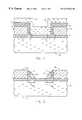
- FIGS. 1-5comprise trench isolation fabrication steps for use in fabrication of the shallow trench isolation structure in accordance with the present invention.
- a semiconductor substrate member 10has been fabricated to a stage such that a barrier oxide layer 11 , comprising a first silicon dioxide layer, has been formed overlaying silicon substrate 10 .
- FIG. 1also shows a plurality of spaced apart silicon nitride pads 14 that have been fabricated over portions of barrier oxide layer 11 .
- a second silicon oxide layer 12comprising, by example, a hot thermal oxide, is grown over, and on sidewall portions, of the silicon nitride pads 14 , as well as over portions of barrier oxide 11 in the regions between the silicon nitride pads 14 .
- the regions between silicon nitride pads 14comprising regions for forming shallow isolation trenches.
- a polysilicon layer 13is formed over the oxide layer 12 such that the polysilicon layer 13 forms a first U-shaped notch in the region delineated for forming said shallow isolation trenches.
- the material comprising the polysilicon 13 and hot thermal oxide 12provides a buffer region for shaping the isolation trench and protecting the corners of the nitride pads 14 during an etching process step.
- FIG. 2shows a first etching step that shapes the first U-shaped notch of polysilicon material such that a wider, second U-shaped notch is formed.
- the second U-shaped notchis formed such that spacers S are formed comprising buffer material region of oxide and polysilicon material that offset the nitride pads a varying distance Ws.
- spacers Sfacilitate forming a V-shaped isolation trench region T into semiconductor substrate member 10 .
- the width Ws of spacers Sare reduced by etching action while isolation trench region T is being fabricated.
- all of the polysilicon material 13comprising sidewalls of the second U-shaped notch, are etched away during formation of trench T, leaving a remaining oxide spacer S.
- the V-shaped isolation trench structurecomprises an upper end portion forming an opening having a width W t measuring, by example 0.2 ⁇ m, and a bottom end portion having a width W b measuring substantially less than 0.2 ⁇ m.
- the V-shaped trench Tis etched into semiconductor substrate 10 a predetermined depth dt ranging from 500 ⁇ to 2000 ⁇ .
- an isolation material 15is grown from the opposing silicon sidewall structure in the trench region.
- the isolation material 15is grown, by example using a hot thermal oxide HTO process.
- the oxide material 11 , 12 in the upper trench regiongets thicker during the HTO process.
- the extremely small dimensions associated with trench structure Tfacilitate a pinching effect of the oxide material being grown to fill the trench region.
- FIG. 4shows oxide material 15 filling a substantial portion of the V-shaped trench T. Also as seen in FIG. 4, the upper portion of the V-shaped trench adjacent the spacers S x are void of oxide material.
- FIG. 5shows additional oxide material 16 deposited over oxide material 15 to complete formation and filling of trench T. The additional oxide material is deposited by industry known chemical vapor deposition method. A roughness in the structure is polished by chemical mechanical polishing techniques.
Landscapes
- Engineering & Computer Science (AREA)
- Physics & Mathematics (AREA)
- Condensed Matter Physics & Semiconductors (AREA)
- General Physics & Mathematics (AREA)
- Manufacturing & Machinery (AREA)
- Computer Hardware Design (AREA)
- Microelectronics & Electronic Packaging (AREA)
- Power Engineering (AREA)
- Element Separation (AREA)
Abstract
Description
Claims (2)
Priority Applications (5)
| Application Number | Priority Date | Filing Date | Title |
|---|---|---|---|
| US09/082,607US6232646B1 (en) | 1998-05-20 | 1998-05-20 | Shallow trench isolation filled with thermal oxide |
| TW088107569ATW520548B (en) | 1998-05-20 | 1999-05-11 | Shallow trench isolation filled with thermal oxide |
| JP17881199AJP3703069B2 (en) | 1998-05-20 | 1999-05-20 | Method for forming shallow trench isolation |
| KR1019990018256AKR100675962B1 (en) | 1998-05-20 | 1999-05-20 | Thermal oxide-filled shallow device isolation trench |
| US09/784,892US6444539B1 (en) | 1998-05-20 | 2001-02-15 | Method for producing a shallow trench isolation filled with thermal oxide |
Applications Claiming Priority (1)
| Application Number | Priority Date | Filing Date | Title |
|---|---|---|---|
| US09/082,607US6232646B1 (en) | 1998-05-20 | 1998-05-20 | Shallow trench isolation filled with thermal oxide |
Publications (1)
| Publication Number | Publication Date |
|---|---|
| US6232646B1true US6232646B1 (en) | 2001-05-15 |
Family
ID=22172223
Family Applications (1)
| Application Number | Title | Priority Date | Filing Date |
|---|---|---|---|
| US09/082,607Expired - LifetimeUS6232646B1 (en) | 1998-05-20 | 1998-05-20 | Shallow trench isolation filled with thermal oxide |
Country Status (4)
| Country | Link |
|---|---|
| US (1) | US6232646B1 (en) |
| JP (1) | JP3703069B2 (en) |
| KR (1) | KR100675962B1 (en) |
| TW (1) | TW520548B (en) |
Cited By (10)
| Publication number | Priority date | Publication date | Assignee | Title |
|---|---|---|---|---|
| US6440817B2 (en)* | 2000-03-01 | 2002-08-27 | Micron Technology, Inc. | Methods of forming integrated circuitry |
| US6727150B2 (en) | 2002-07-26 | 2004-04-27 | Micron Technology, Inc. | Methods of forming trench isolation within a semiconductor substrate including, Tshaped trench with spacers |
| US20040080019A1 (en)* | 2001-07-13 | 2004-04-29 | Oh Yong-Chul | Methods for manufacturing integrated circuit devices including an isolation region defining an active region area |
| US20060108647A1 (en)* | 2004-11-23 | 2006-05-25 | Yuan Jack H | Self-aligned trench filling for narrow gap isolation regions |
| US20060110880A1 (en)* | 2004-11-23 | 2006-05-25 | Yuan Jack H | Self-aligned trench filling with high coupling ratio |
| US20060240660A1 (en)* | 2005-04-20 | 2006-10-26 | Jin-Sheng Yang | Semiconductor stucture and method of manufacturing the same |
| US20080157169A1 (en)* | 2006-12-28 | 2008-07-03 | Yuan Jack H | Shield plates for reduced field coupling in nonvolatile memory |
| US20080160680A1 (en)* | 2006-12-28 | 2008-07-03 | Yuan Jack H | Methods of fabricating shield plates for reduced field coupling in nonvolatile memory |
| CN102117762B (en)* | 2010-01-05 | 2012-11-07 | 上海华虹Nec电子有限公司 | Shallow trench isolation channel |
| CN110416089A (en)* | 2019-07-31 | 2019-11-05 | 上海华虹宏力半导体制造有限公司 | A kind of preparation method of LDMOS |
Families Citing this family (1)
| Publication number | Priority date | Publication date | Assignee | Title |
|---|---|---|---|---|
| KR100458767B1 (en)* | 2002-07-04 | 2004-12-03 | 주식회사 하이닉스반도체 | Method of forming a isolation layer in a semiconductor device |
Citations (8)
| Publication number | Priority date | Publication date | Assignee | Title |
|---|---|---|---|---|
| US5679599A (en)* | 1995-06-22 | 1997-10-21 | Advanced Micro Devices, Inc. | Isolation using self-aligned trench formation and conventional LOCOS |
| US5747866A (en)* | 1995-09-21 | 1998-05-05 | Siemens Aktiengesellschaft | Application of thin crystalline Si3 N4 liners in shallow trench isolation (STI) structures |
| US5798553A (en)* | 1995-01-10 | 1998-08-25 | International Business Machines Corporation | Trench isolated FET devices, and method for their manufacture |
| US5868870A (en)* | 1992-12-10 | 1999-02-09 | Micron Technology, Inc. | Isolation structure of a shallow semiconductor device trench |
| US5895253A (en)* | 1997-08-22 | 1999-04-20 | Micron Technology, Inc. | Trench isolation for CMOS devices |
| US5910018A (en)* | 1997-02-24 | 1999-06-08 | Winbond Electronics Corporation | Trench edge rounding method and structure for trench isolation |
| US5945724A (en)* | 1998-04-09 | 1999-08-31 | Micron Technology, Inc. | Trench isolation region for semiconductor device |
| US6064104A (en)* | 1996-01-31 | 2000-05-16 | Advanced Micro Devices, Inc. | Trench isolation structures with oxidized silicon regions and method for making the same |
Family Cites Families (3)
| Publication number | Priority date | Publication date | Assignee | Title |
|---|---|---|---|---|
| JPH07122627A (en)* | 1993-10-22 | 1995-05-12 | Sony Corp | Fabrication of semiconductor device |
| JPH08316224A (en)* | 1995-05-18 | 1996-11-29 | Sony Corp | Element isolation method and manufacture of semiconductor device |
| KR980012278A (en)* | 1996-07-12 | 1998-04-30 | 원본미기재 | Semiconductor device isolation process |
- 1998
- 1998-05-20USUS09/082,607patent/US6232646B1/ennot_activeExpired - Lifetime
- 1999
- 1999-05-11TWTW088107569Apatent/TW520548B/ennot_activeIP Right Cessation
- 1999-05-20JPJP17881199Apatent/JP3703069B2/ennot_activeExpired - Fee Related
- 1999-05-20KRKR1019990018256Apatent/KR100675962B1/ennot_activeExpired - Fee Related
Patent Citations (8)
| Publication number | Priority date | Publication date | Assignee | Title |
|---|---|---|---|---|
| US5868870A (en)* | 1992-12-10 | 1999-02-09 | Micron Technology, Inc. | Isolation structure of a shallow semiconductor device trench |
| US5798553A (en)* | 1995-01-10 | 1998-08-25 | International Business Machines Corporation | Trench isolated FET devices, and method for their manufacture |
| US5679599A (en)* | 1995-06-22 | 1997-10-21 | Advanced Micro Devices, Inc. | Isolation using self-aligned trench formation and conventional LOCOS |
| US5747866A (en)* | 1995-09-21 | 1998-05-05 | Siemens Aktiengesellschaft | Application of thin crystalline Si3 N4 liners in shallow trench isolation (STI) structures |
| US6064104A (en)* | 1996-01-31 | 2000-05-16 | Advanced Micro Devices, Inc. | Trench isolation structures with oxidized silicon regions and method for making the same |
| US5910018A (en)* | 1997-02-24 | 1999-06-08 | Winbond Electronics Corporation | Trench edge rounding method and structure for trench isolation |
| US5895253A (en)* | 1997-08-22 | 1999-04-20 | Micron Technology, Inc. | Trench isolation for CMOS devices |
| US5945724A (en)* | 1998-04-09 | 1999-08-31 | Micron Technology, Inc. | Trench isolation region for semiconductor device |
Cited By (19)
| Publication number | Priority date | Publication date | Assignee | Title |
|---|---|---|---|---|
| US6440817B2 (en)* | 2000-03-01 | 2002-08-27 | Micron Technology, Inc. | Methods of forming integrated circuitry |
| US20040080019A1 (en)* | 2001-07-13 | 2004-04-29 | Oh Yong-Chul | Methods for manufacturing integrated circuit devices including an isolation region defining an active region area |
| US6875649B2 (en)* | 2001-07-13 | 2005-04-05 | Samsung Electronics Co., Ltd. | Methods for manufacturing integrated circuit devices including an isolation region defining an active region area |
| US6727150B2 (en) | 2002-07-26 | 2004-04-27 | Micron Technology, Inc. | Methods of forming trench isolation within a semiconductor substrate including, Tshaped trench with spacers |
| US20060110880A1 (en)* | 2004-11-23 | 2006-05-25 | Yuan Jack H | Self-aligned trench filling with high coupling ratio |
| US20060108648A1 (en)* | 2004-11-23 | 2006-05-25 | Yuan Jack H | Memory with self-aligned trenches for narrow gap isolation regions |
| US7402886B2 (en) | 2004-11-23 | 2008-07-22 | Sandisk Corporation | Memory with self-aligned trenches for narrow gap isolation regions |
| WO2006057787A1 (en)* | 2004-11-23 | 2006-06-01 | Sandisk Corporation | Self-aligned trench filling with high coupling ratio |
| US20060108647A1 (en)* | 2004-11-23 | 2006-05-25 | Yuan Jack H | Self-aligned trench filling for narrow gap isolation regions |
| US7615820B2 (en) | 2004-11-23 | 2009-11-10 | Sandisk Corporation | Self-aligned trenches with grown dielectric for high coupling ratio in semiconductor devices |
| US7381615B2 (en) | 2004-11-23 | 2008-06-03 | Sandisk Corporation | Methods for self-aligned trench filling with grown dielectric for high coupling ratio in semiconductor devices |
| US20080211007A1 (en)* | 2004-11-23 | 2008-09-04 | Yuan Jack H | Self-Aligned Trenches With Grown Dielectric For High Coupling Ratio In Semiconductor Devices |
| US7416956B2 (en) | 2004-11-23 | 2008-08-26 | Sandisk Corporation | Self-aligned trench filling for narrow gap isolation regions |
| US20060240660A1 (en)* | 2005-04-20 | 2006-10-26 | Jin-Sheng Yang | Semiconductor stucture and method of manufacturing the same |
| WO2007044896A1 (en)* | 2005-10-14 | 2007-04-19 | Sandisk Corporation | Self-aligned trench filling for narrow gap isolation regions |
| US20080160680A1 (en)* | 2006-12-28 | 2008-07-03 | Yuan Jack H | Methods of fabricating shield plates for reduced field coupling in nonvolatile memory |
| US20080157169A1 (en)* | 2006-12-28 | 2008-07-03 | Yuan Jack H | Shield plates for reduced field coupling in nonvolatile memory |
| CN102117762B (en)* | 2010-01-05 | 2012-11-07 | 上海华虹Nec电子有限公司 | Shallow trench isolation channel |
| CN110416089A (en)* | 2019-07-31 | 2019-11-05 | 上海华虹宏力半导体制造有限公司 | A kind of preparation method of LDMOS |
Also Published As
| Publication number | Publication date |
|---|---|
| JP2000031262A (en) | 2000-01-28 |
| TW520548B (en) | 2003-02-11 |
| JP3703069B2 (en) | 2005-10-05 |
| KR100675962B1 (en) | 2007-02-01 |
| KR19990088449A (en) | 1999-12-27 |
Similar Documents
| Publication | Publication Date | Title |
|---|---|---|
| KR100386946B1 (en) | Shallow trench isolation type semiconductor devices and method of forming it | |
| US6331469B1 (en) | Trench isolation structure, semiconductor device having the same, and trench isolation method | |
| US6403486B1 (en) | Method for forming a shallow trench isolation | |
| KR100312943B1 (en) | A semiconductor device and fabricating method thereof | |
| KR0155874B1 (en) | Planarization method of semiconductor device and device isolation method using same | |
| US6074931A (en) | Process for recess-free planarization of shallow trench isolation | |
| US5976948A (en) | Process for forming an isolation region with trench cap | |
| KR100214917B1 (en) | Semiconductor device and method of manufacturing the same | |
| US20020048897A1 (en) | Method of forming a self-aligned shallow trench isolation | |
| US6232646B1 (en) | Shallow trench isolation filled with thermal oxide | |
| US5641704A (en) | Method of isolating active areas of a semiconductor substrate by shallow trenches and narrow trenches | |
| KR100515181B1 (en) | Method for producing semiconductor device | |
| US6444539B1 (en) | Method for producing a shallow trench isolation filled with thermal oxide | |
| US20050127474A1 (en) | Semiconductor device and manufacturing method thereof | |
| US7625805B2 (en) | Passivation of deep isolating separating trenches with sunk covering layers | |
| KR19990066454A (en) | How to Form Trench Isolation in Semiconductor Devices | |
| JPH11284060A (en) | Semiconductor device and manufacturing method thereof | |
| KR19980068057A (en) | Trench element isolation | |
| KR20010038607A (en) | A method of field isolation for semiconductor devices | |
| US6319795B1 (en) | Method for fabricating VLSI devices having trench isolation regions | |
| US6323105B1 (en) | Method for fabricating an isolation structure including a shallow trench isolation structure and a local-oxidation isolation structure | |
| KR100271802B1 (en) | A mothod of isolation in semicondcutor device | |
| KR0161429B1 (en) | Method of forming device isolation film in semiconductor device | |
| GB2295487A (en) | Forming a field oxide layer to isolate semiconductor devices | |
| KR100245090B1 (en) | Device isolation insulating film formation method of semiconductor device |
Legal Events
| Date | Code | Title | Description |
|---|---|---|---|
| AS | Assignment | Owner name:ADVANCED MICRO DEVICES, INC., CALIFORNIA Free format text:ASSIGNMENT OF ASSIGNORS INTEREST;ASSIGNORS:SUN, YU;HUI, ANGELA T.;HE, YUE-SONG;AND OTHERS;REEL/FRAME:009442/0259;SIGNING DATES FROM 19980803 TO 19980828 | |
| AS | Assignment | Owner name:ADVANCED MICRO DEVICES, INC., CALIFORNIA Free format text:ASSIGNMENT OF ASSIGNORS INTEREST;ASSIGNORS:SUN, YU;HUI, ANGELA T.;HE, YUE-SONG;AND OTHERS;REEL/FRAME:010271/0943;SIGNING DATES FROM 19980803 TO 19980828 Owner name:FUJITSU LIMITED, JAPAN Free format text:ASSIGNMENT OF ASSIGNORS INTEREST;ASSIGNORS:SUN, YU;HUI, ANGELA T.;HE, YUE-SONG;AND OTHERS;REEL/FRAME:010271/0943;SIGNING DATES FROM 19980803 TO 19980828 Owner name:ADVANCED MICRO DEVICES, INC., CALIFORNIA Free format text:INVALID ASSIGNMENT.;ASSIGNORS:SUN, YU;HUI, ANGELA T.;HE, YUE-SONG;AND OTHERS;REEL/FRAME:010240/0263;SIGNING DATES FROM 19980803 TO 19980828 Owner name:FUJITSU LIMITED, JAPAN Free format text:INVALID ASSIGNMENT.;ASSIGNORS:SUN, YU;HUI, ANGELA T.;HE, YUE-SONG;AND OTHERS;REEL/FRAME:010240/0263;SIGNING DATES FROM 19980803 TO 19980828 | |
| AS | Assignment | Owner name:FUJITSU LIMITED, JAPAN Free format text:ASSIGNMENT OF ASSIGNORS INTEREST;ASSIGNORS:SUN, YU;HUI, ANGELA T.;HE, YUE-SONG;AND OTHERS;REEL/FRAME:009812/0845;SIGNING DATES FROM 19980803 TO 19980828 Owner name:ADVANCED MICRO DEVICES, INC., CALIFORNIA Free format text:ASSIGNMENT OF ASSIGNORS INTEREST;ASSIGNORS:SUN, YU;HUI, ANGELA T.;HE, YUE-SONG;AND OTHERS;REEL/FRAME:009812/0845;SIGNING DATES FROM 19980803 TO 19980828 | |
| STCF | Information on status: patent grant | Free format text:PATENTED CASE | |
| CC | Certificate of correction | ||
| FPAY | Fee payment | Year of fee payment:4 | |
| FPAY | Fee payment | Year of fee payment:8 | |
| AS | Assignment | Owner name:SPANSION TECHNOLOGY INC.,CALIFORNIA Free format text:ASSIGNMENT OF ASSIGNORS INTEREST;ASSIGNORS:ADVANCED MICRO DEVICES, INC.;FUJITSU LIMITED;REEL/FRAME:024213/0080 Effective date:20051221 | |
| AS | Assignment | Owner name:BARCLAYS BANK PLC,NEW YORK Free format text:SECURITY AGREEMENT;ASSIGNORS:SPANSION LLC;SPANSION INC.;SPANSION TECHNOLOGY INC.;AND OTHERS;REEL/FRAME:024522/0338 Effective date:20100510 Owner name:BARCLAYS BANK PLC, NEW YORK Free format text:SECURITY AGREEMENT;ASSIGNORS:SPANSION LLC;SPANSION INC.;SPANSION TECHNOLOGY INC.;AND OTHERS;REEL/FRAME:024522/0338 Effective date:20100510 | |
| FPAY | Fee payment | Year of fee payment:12 | |
| AS | Assignment | Owner name:SPANSION INC., CALIFORNIA Free format text:RELEASE BY SECURED PARTY;ASSIGNOR:BARCLAYS BANK PLC;REEL/FRAME:035201/0159 Effective date:20150312 Owner name:SPANSION TECHNOLOGY LLC, CALIFORNIA Free format text:RELEASE BY SECURED PARTY;ASSIGNOR:BARCLAYS BANK PLC;REEL/FRAME:035201/0159 Effective date:20150312 Owner name:SPANSION LLC, CALIFORNIA Free format text:RELEASE BY SECURED PARTY;ASSIGNOR:BARCLAYS BANK PLC;REEL/FRAME:035201/0159 Effective date:20150312 | |
| AS | Assignment | Owner name:CYPRESS SEMICONDUCTOR CORPORATION, CALIFORNIA Free format text:PARTIAL RELEASE OF SECURITY INTEREST IN PATENTS;ASSIGNOR:MORGAN STANLEY SENIOR FUNDING, INC., AS COLLATERAL AGENT;REEL/FRAME:039708/0001 Effective date:20160811 Owner name:SPANSION LLC, CALIFORNIA Free format text:PARTIAL RELEASE OF SECURITY INTEREST IN PATENTS;ASSIGNOR:MORGAN STANLEY SENIOR FUNDING, INC., AS COLLATERAL AGENT;REEL/FRAME:039708/0001 Effective date:20160811 | |
| AS | Assignment | Owner name:MONTEREY RESEARCH, LLC, CALIFORNIA Free format text:ASSIGNMENT OF ASSIGNORS INTEREST;ASSIGNOR:CYPRESS SEMICONDUCTOR CORPORATION;REEL/FRAME:040911/0238 Effective date:20160811 |