US6231933B1 - Method and apparatus for metal oxide chemical vapor deposition on a substrate surface - Google Patents
Method and apparatus for metal oxide chemical vapor deposition on a substrate surfaceDownload PDFInfo
- Publication number
- US6231933B1 US6231933B1US09/272,036US27203699AUS6231933B1US 6231933 B1US6231933 B1US 6231933B1US 27203699 AUS27203699 AUS 27203699AUS 6231933 B1US6231933 B1US 6231933B1
- Authority
- US
- United States
- Prior art keywords
- interior chamber
- disturbance
- chuck
- boundary layer
- substrate
- Prior art date
- Legal status (The legal status is an assumption and is not a legal conclusion. Google has not performed a legal analysis and makes no representation as to the accuracy of the status listed.)
- Expired - Fee Related
Links
Images

Classifications
- C—CHEMISTRY; METALLURGY
- C23—COATING METALLIC MATERIAL; COATING MATERIAL WITH METALLIC MATERIAL; CHEMICAL SURFACE TREATMENT; DIFFUSION TREATMENT OF METALLIC MATERIAL; COATING BY VACUUM EVAPORATION, BY SPUTTERING, BY ION IMPLANTATION OR BY CHEMICAL VAPOUR DEPOSITION, IN GENERAL; INHIBITING CORROSION OF METALLIC MATERIAL OR INCRUSTATION IN GENERAL
- C23C—COATING METALLIC MATERIAL; COATING MATERIAL WITH METALLIC MATERIAL; SURFACE TREATMENT OF METALLIC MATERIAL BY DIFFUSION INTO THE SURFACE, BY CHEMICAL CONVERSION OR SUBSTITUTION; COATING BY VACUUM EVAPORATION, BY SPUTTERING, BY ION IMPLANTATION OR BY CHEMICAL VAPOUR DEPOSITION, IN GENERAL
- C23C16/00—Chemical coating by decomposition of gaseous compounds, without leaving reaction products of surface material in the coating, i.e. chemical vapour deposition [CVD] processes
- C23C16/44—Chemical coating by decomposition of gaseous compounds, without leaving reaction products of surface material in the coating, i.e. chemical vapour deposition [CVD] processes characterised by the method of coating
- C23C16/455—Chemical coating by decomposition of gaseous compounds, without leaving reaction products of surface material in the coating, i.e. chemical vapour deposition [CVD] processes characterised by the method of coating characterised by the method used for introducing gases into reaction chamber or for modifying gas flows in reaction chamber
- C23C16/45557—Pulsed pressure or control pressure
- C—CHEMISTRY; METALLURGY
- C23—COATING METALLIC MATERIAL; COATING MATERIAL WITH METALLIC MATERIAL; CHEMICAL SURFACE TREATMENT; DIFFUSION TREATMENT OF METALLIC MATERIAL; COATING BY VACUUM EVAPORATION, BY SPUTTERING, BY ION IMPLANTATION OR BY CHEMICAL VAPOUR DEPOSITION, IN GENERAL; INHIBITING CORROSION OF METALLIC MATERIAL OR INCRUSTATION IN GENERAL
- C23C—COATING METALLIC MATERIAL; COATING MATERIAL WITH METALLIC MATERIAL; SURFACE TREATMENT OF METALLIC MATERIAL BY DIFFUSION INTO THE SURFACE, BY CHEMICAL CONVERSION OR SUBSTITUTION; COATING BY VACUUM EVAPORATION, BY SPUTTERING, BY ION IMPLANTATION OR BY CHEMICAL VAPOUR DEPOSITION, IN GENERAL
- C23C16/00—Chemical coating by decomposition of gaseous compounds, without leaving reaction products of surface material in the coating, i.e. chemical vapour deposition [CVD] processes
- C23C16/44—Chemical coating by decomposition of gaseous compounds, without leaving reaction products of surface material in the coating, i.e. chemical vapour deposition [CVD] processes characterised by the method of coating
- C23C16/4415—Acoustic wave CVD
Definitions
- the present inventionrelates to a chemical vapor deposition (CVD), and more particularly, pertains to a method and apparatus for metal oxide chemical vapor deposition (MOCVD) upon a substrate surface.
- CVDchemical vapor deposition
- MOCVDmetal oxide chemical vapor deposition
- the first problem in MOCVDis related to undesirable and inherent substrate topology where at low pressures, such as 1 Torr at which MOCVD best takes place, the different vapor components necessary to thermally decompose on a wafer surface in perfect stoichiometry for a particularly useful compound must arrive at the wafer surface at the correct ratio. If the wafer surface were always flat, this ratio could be achieved by simply altering the relative mixture of the vapors, i.e., 10/90 percent to 11/89 percent.
- inherent uneven topologyis usually present, i.e., 0.50 micron high plateaus with 0.25 micron spaces.
- CVDchemical vapor deposition
- the solution to the uneven topology problemis to artificially reduce the boundary layer to significantly smaller and uniform thickness, such as in microns.
- the boundary layer thicknesscan be significantly reduced and the boundary layer uniformity can be enhanced and stabilized by any one method or combinations of methods including the use of an externally generated periodically disturbed gas motion in the form of a pressure wave, or by moving or oscillating the wafer itself, or by changing the pressure of the injected gas, any or all in the range of Hz through kilo Hz.
- Appendix Ais attached.
- Appendix Ais a spreadsheet relating to various fluids and gases over an 8-inch wafer with no disturbance, and with either 40,000 Hz for water or 10 Hz for the N 2 and argon, where the change in boundary layer (b 1 ) is orders of magnitude.
- boundary layeris made small, then the compound variation due to differential diffusion lengths will also be small, thereby offering a solution for the problem of two and three chemical component MOCVD.
- An additional benefitis the speeding up of the deposition rate, since most MOCVD reactions are limited by the delivery to the surface through a thick boundary layer.
- the second and third prior art problems in MOCVDare the creation of uniform heating and a uniform gas boundary layer of any thickness. Improved uniformity of the gas layer boundary is accomplished in the present invention in part or wholly as previously described.
- a prior art rotating wafer in a downflowcreates a uniform boundary layer, independent of scale.
- the speed of rotationcontrols, to a certain extent, the thickness.
- Physical rotationis limited by a vacuum rotating seal and particle problems in prior art devices. Rotation is also helpful or necessary in creating uniform lamp heating and is the subject of several existing patents, such as in Applied Materials, etc.
- the gas boundary layerwill be non-uniform from the center to the edge, with the center being thicker and the edge being a thinner boundary layer, or the gradient will either increase or decrease from left to right accordingly.
- the preferred embodiment of the present inventionprovides for crossflow longitudinally and laterally along the wafer structure. If prior art rotation is used to make the boundary layer uniform, then a rotating vacuum seal is necessary, and lamp heating is necessary which is inherently non-uniform due to re-radiation differences at the edges of the wafer where radiation emits from all sides instead of just one side. Usually prior art multiple heat zones and multiple pyrometer feedback zones are used to compensate for non-uniformities.
- thermocouples embedded in a heated chuckAs well as gas delivery uniformity, temperature drives the reaction, so temperature uniformity is critical.
- the present inventioneliminates the need for pyrometry since it is non-rotating and allows the use of thermocouples embedded in a heated chuck. Multiple heat zones are eliminated since a large mass, thermally conductive heated chuck is used.
- the new boundary layer created by the periodical disturbance of gas motionstabilizes the boundary layer thickness and reduces the usual thick boundary layer to a mere fraction; and gas delivery and temperature uniformity are achieved utilizing simple reactor construction.
- the vapors or gasesare sent into the interior chamber of the reactor with associated pressure waves transmitted by a transducer, by a vibrating or oscillating chuck, or by other suitable devices.
- the present inventionprovides a method and apparatus for metal oxide chemical vapor deposition on a substrate involving use of a downflow reactor or a crossflow reactor which includes means for generating a sonic or other disturbance within an interior chamber of the reactor to improve boundary layer characteristics.
- a downflow reactor or a crossflow reactoris favored; and of these, the crossflow reactor is preferred.
- the crossflow reactoris a cold wall vacuum reactor comprising a horizontally oriented vessel having an interior chamber defined by a surrounding vessel wall about and to which related structure and devices are attached or extend therefrom.
- a chuck for holding a substrateis centrally located externally along the vessel and extends slightly through the vessel wall to place a substrate carried thereby within the interior chamber in a position substantially flush with the interior surface of the vessel wall.
- the chuckincludes an embedded resistance heater for heating its surface, thereby enhancing boundary layer uniformity.
- a gas inletis located at one end of the vessel and a gas outlet is located at the opposing end of the vessel.
- a primary disturbance source and transducer capable of generating periodic disturbance in wave formare attached to the vessel wall at the gas outlet end for imparting periodic disturbance into the interior chamber of the vessel to influence boundary layer delivery of metal oxide chemical vapor to the substrate surface.
- the boundary layeris minimized by the periodic disturbance to provide for greatly reduced and desirable boundary layer thickness.
- the boundary layer uniformityis also enhanced by the generated periodic disturbance.
- An alternate disturbance sourceis provided at the gas inlet end of the vessel and is plumbed to the gas inlet. Further, an additional transducer providing yet another disturbance source is located along the vessel on the vessel wall.
- primary disturbance source and transducer at the gas outlet endcan be used alone for introduction of periodic disturbance into the interior chamber of the vessel, but in the alternative, the additional transducer located on the vessel wall can be employed simultaneously.
- the alternative disturbance source at the gas inlet endcan be used alone for introduction of periodic disturbance into the interior chamber of the vessel, but in the alternative, the additional transducer located on the vessel wall can be employed simultaneously.
- the downflow reactoris also a cold wall vacuum reactor and comprises a vertically oriented vessel having an interior chamber defined by a surrounding vessel wall about and to which related structure and devices are attached or extended therefrom.
- a chuck for holding a substrateis located centrally within the interior chamber, the chuck including an embedded resistance heater.
- a gas inletis located at the upper region of the vessel and a gas outlet is located at the lower region of the vessel.
- a primary disturbance source for generating periodic disturbance in wave form into the interior chamber of the vesselis plumbed to the gas inlet.
- An alternate disturbance source and transducer capable of generating periodic disturbance into the interior chamberare attached to the vessel wall. Additional disturbance can be provided by arranging the chuck so that it can be vibrated or can be oscillated either vertically or horizontally, or simultaneously both vertically and horizontally.
- the preferred reactoris the crossflow reactor since (1) the crossflow reactor limits the volume of gas required, and (2) the crossflow reactor provides an even heating from wafer to opposite surface to produce uniform thermal gradients.
- One significant aspect and feature of the present inventionis the reduction of boundary layer thickness to provide for improved metal oxide chemical vapor deposition on and about the uneven topology surfaces of a substrate.
- Another significant aspect and feature of the present inventionis improved uniformity of the boundary layer to provide for improved metal oxide chemical vapor deposition on and about the uneven topology surfaces of a substrate.
- a further significant aspect and feature of the present inventionis the use of primary and alternate sonic or other disturbance sources either singularly or in unison to reduce boundary layer thickness and to provide for uniformity of the boundary layer.
- An additional significant aspect and feature of the present inventionis the use of an oscillatible chuck to reduce boundary layer thickness and to provide for uniformity of the boundary layer.
- Still another significant aspect and feature of the present inventionis the use of an evenly heated chuck.
- Yet another significant aspect and feature of the present inventionis the use of a downflow reactor.
- Still another significant aspect and feature of the present inventionis the use of a crossflow reactor.
- FIG. 1illustrates the method and a downflow reactor apparatus for metal oxide chemical vapor deposition on a substrate surface
- FIG. 2the preferred embodiment, illustrates the method and a crossflow reactor apparatus for metal oxide chemical vapor deposition on one or more substrate surfaces.
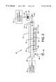
- FIG. 1illustrates one method and apparatus according to the present invention for Metal Oxide Chemical Vapor Deposition on a substrate surface.
- a downflow reactor 10 apparatusis incorporated and utilized for Metal Oxide Chemical Vapor Deposition (MOCVD) upon the upper surface of a substrate 12 positioned central to the downflow reactor 10 .
- the downflow reactor 10is a cold wall vacuum reactor comprising a vertically oriented vessel 13 having an interior chamber 15 defined by a surrounding vessel wall 14 about and to which related structure and devices are attached or extend therefrom.
- a gas inlet 16 for receiving a gas from a Mass Flow Controller (MFC), not illustrated,is located at the upper region of the vessel 13 .
- MFCMass Flow Controller
- a gas outlet 18Opposing the gas inlet 16 and located at the lower region of the vessel 13 is a gas outlet 18 to which a metering valve 20 is attached for control of the gases transitting through the vessel 14 .
- a thermally conductive chuck 22 of large mass and having a substrate holding portionis utilized to hold the wafer or substrate 12 during processing.
- the entire chuck 22is located centrally within the interior chamber 15 of the vessel 13 .
- a suitable resistance heater 25 and one or more thermocouples 24 a - 24 nare embedded in the chuck 22 for heating the chuck 22 and for monitoring and controlling the temperature across the chuck 22 .
- the large mass of the chuck 22is conducive to achieving uniform and even temperature distribution across the chuck 22 to enhance boundary layer control.
- the chuck 22normally remains static (stationary) during the deposition process, but is arranged so that, if necessary or desired, it can be vibrated or can be oscillated at a low frequency either vertically or horizontally, or in the alternative simultaneously both vertically and horizontally, to assist in control of reduced boundary layer thickness and to contribute to boundary layer uniformity control.
- a chamber 26is located at and attached to the gas inlet 16 at the upper region of the vessel 13 .
- An isolation bellows 28is located in the chamber 26 .
- An inlet 30is attached to the chamber 26 to receive a disturbance input from a primary disturbance source 32 .
- the primary disturbance source 32introduces periodic disturbances in wave form into the interior chamber 15 of the vessel 13 of the downflow reactor 10 through the inlet 30 , the chamber 26 , the isolation bellows 28 and the gas inlet 16 .
- the periodic disturbances emanating from the primary disturbance source 32can be provided by a device such as, but not limited to, a pneumatic oscillator which provides a sinusoidal disturbance.
- One or more transducers 33 and alternate disturbance sources 34are attached to the vessel wall 14 and either acts alone for imparting a disturbance in wave form into the interior chamber 15 of the vessel 13 of the downflow reactor 10 or acts in concert with the primary disturbance source 32 to impart multiple or reinforced disturbances into the interior chamber 15 of the vessel 13 of the downflow reactor 10 .
- Both the primary and the alternate disturbance sources 32 and 34can include, but are not limited to, a pneumatic oscillator, a speaker, a piezo or other electromagnetic device, or a bellows with a pneumatic source, each of which generates an appropriate disturbance.
- FIG. 2illustrates another method and apparatus according to the present invention for Metal Oxide Chemical Vapor Deposition on a substrate surface.
- a crossflow reactor 40 apparatusis incorporated and utilized for Metal Oxide Chemical Vapor Deposition (MOCVD) upon the upper surface of a substrate 42 positioned central to the crossflow reactor 40 .
- the crossflow reactor 40is a cold wall vacuum reactor comprising a horizontally oriented vessel 43 having an interior chamber 45 defined by a surrounding vessel wall 44 about and to which related structure and devices are attached or extend therefrom.
- a gas inlet 46 for receiving a gas from a Mass Flow Controller (MFC), not illustrated,is located at one end of the vessel 13 .
- MFCMass Flow Controller
- a gas outlet 48Opposing the gas inlet 46 and located at the opposing end of the vessel 43 is a gas outlet 48 to which a metering valve 50 is attached for control of the gases transitting through the vessel 44 .
- a thermally conductive chuck 52 of large mass and having a substrate holding portionis utilized to hold the wafer or substrate 42 during processing.
- the chuck 52is centrally located externally along the vessel 43 and extends slightly through the vessel wall 44 to place the substrate 42 carried thereby within the interior chamber 45 in a position substantially flush with the interior surface of the vessel wall 44 in order to reduce the volume of gas required and to attain good laminar flow.
- a suitable resistance heater 55 and one or more thermocouples 54 a - 54 nare embedded in the chuck 52 for heating the chuck 52 and for monitoring and controlling the temperature across the chuck 52 .
- the large mass of the chuck 52is conducive to achieving uniform and even temperature distribution across the chuck 52 to enhance boundary layer control.
- One or more transducers 56 and primary disturbance sources 58are attached to the end or other suitable site on the vessel wall 44 to provide periodic disturbance in wave form into the interior chamber 45 of the vessel 43 of the crossflow reactor 40 .
- the periodic disturbances emanating from the primary disturbance source 58can be provided by a device such as, but not limited to, a pneumatic oscillator which provides a sinusoidal disturbance.
- An alternate disturbance source 62is located at the end of the vessel 43 whereat the gas inlet 46 is located; and an additional transducer 70 for providing yet another disturbance source is located along the vessel 43 on the vessel wall 44 .
- a chamber 64is located at and attached to the gas inlet 46 at the end of the vessel 43 .
- An isolation bellows 66is located in the chamber 64 .
- An inlet 68is attached to the chamber 64 to receive a disturbance input from the alternate disturbance source 62 .
- the alternate disturbance source 62introduces periodic disturbances in wave form into the interior chamber 45 of the vessel 43 of the crossflow reactor 40 through the inlet 68 , the chamber 64 , the isolation bellows 66 and the gas inlet 46 .
- Both the primary and the alternate disturbance sources 58 and 62 , respectively, and the additional transducer 70can include, but are not limited to, a pneumatic oscillator, a speaker, a piezo or other electromagnetic device, or a bellows with a pneumatic source, each of which generates an appropriate disturbance.
- the primary disturbance source 58 and transducer 56can be used as a stand-alone device for introduction of periodic disturbance into the interior chamber 45 , but in the alternative, the additional transducer 70 located on the vessel wall 44 can be employed simultaneously.
- the alternate disturbance source 62including the delivery components, can be used as a stand-alone device for introduction of periodic disturbance into the interior chamber 45 , but in the alternative, the additional transducer 70 located on the vessel wall 44 can be employed simultaneously.
- all disturbance sourcesthat is, the primary disturbance source 58 and transducer 56 , the alternate disturbance source 62 , and the additional transducer 70 , can be utilized simultaneously. Other combinations incorporating the use of one or more disturbance sources, transducers and the like are also included within the scope of the invention.
Landscapes
- Chemical & Material Sciences (AREA)
- General Chemical & Material Sciences (AREA)
- Chemical Kinetics & Catalysis (AREA)
- Engineering & Computer Science (AREA)
- Materials Engineering (AREA)
- Mechanical Engineering (AREA)
- Metallurgy (AREA)
- Organic Chemistry (AREA)
- Physics & Mathematics (AREA)
- Acoustics & Sound (AREA)
- Chemical Vapour Deposition (AREA)
Abstract
Description
| METHOD AND APPARATUS FOR METAL OXIDE CHEMICAL |
| VAPOR DEPOSITION ON A SUBSTRATE SURFACE |
| PARTS LIST |
| 10 | |||
| 12 | |||
| 13 | |||
| 14 | |||
| 15 | |||
| 16 | |||
| 18 | |||
| 20 | |||
| 22 | |||
| 24a- | thermocouples | ||
| 25 | |||
| 26 | |||
| 28 | isolation bellows | ||
| 29 | |||
| 30 | |||
| 32 | |||
| source | |||
| 33 | |||
| 34 | |||
| source | |||
| 40 | |||
| 42 | |||
| 43 | |||
| 44 | |||
| 45 | |||
| 46 | |||
| 48 | |||
| 50 | |||
| 52 | |||
| 54a- | thermocouples | ||
| 55 | |||
| 56 | |||
| 58 | |||
| source | |||
| 60 | |||
| 62 | |||
| source | |||
| 64 | |||
| 66 | isolation bellows | ||
| 68 | |||
| 70 | transducer | ||
Claims (29)
Priority Applications (5)
| Application Number | Priority Date | Filing Date | Title |
|---|---|---|---|
| US09/272,036US6231933B1 (en) | 1999-03-18 | 1999-03-18 | Method and apparatus for metal oxide chemical vapor deposition on a substrate surface |
| US09/352,080US6261373B1 (en) | 1999-03-18 | 1999-07-14 | Method and apparatus for metal oxide chemical vapor deposition on a substrate surface |
| PCT/US2000/005385WO2000054893A1 (en) | 1999-03-18 | 2000-02-28 | Method and apparatus for metal oxide chemical vapor deposition on a substrate surface |
| EP00915975AEP1189706A1 (en) | 1999-03-18 | 2000-02-28 | Method and apparatus for metal oxide chemical vapor deposition on a substrate surface |
| JP2000604957AJP2002539327A (en) | 1999-03-18 | 2000-02-28 | Method and apparatus for forming a metal oxide on a substrate surface by chemical vapor deposition |
Applications Claiming Priority (1)
| Application Number | Priority Date | Filing Date | Title |
|---|---|---|---|
| US09/272,036US6231933B1 (en) | 1999-03-18 | 1999-03-18 | Method and apparatus for metal oxide chemical vapor deposition on a substrate surface |
Related Child Applications (1)
| Application Number | Title | Priority Date | Filing Date |
|---|---|---|---|
| US09/352,080DivisionUS6261373B1 (en) | 1999-03-18 | 1999-07-14 | Method and apparatus for metal oxide chemical vapor deposition on a substrate surface |
Publications (1)
| Publication Number | Publication Date |
|---|---|
| US6231933B1true US6231933B1 (en) | 2001-05-15 |
Family
ID=23038134
Family Applications (2)
| Application Number | Title | Priority Date | Filing Date |
|---|---|---|---|
| US09/272,036Expired - Fee RelatedUS6231933B1 (en) | 1999-03-18 | 1999-03-18 | Method and apparatus for metal oxide chemical vapor deposition on a substrate surface |
| US09/352,080Expired - Fee RelatedUS6261373B1 (en) | 1999-03-18 | 1999-07-14 | Method and apparatus for metal oxide chemical vapor deposition on a substrate surface |
Family Applications After (1)
| Application Number | Title | Priority Date | Filing Date |
|---|---|---|---|
| US09/352,080Expired - Fee RelatedUS6261373B1 (en) | 1999-03-18 | 1999-07-14 | Method and apparatus for metal oxide chemical vapor deposition on a substrate surface |
Country Status (4)
| Country | Link |
|---|---|
| US (2) | US6231933B1 (en) |
| EP (1) | EP1189706A1 (en) |
| JP (1) | JP2002539327A (en) |
| WO (1) | WO2000054893A1 (en) |
Cited By (4)
| Publication number | Priority date | Publication date | Assignee | Title |
|---|---|---|---|---|
| US20060211271A1 (en)* | 2005-03-17 | 2006-09-21 | Weigel Scott J | Aerosol misted deposition of low dielectric organosilicate films |
| US20090168837A1 (en)* | 2007-12-19 | 2009-07-02 | Von Ardenne Anlagentechnik Gmbh | Method for the temperature measurement of substrates, and vacuum processing apparatus |
| US9312200B1 (en)* | 2013-03-13 | 2016-04-12 | Amazon Technologies, Inc. | Solid structures for thermal management |
| US9748113B2 (en) | 2015-07-30 | 2017-08-29 | Veeco Intruments Inc. | Method and apparatus for controlled dopant incorporation and activation in a chemical vapor deposition system |
Families Citing this family (8)
| Publication number | Priority date | Publication date | Assignee | Title |
|---|---|---|---|---|
| AU2002242923A1 (en)* | 2001-03-27 | 2002-10-08 | Apit Corp. Sa | Plasma surface treatment method and device for carrying out said method |
| US7524532B2 (en)* | 2002-04-22 | 2009-04-28 | Aixtron Ag | Process for depositing thin layers on a substrate in a process chamber of adjustable height |
| US20040222210A1 (en)* | 2003-05-08 | 2004-11-11 | Hongy Lin | Multi-zone ceramic heating system and method of manufacture thereof |
| AU2005270587B2 (en) | 2004-08-13 | 2009-11-19 | Sanovo Biosecurity A/S | Method and device for enhancing a process involving a solid object and a gas |
| US20060236931A1 (en)* | 2005-04-25 | 2006-10-26 | Varian Semiconductor Equipment Associates, Inc. | Tilted Plasma Doping |
| PL2153704T3 (en)* | 2007-05-11 | 2018-06-29 | Force Technology | Enhancing plasma surface modification using high intensity and high power ultrasonic acoustic waves |
| KR100938358B1 (en)* | 2007-11-22 | 2010-01-22 | 에이피시스템 주식회사 | Substrate rocking device for rapid heat treatment |
| JP6372709B2 (en)* | 2016-04-20 | 2018-08-15 | 信越半導体株式会社 | Epitaxial wafer manufacturing method |
Citations (15)
| Publication number | Priority date | Publication date | Assignee | Title |
|---|---|---|---|---|
| US4705700A (en) | 1985-05-31 | 1987-11-10 | The Furukawa Electric Co., Ltd. | Chemical vapor deposition method for the thin film of semiconductor |
| JPH01317112A (en)* | 1988-06-15 | 1989-12-21 | Sumitomo Electric Ind Ltd | High strength polycrystalline diamond and its manufacturing method |
| US4916089A (en) | 1987-09-04 | 1990-04-10 | Stichting Katholieke Universiteit | Process for the epitaxial production of semiconductor stock material |
| US4969416A (en) | 1986-07-03 | 1990-11-13 | Emcore, Inc. | Gas treatment apparatus and method |
| US5037775A (en) | 1988-11-30 | 1991-08-06 | Mcnc | Method for selectively depositing single elemental semiconductor material on substrates |
| JPH05144657A (en)* | 1991-11-25 | 1993-06-11 | Matsushita Electric Ind Co Ltd | Method for manufacturing soft magnetic ferrite thin film |
| US5273932A (en) | 1988-08-15 | 1993-12-28 | Nippon Telegraph & Telephone Corp. | Method for forming semiconductor thin films where an argon laser is used to suppress crystal growth |
| US5288327A (en) | 1992-03-12 | 1994-02-22 | Bell Communications Research, Inc. | Deflected flow in chemical vapor deposition cell |
| JPH06283449A (en)* | 1993-03-24 | 1994-10-07 | Tokyo Electron Ltd | Evacuation and vacuum equipment |
| US5365877A (en) | 1990-03-20 | 1994-11-22 | Kabushiki Kaisha Toshiba | Method of growing semiconductor in vapor phase |
| US5433169A (en) | 1990-10-25 | 1995-07-18 | Nichia Chemical Industries, Ltd. | Method of depositing a gallium nitride-based III-V group compound semiconductor crystal layer |
| JPH08115911A (en)* | 1994-08-25 | 1996-05-07 | Sony Corp | Manufacture of semiconductor device |
| US5755878A (en) | 1994-10-25 | 1998-05-26 | Shin-Etsu Handotai Co., Ltd. | Method for vapor phase growth |
| US5814561A (en) | 1997-02-14 | 1998-09-29 | Jackson; Paul D. | Substrate carrier having a streamlined shape and method for thin film formation |
| US5998303A (en)* | 1996-03-19 | 1999-12-07 | Sony Corporation | Semiconductor device making method |
Family Cites Families (5)
| Publication number | Priority date | Publication date | Assignee | Title |
|---|---|---|---|---|
| JPS61295461A (en)* | 1985-06-21 | 1986-12-26 | Sanyo Electric Co Ltd | Hot water supplier |
| JPH01298169A (en)* | 1988-05-27 | 1989-12-01 | Tokyo Electron Ltd | Film formation |
| EP0628644B1 (en)* | 1993-05-27 | 2003-04-02 | Applied Materials, Inc. | Improvements in or relating to susceptors suitable for use in chemical vapour deposition devices |
| US6099648A (en)* | 1997-08-06 | 2000-08-08 | Applied Materials, Inc. | Domed wafer reactor vessel window with reduced stress at atmospheric and above atmospheric pressures |
| US6013319A (en)* | 1998-04-28 | 2000-01-11 | Dietze; Gerald R. | Method and apparatus for increasing deposition quality of a chemical vapor deposition system |
- 1999
- 1999-03-18USUS09/272,036patent/US6231933B1/ennot_activeExpired - Fee Related
- 1999-07-14USUS09/352,080patent/US6261373B1/ennot_activeExpired - Fee Related
- 2000
- 2000-02-28EPEP00915975Apatent/EP1189706A1/ennot_activeWithdrawn
- 2000-02-28WOPCT/US2000/005385patent/WO2000054893A1/ennot_activeApplication Discontinuation
- 2000-02-28JPJP2000604957Apatent/JP2002539327A/enactivePending
Patent Citations (15)
| Publication number | Priority date | Publication date | Assignee | Title |
|---|---|---|---|---|
| US4705700A (en) | 1985-05-31 | 1987-11-10 | The Furukawa Electric Co., Ltd. | Chemical vapor deposition method for the thin film of semiconductor |
| US4969416A (en) | 1986-07-03 | 1990-11-13 | Emcore, Inc. | Gas treatment apparatus and method |
| US4916089A (en) | 1987-09-04 | 1990-04-10 | Stichting Katholieke Universiteit | Process for the epitaxial production of semiconductor stock material |
| JPH01317112A (en)* | 1988-06-15 | 1989-12-21 | Sumitomo Electric Ind Ltd | High strength polycrystalline diamond and its manufacturing method |
| US5273932A (en) | 1988-08-15 | 1993-12-28 | Nippon Telegraph & Telephone Corp. | Method for forming semiconductor thin films where an argon laser is used to suppress crystal growth |
| US5037775A (en) | 1988-11-30 | 1991-08-06 | Mcnc | Method for selectively depositing single elemental semiconductor material on substrates |
| US5365877A (en) | 1990-03-20 | 1994-11-22 | Kabushiki Kaisha Toshiba | Method of growing semiconductor in vapor phase |
| US5433169A (en) | 1990-10-25 | 1995-07-18 | Nichia Chemical Industries, Ltd. | Method of depositing a gallium nitride-based III-V group compound semiconductor crystal layer |
| JPH05144657A (en)* | 1991-11-25 | 1993-06-11 | Matsushita Electric Ind Co Ltd | Method for manufacturing soft magnetic ferrite thin film |
| US5288327A (en) | 1992-03-12 | 1994-02-22 | Bell Communications Research, Inc. | Deflected flow in chemical vapor deposition cell |
| JPH06283449A (en)* | 1993-03-24 | 1994-10-07 | Tokyo Electron Ltd | Evacuation and vacuum equipment |
| JPH08115911A (en)* | 1994-08-25 | 1996-05-07 | Sony Corp | Manufacture of semiconductor device |
| US5755878A (en) | 1994-10-25 | 1998-05-26 | Shin-Etsu Handotai Co., Ltd. | Method for vapor phase growth |
| US5998303A (en)* | 1996-03-19 | 1999-12-07 | Sony Corporation | Semiconductor device making method |
| US5814561A (en) | 1997-02-14 | 1998-09-29 | Jackson; Paul D. | Substrate carrier having a streamlined shape and method for thin film formation |
Non-Patent Citations (1)
| Title |
|---|
| Hermann Schlichting, Boundary Layer Theory, Seventh Edition, Chapter V, Section b, and Chapter XV, Sections a and e. (No date available). |
Cited By (7)
| Publication number | Priority date | Publication date | Assignee | Title |
|---|---|---|---|---|
| US20060211271A1 (en)* | 2005-03-17 | 2006-09-21 | Weigel Scott J | Aerosol misted deposition of low dielectric organosilicate films |
| US7446055B2 (en) | 2005-03-17 | 2008-11-04 | Air Products And Chemicals, Inc. | Aerosol misted deposition of low dielectric organosilicate films |
| US20090168837A1 (en)* | 2007-12-19 | 2009-07-02 | Von Ardenne Anlagentechnik Gmbh | Method for the temperature measurement of substrates, and vacuum processing apparatus |
| US8070356B2 (en)* | 2007-12-19 | 2011-12-06 | Von Ardenne Anlagentechnik Gmbh | Method for the temperature measurement of substrates, and vacuum processing apparatus |
| US9312200B1 (en)* | 2013-03-13 | 2016-04-12 | Amazon Technologies, Inc. | Solid structures for thermal management |
| US9748113B2 (en) | 2015-07-30 | 2017-08-29 | Veeco Intruments Inc. | Method and apparatus for controlled dopant incorporation and activation in a chemical vapor deposition system |
| DE112016003443T5 (en) | 2015-07-30 | 2018-04-19 | Veeco Instruments Inc. | Method and apparatus for controlled introduction and activation of dopants in a chemical vapor deposition system |
Also Published As
| Publication number | Publication date |
|---|---|
| US6261373B1 (en) | 2001-07-17 |
| WO2000054893A1 (en) | 2000-09-21 |
| JP2002539327A (en) | 2002-11-19 |
| EP1189706A1 (en) | 2002-03-27 |
Similar Documents
| Publication | Publication Date | Title |
|---|---|---|
| US6231933B1 (en) | Method and apparatus for metal oxide chemical vapor deposition on a substrate surface | |
| US9396909B2 (en) | Gas dispersion apparatus | |
| KR100791419B1 (en) | Showerhead with reduced contact area | |
| JP4536662B2 (en) | Gas processing apparatus and heat dissipation method | |
| US5735960A (en) | Apparatus and method to increase gas residence time in a reactor | |
| US20080283086A1 (en) | Substrate processing apparatus and cleaning method therefor | |
| KR20140031907A (en) | Apparatus for deposition of materials on a substrate | |
| EP3223301B1 (en) | Film-forming apparatus | |
| Pawlowski et al. | Fundamental models of the metalorganic vapor-phase epitaxy of gallium nitride and their use in reactor design | |
| KR20040032958A (en) | Process for controlling thin film uniformity and products produced thereby | |
| CN115110061A (en) | Temperature controlled reaction chamber | |
| TW200847243A (en) | Apparatus and method for forming film | |
| US20190032244A1 (en) | Chemical vapor deposition system | |
| KR102179974B1 (en) | Apparatus and method for forming a nitride coating layer | |
| KR20140018148A (en) | Method and apparatus of forming compound semiconductor film | |
| JP2003086516A (en) | Susceptor, CVD device, film forming method, and semiconductor device | |
| JP2733535B2 (en) | Semiconductor thin film vapor deposition equipment | |
| KR101942536B1 (en) | Method for fabrication silicon carbide epi wafer | |
| JPS59159980A (en) | Vapor phase growth equipment | |
| JPS607378B2 (en) | CVD equipment | |
| JP2003201566A (en) | Chemical vapor deposition equipment | |
| GB2395492A (en) | Improvements in deposition methods for the production of semiconductors | |
| JPS6338581A (en) | Functional deposited film forming device | |
| JP4682001B2 (en) | Crystal thin film manufacturing equipment | |
| JPS6136698B2 (en) |
Legal Events
| Date | Code | Title | Description |
|---|---|---|---|
| AS | Assignment | Owner name:PRIMAXX, INC., PENNSYLVANIA Free format text:ASSIGNMENT OF ASSIGNORS INTEREST;ASSIGNOR:GRANT, ROBERT W.;REEL/FRAME:009853/0811 Effective date:19990317 | |
| AS | Assignment | Owner name:SAND HILL CAPITAL II, LP, CALIFORNIA Free format text:SECURITY INTEREST;ASSIGNOR:PRIMAXX, INC.;REEL/FRAME:011390/0292 Effective date:20001031 | |
| AS | Assignment | Owner name:FB COMMERCIAL FINANCE, INC., MISSOURI Free format text:SECURITY AGREEMENT;ASSIGNORS:SAND HILL CAPITAL II,L.P.;SAND HILL CAPITAL II Q, L.P.;SAND HILL CAPITAL, LLC;REEL/FRAME:011731/0841 Effective date:20001211 | |
| AS | Assignment | Owner name:SAND HILL CAPITAL II, L.P., CALIFORNIA Free format text:REASSIGNMENT AND RELEASE OF SECURITY INTEREST;ASSIGNOR:FB COMMERCIAL FINANCE, INC.;REEL/FRAME:012875/0384 Effective date:20020429 Owner name:SAND HILL CAPITAL IIQ, L.P., CALIFORNIA Free format text:REASSIGNMENT AND RELEASE OF SECURITY INTEREST;ASSIGNOR:FB COMMERCIAL FINANCE, INC.;REEL/FRAME:012875/0384 Effective date:20020429 Owner name:SAN HILL CAPITAL, L.L.C., CALIFORNIA Free format text:REASSIGNMENT AND RELEASE OF SECURITY INTEREST;ASSIGNOR:FB COMMERCIAL FINANCE, INC.;REEL/FRAME:012875/0384 Effective date:20020429 | |
| REMI | Maintenance fee reminder mailed | ||
| LAPS | Lapse for failure to pay maintenance fees | ||
| STCH | Information on status: patent discontinuation | Free format text:PATENT EXPIRED DUE TO NONPAYMENT OF MAINTENANCE FEES UNDER 37 CFR 1.362 | |
| FP | Lapsed due to failure to pay maintenance fee | Effective date:20050515 |