US6230720B1 - Single-operation method of cleaning semiconductors after final polishing - Google Patents
Single-operation method of cleaning semiconductors after final polishingDownload PDFInfo
- Publication number
- US6230720B1 US6230720B1US09/606,728US60672800AUS6230720B1US 6230720 B1US6230720 B1US 6230720B1US 60672800 AUS60672800 AUS 60672800AUS 6230720 B1US6230720 B1US 6230720B1
- Authority
- US
- United States
- Prior art keywords
- set forth
- semiconductor wafer
- concentration
- cleaning solution
- wafer
- Prior art date
- Legal status (The legal status is an assumption and is not a legal conclusion. Google has not performed a legal analysis and makes no representation as to the accuracy of the status listed.)
- Expired - Fee Related
Links
- 238000000034methodMethods0.000titleclaimsabstractdescription117
- 238000004140cleaningMethods0.000titleclaimsabstractdescription103
- 239000004065semiconductorSubstances0.000titleclaimsabstractdescription67
- 238000005498polishingMethods0.000titleabstractdescription17
- XLYOFNOQVPJJNP-UHFFFAOYSA-NwaterChemical compoundOXLYOFNOQVPJJNP-UHFFFAOYSA-N0.000claimsabstractdescription93
- 230000008569processEffects0.000claimsabstractdescription79
- 239000000243solutionSubstances0.000claimsabstractdescription76
- 239000002245particleSubstances0.000claimsabstractdescription64
- 239000000356contaminantSubstances0.000claimsabstractdescription54
- 239000008367deionised waterSubstances0.000claimsabstractdescription31
- 229910021641deionized waterInorganic materials0.000claimsabstractdescription31
- 229910052751metalInorganic materials0.000claimsabstractdescription29
- 239000002184metalSubstances0.000claimsabstractdescription29
- 238000001035dryingMethods0.000claimsabstractdescription22
- 230000002378acidificating effectEffects0.000claimsabstractdescription20
- 239000007864aqueous solutionSubstances0.000claimsabstractdescription16
- 239000007800oxidant agentSubstances0.000claimsabstractdescription16
- OKTJSMMVPCPJKN-UHFFFAOYSA-NCarbonChemical compound[C]OKTJSMMVPCPJKN-UHFFFAOYSA-N0.000claimsabstractdescription8
- 229910052799carbonInorganic materials0.000claimsabstractdescription8
- 229910001868waterInorganic materials0.000claimsdescription62
- CBENFWSGALASAD-UHFFFAOYSA-NOzoneChemical compound[O-][O+]=OCBENFWSGALASAD-UHFFFAOYSA-N0.000claimsdescription44
- MHAJPDPJQMAIIY-UHFFFAOYSA-NHydrogen peroxideChemical compoundOOMHAJPDPJQMAIIY-UHFFFAOYSA-N0.000claimsdescription43
- 239000002253acidSubstances0.000claimsdescription29
- VHUUQVKOLVNVRT-UHFFFAOYSA-NAmmonium hydroxideChemical compound[NH4+].[OH-]VHUUQVKOLVNVRT-UHFFFAOYSA-N0.000claimsdescription21
- 125000004432carbon atomChemical groupC*0.000claimsdescription21
- 125000004429atomChemical group0.000claimsdescription19
- 150000002739metalsChemical class0.000claimsdescription18
- XUIMIQQOPSSXEZ-UHFFFAOYSA-NSiliconChemical compound[Si]XUIMIQQOPSSXEZ-UHFFFAOYSA-N0.000claimsdescription16
- 239000010703siliconSubstances0.000claimsdescription16
- 229910052710siliconInorganic materials0.000claimsdescription16
- 150000002894organic compoundsChemical class0.000claimsdescription15
- 239000000908ammonium hydroxideSubstances0.000claimsdescription12
- 230000003746surface roughnessEffects0.000claimsdescription12
- 238000005530etchingMethods0.000claimsdescription8
- VEXZGXHMUGYJMC-UHFFFAOYSA-NHydrochloric acidChemical compoundClVEXZGXHMUGYJMC-UHFFFAOYSA-N0.000claimsdescription7
- XEEYBQQBJWHFJM-UHFFFAOYSA-NIronChemical compound[Fe]XEEYBQQBJWHFJM-UHFFFAOYSA-N0.000claimsdescription6
- KRKNYBCHXYNGOX-UHFFFAOYSA-Ncitric acidChemical compoundOC(=O)CC(O)(C(O)=O)CC(O)=OKRKNYBCHXYNGOX-UHFFFAOYSA-N0.000claimsdescription6
- GRYLNZFGIOXLOG-UHFFFAOYSA-NNitric acidChemical compoundO[N+]([O-])=OGRYLNZFGIOXLOG-UHFFFAOYSA-N0.000claimsdescription3
- HCHKCACWOHOZIP-UHFFFAOYSA-NZincChemical compound[Zn]HCHKCACWOHOZIP-UHFFFAOYSA-N0.000claimsdescription3
- 229910052782aluminiumInorganic materials0.000claimsdescription3
- XAGFODPZIPBFFR-UHFFFAOYSA-NaluminiumChemical compound[Al]XAGFODPZIPBFFR-UHFFFAOYSA-N0.000claimsdescription3
- 230000015556catabolic processEffects0.000claimsdescription3
- 239000003153chemical reaction reagentSubstances0.000claimsdescription3
- 238000006731degradation reactionMethods0.000claimsdescription3
- -1hydroxyl ionsChemical class0.000claimsdescription3
- 229910052742ironInorganic materials0.000claimsdescription3
- 239000000203mixtureSubstances0.000claimsdescription3
- 229910017604nitric acidInorganic materials0.000claimsdescription3
- 229910052725zincInorganic materials0.000claimsdescription3
- 239000011701zincSubstances0.000claimsdescription3
- 230000001590oxidative effectEffects0.000abstractdescription11
- 230000009471actionEffects0.000abstractdescription3
- 235000012431wafersNutrition0.000description166
- 239000012670alkaline solutionSubstances0.000description17
- KFZMGEQAYNKOFK-UHFFFAOYSA-NIsopropanolChemical compoundCC(C)OKFZMGEQAYNKOFK-UHFFFAOYSA-N0.000description14
- 235000011114ammonium hydroxideNutrition0.000description10
- 238000004519manufacturing processMethods0.000description10
- VYPSYNLAJGMNEJ-UHFFFAOYSA-NSilicium dioxideChemical compoundO=[Si]=OVYPSYNLAJGMNEJ-UHFFFAOYSA-N0.000description8
- 238000011109contaminationMethods0.000description7
- 230000001965increasing effectEffects0.000description7
- 238000011282treatmentMethods0.000description7
- 238000001514detection methodMethods0.000description6
- 150000002500ionsChemical class0.000description6
- 229910052814silicon oxideInorganic materials0.000description6
- LFQSCWFLJHTTHZ-UHFFFAOYSA-NEthanolChemical compoundCCOLFQSCWFLJHTTHZ-UHFFFAOYSA-N0.000description5
- 230000007423decreaseEffects0.000description5
- 238000005507sprayingMethods0.000description5
- KRHYYFGTRYWZRS-UHFFFAOYSA-NFluoraneChemical compoundFKRHYYFGTRYWZRS-UHFFFAOYSA-N0.000description4
- 230000003647oxidationEffects0.000description4
- 238000007254oxidation reactionMethods0.000description4
- 239000002994raw materialSubstances0.000description4
- WGTYBPLFGIVFAS-UHFFFAOYSA-Mtetramethylammonium hydroxideChemical compound[OH-].C[N+](C)(C)CWGTYBPLFGIVFAS-UHFFFAOYSA-M0.000description4
- MUBZPKHOEPUJKR-UHFFFAOYSA-NOxalic acidChemical compoundOC(=O)C(O)=OMUBZPKHOEPUJKR-UHFFFAOYSA-N0.000description3
- 238000010438heat treatmentMethods0.000description3
- 239000000463materialSubstances0.000description3
- 239000002699waste materialSubstances0.000description3
- OQSOTSIYXPYTRE-YDOWWZDFSA-N(+)-sesamin dicatecholChemical compoundC1=C(O)C(O)=CC=C1[C@@H]1[C@@H](CO[C@@H]2C=3C=C(O)C(O)=CC=3)[C@@H]2CO1OQSOTSIYXPYTRE-YDOWWZDFSA-N0.000description2
- QGZKDVFQNNGYKY-UHFFFAOYSA-NAmmoniaChemical compoundNQGZKDVFQNNGYKY-UHFFFAOYSA-N0.000description2
- QAOWNCQODCNURD-UHFFFAOYSA-NSulfuric acidChemical compoundOS(O)(=O)=OQAOWNCQODCNURD-UHFFFAOYSA-N0.000description2
- 239000003929acidic solutionSubstances0.000description2
- 230000008901benefitEffects0.000description2
- 230000008859changeEffects0.000description2
- 230000003749cleanlinessEffects0.000description2
- 150000001875compoundsChemical class0.000description2
- 238000001816coolingMethods0.000description2
- 230000003247decreasing effectEffects0.000description2
- 238000005516engineering processMethods0.000description2
- 230000005661hydrophobic surfaceEffects0.000description2
- 239000013618particulate matterSubstances0.000description2
- 238000005201scrubbingMethods0.000description2
- 239000004094surface-active agentSubstances0.000description2
- 238000012360testing methodMethods0.000description2
- QGZKDVFQNNGYKY-UHFFFAOYSA-OAmmoniumChemical compound[NH4+]QGZKDVFQNNGYKY-UHFFFAOYSA-O0.000description1
- IJGRMHOSHXDMSA-UHFFFAOYSA-NAtomic nitrogenChemical compoundN#NIJGRMHOSHXDMSA-UHFFFAOYSA-N0.000description1
- 241000252506CharaciformesSpecies0.000description1
- NINIDFKCEFEMDL-UHFFFAOYSA-NSulfurChemical compound[S]NINIDFKCEFEMDL-UHFFFAOYSA-N0.000description1
- 125000005210alkyl ammonium groupChemical group0.000description1
- 229910021529ammoniaInorganic materials0.000description1
- 238000001636atomic emission spectroscopyMethods0.000description1
- 238000004630atomic force microscopyMethods0.000description1
- 230000033228biological regulationEffects0.000description1
- 238000007664blowingMethods0.000description1
- ZCDOYSPFYFSLEW-UHFFFAOYSA-Nchromate(2-)Chemical compound[O-][Cr]([O-])(=O)=OZCDOYSPFYFSLEW-UHFFFAOYSA-N0.000description1
- 229910001873dinitrogenInorganic materials0.000description1
- 230000007613environmental effectEffects0.000description1
- 238000001914filtrationMethods0.000description1
- 238000004817gas chromatographyMethods0.000description1
- 238000000227grindingMethods0.000description1
- 230000006872improvementEffects0.000description1
- 230000001939inductive effectEffects0.000description1
- 125000001449isopropyl groupChemical group[H]C([H])([H])C([H])(*)C([H])([H])[H]0.000description1
- 238000004949mass spectrometryMethods0.000description1
- 235000006408oxalic acidNutrition0.000description1
- VLTRZXGMWDSKGL-UHFFFAOYSA-MperchlorateInorganic materials[O-]Cl(=O)(=O)=OVLTRZXGMWDSKGL-UHFFFAOYSA-M0.000description1
- VLTRZXGMWDSKGL-UHFFFAOYSA-Nperchloric acidChemical compoundOCl(=O)(=O)=OVLTRZXGMWDSKGL-UHFFFAOYSA-N0.000description1
- JRKICGRDRMAZLK-UHFFFAOYSA-Nperoxydisulfuric acidChemical compoundOS(=O)(=O)OOS(O)(=O)=OJRKICGRDRMAZLK-UHFFFAOYSA-N0.000description1
- 238000009428plumbingMethods0.000description1
- 238000007788rougheningMethods0.000description1
- 239000000377silicon dioxideSubstances0.000description1
- 239000007921spraySubstances0.000description1
- 229910052717sulfurInorganic materials0.000description1
- 239000011593sulfurSubstances0.000description1
- 229940073455tetraethylammonium hydroxideDrugs0.000description1
- LRGJRHZIDJQFCL-UHFFFAOYSA-Mtetraethylazanium;hydroxideChemical compound[OH-].CC[N+](CC)(CC)CCLRGJRHZIDJQFCL-UHFFFAOYSA-M0.000description1
- 239000012498ultrapure waterSubstances0.000description1
- 238000004506ultrasonic cleaningMethods0.000description1
- 238000005406washingMethods0.000description1
Images


Classifications
- H—ELECTRICITY
- H01—ELECTRIC ELEMENTS
- H01L—SEMICONDUCTOR DEVICES NOT COVERED BY CLASS H10
- H01L21/00—Processes or apparatus adapted for the manufacture or treatment of semiconductor or solid state devices or of parts thereof
- H01L21/02—Manufacture or treatment of semiconductor devices or of parts thereof
- H01L21/02041—Cleaning
- H01L21/02043—Cleaning before device manufacture, i.e. Begin-Of-Line process
- H01L21/02052—Wet cleaning only
- Y—GENERAL TAGGING OF NEW TECHNOLOGICAL DEVELOPMENTS; GENERAL TAGGING OF CROSS-SECTIONAL TECHNOLOGIES SPANNING OVER SEVERAL SECTIONS OF THE IPC; TECHNICAL SUBJECTS COVERED BY FORMER USPC CROSS-REFERENCE ART COLLECTIONS [XRACs] AND DIGESTS
- Y10—TECHNICAL SUBJECTS COVERED BY FORMER USPC
- Y10S—TECHNICAL SUBJECTS COVERED BY FORMER USPC CROSS-REFERENCE ART COLLECTIONS [XRACs] AND DIGESTS
- Y10S134/00—Cleaning and liquid contact with solids
- Y10S134/902—Semiconductor wafer
Definitions
- the present inventionrelates generally to the cleaning of semiconductors, and more particularly to the cleaning of semiconductor (e.g., silicon) wafers after final polishing.
- semiconductore.g., silicon
- the manufacture of semiconductor wafersrequires numerous processing operations including growing an ingot, slicing, lapping, grinding, etching, polishing and cleaning.
- the final polishing operationreduces the surface roughness of the wafer to a level acceptable for semiconductor device manufacturers (e.g., about 0.02 nm to about 0.5 nm based upon Atomic Force Microscopy of a 10 ⁇ m ⁇ 10 ⁇ m field of view) while it increases the total thickness variation of the wafer by about 0.1 to about 1.5 ⁇ m (e.g., current detection limits are about 0.01 ⁇ m, for conventional capacitance measuring devices such as the ADE 7200 or ADE 9600), and it deposits contaminants such as particulate matter (e.g., silica polishing media), foreign metals (e.g., iron, zinc and aluminum), and organic compounds on the wafer surface.
- particulate mattere.g., silica polishing media
- foreign metalse.g., iron, zinc and aluminum
- a typical polished 200 mm waferis estimated to have approximately 1 to 3 million particles exceeding about 0.2 ⁇ m in diameter on the surface.
- the foregoing particle countis an estimate because the extent of particle contamination after polishing is so great that conventional laser scanning counting devices such as the Tencor 6200, ADE CR80 or ADE CR81 cannot accurately determine counts above about 20,000 particles per wafer.
- a typical polished waferalso has about 1 ⁇ 10 15 metal atoms/cm 2 (as determined, for example, by Acid Drop Inductive Coupled Plasma Mass Spectroscopy), and at least about 5 ⁇ 10 15 organic carbon atoms/cm 2 (determined, for example, by Gas Chromatography/Atomic Emission Spectroscopy).
- Grade 1 wafertypically require that it have a concentration of contaminant particles exceeding 0.2 ⁇ m in diameter adsorbed to the wafer surface no greater than about 0.06 to about 0.16 particles/cm 2 (e.g., the front of a 200 mm diameter Grade 1 wafer has no more than about 50 particles exceeding about 0.2 ⁇ m in diameter); no more than about 1 ⁇ 10 10 metal atoms/cm 2 ; and no more than about 1 ⁇ 10 14 organic carbon atoms/cm 2 .
- the wafermust be subjected to a cleaning method with numerous cleaning methods being known in the art to reduce the concentration of surface contaminants (e.g., RCA cleaning, Piranha-RCA cleaning, megasonic and ultrasonic cleaning, scrubbing and acid etching).
- a cleaning methodwith numerous cleaning methods being known in the art to reduce the concentration of surface contaminants (e.g., RCA cleaning, Piranha-RCA cleaning, megasonic and ultrasonic cleaning, scrubbing and acid etching).
- conventional manufacturing methodstypically involve at least two cleaning operations after final polishing: a first post-polish cleaning operation followed by a final cleaning operation with the wafer being dried as the last step in the post-polish operation.
- the particle count on the front surface of a polished 200 mm wafermay be reduced to about 50 to about 3000 particles exceeding about 0.2 ⁇ m in diameter.
- the particle count on the front surface of a polished 200 mm wafermay be further reduced to about 15 or fewer particles exceeding about 0.2 ⁇ m in diameter.
- Cleaning methodsconstitute a significant manufacturing cost.
- the major expenses associated with cleaning processesinclude capital expenditures for the cleaning and drying equipment and associated plumbing, heating and cooling equipment, robotic wafer handling apparatus, computerized control equipment, apparatus for storing and disposing of cleaning solutions, and the clean room space required for the apparatus.
- the cost of disposal of certain materialscan be greater than the cost of the material being discarded.
- conventional post-polish cleaning methodsare multi-operational in nature, many of the above expenses are further increased.
- the provision of method which reduces the final cleaning of a semiconductor wafer to a single operationthe provision of such a method which yields a semiconductor wafer surface substantially free of contaminants; the provision of such a method which prevents back-ups in the manufacturing process; the provision of such a method wherein manufacturing costs including capital expenditures and raw material expenditures are reduced; the provision of such a method wherein the amount of occupied manufacturing floor space is reduced; the provision of such a method wherein the time required for final cleaning is reduced; and the provision of such a method wherein the amount of waste which must be discarded is reduced.
- the present inventionis directed to a process for cleaning a polished silicon wafer.
- the starting polished wafer for this processwill have a surface roughness less than about 0.5 nm, a total thickness variation less than about 3 ⁇ m, a surface concentration of contaminant particles exceeding about 0.2 ⁇ m in diameter adsorbed to the wafer surface greater than about 100 particles/cm 2 , a surface concentration of foreign metals greater than about 1 ⁇ 10 15 atoms/cm 2 , and a surface concentration of organic compounds greater than about 1 ⁇ 10 14 carbon atoms/cm 2 .
- the processcomprises:
- step (b)after step (a), immersing the polished wafer in an alkaline cleaning solution in the presence of a megasonic field to reduce the surface concentration of contaminant particles exceeding 0.2 ⁇ m in diameter,
- step (d)immersing the polished wafer in an acidic cleaning solution to reduce the surface concentration of contaminant metal atoms
- step (f)after step (e), drying the polished wafer, the dried polished wafer having a surface roughness less than about 0.5 nm, a total thickness variation less than about 2 ⁇ m, a surface concentration of contaminant particles less than about 0.06 to about 0.16 particles/cm 2 , a surface concentration of foreign metals less than about 1 ⁇ 10 10 atoms/cm 2 , and a surface concentration of organic compounds less than about 1 ⁇ 10 14 carbon atoms/cm 2 , the process being further characterized by the absence of a step in which the surface of the polished wafer is dried between steps (a) and (e).
- FIG. 1is a flow chart which details an example of the steps employed in accordance with the present invention to clean a contaminated semiconductor wafer following final polishing.
- FIG. 2is a flow chart which details an example of the steps, some of which are optional, that may be employed in accordance with the present invention to clean a contaminated semiconductor wafer following final polishing.
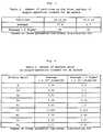
- FIG. 3is a table containing particle count data achieved by cleaning wafers with the method of the present invention.
- FIG. 4is a table containing metal atoms concentration data achieve by cleaning wafers with the method of the present invention.
- FIG. 5is a table containing concentration data for organic contaminants and ions achieved by cleaning wafers with the method of the present invention.
- the method of the present inventionprovides a means by which to readily and efficiently clean semiconductor wafers following final polishing.
- the surface of a contaminated semiconductor waferis sequentially treated with an oxidizing solution, treated with an alkaline cleaning solution in the presence of a sonic field, rinsed with deionized water, treated with an acidic solution, treated with an ozonated water rinse, and dried.
- the method of the present inventioncleans an incoming final polished semiconductor wafer in a single operation (i.e., following final polishing, a process or action is directed at the wafer which includes drying the wafer only once, thereby yielding a wafer substantially free from contaminants).
- contaminantsis to be understood as meaning, foreign metals, organic compounds, ions, and particulate having a diameter greater than about 0.2 ⁇ m adsorbed to the surface of a semiconductor wafer.
- the method of the present inventionfollowing final polishing, cleans a semiconductor wafer by oxidizing the wafer surface at the beginning of the operation and immediately prior to drying.
- the method of the present inventionreduces the manufacturing costs associated with the final cleaning of a semiconductor wafer, as well as reduces the amount of waste generated.
- the current standard for particulate matter on a Grade 1 waferis about 0.06 to about 0.1 particles exceeding 0.2 ⁇ m in diameter per cm 2 (about 40 to 100 particles on the front side of a 300 mm wafer).
- industry standards for cleanlinessare increasing. For example, according the 1997 National Technology Roadmap (published by the Semiconductor Industry Association as a guidebook for silicon wafer, electronic device and equipment manufacturers), the particle size limits will continue to decrease through the year 2012.
- the suggested 1999 valueis less than 60 particles exceeding 90 nm per 300 mm wafer, for 2006 the value is less than 27 particles exceeding 50 nm, and for 2012 the value is less than 22 particles exceeding 25 nm.
- the process of the present inventionalthough primarily concerned with particles exceeding about 0.2 ⁇ m (200 nm), is applicable to removing particles less than about 0.12 ⁇ m (120 nm), 0.09 ⁇ m (90 nm), and smaller.
- the current conventional detection limit for particlesis greater than about 0.09 ⁇ m.
- the process of the present inventionis well-suited for the cleaning of semiconductor wafers, preferably silicon wafers having a nominal diameter of 150 mm, 200 mm, 300 mm or even greater diameters.
- the starting wafersare preferably single-side polished or double-side polished wafers and are characterized as follows: wet or dry, the surface roughness is generally less than about 0.5 nm, and typically about 0.02 to about 0.2 nm; the total thickness variation is generally less than about 3 ⁇ m, and typically about 0.2 to about 2 ⁇ m; the concentration of contaminant particles exceeding about 0.2 ⁇ m in diameter adsorbed to the wafer surface is generally greater than about 15 particles/cm 2 , and typically greater than about 30 particles/cm 2 , 150 particles/cm 2 , or 3,000 particles/cm 2 ; the concentration of metals adsorbed to the wafer surface is generally greater than about 5 ⁇ 10 10 atoms/cm 2 , and typically greater than about 10 ⁇ 10 10 atoms/cm 2 , or
- the process of the present inventionbegins by treating a polished wafer with an oxidizing solution. It is preferred that this step be carried out before the alkaline and acidic cleaning steps of the present invention; the alkaline and acidic cleaning steps are not particularly well-suited for the removal of organic contaminants and may even be hampered by organic compounds on the wafer surface.
- the oxidizing solutionis capable of reducing the concentration of organic contaminants on the wafer surface.
- the oxidizing compoundis preferably capable of creating an oxide layer on the surface of the wafer of sufficient thickness to prevent direct silicon etching by subsequent alkaline washing solution steps (i.e., a layer of silicon oxide preferably remains on the wafer surface throughout the entire period the wafer is in contact with an alkaline solution).
- a silicon waferdoes not have an oxide layer on the surface which results in a hydrophobic surface. If an alkaline solution contacts the hydrophobic surface of the wafer, it tends to excessively etch the wafer surface causing roughening and pitting.
- silicon oxideis hydrophillic, its alkaline etch removal rate is about 1000 times slower than silicon, and as a result the etching process is readily controlled.
- surfactantsare adsorbed to the wafer surface. The surfactants make the surface of the wafer appear to be hydrophillic, however, they are quickly removed by alkaline solutions and the bare silicon wafer is excessively etched.
- an oxidized layeris preferably built up on the wafer prior to contact with the alkaline solution.
- the solutioncomprises an oxidizing compound with sufficient oxidizing ability, for example, ozone, peroxydisulfuric acid (generally created by heating sulfuric acid with oxidants such as hydrogen peroxide, nitric acid or ozone and commonly referred to as a Piranha process), permanganate, chromate, oxygen-halogen compounds such as perchlorate (hereinafter referred to as “oxy-halides”), and/or oxalic acid.
- the oxidizing solutionpreferably does not contain significant quantities of sulfur, organic compounds or metals which tend to increase the concentration of contaminants on the wafer surface.
- the oxidizing solutionpreferably comprises ozonated water. More preferably, the concentration of ozone is at least about 10 ppm. Because as the temperature of the water increases the saturation concentration decreases, the temperature of the ozonated water is preferably less than about 35° C., more preferably less than about 30° C., and still more preferably about 17 to about 25° C. At about 17 to about 25° C., the saturation concentration is about 30 to about 35 ppm, thus, preferably the concentration of ozone is maintained at least about 1 ⁇ 3 of saturation which corresponds to about 10 ppm. More preferably, the concentration of ozone is maintained at about 50% of saturation, still more preferably at least about 70%, still more preferably at least about 90%, and still more preferably at about 100%. Additionally, by using methods known in the art, supersaturation of ozone can be achieved and may be preferred.
- the amount of time the wafer is exposed to the ozonated wateris primarily a function of the amount of contamination and the concentration of dissolved ozone.
- the duration of the washis about 5 to about 30 minutes, and more preferably about 6 to about 8 minutes.
- the waferis treated with the ozone wash for as long as necessary to sufficiently clean the wafer.
- a wax mounted polishing operationresults in a relatively large amount of organic contaminants adhered to the wafer surface and can require, for example, up to about 30 minutes in the wash.
- a non-wax mounted polished wafermay only require about 6 to about 8 minutes in the wash.
- oxidation of the waferis accomplished in two or more steps. That is, the wafer is oxidized in sequential ozonated water baths preferably not exceeding about 8 to about 10 minutes, and more preferably about 6 to about 8 minutes.
- a multi-step washincreases throughput and prevents a bottleneck in the manufacturing process resulting from substantially different treatment durations for consecutive treatments. For example, a 6 minute treatment followed by a 20 minute treatment will result in a back-up of wafers in the manufacturing process. To further prevent back-ups, preferably the duration of each bath in the sequence is approximately equal.
- the multi-step washcan be in the form of multiple tanks, a single tank with sufficient length to accommodate multiple steps.
- an even more preferable method of preventing back-upsis using a smaller pitch, or space between wafers in the carrier, to increase the throughput (e.g., typically, 300 mm wafers are spaced about 10 mm apart, but to increase throughput the distance between the wafers, or pitch, can be reduced to about 5 mm).
- a 3 pitche.g., 5 mm instead of 10 mm
- twice as many waferscan be processed in the same amount of time without increasing the number of baths or the length of the baths.
- the wafersmay be treated with the ozonated water in a variety of manners (e.g., spraying, recirculated bath or overflow bath), it is preferred that the wafers be fully immersed in a recirculated and filtered bath (to reduce raw material costs and increase the cleaning efficiency by removing contaminants suspended in the bath). Due to the inefficiency of current methods of dissolving ozone into water, recirculation is an easy way to increase the ozone to saturation. Other methods of treatment, such as spraying, generally are less preferred because the dissolved ozone more readily comes out of solution.
- the oxide layeris preferably at least about 4 ⁇ thick, more preferably at least about 5 ⁇ , and still more preferably about 6 to about 10 ⁇ .
- the concentration of organic contaminants on the wafer after the washis preferably less than 5 ⁇ 10 15 carbon atoms/cm 2 , more preferably less than 1 ⁇ 10 15 carbon atoms/cm 2 , and still more preferably less than the detection limit for organic carbon (the detection limit of current equipment is about 1 ⁇ 10 10 carbon atoms/cm 2 , however, due to the high affinity between silicon and organic compounds, the practical detection limit for a silicon wafer is about 1 ⁇ 10 11 carbon atoms/cm 2 ).
- the wafer surfaceis treated with an alkaline solution in the presence of a sonic field which is capable of decreasing the amount of contaminants adsorbed to the wafer surface without directly etching non-oxidized wafer material, increasing the surface roughness of the wafer above about 0.01 nm, or detectably increasing the total thickness variation (the current detection limits for a change in thickness variation is about 0.01 ⁇ m).
- the alkaline cleaning solutioncomprises hydroxyl ions, hydrogen peroxide and deionized water.
- the source of the hydroxyl ionsis ammonium hydroxide and/or alkyl ammonium hydroxides such as tetra-methyl-ammonium hydroxide (TMAH) and tetra-ethyl-ammonium hydroxide.
- TMAHtetra-methyl-ammonium hydroxide
- the alkaline cleaning solutionconsists essentially of ammonium hydroxide, hydrogen peroxide and deionized water.
- the ratio of ammonium hydroxide, hydrogen peroxide and waterrange, respectively, from about 1:2:300 to about 1:10:20 by volume of commercially available reagent solutions, typically supplied as 28-30 wt % NH 4 OH in water and as 30-35 wt % H 2 O 2 in water.
- the ratios of ammonium hydroxide and hydrogen peroxideare expressed relative to water, but independent of each other. That is, in the solution described about, the ratio of NH 4 OH:H 2 O ranges from about 1:300 to about 1:20, the ratio of H 2 O 2 :H 2 O is about 1:150 to about 1:2, and both of these ratios (NH 4 OH:H 2 O and H 2 O 2 :H 2 O) are independent of each other.
- the concentration of ammonium hydroxideis less than about 2 moles per liter of water, and more preferably about 0.2 to about 0.5 moles per liter of water.
- the concentration of hydrogen peroxideis less than about 2 moles per liter of water, and more preferably about 0.3 to about 1.0 moles per liter of water.
- the ratio of ammonium hydroxide to hydrogen peroxideis such that silicon beneath the oxidized layer is not directly etched. More preferably, the ratio is maintained such that oxidation rate, in terms of oxide layer thickness, is at least about equal to the silicon oxide removal rate, and still more preferably the oxidation rate exceeds the silicon oxide removal rate.
- the volume ratio (using commercially available solutions) of NH 4 OH:H 2 O 2is about 1:1 to about 1:10, and more preferably about 1:2 to about 1:5.
- the alkaline solutionbe assisted by introducing energy in the form of sound waves into the alkaline bath.
- energy in the form of sound wavesis achieved by extremely high-frequency sonic energy while the wafer is submerged in the solution.
- the sonic energyis megasonic, having a frequency of about 0.8 to about 2 MHZ.
- megasonic sound wavesare generated by an array of piezoelectric transducers mounted to the bath wall.
- Particles ranging in size from several micrometers down to about 0.2 ⁇ m and smallerare efficiently removed with energy input of at least about 3 watts per 200 mm wafer.
- energy input levelsare maintained at about 3 to about 20 watts per 200 mm wafer.
- a tank designed to handle a loaded 25 wafer carrierwill preferably have an energy input level of about 75 to about 1500 watts. For wafers of different diameter, the energy input is adjusted based on watts per unit surface area to an equivalent energy level.
- the total power supplied to the megasonic transducerswill generally need to be greater than the total power being applied to the bath in which the wafers are situated due to operational constraints, heat losses and other inefficiencies associated with the various megasonic cleaning apparatus.
- the power supplied to a megasonic cleaning apparatus rated at 300 Wis typically limited to about 90% of its rated power—about 270 W.
- the power supplied to the bathwould be about 216 W and the megasonic power applied to twenty-five wafers in the bath would be about 9 W per wafer.
- the waferis preferably oriented in the etching bath in a manner which allows for acoustic streaming of the solution over the oxide layer (i.e., the front wafer surface is parallel to the direction in which the sound waves are transmitted through the solution).
- the temperature of the alkaline cleaning solutionis preferably at about 45 to about 75° C., more preferably about 55 to about 70° C., and still more preferably about 65° C. Also, it is preferred that the alkaline cleaning solution be recirculated and filtered (to reduce raw material costs and increase the cleaning efficiency by removing contaminants suspended in the bath).
- the waferis treated in the megasonic alkaline cleaning solution for at least as long as necessary to remove substantially all of the particulate contaminant.
- a wafer immersed in a single-step alkaline solutionis substantially free of particulate contaminants after about 20 to about 21 minutes.
- a shorter durationmay be adequate for a less contaminated wafer.
- the waferis immersed in two or more megasonic alkaline solution baths.
- the duration of each bathdoes not exceed about 8 to about 10 minutes each; and more preferably the duration of each bath is about 6 to about 8 minutes.
- the duration of each bath in the sequenceis preferably about equal. Even more preferably, the wafer is immersed in two alkaline solution baths for about 6 to 8 minutes each.
- concentration of particles exceeding 0.2 ⁇ m in diameter on the wafer surfaceis preferably less than about 0.06 to about 0.16 particles/cm 2 , and more preferably less than about 0.04 particles/cm 2 .
- the wafer surfaceis rinsed with deionized water.
- the deionized water rinseassists in the removal of contaminants on the wafer surface and removes residual amounts of previous treatment solutions (e.g., ammonium hydroxide or acid). If two or more megasonic alkaline solution baths are used, it is preferred to follow the first alkaline bath with a deionized water rinse in addition to a rinse following the final alkaline solution bath.
- the temperature of the deionized water rinseis about 17 to about 25° C.
- the waferis rinsed by a technique commonly referred to as a Quick Dump Rinse.
- the Quick Dump Rinse processcomprises placing a wafer in a tank filled with deionized water; as soon as the wafer is completely immersed, quick dump valves at the bottom of the tank are opened and the water rapidly flows from the tank; when the quick dump valves are opened the wafers are also sprayed with deionized water; when the tank is empty, the quick dump valves are closed and deionized water is pumped into the tank and the spray continues until the tank is full.
- the total dump timeis about 2 seconds and the fill time is less than about 1 minute.
- the fill timeis about 30 seconds or less.
- the fill rate for the tankis preferably at least about the volume of the tank per minute, and more preferably twice the volume of the tank per minute.
- a typical Quick Dump Rinse tankhas a volume of about 35 to about 50 liters, thus, the fill rate is preferably about 35 to 50 liters/minute, and more preferably about 70 to about 100 liters/minute.
- the deionized water rinsecomprises at least 2 Quick Dump Rinses, and more preferably 2 to 7 Quick Dump Rinses.
- the wafer surfaceis treated with an acidic solution.
- the primary purpose of the acid solutionis to further remove metal contamination without adding contaminants to the wafer surface.
- the acid solutionpreferably comprises acid and deionized water to preferably extract metals from the silicon oxide on the wafer surface without directly etching the oxide or underlying silicon.
- the acidis selected from the group consisting of nitric acid, citric acid, hydrochloric acid, and mixtures thereof. More preferably, the acid is hydrochloric acid.
- the concentration of acidis less than about 2 moles per liter of water, and more preferably about 0.01 to about 0.2 moles per liter of water.
- an oxidizing agentsuch as hydrogen peroxide and/or ozone may also be included in the acid solution.
- the concentration of hydrogen peroxideis less than about 2 moles per liter.
- the temperature of the acid solutionis about 17 to about 95° C., and more preferably about 25° C. to about 70° C.
- the waferis treated in the acid solution for at least as long as necessary to remove substantially all of the foreign metal contaminants.
- the amount of time required to adequately treat the wafer surface with the acid solutionis largely a function of metal contaminant concentration and solution temperature.
- the duration of the acid solution treatmentincreases with increasing contamination concentration and/or decreasing acid solution temperature.
- the duration of the acid washis about 4 to about 10 minutes, and more preferably about 5 to about 8 minutes.
- the wafersmay be treated with the acid solution in a variety of manners (e.g., spraying, recirculated bath, or ozone bath), it is preferred that the wafers be fully immersed in a recirculated and filtered bath (to reduce raw material costs and increase the cleaning efficiency by removing contaminants suspended in the bath).
- mannerse.g., spraying, recirculated bath, or ozone bath
- the wafersbe fully immersed in a recirculated and filtered bath (to reduce raw material costs and increase the cleaning efficiency by removing contaminants suspended in the bath).
- the waferAfter acid cleaning, the wafer preferably has less than about 1 ⁇ 10 10 metal atoms/cm 2 . More preferably, the concentration for each type of metal (e.g., iron, zinc and aluminum) is than about 1 ⁇ 10 10 atoms/cm 2 .
- the concentration for each type of metale.g., iron, zinc and aluminum
- the acid cleaningis followed by a deionized water rinse carried out in the same manner as the deionized rinse which follows the alkaline cleaning.
- the surface of the waferis treated with ozonated deionized water to remove residual acid solution, residual organic contaminants and ions such as ammonium which may have been adsorbed to the wafer during the preceding cleaning steps.
- the wafermay be treated with the ozonated water in a variety of manners (e.g., spraying, recirculated bath, overflow bath), however, the wafers are preferably immersed in an overflow bath which ensures the highest degree of wafer cleanliness.
- rinsing a carrier of wafers in an ozonated water overflow bathentails immersing the wafers in a tank containing ozonated water; while immersed, the to wafers are oxidized which removes contaminants; to increase the cleaning efficiency, fresh ozonated water is continually pumped into the tank; once the tank is full, ozonated water overflows the tank and contaminants suspended in the water are removed from the tank and cannot be redeposited on the wafers.
- the concentration of ozoneis at least about 1 ppm, more preferably about 1 to about 5 ppm, and still more preferably about 5 to about 15 ppm. Most preferably, the concentration of ozone is about saturation. However, due to the inefficiency of current methods of dissolving ozone into water, an ozone concentration approaching saturation is currently not attainable without recirculation. Thus, the concentration of ozone attainable in a conventional overflow bath is significantly less than saturation (e.g., less than about 50% saturation).
- the temperature of the ozonated wateris preferably less than about 35° C., more preferably less than about 30° C., and still more preferably about 17 to about 25° C.
- the amount of time the wafer is exposed to the ozonated wateris primarily a function of the amount of contamination and the concentration of dissolved ozone.
- the waferis rinsed in the ozonated water for at least as long as necessary to remove substantially all of the residual organic and ion contaminants—typically about 5 to about 8 minutes.
- the waferis dried by any acceptable method known in the art such as spin drying or IPA (drying with the aid of isopropyl alcohol), preferably by IPA drying.
- IPA dryingentails contacting a wet wafer with isopropyl alcohol, which is miscible in water. The alcohol decreases the surface tension of water which decreases the contact angle between the water and causes the water to roll off the wafer surface and the remaining alcohol evaporates.
- IPA dryingThere are three generally recognized methods of IPA drying: 1) Marangoni drying which entails pulling a wafer, submerged in water, through a water/isopropyl alcohol interface created by spraying alcohol across the top of the water; 2) Vapor Jet® by SCP Global Technology which dries the wafer by blowing nitrogen gas with about 1 to 2% isopropyl alcohol on the wafer surface; and 3) Vapor drying which entails placing a carrier full of wafers in a cloud of heated isopropyl alcohol vapor, alcohol condenses on the wafers, mixes with the water, and the water rolls of the wafer. Any of the foregoing IPA methods may be used, however, there are benefits and disadvantages associated with each.
- the waferis preferably dried using the IPA Vapor method.
- the temperature of the cloudis about 80 to about 85° C.
- the wafersare left in is the cloud until they reach the temperature of the cloud, typically, about 3 to about 10 minutes. However, if a low mass carrier is used the time can be reduced to about 2 to about 5 minutes.
- the wafer surfaceis substantially free of contaminants. More specifically, concentration of foreign metals on the wafer surface is less than about 1 ⁇ 10 10 atoms/cm 2 .
- concentration of particulate exceeding 0.02 ⁇ m in diameteris less than about 0.06 to about 0.16 particles/cm 2 , and preferably less than about 0.04 particles/cm 2 .
- concentration of particulate exceeding 0.12 ⁇ m in diameteris less than about 0.13 particles/cm 2 , and preferably less than 0.10 particles/cm 2 .
- the concentration of organic contaminantsis less than about 1 ⁇ 10 14 carbon atoms/cm 2 , preferably less than about 0.1 to 0.5 ⁇ 10 14 carbon atoms/cm 2 , and more preferably less than about 1 ⁇ 10 11 carbon atoms/cm.
- the cleaning method of the present inventioneffectively removes all other ions such as ammonia so that degradation haze preferably does not occur.
- the surface roughnessis about 0.02 to 0.5 nm and the total thickness variation is about 0.02 to about 2 ⁇ m.
- incoming 300 mm waferswere sequentially immersed in a recirculated ozone water bath having an ozone concentration of 25 ppm for 9 min; immersed in a recirculated megasonic alkaline solution bath at 65° C., 500 W energy input, for 8 min. 40 sec.; rinsed with 6 Quick Dump Rinses; immersed in a recirculated megasonic alkaline solution bath at 65° C., 500 W energy input, for 8 min.; rinsed with 6 Quick Dump Rinses; immersed in a recirculated acid solution at 70° C. for 7 min.
- the average level of surface ionsis sufficiently low that no degradation haze is observed after a four day rapid haze test which entails exposing a wafer to a closed atmosphere in the presence of 10 mL of water sequentially for 24 hours at about 50° C., 24 hours at about ⁇ 5° C., 48 hours at room temperature (about 25° C.), and inspecting the surface of the wafer for a change in the number of particles exceeding 0.12 ⁇ m.
Landscapes
- Engineering & Computer Science (AREA)
- Physics & Mathematics (AREA)
- Condensed Matter Physics & Semiconductors (AREA)
- General Physics & Mathematics (AREA)
- Manufacturing & Machinery (AREA)
- Computer Hardware Design (AREA)
- Microelectronics & Electronic Packaging (AREA)
- Power Engineering (AREA)
- Cleaning Or Drying Semiconductors (AREA)
- Mechanical Treatment Of Semiconductor (AREA)
Abstract
Description
Claims (54)
Priority Applications (3)
| Application Number | Priority Date | Filing Date | Title |
|---|---|---|---|
| US09/606,728US6230720B1 (en) | 1999-08-16 | 2000-06-29 | Single-operation method of cleaning semiconductors after final polishing |
| PCT/US2000/021601WO2001013418A1 (en) | 1999-08-16 | 2000-08-08 | A single-operation method of cleaning semiconductors after final polishing |
| TW089116534ATW473852B (en) | 1999-08-16 | 2000-10-12 | A single-operation method of cleaning semiconductors after final polishing |
Applications Claiming Priority (3)
| Application Number | Priority Date | Filing Date | Title |
|---|---|---|---|
| US14912399P | 1999-08-16 | 1999-08-16 | |
| US14921299P | 1999-08-17 | 1999-08-17 | |
| US09/606,728US6230720B1 (en) | 1999-08-16 | 2000-06-29 | Single-operation method of cleaning semiconductors after final polishing |
Publications (1)
| Publication Number | Publication Date |
|---|---|
| US6230720B1true US6230720B1 (en) | 2001-05-15 |
Family
ID=27386793
Family Applications (1)
| Application Number | Title | Priority Date | Filing Date |
|---|---|---|---|
| US09/606,728Expired - Fee RelatedUS6230720B1 (en) | 1999-08-16 | 2000-06-29 | Single-operation method of cleaning semiconductors after final polishing |
Country Status (3)
| Country | Link |
|---|---|
| US (1) | US6230720B1 (en) |
| TW (1) | TW473852B (en) |
| WO (1) | WO2001013418A1 (en) |
Cited By (42)
| Publication number | Priority date | Publication date | Assignee | Title |
|---|---|---|---|---|
| US6492275B2 (en)* | 2000-01-21 | 2002-12-10 | Advanced Micro Devices, Inc. | Control of transistor performance through adjustment of spacer oxide profile with a wet etch |
| US6503333B2 (en)* | 2000-11-30 | 2003-01-07 | Taiwan Semiconductor Manufacturing Company, Ltd | Method for cleaning semiconductor wafers with ozone-containing solvent |
| US20030034048A1 (en)* | 2001-08-17 | 2003-02-20 | Nec Corporation | Back-surface cleaning method for cleaning the back surface of a silicon wafer |
| US6530381B1 (en)* | 1999-11-04 | 2003-03-11 | WACKER SILTRONIC GESELLSCHAFT FüR HALBLEITERMATERIALIEN AG | Process for the wet-chemical surface treatment of a semiconductor wafer |
| US6558478B1 (en)* | 1999-10-06 | 2003-05-06 | Ebara Corporation | Method of and apparatus for cleaning substrate |
| US6638365B2 (en)* | 2001-10-09 | 2003-10-28 | Chartered Semiconductor Manufacturing Ltd. | Method for obtaining clean silicon surfaces for semiconductor manufacturing |
| WO2003090263A1 (en)* | 2002-04-17 | 2003-10-30 | Lam Research Corporation | Silicon parts for plasma reaction chambers |
| US20040029494A1 (en)* | 2002-08-09 | 2004-02-12 | Souvik Banerjee | Post-CMP cleaning of semiconductor wafer surfaces using a combination of aqueous and CO2 based cryogenic cleaning techniques |
| US6696361B2 (en)* | 2001-04-24 | 2004-02-24 | United Microelectronics Corp. | Post-CMP removal of surface contaminants from silicon wafer |
| US6716290B1 (en)* | 2002-12-04 | 2004-04-06 | The United States Of America As Represented By The Secretary Of The Navy | Method for removing soldering flux residue from a substrate |
| US20040084059A1 (en)* | 2002-10-31 | 2004-05-06 | Texas Instruments Incorporated | Modified clean chemistry and megasonic nozzle for removing backside CMP slurries |
| US20040188387A1 (en)* | 2003-03-25 | 2004-09-30 | Brask Justin K. | Removing silicon nano-crystals |
| US20040231705A1 (en)* | 2003-05-21 | 2004-11-25 | Nihon Ceratec Co., Ltd. | Cleaning method of ceramic member |
| US20040238119A1 (en)* | 2003-05-26 | 2004-12-02 | Ching-Yu Chang | [apparatus and method for etching silicon nitride thin film ] |
| US6867148B2 (en)* | 2001-05-16 | 2005-03-15 | Micron Technology, Inc. | Removal of organic material in integrated circuit fabrication using ozonated organic acid solutions |
| US20060003134A1 (en)* | 2004-07-01 | 2006-01-05 | Sumitomo Electric Industries, Ltd. | AlxGayIn1-x-yN substrate, cleaning method of AlxGayIn1-x-yN substrate, AIN substrate, and cleaning method of AIN substrate |
| US20060070979A1 (en)* | 2004-09-17 | 2006-04-06 | Christenson Kurt K | Using ozone to process wafer like objects |
| US20070066071A1 (en)* | 2005-09-16 | 2007-03-22 | Taiwan Semiconductor Manufacturing Company, Ltd. | Novel organic remover for advanced reticle contamination cleaning |
| US20070072423A1 (en)* | 2005-09-29 | 2007-03-29 | Siltronic Ag | Unpolished semiconductor wafer and method for producing an unpolished semiconductor wafer |
| US20070197037A1 (en)* | 2006-02-21 | 2007-08-23 | Matt Yeh | Surface preparation for gate oxide formation that avoids chemical oxide formation |
| US20070240737A1 (en)* | 2002-09-30 | 2007-10-18 | Lam Research Corporation | Post etch wafer surface cleaning with liquid meniscus |
| US20080057706A1 (en)* | 2006-08-30 | 2008-03-06 | Gyu Hyun Kim | Method for forming cyclinder type storage node for preventing creation of watermarks |
| US20080227271A1 (en)* | 2007-03-14 | 2008-09-18 | Sumco Corporation | Method of manufacturing bonded wafer |
| US20090056744A1 (en)* | 2007-08-29 | 2009-03-05 | Micron Technology, Inc. | Wafer cleaning compositions and methods |
| US20090095321A1 (en)* | 2007-10-10 | 2009-04-16 | Siltron Inc. | Method for cleaning silicon wafer |
| US20090126760A1 (en)* | 2005-01-12 | 2009-05-21 | Boc, Inc. | System for cleaning a surface using crogenic aerosol and fluid reactant |
| US20090203212A1 (en)* | 2005-11-30 | 2009-08-13 | Shin-Etsu Handotai Co Ltd. | Surface Grinding Method and Manufacturing Method for Semiconductor Wafer |
| US20110045673A1 (en)* | 2008-03-14 | 2011-02-24 | Rena Gmbh | Method for manufacturing a silicon surface with pyramidal texture |
| US20110053349A1 (en)* | 2009-08-31 | 2011-03-03 | Semiconductor Manufacturing International (Shanghai) Corporation | Application of millisecond heating source for surface treatment |
| US20110065281A1 (en)* | 2009-09-11 | 2011-03-17 | Semiconductor Manufacturing International (Shanghai) Corporation | Method of rapid thermal treatment using high energy electromagnetic radiation of a semiconductor substrate for formation of epitaxial materials |
| US20110067734A1 (en)* | 2009-09-24 | 2011-03-24 | Kabushiki Kaisha Toshiba | Apparatus and method for cleaning semiconductor substrate |
| US20110111548A1 (en)* | 2009-10-05 | 2011-05-12 | Ismail Kashkoush | Method of manufacturing a solar cell using a pre-cleaning step that contributes to homogeneous texture morphology |
| US20110306210A1 (en)* | 2007-02-16 | 2011-12-15 | Ismail Kashkoush | Method for cleaning substrates utilizing surface passivation and/or oxide layer growth to protect from pitting |
| US20130068248A1 (en)* | 2011-09-15 | 2013-03-21 | Taiwan Semiconductor Manufacturing Company, Ltd., ("Tsmc") | Semiconductor device cleaning method |
| US20130291925A1 (en)* | 2011-01-26 | 2013-11-07 | Shigeru Okuuchi | Solar cell wafer and method of producing the same |
| US20140318578A1 (en)* | 2013-04-30 | 2014-10-30 | Corning Incorporated | Method of cleaning glass substrates |
| US10077206B2 (en)* | 2015-06-10 | 2018-09-18 | Corning Incorporated | Methods of etching glass substrates and glass substrates |
| CN109801836A (en)* | 2013-02-15 | 2019-05-24 | 弗赖贝格化合物原料有限公司 | It is used to prepare method, the gallium arsenide substrate and application thereof of gallium arsenide substrate |
| CN111816548A (en)* | 2020-05-11 | 2020-10-23 | 中环领先半导体材料有限公司 | Process for improving edge roughness of large-diameter semiconductor silicon wafer by edge polishing |
| CN114678259A (en)* | 2022-05-30 | 2022-06-28 | 杭州乾晶半导体有限公司 | Method for cleaning polished silicon carbide wafer and corresponding cleaning agent |
| CN116454174A (en)* | 2023-06-16 | 2023-07-18 | 福建金石能源有限公司 | Back polishing method of back contact battery |
| CN120527222A (en)* | 2025-07-24 | 2025-08-22 | 南通咸昌新材料科技有限公司 | Surface cleaning method for (111) crystal orientation indium antimonide wafer |
Families Citing this family (5)
| Publication number | Priority date | Publication date | Assignee | Title |
|---|---|---|---|---|
| JP4613744B2 (en)* | 2005-08-10 | 2011-01-19 | 株式会社Sumco | Cleaning method of silicon wafer |
| DE102008056455B3 (en)* | 2008-11-07 | 2010-04-29 | Centrotherm Photovoltaics Technology Gmbh | Oxidation and cleaning process for silicon wafers |
| DE102013213839A1 (en)* | 2013-07-15 | 2015-01-15 | Siltronic Ag | Process for producing a highly doped semiconductor wafer |
| EP3139416B1 (en) | 2015-09-07 | 2020-10-28 | IMEC vzw | Texturing monocrystalline silicon substrates |
| CN111376169A (en)* | 2018-12-28 | 2020-07-07 | 安集微电子科技(上海)股份有限公司 | Method for cleaning polished wafer |
Citations (17)
| Publication number | Priority date | Publication date | Assignee | Title |
|---|---|---|---|---|
| US4050954A (en) | 1976-03-25 | 1977-09-27 | International Business Machines Corporation | Surface treatment of semiconductor substrates |
| EP0701275A2 (en) | 1994-08-26 | 1996-03-13 | MEMC Electronic Materials, Inc. | Pre-thermal treatment cleaning process |
| EP0718873A2 (en) | 1994-12-21 | 1996-06-26 | MEMC Electronic Materials, Inc. | Cleaning process for hydrophobic silicon wafers |
| US5626159A (en) | 1995-04-19 | 1997-05-06 | Memc Electronic Materials, Inc. | Apparatus for cleaning semiconductor wafers |
| US5635053A (en) | 1994-10-28 | 1997-06-03 | Nec Corporation | Method and apparatus for cleaning electronic parts |
| US5637151A (en) | 1994-06-27 | 1997-06-10 | Siemens Components, Inc. | Method for reducing metal contamination of silicon wafers during semiconductor manufacturing |
| US5656097A (en) | 1993-10-20 | 1997-08-12 | Verteq, Inc. | Semiconductor wafer cleaning system |
| US5679171A (en) | 1995-03-27 | 1997-10-21 | Sony Corporation | Method of cleaning substrate |
| US5695572A (en) | 1994-08-25 | 1997-12-09 | Wacker Siltronic Gesellschaft Fur Halbleitermaterialien Aktiengesellschaft | Cleaning agent and method for cleaning semiconductor wafers |
| EP0844650A2 (en) | 1996-11-15 | 1998-05-27 | MEMC Electronic Materials, Inc. | Method of etching SiO2 and process of cleaning silicon wafers using dilute chemical etchants and a megasonic field |
| US5830280A (en)* | 1996-03-15 | 1998-11-03 | Tokyo Electron Limited | Washing liquid for post-polishing and polishing-cleaning method in semiconductor process |
| US5837662A (en) | 1997-12-12 | 1998-11-17 | Memc Electronic Materials, Inc. | Post-lapping cleaning process for silicon wafers |
| US5932022A (en)* | 1998-04-21 | 1999-08-03 | Harris Corporation | SC-2 based pre-thermal treatment wafer cleaning process |
| US5938857A (en)* | 1997-08-08 | 1999-08-17 | Nec Corporation | Method for rinsing and drying a substrate |
| US6099662A (en)* | 1999-02-11 | 2000-08-08 | Taiwan Semiconductor Manufacturing Company | Process for cleaning a semiconductor substrate after chemical-mechanical polishing |
| US6146467A (en)* | 1998-08-28 | 2000-11-14 | Mitsubishi Materials Silicon Corporation | Treatment method for semiconductor substrates |
| US6165279A (en)* | 1998-10-14 | 2000-12-26 | United Silicon Incorporated | Method for cleaning a semiconductor wafer |
Family Cites Families (1)
| Publication number | Priority date | Publication date | Assignee | Title |
|---|---|---|---|---|
| JPH11233476A (en)* | 1997-12-01 | 1999-08-27 | Mitsubishi Electric Corp | Semiconductor substrate processing method |
- 2000
- 2000-06-29USUS09/606,728patent/US6230720B1/ennot_activeExpired - Fee Related
- 2000-08-08WOPCT/US2000/021601patent/WO2001013418A1/enactiveApplication Filing
- 2000-10-12TWTW089116534Apatent/TW473852B/ennot_activeIP Right Cessation
Patent Citations (20)
| Publication number | Priority date | Publication date | Assignee | Title |
|---|---|---|---|---|
| US4050954A (en) | 1976-03-25 | 1977-09-27 | International Business Machines Corporation | Surface treatment of semiconductor substrates |
| US5656097A (en) | 1993-10-20 | 1997-08-12 | Verteq, Inc. | Semiconductor wafer cleaning system |
| US5637151A (en) | 1994-06-27 | 1997-06-10 | Siemens Components, Inc. | Method for reducing metal contamination of silicon wafers during semiconductor manufacturing |
| US5695572A (en) | 1994-08-25 | 1997-12-09 | Wacker Siltronic Gesellschaft Fur Halbleitermaterialien Aktiengesellschaft | Cleaning agent and method for cleaning semiconductor wafers |
| EP0701275A2 (en) | 1994-08-26 | 1996-03-13 | MEMC Electronic Materials, Inc. | Pre-thermal treatment cleaning process |
| US5516730A (en)* | 1994-08-26 | 1996-05-14 | Memc Electronic Materials, Inc. | Pre-thermal treatment cleaning process of wafers |
| US5712198A (en) | 1994-08-26 | 1998-01-27 | Memc Electronic Materials, Inc. | Pre-thermal treatment cleaning process |
| US5635053A (en) | 1994-10-28 | 1997-06-03 | Nec Corporation | Method and apparatus for cleaning electronic parts |
| EP0718873A2 (en) | 1994-12-21 | 1996-06-26 | MEMC Electronic Materials, Inc. | Cleaning process for hydrophobic silicon wafers |
| US5679171A (en) | 1995-03-27 | 1997-10-21 | Sony Corporation | Method of cleaning substrate |
| US5626159A (en) | 1995-04-19 | 1997-05-06 | Memc Electronic Materials, Inc. | Apparatus for cleaning semiconductor wafers |
| US5830280A (en)* | 1996-03-15 | 1998-11-03 | Tokyo Electron Limited | Washing liquid for post-polishing and polishing-cleaning method in semiconductor process |
| EP0844650A2 (en) | 1996-11-15 | 1998-05-27 | MEMC Electronic Materials, Inc. | Method of etching SiO2 and process of cleaning silicon wafers using dilute chemical etchants and a megasonic field |
| US5919311A (en) | 1996-11-15 | 1999-07-06 | Memc Electronic Materials, Inc. | Control of SiO2 etch rate using dilute chemical etchants in the presence of a megasonic field |
| US5938857A (en)* | 1997-08-08 | 1999-08-17 | Nec Corporation | Method for rinsing and drying a substrate |
| US5837662A (en) | 1997-12-12 | 1998-11-17 | Memc Electronic Materials, Inc. | Post-lapping cleaning process for silicon wafers |
| US5932022A (en)* | 1998-04-21 | 1999-08-03 | Harris Corporation | SC-2 based pre-thermal treatment wafer cleaning process |
| US6146467A (en)* | 1998-08-28 | 2000-11-14 | Mitsubishi Materials Silicon Corporation | Treatment method for semiconductor substrates |
| US6165279A (en)* | 1998-10-14 | 2000-12-26 | United Silicon Incorporated | Method for cleaning a semiconductor wafer |
| US6099662A (en)* | 1999-02-11 | 2000-08-08 | Taiwan Semiconductor Manufacturing Company | Process for cleaning a semiconductor substrate after chemical-mechanical polishing |
Non-Patent Citations (1)
| Title |
|---|
| PCT International Search Report for PCT/US00/21601 dated Nov. 29, 2000. |
Cited By (81)
| Publication number | Priority date | Publication date | Assignee | Title |
|---|---|---|---|---|
| US6745784B2 (en) | 1999-10-06 | 2004-06-08 | Ebara Corporation | Method of and apparatus for cleaning substrate |
| US6558478B1 (en)* | 1999-10-06 | 2003-05-06 | Ebara Corporation | Method of and apparatus for cleaning substrate |
| US20030168089A1 (en)* | 1999-10-06 | 2003-09-11 | Ichiro Katakabe | Method of and apparatus for cleaning substrate |
| US6530381B1 (en)* | 1999-11-04 | 2003-03-11 | WACKER SILTRONIC GESELLSCHAFT FüR HALBLEITERMATERIALIEN AG | Process for the wet-chemical surface treatment of a semiconductor wafer |
| US6492275B2 (en)* | 2000-01-21 | 2002-12-10 | Advanced Micro Devices, Inc. | Control of transistor performance through adjustment of spacer oxide profile with a wet etch |
| US6503333B2 (en)* | 2000-11-30 | 2003-01-07 | Taiwan Semiconductor Manufacturing Company, Ltd | Method for cleaning semiconductor wafers with ozone-containing solvent |
| US6696361B2 (en)* | 2001-04-24 | 2004-02-24 | United Microelectronics Corp. | Post-CMP removal of surface contaminants from silicon wafer |
| US6867148B2 (en)* | 2001-05-16 | 2005-03-15 | Micron Technology, Inc. | Removal of organic material in integrated circuit fabrication using ozonated organic acid solutions |
| US20030034048A1 (en)* | 2001-08-17 | 2003-02-20 | Nec Corporation | Back-surface cleaning method for cleaning the back surface of a silicon wafer |
| US6638365B2 (en)* | 2001-10-09 | 2003-10-28 | Chartered Semiconductor Manufacturing Ltd. | Method for obtaining clean silicon surfaces for semiconductor manufacturing |
| US20040161943A1 (en)* | 2002-04-17 | 2004-08-19 | Daxing Ren | Silicon parts having reduced metallic impurity concentration for plasma reaction chambers |
| US7517803B2 (en) | 2002-04-17 | 2009-04-14 | Lam Research Corporation | Silicon parts having reduced metallic impurity concentration for plasma reaction chambers |
| WO2003090263A1 (en)* | 2002-04-17 | 2003-10-30 | Lam Research Corporation | Silicon parts for plasma reaction chambers |
| US6846726B2 (en) | 2002-04-17 | 2005-01-25 | Lam Research Corporation | Silicon parts having reduced metallic impurity concentration for plasma reaction chambers |
| US20050045593A1 (en)* | 2002-04-17 | 2005-03-03 | Lam Research Corporation | Silicon parts having reduced metallic impurity concentration for plasma reaction chambers |
| CN100377836C (en)* | 2002-08-09 | 2008-04-02 | 波克股份有限公司 | Post-CMP cleaning of semiconductor wafer surfaces using a combination of aqueous and cryogenic cleaning techniques |
| US20040029494A1 (en)* | 2002-08-09 | 2004-02-12 | Souvik Banerjee | Post-CMP cleaning of semiconductor wafer surfaces using a combination of aqueous and CO2 based cryogenic cleaning techniques |
| US20070240737A1 (en)* | 2002-09-30 | 2007-10-18 | Lam Research Corporation | Post etch wafer surface cleaning with liquid meniscus |
| US7597765B2 (en) | 2002-09-30 | 2009-10-06 | Lam Research Corporation | Post etch wafer surface cleaning with liquid meniscus |
| US7067015B2 (en)* | 2002-10-31 | 2006-06-27 | Texas Instruments Incorporated | Modified clean chemistry and megasonic nozzle for removing backside CMP slurries |
| US20040084059A1 (en)* | 2002-10-31 | 2004-05-06 | Texas Instruments Incorporated | Modified clean chemistry and megasonic nozzle for removing backside CMP slurries |
| US6716290B1 (en)* | 2002-12-04 | 2004-04-06 | The United States Of America As Represented By The Secretary Of The Navy | Method for removing soldering flux residue from a substrate |
| US20070105324A1 (en)* | 2003-03-25 | 2007-05-10 | Brask Justin K | Removing silicon nano-crystals |
| US20050181622A1 (en)* | 2003-03-25 | 2005-08-18 | Brask Justin K. | Removing silicon nano-crystals |
| US20040188387A1 (en)* | 2003-03-25 | 2004-09-30 | Brask Justin K. | Removing silicon nano-crystals |
| US20040231705A1 (en)* | 2003-05-21 | 2004-11-25 | Nihon Ceratec Co., Ltd. | Cleaning method of ceramic member |
| US6863740B2 (en)* | 2003-05-21 | 2005-03-08 | Nihon Ceratec Co., Ltd. | Cleaning method of ceramic member |
| US20040238119A1 (en)* | 2003-05-26 | 2004-12-02 | Ching-Yu Chang | [apparatus and method for etching silicon nitride thin film ] |
| TWI408263B (en)* | 2004-07-01 | 2013-09-11 | Sumitomo Electric Industries | Alxgayin1-x-yn substrate, cleaning method of alxgayin1-x-yn substrate, aln substrate, and cleaning method of aln substrate |
| US7387989B2 (en)* | 2004-07-01 | 2008-06-17 | Sumitomo Electric Industries, Ltd. | AlxGayInl−x−yN substrate, cleaning method of AlxGayInl−x−yN substrate, AlN substrate, and cleaning method of AlN substrate |
| US20060003134A1 (en)* | 2004-07-01 | 2006-01-05 | Sumitomo Electric Industries, Ltd. | AlxGayIn1-x-yN substrate, cleaning method of AlxGayIn1-x-yN substrate, AIN substrate, and cleaning method of AIN substrate |
| US20080299375A1 (en)* | 2004-07-01 | 2008-12-04 | Sumitomo Electric Industries, Ltd. | ALxGayIn1-x-yN substrate, cleaning method of AIxGayIn1-x-yN substrate, AIN substrate, and cleaning method of AIN substrate |
| US20060070979A1 (en)* | 2004-09-17 | 2006-04-06 | Christenson Kurt K | Using ozone to process wafer like objects |
| US20090126760A1 (en)* | 2005-01-12 | 2009-05-21 | Boc, Inc. | System for cleaning a surface using crogenic aerosol and fluid reactant |
| US20070066071A1 (en)* | 2005-09-16 | 2007-03-22 | Taiwan Semiconductor Manufacturing Company, Ltd. | Novel organic remover for advanced reticle contamination cleaning |
| US20070072423A1 (en)* | 2005-09-29 | 2007-03-29 | Siltronic Ag | Unpolished semiconductor wafer and method for producing an unpolished semiconductor wafer |
| US7754009B2 (en)* | 2005-09-29 | 2010-07-13 | Siltronic Ag | Unpolished semiconductor wafer and method for producing an unpolished semiconductor wafer |
| US20100237474A1 (en)* | 2005-09-29 | 2010-09-23 | Siltronic Ag | Unpolished Semiconductor Wafer and Method For Producing An Unpolished Semiconductor Wafer |
| US20090203212A1 (en)* | 2005-11-30 | 2009-08-13 | Shin-Etsu Handotai Co Ltd. | Surface Grinding Method and Manufacturing Method for Semiconductor Wafer |
| US20070197037A1 (en)* | 2006-02-21 | 2007-08-23 | Matt Yeh | Surface preparation for gate oxide formation that avoids chemical oxide formation |
| US7727900B2 (en)* | 2006-02-21 | 2010-06-01 | Taiwan Semiconductor Manufacturing Co., Ltd. | Surface preparation for gate oxide formation that avoids chemical oxide formation |
| WO2008002669A3 (en)* | 2006-06-28 | 2008-05-02 | Lam Res Corp | Post etch wafer surface cleaning with liquid meniscus |
| CN101479831B (en)* | 2006-06-28 | 2012-05-16 | 朗姆研究公司 | Post-etch wafer surface cleaning using a meniscus |
| US20080057706A1 (en)* | 2006-08-30 | 2008-03-06 | Gyu Hyun Kim | Method for forming cyclinder type storage node for preventing creation of watermarks |
| US20110306210A1 (en)* | 2007-02-16 | 2011-12-15 | Ismail Kashkoush | Method for cleaning substrates utilizing surface passivation and/or oxide layer growth to protect from pitting |
| US8741066B2 (en)* | 2007-02-16 | 2014-06-03 | Akrion Systems, Llc | Method for cleaning substrates utilizing surface passivation and/or oxide layer growth to protect from pitting |
| EP1970949B1 (en)* | 2007-03-14 | 2017-03-22 | SUMCO Corporation | Method of manufacturing bonded wafer |
| US20080227271A1 (en)* | 2007-03-14 | 2008-09-18 | Sumco Corporation | Method of manufacturing bonded wafer |
| US8802540B2 (en) | 2007-03-14 | 2014-08-12 | Sumco Corporation | Method of manufacturing bonded wafer |
| US20090056744A1 (en)* | 2007-08-29 | 2009-03-05 | Micron Technology, Inc. | Wafer cleaning compositions and methods |
| US20090095321A1 (en)* | 2007-10-10 | 2009-04-16 | Siltron Inc. | Method for cleaning silicon wafer |
| US20110045673A1 (en)* | 2008-03-14 | 2011-02-24 | Rena Gmbh | Method for manufacturing a silicon surface with pyramidal texture |
| US20110053349A1 (en)* | 2009-08-31 | 2011-03-03 | Semiconductor Manufacturing International (Shanghai) Corporation | Application of millisecond heating source for surface treatment |
| US8148272B2 (en)* | 2009-08-31 | 2012-04-03 | Semiconductor Manufacturing International (Shanghai) Corporation | Application of millisecond heating source for surface treatment |
| US8309472B2 (en)* | 2009-09-11 | 2012-11-13 | Semiconductor Manufacturing International (Shanghai) Corporation | Method of rapid thermal treatment using high energy electromagnetic radiation of a semiconductor substrate for formation of epitaxial materials |
| US20110065281A1 (en)* | 2009-09-11 | 2011-03-17 | Semiconductor Manufacturing International (Shanghai) Corporation | Method of rapid thermal treatment using high energy electromagnetic radiation of a semiconductor substrate for formation of epitaxial materials |
| US8758521B2 (en)* | 2009-09-24 | 2014-06-24 | Kabushiki Kaisha Toshiba | Apparatus and method for cleaning semiconductor substrate |
| US20110067734A1 (en)* | 2009-09-24 | 2011-03-24 | Kabushiki Kaisha Toshiba | Apparatus and method for cleaning semiconductor substrate |
| US9761466B2 (en) | 2009-09-24 | 2017-09-12 | Toshiba Memory Corporation | Apparatus and method for cleaning semiconductor substrate |
| US8084280B2 (en)* | 2009-10-05 | 2011-12-27 | Akrion Systems, Llc | Method of manufacturing a solar cell using a pre-cleaning step that contributes to homogeneous texture morphology |
| US20110111548A1 (en)* | 2009-10-05 | 2011-05-12 | Ismail Kashkoush | Method of manufacturing a solar cell using a pre-cleaning step that contributes to homogeneous texture morphology |
| US20130291925A1 (en)* | 2011-01-26 | 2013-11-07 | Shigeru Okuuchi | Solar cell wafer and method of producing the same |
| US9276153B2 (en)* | 2011-01-26 | 2016-03-01 | Sumco Corporation | Solar cell wafer and method of producing the same |
| US20130068248A1 (en)* | 2011-09-15 | 2013-03-21 | Taiwan Semiconductor Manufacturing Company, Ltd., ("Tsmc") | Semiconductor device cleaning method |
| CN109801836A (en)* | 2013-02-15 | 2019-05-24 | 弗赖贝格化合物原料有限公司 | It is used to prepare method, the gallium arsenide substrate and application thereof of gallium arsenide substrate |
| US12205815B2 (en) | 2013-02-15 | 2025-01-21 | Freiberger Compound Materials Gmbh | Gallium arsenide substrate comprising a surface oxide layer with improved surface homogeneity |
| US10460924B2 (en)* | 2013-02-15 | 2019-10-29 | Freiberger Compound Materials Gmbh | Process for producing a gallium arsenide substrate which includes marangoni drying |
| US11170989B2 (en)* | 2013-02-15 | 2021-11-09 | Freiberger Compound Materials Gmbh | Gallium arsenide substrate comprising a surface oxide layer with improved surface homogeneity |
| US9561982B2 (en)* | 2013-04-30 | 2017-02-07 | Corning Incorporated | Method of cleaning glass substrates |
| CN105340057A (en)* | 2013-04-30 | 2016-02-17 | 康宁股份有限公司 | Method of cleaning glass substrates |
| WO2014179251A1 (en)* | 2013-04-30 | 2014-11-06 | Corning Incorporated | Method of cleaning glass substrates |
| CN105340057B (en)* | 2013-04-30 | 2018-01-16 | 康宁股份有限公司 | Methods of Cleaning Glass Substrates |
| US20140318578A1 (en)* | 2013-04-30 | 2014-10-30 | Corning Incorporated | Method of cleaning glass substrates |
| JP2016523792A (en)* | 2013-04-30 | 2016-08-12 | コーニング インコーポレイテッド | Glass substrate cleaning method |
| US10077206B2 (en)* | 2015-06-10 | 2018-09-18 | Corning Incorporated | Methods of etching glass substrates and glass substrates |
| CN111816548A (en)* | 2020-05-11 | 2020-10-23 | 中环领先半导体材料有限公司 | Process for improving edge roughness of large-diameter semiconductor silicon wafer by edge polishing |
| CN114678259B (en)* | 2022-05-30 | 2023-11-17 | 杭州乾晶半导体有限公司 | A cleaning method for polished silicon carbide wafers and corresponding cleaning agents |
| CN114678259A (en)* | 2022-05-30 | 2022-06-28 | 杭州乾晶半导体有限公司 | Method for cleaning polished silicon carbide wafer and corresponding cleaning agent |
| CN116454174A (en)* | 2023-06-16 | 2023-07-18 | 福建金石能源有限公司 | Back polishing method of back contact battery |
| CN116454174B (en)* | 2023-06-16 | 2023-09-08 | 福建金石能源有限公司 | A kind of back polishing method for back contact battery |
| CN120527222A (en)* | 2025-07-24 | 2025-08-22 | 南通咸昌新材料科技有限公司 | Surface cleaning method for (111) crystal orientation indium antimonide wafer |
Also Published As
| Publication number | Publication date |
|---|---|
| WO2001013418A1 (en) | 2001-02-22 |
| TW473852B (en) | 2002-01-21 |
Similar Documents
| Publication | Publication Date | Title |
|---|---|---|
| US6230720B1 (en) | Single-operation method of cleaning semiconductors after final polishing | |
| JP3154814B2 (en) | Semiconductor wafer cleaning method and cleaning apparatus | |
| JP2760418B2 (en) | Semiconductor wafer cleaning solution and method for cleaning semiconductor wafer using the same | |
| KR100220926B1 (en) | Method for Cleaning Hydrophobic Silicon Wafers | |
| US20080156349A1 (en) | Method for cleaning silicon wafer | |
| JPH08264500A (en) | Cleaning of substrate | |
| WO1999031724A1 (en) | Post-lapping cleaning process for silicon wafers | |
| JP2007165935A (en) | How to remove metal in scrubbers | |
| JP2009543344A (en) | Post-etch wafer surface cleaning with liquid meniscus | |
| JP2005244179A (en) | Wet cleaning method of material surface and manufacturing process of electronic, optical or optoelectronic device using the same | |
| CN113675073A (en) | Wafer cleaning method | |
| CN112928017A (en) | Cleaning method for effectively removing metal on surface of silicon wafer | |
| US5964953A (en) | Post-etching alkaline treatment process | |
| KR20230005174A (en) | Semiconductor wafer cleaning method | |
| JP4744228B2 (en) | Semiconductor substrate cleaning liquid and semiconductor substrate cleaning method | |
| US6530381B1 (en) | Process for the wet-chemical surface treatment of a semiconductor wafer | |
| US20040266191A1 (en) | Process for the wet-chemical surface treatment of a semiconductor wafer | |
| KR100830750B1 (en) | Silicon Wafer Cleaning Method | |
| JP4933071B2 (en) | Cleaning method of silicon wafer | |
| JP2007214412A (en) | Semiconductor substrate cleaning method | |
| EP1132951A1 (en) | Process of cleaning silicon prior to formation of the gate oxide | |
| US20020023664A1 (en) | Process for the chemical treatment of semiconductor wafers | |
| JPH06216099A (en) | Method of forming semiconductor integrated circuit | |
| JP2001526460A (en) | Wet processing method for manufacturing electronic components | |
| JP2007150196A (en) | Cleaning method and manufacturing method of semiconductor wafer |
Legal Events
| Date | Code | Title | Description |
|---|---|---|---|
| AS | Assignment | Owner name:MEMC ELECTRONIC MATERIALS, INC., MISSOURI Free format text:ASSIGNMENT OF ASSIGNORS INTEREST;ASSIGNORS:YALAMANCHILI, M. RAO;MYLI, KARI B.;SHIVE, LARRY W.;REEL/FRAME:011172/0865;SIGNING DATES FROM 20000914 TO 20000919 | |
| AS | Assignment | Owner name:MEMC ELECTRONIC MATERIALS, INC., MISSOURI Free format text:TERMINATION OF SECURITY INTEREST;ASSIGNOR:E.ON AG;REEL/FRAME:012263/0944 Effective date:20011113 Owner name:CITICORP USA, INC., DELAWARE Free format text:SECURITY INTEREST;ASSIGNORS:MEMC PASADENA, INC.;PLASMASIL, L.L.C.;SIBOND, L.L.C.;AND OTHERS;REEL/FRAME:012273/0145 Effective date:20011113 Owner name:CITICORP USA, INC., DELAWARE Free format text:SECURITY AGREEMENT;ASSIGNORS:MEMC PASADENA, INC.;PLASMASIL, L.L.C.;SIBOND, L.L.C.;AND OTHERS;REEL/FRAME:012280/0161 Effective date:20011113 | |
| AS | Assignment | Owner name:E. ON AG, GERMANY Free format text:SECURITY INTEREST;ASSIGNOR:MEMC ELECTRONIC MATERIALS, INC.;REEL/FRAME:012407/0806 Effective date:20011025 | |
| AS | Assignment | Owner name:CITICORP USA, INC., DELAWARE Free format text:SECURITY AGREEMENT;ASSIGNORS:MEMC PASADENA, INC.;PLASMASIL, L.L.C.;SIBOND, L.L.C.;AND OTHERS;REEL/FRAME:012365/0345 Effective date:20011221 | |
| AS | Assignment | Owner name:THERMAL EQUIPMENT CORPORATION, CALIFORNIA Free format text:ASSIGNMENT OF ASSIGNORS INTEREST;ASSIGNOR:TARICCO, TODD;REEL/FRAME:013156/0817 Effective date:20020926 | |
| AS | Assignment | Owner name:DELAWARE CAPITAL FORMATION INC., DELAWARE Free format text:ASSIGNMENT OF ASSIGNORS INTEREST;ASSIGNOR:THERMAL EQUIPMENT CORPORATION;REEL/FRAME:013165/0282 Effective date:20020926 | |
| AS | Assignment | Owner name:CITICORP USA, INC., DELAWARE Free format text:SECURITY AGREEMENT;ASSIGNORS:MEMC ELECTRONIC MATERIALS, INC.;MEMC PASADENA, INC.;PLASMASIL, L.L.C.;AND OTHERS;REEL/FRAME:013964/0378;SIGNING DATES FROM 20020303 TO 20030303 Owner name:CITICORP USA, INC., DELAWARE Free format text:SECURITY AGREEMENT;ASSIGNORS:MEMC ELECTRONIC MATERIALS, INC.;MEMC PASADENA, INC.;PLASMASIL, L.L.C.;AND OTHERS;SIGNING DATES FROM 20020303 TO 20030303;REEL/FRAME:013964/0378 | |
| CC | Certificate of correction | ||
| REMI | Maintenance fee reminder mailed | ||
| LAPS | Lapse for failure to pay maintenance fees | ||
| STCH | Information on status: patent discontinuation | Free format text:PATENT EXPIRED DUE TO NONPAYMENT OF MAINTENANCE FEES UNDER 37 CFR 1.362 | |
| FP | Lapsed due to failure to pay maintenance fee | Effective date:20050515 | |
| AS | Assignment | Owner name:MEMC SOUTHWEST INC., MISSOURI Free format text:RELEASE OF SECURITY INTEREST TO REEL/FRAME: 012280/0161;ASSIGNOR:CITICORP USA, INC.;REEL/FRAME:032458/0794 Effective date:20140313 Owner name:MEMC PASADENA, INC., TEXAS Free format text:RELEASE OF SECURITY INTEREST TO REEL/FRAME: 012280/0161;ASSIGNOR:CITICORP USA, INC.;REEL/FRAME:032458/0794 Effective date:20140313 Owner name:MEMC ELECTRONIC MATERIALS, INC. (NOW KNOWN AS SUNE Free format text:RELEASE OF SECURITY INTEREST TO REEL/FRAME: 012280/0161;ASSIGNOR:CITICORP USA, INC.;REEL/FRAME:032458/0794 Effective date:20140313 Owner name:SIBOND, L.L.C., MISSOURI Free format text:RELEASE OF SECURITY INTEREST TO REEL/FRAME: 012280/0161;ASSIGNOR:CITICORP USA, INC.;REEL/FRAME:032458/0794 Effective date:20140313 Owner name:PLASMASIL, L.L.C., MISSOURI Free format text:RELEASE OF SECURITY INTEREST TO REEL/FRAME: 012280/0161;ASSIGNOR:CITICORP USA, INC.;REEL/FRAME:032458/0794 Effective date:20140313 Owner name:MEMC INTERNATIONAL, INC. (NOW KNOWN AS SUNEDISON I Free format text:RELEASE OF SECURITY INTEREST TO REEL/FRAME: 012280/0161;ASSIGNOR:CITICORP USA, INC.;REEL/FRAME:032458/0794 Effective date:20140313 | |
| AS | Assignment | Owner name:DELAWARE CAPITAL FORMATION, INC., DELAWARE Free format text:ASSIGNMENT OF ASSIGNORS INTEREST;ASSIGNOR:SARGENT AEROSPACE & DEFENSE, LLC;REEL/FRAME:035142/0447 Effective date:20150226 Owner name:CP FORMATION LLC, NEW YORK Free format text:ASSIGNMENT OF ASSIGNORS INTEREST;ASSIGNOR:CLOVE PARK INSURANCE COMPANY;REEL/FRAME:035142/0227 Effective date:20141231 Owner name:SARGENT AEROSPACE & DEFENSE, LLC, ARIZONA Free format text:ASSIGNMENT OF ASSIGNORS INTEREST;ASSIGNOR:CP FORMATION LLC;REEL/FRAME:035142/0311 Effective date:20150101 Owner name:CLOVE PARK INSURANCE COMPANY, NEW YORK Free format text:ASSIGNMENT OF ASSIGNORS INTEREST;ASSIGNOR:DELAWARE CAPITAL FORMATION, INC.;REEL/FRAME:035142/0115 Effective date:20141231 |