US6229379B1 - Generation of negative voltage using reference voltage - Google Patents
Generation of negative voltage using reference voltageDownload PDFInfo
- Publication number
- US6229379B1 US6229379B1US09/190,445US19044598AUS6229379B1US 6229379 B1US6229379 B1US 6229379B1US 19044598 AUS19044598 AUS 19044598AUS 6229379 B1US6229379 B1US 6229379B1
- Authority
- US
- United States
- Prior art keywords
- voltage
- circuit
- negative voltage
- group
- comparing
- Prior art date
- Legal status (The legal status is an assumption and is not a legal conclusion. Google has not performed a legal analysis and makes no representation as to the accuracy of the status listed.)
- Expired - Lifetime
Links
Images


Classifications
- H—ELECTRICITY
- H02—GENERATION; CONVERSION OR DISTRIBUTION OF ELECTRIC POWER
- H02M—APPARATUS FOR CONVERSION BETWEEN AC AND AC, BETWEEN AC AND DC, OR BETWEEN DC AND DC, AND FOR USE WITH MAINS OR SIMILAR POWER SUPPLY SYSTEMS; CONVERSION OF DC OR AC INPUT POWER INTO SURGE OUTPUT POWER; CONTROL OR REGULATION THEREOF
- H02M3/00—Conversion of DC power input into DC power output
- H02M3/02—Conversion of DC power input into DC power output without intermediate conversion into AC
- H02M3/04—Conversion of DC power input into DC power output without intermediate conversion into AC by static converters
- H02M3/06—Conversion of DC power input into DC power output without intermediate conversion into AC by static converters using resistors or capacitors, e.g. potential divider
- H02M3/07—Conversion of DC power input into DC power output without intermediate conversion into AC by static converters using resistors or capacitors, e.g. potential divider using capacitors charged and discharged alternately by semiconductor devices with control electrode, e.g. charge pumps
- H02M3/071—Conversion of DC power input into DC power output without intermediate conversion into AC by static converters using resistors or capacitors, e.g. potential divider using capacitors charged and discharged alternately by semiconductor devices with control electrode, e.g. charge pumps adapted to generate a negative voltage output from a positive voltage source
Definitions
- the present inventionrelates to a negative voltage generating circuit, which is provided on a same chip as another semiconductor circuit such as a flash memory to generate and output a negative voltage.
- a negative voltageis typically used to erase a content stored in a flash memory.
- a voltage supplied to the flash memoryis typical a positive voltage, and the negative voltage is not supplied.
- a negative voltage generating circuitis provided on the same chip as the flash memory and is used to generate the negative voltage.
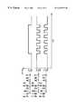
- FIG. 1is a block diagram showing the structure of a conventional negative voltage generating circuit.
- the conventional negative voltage generating circuitwill be described with reference to FIG. 1 .
- This conventional negative voltage generating circuitis composed of a voltage dividing circuit 82 , a comparing circuit 3 , an oscillator 4 , a clock buffer 5 , a negative voltage charge pump 6 .
- the voltage dividing circuit 82divides a voltage between a negative voltage 104 and a power supply voltage Vcc to output a divided voltage 102 .
- the comparing circuit 3compares a voltage value of a reference voltage 120 with a voltage value of the divided voltage 102 .
- the comparing circuit 3sets an oscillator control signal 103 to an active state when the voltage value of the divided voltage 102 is equal to or higher than that of the reference voltage 120 , and sets the oscillator control signal 103 to an inactive state when the voltage value of the divided voltage 102 is lower than that of the reference voltage 120 .
- the comparing circuit 3is composed of a resistor 97 , P-channel MOS transistors 91 and 92 of a current mirror circuit, a P-channel MOS transistor 93 whose gate receives the reference voltage 120 , a P-channel MOS transistor 94 whose gate receives the divided voltage 102 , N-channel MOS transistors 95 and 96 of a current mirror circuit and an inverter 98 .
- the P-channel MOS transistor 91a current determined based on the property thereof and the resistor 97 flows between a source and a drain of the transistor 91 .
- the current having the same current value as that flowing through the transistor 91flows between a source and a drain of the P-channel MOS transistor 92 , which constitutes the current mirror together with the P-channel MOS transistor 91 .
- the P-channel MOS transistor 92functions as a current source that supplies the current to the P-channel MOS transistors 93 and 94 .
- the N-channel MOS transistors 95 and 96 constituting the current mirror circuitare respectively connected to the P-channel MOS transistors 93 and 94 as the loads thereto.
- the voltage supplied to the inverter 98is changed in a range of a certain amplitude, in accordance with whether the divided voltage 102 is higher or lower than the reference voltage 120 .
- the oscillator control signal 103can be generated to indicate whether the divided voltage 102 is higher or lower than the reference voltage 120 .
- the oscillator 4generates and outputs two oscillator output signals 105 and 106 whose phases become opposite to each other, when the oscillator control signal 103 is in the active state. A specific structure of the oscillator 4 will be described with reference to FIG. 3 .
- the oscillator 4is a ring oscillator composed of a NAND circuit 110 and inverters 111 1 to 111 6 .
- the NAND circuit 110is provided in a loop of this ring oscillator.
- the oscillator control signal 103is supplied to one input terminal of the NAND circuit 110 .
- the oscillator control signal 103is used to stop the operation of the oscillator 4 , when the oscillator control signal 103 is in the inactive state of a low level.
- the inverters 111 1 to 111 6are connected in series in the form of a ring. An output of the inverter 111 6 is outputted as an oscillator output signal 105 , and an output of the inverter 111 5 is outputted as an oscillator output signal 106 .
- FIGS. 4A to 4 Care timing charts showing operations of the oscillator control signal 103 and the oscillator output signals 105 and 106 .
- Vccthe two oscillator output signals 105 and 106 whose phases are opposite to each other are outputted, and when the oscillator control signal 103 is in the inactive state of a low level, GND, the oscillator output signals 105 and 106 are not outputted.
- the clock buffer 5receives the oscillator output signals 105 and 106 outputted from the oscillator 4 , and then outputs as complementary pulse signals 107 and 108 though inverters 121 and 122 and inverters 123 and 124 , respectively.
- the negative voltage charge pump 6generates and outputs the negative voltage 104 from the complementary pulse signals 107 and 108 . A specific structure of the negative voltage charge pump 6 will be described with reference to FIG. 6 .
- the negative voltage charge pump 6is composed of P-channel MOS transistors 131 1 to 131 6 , capacitors 132 1 , to 132 6 and a P-channel MOS transistor 133 .
- the P-channel MOS transistors 131 1 , to 131 6are connected in series such that a gate and a source of each P-channel MOS transistor are connected to each other and further a source of one transistor and a drain of another transistor are connected to each other between the transistors adjacent to each other.
- the drains of the P-channel MOS transistors 131 1 , 131 3 and 131 5are connected to the complementary pulse signal 107 through the capacitors 132 1 , 132 3 and 132 5 , respectively. Also, the drains of the P-channel MOS transistors 131 2 , 131 4 and 131 6 are connected to the complementary pulse signal 108 through the capacitors 132 2 , 132 4 and 132 6 , respectively.
- the source of the P-channel MOS transistor 131 1is outputted as the negative voltage 104
- the drain of the P-channel MOS transistor 131 6is connected to the source of the P-channel MOS transistor 133 .
- the gate and drain of the P-channel MOS transistor 133are connected to the ground to set the drain of the P-channel MOS transistor 131 6 to a ground potential.
- the complementary pulse signal 107is set to the power supply voltage Vcc and the complementary pulse signal 108 is set to the ground potential.
- the potential of the node 13 ais set to the high level.
- the node 13 bis lowered by the capacitor 132 2 , the potential of the node 13 b is set to the low level.
- the P-channel MOS transistor 131 2is in an ON state. At this time, he charges of the node 13 a flow into the node 13 b whose potential is in the low level.
- the potentialis made lower. Also, as the charges are increased at the node 13 b , the potential is made higher. Then, the movement of the charges is continued until the potential of the node 13 a becomes equal to that of the node 13 b.
- the complementary pulse signal 107is set to the ground potential, and the complementary pulse signal 108 is set to the power supply voltage Vcc.
- the potential of the node 13 ais set to the low level.
- the potential of the node 13 bis set to the high level. Even if the potential of the node 13 b is increased to high level, the gate and the drain maintain the same potential because the gate and the drain are connected to each other. Thus, the P-channel MOS transistor 131 2 remains in the OFF state. However, the above mentioned movement of the charges is performed in the P-channel MOS transistors 131 1 and 131 3 which are adjacent to the P-channel MOS transistor 131 2 .
- the complementary pulse signals 107 and 108are alternately switched between the power supply potential level and the ground potential level, and further the P-channel MOS transistors 131 1 , to 131 6 repeat the above mentioned operation. Accordingly, the charges are sequentially transferred in the direction from the P-channel MOS transistor 131 1 to the P-channel MOS transistor 131 6 .
- the source of the P-channel MOS transistor 131 1is set to the lowest potential in the negative voltage charge pump 6 , and outputted as the negative voltage 104 .
- the comparing circuit 3sets the oscillator control signal 103 to the active state.
- the oscillator 4generates and outputs the oscillator output signals 105 and 106 in response to the active oscillator control signal 103 .
- the clock buffer 5receives the oscillator output signals 105 and 106 , and then outputs the complementary pulse signals 107 and 108 .
- the negative voltage charge pump 6functions to decrease the voltage value of the negative voltage 104 .
- the oscillator 4When the negative voltage 104 reaches the desired voltage so that the divided voltage 102 outputted from the voltage dividing circuit 82 becomes equal to the reference voltage 120 , the oscillator 4 does not output the oscillator output signals 105 and 106 , because the comparing circuit 3 sets the oscillator control signal 103 to inactive state.
- the negative voltage charge pump 6stops the operation in response to the inactive oscillator control signal 103 . Also, the voltage value of the negative voltage 104 remains in the defined voltage value.
- the thus-generated negative voltage 104is used to erase the content stored in the flash memory.
- another problemoccurs that as the negative voltage 104 is made higher, the erasing time in a memory cell is increased longer. On the other hand, when the negative voltage 104 is made lower, the erasing time becomes shorter.
- another problemoccurs of reliability, such as a deterioration of a data retaining property of the memory cell.
- the optimal voltage valuebecomes a limited voltage value, in view of these conditions. Hence, the optimal operation for the flash memory requires that the voltage value of the negative voltage 104 has a high accuracy.
- the power supply voltage Vcc and the negative voltage 104are divided by the voltage dividing circuit 82 to generate the divided voltage 102 .
- the voltage value of the power supply voltage Vcc externally appliedis different on the basis of the used situation. Hence, the high accuracy can not be attained in the voltage value of the negative voltage 104 .
- this negative voltage generating circuit shown in FIG. 7requires that a negative potential is supplied to the comparing circuit 3 as the reference voltage 120 . This results in a complex circuit structure of the comparing circuit 3 .
- an object of the present inventionis to provide a negative voltage generating circuit which can generate a negative voltage with a high accuracy without requiring a complex circuit.
- a negative voltage generating circuitincludes a reference voltage generating circuit for generating a first reference voltage, voltage dividing circuit for dividing a voltage between the first reference voltage and a negative voltage to produce a division voltage, a comparing circuit for comparing a second reference voltage and the division voltage, and a negative voltage generating section for generating the negative voltage based on the comparing result by the comparing circuit to supply to the voltage dividing circuit.
- the voltage dividing circuitmay include a first resistor section connected to the first reference voltage and a second resistor section connected to the first resistor section and the negative voltage.
- the first resistor sectionmay include at least one first resistor element
- the second resistor sectionmay include at least one second resistor element which has a same resistance as the first resistor element.
- it is desirable that the first and second resistor sectionsare formed as first and second diffusion layers in a first well of a first conductive type which is formed in a semiconductor region having a second conductive type different from the first conductive type.
- the first diffusion layeris connected to the first reference voltage at a first end, a second end of the first diffusion layer and a first end of the second diffusion layer are connected to output the division voltage, a second end of the second diffusion layer is connected to the negative voltage, and the first well is connected to one of a positive power supply voltage and the negative voltage based on the first conductive type.
- the first and second resistor sectionsmay be formed as first and second diffusion layers in a first well of a first conductive type which is formed in a second well having a second conductive type different from the first conductive type, the second well being formed in a semiconductor region of the first conductive type.
- the first diffusion layeris connected to the first reference voltage at a first end, a second end of the first diffusion layer and a first end of the second diffusion layer are connected to output the division voltage, a second end of the second diffusion layer is connected to the negative voltage, and the first well is connected to one of a positive power supply voltage and the negative voltage based on the first conductive type, and the second well is connected to the other of the positive power supply voltage and the negative voltage based on the first conductive type.
- the voltage dividing circuitmay include a plurality of MOS transistors connected in series.
- a source of a first one of the MOS transistorsis connected to the first reference voltage and a drain of a last one of the MOS transistors is connected to the negative voltage.
- a source and gate of each of the plurality MOS transistorsare connected to each other and a drain and well contact of the MOS transistor are connected to each other, and the drain of the MOS transistor is connected to a source of a next one of the plurality of MOS transistors.
- Each of the plurality of MOS transistorsis desirably formed in a first well of first conductive type which is formed in a second well of a second conductive type which is formed in a semiconductor region of the first conductive type, and the second well is desirably connected to one of a positive power supply voltage and the negative voltage based on the first conductive type.
- the voltage dividing circuitmay include a first group of MOS transistors connected in series and a second group of MOS transistor circuits, the second group being connected to the first group in series.
- Each of the MOS transistor circuitsmay include a first set of a first MOS transistor and a first switch which are connected in series, a second set of a second MOS transistor and a second switch which are connected in series, and a third set of a third switch, the first to third sets are connected in parallel.
- a first one of the MOS transistors of the first groupis connected to the reference voltage and a last one of the sets of the second group is connected to the negative voltage.
- the voltage dividing circuit and the comparing circuitare desirably arranged to be adjacent to each other and connected to a ground potential pad.
- a method of generating a negative voltage in a semiconductor deviceincludes the steps of:
- the internal voltageis generated from a power supply voltage. Also, the division voltage is 0 when the negative voltage reaches a desired value.
- a negative voltage generating circuitincludes a reference voltage generating circuit for generating a reference voltage, a voltage dividing circuit for dividing a voltage between the reference voltage and a negative voltage to produce a division voltage, a comparing circuit for comparing a ground potential and a potential corresponding to the division voltage, and a negative voltage generating section for generating the negative voltage based on the comparing result by the comparing circuit to supply to the voltage dividing circuit.
- FIG. 1is a block diagram showing the structure of a conventional negative voltage generating circuit
- FIG. 2is a circuit diagram showing the structure of a comparing circuit 3 of the conventional negative voltage generating circuit shown in FIG. 1;
- FIG. 3is a circuit diagram showing the structure of an oscillator 4 of the conventional negative voltage generating circuit shown in FIG. 1;
- FIGS. 4A to 4 Care timing charts to show signal waves of the oscillator 4 of the conventional negative voltage generating circuit
- FIG. 5is a circuit diagram showing the structure of a clock buffer 5 of the conventional negative voltage generating circuit shown in FIG. 1;
- FIG. 6is a circuit diagram showing the structure of a negative voltage charge pump 6 of the conventional negative voltage generating circuit shown in FIG. 1;
- FIG. 7is a block diagram showing the structure of another conventional negative voltage generating circuit
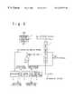
- FIG. 8is a block diagram showing the structure of a negative voltage generating circuit in a first embodiment of the present invention.
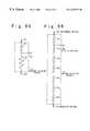
- FIG. 9Ais a circuit diagram when a voltage dividing circuit 2 a of the negative voltage generating circuit in the first embodiment of the present invention.
- FIG. 9Bis a circuit diagram when another voltage dividing circuit 2 b of the negative voltage generating circuit in the first embodiment of the present invention.
- FIG. 10Ais a section view of the voltage dividing circuit 2 a of FIG. 9A constituted to have a twin well structure;
- FIG. 10Bis a section view of the voltage dividing circuit 2 b of FIG. 9 b constituted to have a triple well structure
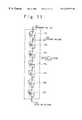
- FIG. 11is a circuit diagram of the structure of a voltage dividing circuit 2 c in the negative voltage generating circuit according to a second embodiment of the present invention.
- FIG. 12is a section view of the voltage dividing circuit 2 c of FIG. 11 constituted to have a triple well structure
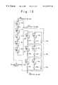
- FIG. 13is a circuit diagram of a voltage dividing circuit 2 d in the negative voltage generating circuit according to a third embodiment of the present invention.
- FIG. 14is a view showing a wiring pattern arrangement in the negative voltage generating circuit according to a fourth embodiment of the present invention.
- FIG. 8is a block diagram showing a structure of the negative voltage generating circuit according to the first embodiment of the present invention.
- the numerals similar to those in FIG. 1denote similar components.
- the negative voltage generating circuit in the first embodimentis composed of a reference voltage generating circuit 1 , a voltage dividing circuit 2 , a comparing circuit 3 , and a negative voltage generating section which is composed of an oscillator 4 , a clock buffer 5 , a negative voltage charge pump 6 .
- the reference voltage generating circuit 1generates a constant voltage having a voltage value between the power supply voltage Vcc and the ground, and then outputs a reference voltage 101 to the voltage dividing circuit 2 .
- the voltage dividing circuit 2divides a difference voltage between the reference voltage 101 outputted from the reference voltage generator 1 and the negative voltage 104 , and then outputs the divided voltage as the divided voltage 102 .
- this voltage dividing circuit 2it is assumed that the divided voltage 102 is equal to the ground potential when the negative voltage 104 becomes equal to a desired voltage value. Therefore, the voltage dividing circuit 2 can generate the divided voltage 102 without receiving the influence of the variation of the power supply voltage Vcc.
- the comparing circuit 3compares a voltage value of a reference voltage with a voltage value of the divided voltage 102 .
- the comparing circuit 3sets an oscillator control signal 103 to an active state when the voltage value of the divided voltage 102 is equal to or higher than that of the reference voltage (0 V in this example), and sets the oscillator control signal 103 to an inactive state when the voltage value of the divided voltage 102 is lower than that of the reference voltage.
- the voltage dividing circuit 2is designed in such a manner that the divided voltage 102 outputted by the voltage dividing circuit 2 becomes equal to the ground potential when the negative voltage 104 is equal to the desired negative voltage. Therefore, it is sufficient for the comparing circuit 3 to compare the divided voltage 104 with the ground potential to generate the oscillator control signal 103 . Hence, it is not necessary that the complex circuit is used in the comparing circuit 3 .
- the oscillator 4generates and outputs two oscillator output signals 105 and 106 whose phases become opposite to each other, when the oscillator control signal 103 is in the active state.
- the clock buffer 5receives the oscillator output signals 105 and 106 outputted from the oscillator 4 , and then outputs complementary pulse signals 107 and 108 though inverters 121 and 122 and inverters 123 and 124 , respectively.
- the negative voltage charge pump 6generates and outputs the negative voltage 104 from the complementary pulse signals 107 and 108 .
- comparing circuit 3oscillator 4 , clock buffer 5 and negative voltage charge pump 6 are similar to those shown in FIGS. 2, 3 , 5 , and 6 . Therefore, the descriptions are omitted.
- FIGS. 9A and 9Bshow examples in which the voltage dividing circuit 2 is constituted by using a resistor division circuit.
- FIG. 9Ashows a voltage dividing circuit 2 a as a specific example of the voltage dividing circuit 2 .
- the voltage dividing circuit 2 ais composed of two resistors 21 and 22 which are connected in series and have values different from each other. In the voltage dividing circuit 2 a , the respective values of the two resistors 21 and 22 are changed such that the divided voltage 102 is equal to the ground potential when the desired negative voltage 104 is attained.
- FIG. 9Bshows a voltage dividing circuit 2 b as another specific example of the voltage dividing circuit 2 .
- this voltage dividing circuit 2 bseven resistors 231 to 237 having the same value are connected in series.
- the number of resistors to be connectedis changed such that the divided voltage 102 becomes equal to the ground potential when the desired negative voltage 104 is attained.
- FIGS. 10A and 10Bshow section views of a semiconductor structure of the voltage dividing circuit 2 a shown in FIG. 9 A.
- FIG. 10Ashows a case in which the voltage dividing circuit 2 a is constituted by a twin well structure.
- FIG. 10Bshows a case in which the voltage dividing circuit 2 a is constituted by a triple well structure.
- an N well 34is formed in a P type substrate 31 , and P type impurity diffusion layers 32 and 33 are formed in the surface of the N well 34 .
- the reference voltage 101is applied to one end of the P type impurity diffusion layer 32 , and the other end is connected to one of the P type impurity diffusion layer 33 .
- the divided voltage 102is outputted therefrom.
- the negative voltage 104is applied to the other end of the P type impurity diffusion layer 33 .
- the power supply voltage Vccis applied to the N well 34 through an N well contact 39 .
- the P type substrate 31is connected to the ground.
- the P type substrate 31 and the N well 34are electrically insulated from each other.
- the reference voltage 101 applied to the P type impurity diffusion layer 32 and the negative voltage 104 applied to the P type impurity diffusion layer 33are lower than the power supply voltage Vcc.
- each of the P type impurity diffusion layers 32 and 33 and the N well 34are electrically insulated from each other.
- the resistor 21is formed of the P type impurity diffusion layer 32
- the resistor 22is formed of the P type impurity diffusion layer 33 .
- the electrically conductive properties of the P type impurity diffusion layers 32 and 33are determined based on the densities of the diffused impurity ions, the diffusion depths and areas.
- the densities of the diffused impurity in the P type impurity diffusion layers 32 and 33 , the diffusion depths and areasare adjusted to determine the values of the resistors such that the divided voltage 102 is equal to the ground potential, when the negative voltage 104 becomes equal to the desired voltage value.
- an N well 37is formed in a P type substrate 31
- a P well 38is formed in the N well 37
- N type impurity diffusion layers 35 and 36are formed in the surface of the P well 38 .
- the reference voltage 101is applied to one end of the N type impurity diffusion layer 35
- the other end of the N type impurity diffusion layer 35is connected to one end of the N type impurity diffusion layer 36 .
- the divided voltage 102is outputted therefrom.
- the negative voltage 104is applied to the other end of the N type impurity diffusion layer 36 .
- the power supply voltage Vccis applied to the N well 37 through an N well contact 40 .
- the P type substrate 31is connected to the ground.
- the P type substrate 31 and the N well 37are electrically insulated from each other.
- the negative voltage 104 applied to the P well 38is lower than the power supply voltage Vcc.
- the P well 38 and the N well 37are electrically insulated from each other.
- the values of the resistorsare determined by the manner similar to that in FIG. 10 A.
- the triple well structure shown in FIG. 10Bhas a demerit that the area is increased because margin is required when master patterns of the N well 37 and the P well 38 are designed.
- the triple well structurehas a merit that the potential difference between junction is made smaller as compared with the twin well structure.
- a voltage between the negative voltage 104 and the N well 34 whose potential is equal to the power supply voltage Vccis the highest voltage between the junction.
- this voltageis 17 V if the power supply voltage Vcc is 5 V and the negative voltage 104 is ⁇ 12 V.
- a voltage between the reference voltage 101 and the P well 38 whose potential is equal to the negative voltage 104is the highest voltage between the junction.
- This voltageis 14 V, which is lower than 17 V, if the reference voltage 101 is 2 V and the negative voltage 104 is ⁇ 12 V. In this way, the potential difference between the junction can be made smaller in the triple well structure.
- the voltage dividing circuit 2 a shown in FIG. 9Awill be described.
- the voltage dividing circuit 2 b shown in FIG. 9Bcan be similarly constituted by using the twin well structure or the triple well structure.
- a plurality of resistors having the same sizeare formed in this case.
- these values of the resistors having the same sizeare varied in the same direction, even if a mask pattern, the impurity density, the diffusion depth and area are varied.
- the voltage dividing circuit with the high accuracycan be attained in the case where the plurality of resistors having the same size are provided and the voltage is divided using the plurality of resistors, as compared with a case where a voltage is divided using the resistors whose sizes are different from each other.
- a negative voltage generating circuit in the second embodimentuses a voltage dividing circuit 2 c shown in FIG. 11 instead of a specific example of the voltage dividing circuit 2 in the first embodiment shown in FIG. 8 .
- the voltage dividing circuit 2is constituted by using the resistor division circuit.
- the reference voltage 101 and the negative voltage 104are divided by using N-channel MOS transistors, and thereby the divided voltage 102 is generated.
- the voltage dividing circuit 2 cseven N-channel MOS transistors 42 1 to 42 7 are connected in series, as shown in FIG. 11 .
- FIG. 12shows a section view of the voltage dividing circuit 2 c in FIG. 11 .
- the seven N-channel MOS transistors 42 1 to 42 7have the same structure. Thus, only the structure of the N-channel MOS transistor 42 1 will be described.
- an N well 55is formed in a P type substrate 56 , P wells 54 are formed in the N well 55 .
- a drain diffusion layer 51 , a source diffusion layer 52 and a P well contact 53are formed in the surface of the P well 54 .
- a gate electrode 58is formed through an insulation film on the P well 54 .
- the gate electrode 58 and the drain diffusion layer 51are connected to each other, and the reference voltage 101 is applied to the gate electrode 58 and the drain diffusion layer 51 .
- the source diffusion layer 52 and the P well contact 53are connected to each other, and further connected to a drain diffusion layer of the N-channel MOS transistor 42 2 adjacent to the N-channel MOS transistor 42 1 .
- the divided voltage 102is outputted from the portion between the N-channel MOS transistor 42 1 and the N-channel MOS transistor 42 2 .
- the power supply voltage Vccis applied through a N well contact 57 to the N well 55 .
- this N-channel MOS transistor 42 1is set to a conductive state. Thus, a current begins to flow.
- the threshold voltagebe 1 V. Since the voltage dividing circuit 2 c in FIG. 11 is composed of the seven N-channel MOS transistors 42 1 to 42 7 , the current begins to flow, when the potential difference between the reference voltage 101 and the negative voltage 104 is equal to or greater than 7 V. Then, the voltage dividing circuit 2 c starts the operation as the voltage dividing circuit. At this time, the same current flows through all the N-channel MOS transistors 42 1 to 42 7 . Thus, the potential difference between the gate electrode 58 and the source diffusion layer 52 is the same voltage even in any of the N-channel MOS transistors 42 1 to 42 7 . Since each source diffusion layer 52 is connected to the P well 54 through the P well contact 53 , there is no variation of the threshold voltage due to the substrate influence.
- the voltage dividing circuit having the high accuracycan be attained with low consumption current and the small block size, if all mutual conductances gm of the N-channel MOS transistors 42 1 to 42 7 are equally designed.
- the N-channel MOS transistors 42 1 to 42 7 having the same sizeare connected in series, similarly to the voltage dividing circuit 2 b using the resistor division shown in FIG. 9 B.
- the values of the resistorsare varied in the same direction even if the mask patterns, the impurity densities, the diffused depths and area are varied.
- the voltage dividing circuit with the high accuracycan be attained, as compared with the manner of dividing by using the N-channel MOS transistors whose sizes are different from each other.
- the negative voltage generating circuit in the third embodimentuses a voltage dividing circuit 2 d shown in FIG. 13 as a specific example of the voltage dividing circuit 2 shown in FIG. 8 .
- This voltage dividing circuit 2 dcomposed of N-channel MOS transistors 42 1 to 42 8 and 62 6 to 62 8 divides a voltage between the reference voltage 101 and the negative voltage 104 , similarly to the voltage dividing circuit 2 c in the second embodiment. Also, switches 64 1 to 64 9 are disposed to set the divided voltage to the desired negative voltage 104 .
- Mutual conductances gm of the N-channel MOS transistors 62 6 to 62 8are designed to be larger than mutual conductances gm of the N-channel MOS transistors 42 1 to 42 8 . Also, a voltage between a source and drain of each of the N-channel MOS transistors 62 6 to 62 8 is set to be half of that of each of the N-channel MOS transistors 42 1 to 42 8 .
- the voltage dividing circuit 2 dbecomes similar to the voltage dividing circuit 2 c shown in FIG. 11 .
- the divided voltage 102is equal to the ground potential.
- the switches 62 1 , 62 4 and 62 8are turned on and the other switches are turned off when the negative voltage 104 is ⁇ 13 V, the divided voltage 102 is equal to the ground potential.
- the switches 64 1 to 64 9are switched as shown in the following table 1, when the reference voltage 101 is 2 V, the voltage value which can be set as the negative voltage 104 can be selected at a step of 1 V between ⁇ 8 and ⁇ 14 V. In this manner, in this embodiment, the voltage value of the desired negative voltage 104 can be selected by switching the connections of the N-channel MOS transistors by using the switches.
- a ground pattern of the reference voltage generator 1 and a ground pattern of the comparing circuit 3are connected to a common ground pad and the reference voltage generator 1 and the comparing circuit 3 are provided on positions where properties such as values of current flowing out from the ground pad are substantially equal to each other, in the negative voltage generating circuits of the first to third embodiments.
- the reference voltage generator 1 and the comparing circuit 3are arranged to have the above mentioned positional relation, the deviation of the voltage can be canceled between the reference voltage generator 1 and the comparing circuit 3 .
- the negative voltage 104 with the high accuracycan be attained in addition to the effects of the first to third embodiments.
- the reference voltage generator 1 and the comparing circuit 3are arranged on positions A and B as shown in FIG. 14 and are connected to a ground pattern 71 .
- the above mentioned conditionis satisfied.
- the reference voltage generator 1 and the comparing circuit 3are arranged on positions A and C or positions B and C, the above mentioned condition is not satisfied.
- the negative voltage with the high accuracycan be generated without requiring a complex circuit.
Landscapes
- Engineering & Computer Science (AREA)
- Power Engineering (AREA)
- Semiconductor Integrated Circuits (AREA)
- Dram (AREA)
Abstract
Description
| TABLE 1 | |||||||||
| Volt | |||||||||
| 104 | |||||||||
| (V) | SW647 | SW648 | SW649 | SW644 | SW645 | SW646 | SW641 | SW642 | SW643 |
| −14 | ON | OFF | OFF | ON | OFF | OFF | ON | OFF | OFF |
| −13 | OFF | ON | OFF | ON | OFF | OFF | ON | OFF | OFF |
| −12 | OFF | OFF | ON | ON | OFF | OFF | ON | OFF | OFF |
| −11 | OFF | OFF | ON | OFF | ON | OFF | ON | OFF | OFF |
| −10 | OFF | OFF | ON | OFF | OFF | ON | ON | OFF | OFF |
| −9 | OFF | OFF | ON | OFF | OFF | ON | OFF | ON | OFF |
| −8 | OFF | OFF | ON | OFF | OFF | ON | OFF | OFF | ON |
Claims (11)
Applications Claiming Priority (2)
| Application Number | Priority Date | Filing Date | Title |
|---|---|---|---|
| JP31525597AJP3278765B2 (en) | 1997-11-17 | 1997-11-17 | Negative voltage generation circuit |
| JP9-315255 | 1997-11-17 |
Publications (1)
| Publication Number | Publication Date |
|---|---|
| US6229379B1true US6229379B1 (en) | 2001-05-08 |
Family
ID=18063237
Family Applications (1)
| Application Number | Title | Priority Date | Filing Date |
|---|---|---|---|
| US09/190,445Expired - LifetimeUS6229379B1 (en) | 1997-11-17 | 1998-11-13 | Generation of negative voltage using reference voltage |
Country Status (5)
| Country | Link |
|---|---|
| US (1) | US6229379B1 (en) |
| JP (1) | JP3278765B2 (en) |
| KR (1) | KR100337999B1 (en) |
| CN (1) | CN1160861C (en) |
| TW (1) | TW427070B (en) |
Cited By (35)
| Publication number | Priority date | Publication date | Assignee | Title |
|---|---|---|---|---|
| US20010045841A1 (en)* | 2000-05-22 | 2001-11-29 | Matsushita Electric Industria Co., Ltd. | Semiconductor integrated circuit, test method for the same, and recording device and communication equipment having the same |
| US6593779B2 (en)* | 1999-11-30 | 2003-07-15 | Xilinx, Inc. | Tunable circuit for detection of negative voltages |
| US20040128566A1 (en)* | 2002-12-31 | 2004-07-01 | Burr James B. | Adaptive power control |
| US6861895B1 (en)* | 2003-06-17 | 2005-03-01 | Xilinx Inc | High voltage regulation circuit to minimize voltage overshoot |
| US20060103434A1 (en)* | 2004-11-17 | 2006-05-18 | Renesas Technology Corp. | Semiconductor device |
| US20070153522A1 (en)* | 2006-01-03 | 2007-07-05 | Helget Gerald E | Identification and/or trail light |
| US20070273433A1 (en)* | 2006-05-24 | 2007-11-29 | Choy Jon S | Floating voltage source |
| US20080252362A1 (en)* | 2007-04-11 | 2008-10-16 | Au Optronics Corp. | Negative voltage converter |
| US20090153237A1 (en)* | 2007-12-12 | 2009-06-18 | Micron Technology, Inc. | Compensation capacitor network for divided diffused resistors for a voltage divider |
| US7649402B1 (en) | 2003-12-23 | 2010-01-19 | Tien-Min Chen | Feedback-controlled body-bias voltage source |
| US20100073032A1 (en)* | 2008-09-19 | 2010-03-25 | Seiko Epson Corporation | Voltage comparator and electronic device |
| US7692477B1 (en) | 2003-12-23 | 2010-04-06 | Tien-Min Chen | Precise control component for a substrate potential regulation circuit |
| US7719344B1 (en)* | 2003-12-23 | 2010-05-18 | Tien-Min Chen | Stabilization component for a substrate potential regulation circuit |
| US7733126B1 (en) | 2009-03-31 | 2010-06-08 | Freescale Semiconductor, Inc. | Negative voltage generation |
| US7774625B1 (en) | 2004-06-22 | 2010-08-10 | Eric Chien-Li Sheng | Adaptive voltage control by accessing information stored within and specific to a microprocessor |
| US7847619B1 (en) | 2003-12-23 | 2010-12-07 | Tien-Min Chen | Servo loop for well bias voltage source |
| US20100327846A1 (en)* | 2009-06-25 | 2010-12-30 | Nec Electronics Corporation | Semiconductor apparatus |
| US7953990B2 (en) | 2002-12-31 | 2011-05-31 | Stewart Thomas E | Adaptive power control based on post package characterization of integrated circuits |
| CN102213967A (en)* | 2010-04-12 | 2011-10-12 | 辉达公司 | GPU (Graphics Processing Unit) chip with voltage adjusting function and manufacturing method thereof |
| US8370658B2 (en) | 2004-06-22 | 2013-02-05 | Eric Chen-Li Sheng | Adaptive control of operating and body bias voltages |
| US8442784B1 (en) | 2002-12-31 | 2013-05-14 | Andrew Read | Adaptive power control based on pre package characterization of integrated circuits |
| US20130264645A1 (en)* | 2006-08-24 | 2013-10-10 | Infineon Technologies Ag | Diode Biased ESD Protection Device and Method |
| US20160085254A1 (en)* | 2014-09-22 | 2016-03-24 | Integrated Solutions Technology Inc. | Multi-stage voltage division circuit |
| US9407241B2 (en) | 2002-04-16 | 2016-08-02 | Kleanthes G. Koniaris | Closed loop feedback control of integrated circuits |
| US20160380632A1 (en)* | 2014-09-30 | 2016-12-29 | Skyworks Solutions, Inc. | Voltage generator with charge pump and related methods and apparatus |
| US9785177B1 (en) | 2016-08-03 | 2017-10-10 | Nxp Usa, Inc. | Symmetrical positive and negative reference voltage generation |
| US9847774B2 (en) | 2014-08-07 | 2017-12-19 | Skyworks Solutions, Inc. | Apparatus and methods for level shifting in a radio frequency system |
| KR20180003432A (en)* | 2016-06-30 | 2018-01-09 | 가부시키가이샤 한도오따이 에네루기 켄큐쇼 | Semiconductor device and method for operating the semiconductor device |
| US10236875B2 (en) | 2016-04-15 | 2019-03-19 | Semiconductor Energy Laboratory Co., Ltd. | Semiconductor device and method for operating the semiconductor device |
| US10250247B2 (en) | 2016-02-10 | 2019-04-02 | Semiconductor Energy Laboratory Co., Ltd. | Semiconductor device, electronic component, and electronic device |
| CN110660443A (en)* | 2018-06-29 | 2020-01-07 | 台湾积体电路制造股份有限公司 | Assist circuit, memory system and method for assisting reading to multiple memory units |
| US10855176B1 (en) | 2019-05-15 | 2020-12-01 | Samsung Electro-Mechanics Co., Ltd. | Negative voltage generation circuit without low-dropout regulator |
| US10944396B2 (en) | 2017-03-03 | 2021-03-09 | Semiconductor Energy Laboratory Co., Ltd. | Semiconductor device and method for driving the semiconductor device |
| CN114333926A (en)* | 2022-01-27 | 2022-04-12 | 珠海博雅科技股份有限公司 | Standby working negative pressure generating circuit and non-volatile memory |
| US11457167B2 (en) | 2017-05-31 | 2022-09-27 | Semiconductor Energy Laboratory Co., Ltd. | Comparison circuit, semiconductor device, electronic component, and electronic device |
Families Citing this family (16)
| Publication number | Priority date | Publication date | Assignee | Title |
|---|---|---|---|---|
| JP3604991B2 (en) | 2000-03-14 | 2004-12-22 | Necエレクトロニクス株式会社 | Low power supply voltage detection circuit |
| JP5102413B2 (en)* | 2000-07-12 | 2012-12-19 | ユナイテッド・マイクロエレクトロニクス・コーポレイション | Apparatus for generating a second power supply voltage from a first power supply voltage, a reference voltage generator, and a method and apparatus for generating a desired voltage |
| JP2002208275A (en)* | 2001-01-11 | 2002-07-26 | Matsushita Electric Ind Co Ltd | Semiconductor integrated circuit and inspection method thereof |
| US7336121B2 (en)* | 2001-05-04 | 2008-02-26 | Samsung Electronics Co., Ltd. | Negative voltage generator for a semiconductor memory device |
| JP4274786B2 (en)* | 2002-12-12 | 2009-06-10 | パナソニック株式会社 | Voltage generation circuit |
| JP2006129127A (en)* | 2004-10-29 | 2006-05-18 | Olympus Corp | Voltage supply circuit and solid-state image pickup device using the same |
| ATE420395T1 (en)* | 2004-11-18 | 2009-01-15 | Nxp Bv | REFERENCE VOLTAGE CIRCUIT |
| JP5315604B2 (en)* | 2006-09-29 | 2013-10-16 | 富士通セミコンダクター株式会社 | Semiconductor integrated circuit |
| JP5369413B2 (en)* | 2007-09-14 | 2013-12-18 | 富士電機株式会社 | Semiconductor device |
| JP5590802B2 (en)* | 2008-04-11 | 2014-09-17 | ピーエスフォー ルクスコ エスエイアールエル | Basic cell and semiconductor device |
| JP5376516B2 (en)* | 2009-07-27 | 2013-12-25 | スパンション エルエルシー | Semiconductor device |
| CN102647082B (en)* | 2012-04-24 | 2017-02-08 | 上海华虹宏力半导体制造有限公司 | Negative voltage generation circuit |
| KR101382546B1 (en)* | 2012-11-26 | 2014-04-07 | 순천향대학교 산학협력단 | Pulse type power supply circuit with bipolar variable output voltage |
| CN106549572B (en)* | 2016-10-27 | 2019-08-16 | 昆山龙腾光电有限公司 | A kind of circuit for generating negative voltage |
| CN110348432A (en)* | 2018-04-01 | 2019-10-18 | 印芯科技股份有限公司 | Optical recognition module |
| CN115309231B (en)* | 2021-05-08 | 2024-05-10 | 长鑫存储技术有限公司 | Comparison circuit and negative voltage generation system |
Citations (16)
| Publication number | Priority date | Publication date | Assignee | Title |
|---|---|---|---|---|
| JPS57113262A (en) | 1980-12-30 | 1982-07-14 | Seiko Epson Corp | Voltage dividing system for semiconductor integrated circuit |
| JPS57199335A (en) | 1981-06-02 | 1982-12-07 | Toshiba Corp | Generating circuit for substrate bias |
| JPS63166257A (en) | 1986-12-27 | 1988-07-09 | Nec Corp | semiconductor equipment |
| JPH01218211A (en) | 1988-02-26 | 1989-08-31 | Fujitsu Ltd | Reference voltage generating circuit |
| JPH01233752A (en) | 1988-03-14 | 1989-09-19 | Nec Corp | Reference-voltage setting circuit |
| US5113088A (en)* | 1988-11-09 | 1992-05-12 | Oki Electric Industry Co., Ltd. | Substrate bias generating circuitry stable against source voltage changes |
| JPH04146665A (en) | 1990-10-09 | 1992-05-20 | Sony Corp | Resistance element |
| US5355014A (en)* | 1993-03-03 | 1994-10-11 | Bhasker Rao | Semiconductor device with integrated RC network and Schottky diode |
| JPH0778471A (en) | 1993-09-10 | 1995-03-20 | Toshiba Corp | Semiconductor integrated circuit |
| JPH07273287A (en) | 1994-03-28 | 1995-10-20 | Nec Eng Ltd | Semiconductor resistance device and amplifier circuit using it |
| US5483486A (en)* | 1994-10-19 | 1996-01-09 | Intel Corporation | Charge pump circuit for providing multiple output voltages for flash memory |
| US5553295A (en)* | 1994-03-23 | 1996-09-03 | Intel Corporation | Method and apparatus for regulating the output voltage of negative charge pumps |
| US5554873A (en)* | 1994-05-23 | 1996-09-10 | Texas Instruments Incorporated | Semiconductor device having polysilicon resistor with low temperature coefficient |
| JPH0951266A (en) | 1995-03-14 | 1997-02-18 | Lattice Semiconductor Corp | Circuit and method for maintaining substrate voltage to desired value |
| US5640118A (en)* | 1994-04-21 | 1997-06-17 | Sgs-Thomson Microelectronics S.A. | Voltage-limiting circuit with hysteresis comparator |
| US5661332A (en)* | 1994-01-27 | 1997-08-26 | Nippondenso Co., Ltd. | Semiconductor diffused resistor |
Family Cites Families (1)
| Publication number | Priority date | Publication date | Assignee | Title |
|---|---|---|---|---|
| JP2604074B2 (en)* | 1991-07-26 | 1997-04-23 | 株式会社テック | Power supply |
- 1997
- 1997-11-17JPJP31525597Apatent/JP3278765B2/ennot_activeExpired - Lifetime
- 1998
- 1998-10-27TWTW087117805Apatent/TW427070B/ennot_activeIP Right Cessation
- 1998-11-13USUS09/190,445patent/US6229379B1/ennot_activeExpired - Lifetime
- 1998-11-16KRKR1019980049135Apatent/KR100337999B1/ennot_activeExpired - Fee Related
- 1998-11-17CNCNB981248365Apatent/CN1160861C/ennot_activeExpired - Lifetime
Patent Citations (18)
| Publication number | Priority date | Publication date | Assignee | Title |
|---|---|---|---|---|
| JPS57113262A (en) | 1980-12-30 | 1982-07-14 | Seiko Epson Corp | Voltage dividing system for semiconductor integrated circuit |
| JPS57199335A (en) | 1981-06-02 | 1982-12-07 | Toshiba Corp | Generating circuit for substrate bias |
| US4471290A (en)* | 1981-06-02 | 1984-09-11 | Tokyo Shibaura Denki Kabushiki Kaisha | Substrate bias generating circuit |
| JPS63166257A (en) | 1986-12-27 | 1988-07-09 | Nec Corp | semiconductor equipment |
| JPH01218211A (en) | 1988-02-26 | 1989-08-31 | Fujitsu Ltd | Reference voltage generating circuit |
| JPH01233752A (en) | 1988-03-14 | 1989-09-19 | Nec Corp | Reference-voltage setting circuit |
| US5113088A (en)* | 1988-11-09 | 1992-05-12 | Oki Electric Industry Co., Ltd. | Substrate bias generating circuitry stable against source voltage changes |
| JPH04146665A (en) | 1990-10-09 | 1992-05-20 | Sony Corp | Resistance element |
| US5355014A (en)* | 1993-03-03 | 1994-10-11 | Bhasker Rao | Semiconductor device with integrated RC network and Schottky diode |
| JPH0778471A (en) | 1993-09-10 | 1995-03-20 | Toshiba Corp | Semiconductor integrated circuit |
| US5661332A (en)* | 1994-01-27 | 1997-08-26 | Nippondenso Co., Ltd. | Semiconductor diffused resistor |
| US5553295A (en)* | 1994-03-23 | 1996-09-03 | Intel Corporation | Method and apparatus for regulating the output voltage of negative charge pumps |
| JPH07273287A (en) | 1994-03-28 | 1995-10-20 | Nec Eng Ltd | Semiconductor resistance device and amplifier circuit using it |
| US5640118A (en)* | 1994-04-21 | 1997-06-17 | Sgs-Thomson Microelectronics S.A. | Voltage-limiting circuit with hysteresis comparator |
| US5554873A (en)* | 1994-05-23 | 1996-09-10 | Texas Instruments Incorporated | Semiconductor device having polysilicon resistor with low temperature coefficient |
| US5483486A (en)* | 1994-10-19 | 1996-01-09 | Intel Corporation | Charge pump circuit for providing multiple output voltages for flash memory |
| JPH0951266A (en) | 1995-03-14 | 1997-02-18 | Lattice Semiconductor Corp | Circuit and method for maintaining substrate voltage to desired value |
| US5670907A (en) | 1995-03-14 | 1997-09-23 | Lattice Semiconductor Corporation | VBB reference for pumped substrates |
Cited By (60)
| Publication number | Priority date | Publication date | Assignee | Title |
|---|---|---|---|---|
| US6593779B2 (en)* | 1999-11-30 | 2003-07-15 | Xilinx, Inc. | Tunable circuit for detection of negative voltages |
| US6864693B2 (en) | 2000-05-22 | 2005-03-08 | Matsushita Electric Industrial Co., Ltd. | Semiconductor integrated circuit with negative voltage generation circuit, test method for the same, and recording device and communication equipment having the same |
| US20010045841A1 (en)* | 2000-05-22 | 2001-11-29 | Matsushita Electric Industria Co., Ltd. | Semiconductor integrated circuit, test method for the same, and recording device and communication equipment having the same |
| US9407241B2 (en) | 2002-04-16 | 2016-08-02 | Kleanthes G. Koniaris | Closed loop feedback control of integrated circuits |
| US10432174B2 (en) | 2002-04-16 | 2019-10-01 | Facebook, Inc. | Closed loop feedback control of integrated circuits |
| US20040128566A1 (en)* | 2002-12-31 | 2004-07-01 | Burr James B. | Adaptive power control |
| US7941675B2 (en) | 2002-12-31 | 2011-05-10 | Burr James B | Adaptive power control |
| US8442784B1 (en) | 2002-12-31 | 2013-05-14 | Andrew Read | Adaptive power control based on pre package characterization of integrated circuits |
| US7953990B2 (en) | 2002-12-31 | 2011-05-31 | Stewart Thomas E | Adaptive power control based on post package characterization of integrated circuits |
| US6861895B1 (en)* | 2003-06-17 | 2005-03-01 | Xilinx Inc | High voltage regulation circuit to minimize voltage overshoot |
| US7692477B1 (en) | 2003-12-23 | 2010-04-06 | Tien-Min Chen | Precise control component for a substrate potential regulation circuit |
| US8193852B2 (en) | 2003-12-23 | 2012-06-05 | Tien-Min Chen | Precise control component for a substrate potential regulation circuit |
| US7649402B1 (en) | 2003-12-23 | 2010-01-19 | Tien-Min Chen | Feedback-controlled body-bias voltage source |
| US8436675B2 (en) | 2003-12-23 | 2013-05-07 | Tien-Min Chen | Feedback-controlled body-bias voltage source |
| US7847619B1 (en) | 2003-12-23 | 2010-12-07 | Tien-Min Chen | Servo loop for well bias voltage source |
| US7719344B1 (en)* | 2003-12-23 | 2010-05-18 | Tien-Min Chen | Stabilization component for a substrate potential regulation circuit |
| US8629711B2 (en) | 2003-12-23 | 2014-01-14 | Tien-Min Chen | Precise control component for a substarate potential regulation circuit |
| US20100201434A1 (en)* | 2003-12-23 | 2010-08-12 | Tien-Min Chen | Precise control component for a substrate potential regulation circuit |
| US8370658B2 (en) | 2004-06-22 | 2013-02-05 | Eric Chen-Li Sheng | Adaptive control of operating and body bias voltages |
| US7774625B1 (en) | 2004-06-22 | 2010-08-10 | Eric Chien-Li Sheng | Adaptive voltage control by accessing information stored within and specific to a microprocessor |
| US9026810B2 (en) | 2004-06-22 | 2015-05-05 | Intellectual Venture Funding Llc | Adaptive control of operating and body bias voltages |
| US7479820B2 (en)* | 2004-11-17 | 2009-01-20 | Renesas Technology Corp. | Semiconductor device including detector circuit capable of performing high-speed operation |
| US20090102544A1 (en)* | 2004-11-17 | 2009-04-23 | Renesas Technology Corp. | Semiconductor device including detector circuit capable of performing high-speed operation |
| US20060103434A1 (en)* | 2004-11-17 | 2006-05-18 | Renesas Technology Corp. | Semiconductor device |
| US20070153522A1 (en)* | 2006-01-03 | 2007-07-05 | Helget Gerald E | Identification and/or trail light |
| US20070273433A1 (en)* | 2006-05-24 | 2007-11-29 | Choy Jon S | Floating voltage source |
| US20130264645A1 (en)* | 2006-08-24 | 2013-10-10 | Infineon Technologies Ag | Diode Biased ESD Protection Device and Method |
| US9859270B2 (en) | 2006-08-24 | 2018-01-02 | Infineon Technologies Ag | Diode biased ESD protection devices and methods |
| US9263428B2 (en)* | 2006-08-24 | 2016-02-16 | Infineon Technologies Ag | Diode biased ESD protection device and method |
| US7598795B2 (en) | 2007-04-11 | 2009-10-06 | Au Optronics Corp. | Negative voltage converter |
| US20080252362A1 (en)* | 2007-04-11 | 2008-10-16 | Au Optronics Corp. | Negative voltage converter |
| US20090153237A1 (en)* | 2007-12-12 | 2009-06-18 | Micron Technology, Inc. | Compensation capacitor network for divided diffused resistors for a voltage divider |
| US7902907B2 (en)* | 2007-12-12 | 2011-03-08 | Micron Technology, Inc. | Compensation capacitor network for divided diffused resistors for a voltage divider |
| US20100073032A1 (en)* | 2008-09-19 | 2010-03-25 | Seiko Epson Corporation | Voltage comparator and electronic device |
| WO2010117513A1 (en) | 2009-03-31 | 2010-10-14 | Freescale Semiconductor Inc. | Negative voltage generation |
| EP2415049A4 (en)* | 2009-03-31 | 2018-03-21 | NXP USA, Inc. | Negative voltage generation |
| US7733126B1 (en) | 2009-03-31 | 2010-06-08 | Freescale Semiconductor, Inc. | Negative voltage generation |
| US8283969B2 (en) | 2009-06-25 | 2012-10-09 | Renesas Electronics Corporation | Semiconductor apparatus |
| US8314649B1 (en) | 2009-06-25 | 2012-11-20 | Renesas Electronics Corporation | Semiconductor apparatus |
| US20100327846A1 (en)* | 2009-06-25 | 2010-12-30 | Nec Electronics Corporation | Semiconductor apparatus |
| CN102213967A (en)* | 2010-04-12 | 2011-10-12 | 辉达公司 | GPU (Graphics Processing Unit) chip with voltage adjusting function and manufacturing method thereof |
| US20110248777A1 (en)* | 2010-04-12 | 2011-10-13 | Nvidia Corporation | Semiconductor chip with voltage adjustable function and manufacture method thereof |
| US9847774B2 (en) | 2014-08-07 | 2017-12-19 | Skyworks Solutions, Inc. | Apparatus and methods for level shifting in a radio frequency system |
| US9494963B2 (en)* | 2014-09-22 | 2016-11-15 | Integrated Solutions Technology Inc. | Multi-stage voltage division circuit |
| US20160085254A1 (en)* | 2014-09-22 | 2016-03-24 | Integrated Solutions Technology Inc. | Multi-stage voltage division circuit |
| US20160380632A1 (en)* | 2014-09-30 | 2016-12-29 | Skyworks Solutions, Inc. | Voltage generator with charge pump and related methods and apparatus |
| US9837993B2 (en)* | 2014-09-30 | 2017-12-05 | Skyworks Solutions, Inc. | Voltage generator with charge pump and related methods and apparatus |
| US10693448B2 (en) | 2016-02-10 | 2020-06-23 | Semiconductor Energy Laboratory Co., Ltd. | Semiconductor device, electronic component, and electronic device |
| US10250247B2 (en) | 2016-02-10 | 2019-04-02 | Semiconductor Energy Laboratory Co., Ltd. | Semiconductor device, electronic component, and electronic device |
| US10236875B2 (en) | 2016-04-15 | 2019-03-19 | Semiconductor Energy Laboratory Co., Ltd. | Semiconductor device and method for operating the semiconductor device |
| US10090022B2 (en) | 2016-06-30 | 2018-10-02 | Semiconductor Energy Laboratory Co., Ltd. | Semiconductor device and method for operating the semiconductor device |
| KR20180003432A (en)* | 2016-06-30 | 2018-01-09 | 가부시키가이샤 한도오따이 에네루기 켄큐쇼 | Semiconductor device and method for operating the semiconductor device |
| US9785177B1 (en) | 2016-08-03 | 2017-10-10 | Nxp Usa, Inc. | Symmetrical positive and negative reference voltage generation |
| US10944396B2 (en) | 2017-03-03 | 2021-03-09 | Semiconductor Energy Laboratory Co., Ltd. | Semiconductor device and method for driving the semiconductor device |
| US11457167B2 (en) | 2017-05-31 | 2022-09-27 | Semiconductor Energy Laboratory Co., Ltd. | Comparison circuit, semiconductor device, electronic component, and electronic device |
| US11689829B2 (en) | 2017-05-31 | 2023-06-27 | Semiconductor Energy Laboratory Co., Ltd. | Comparison circuit, semiconductor device, electronic component, and electronic device |
| CN110660443A (en)* | 2018-06-29 | 2020-01-07 | 台湾积体电路制造股份有限公司 | Assist circuit, memory system and method for assisting reading to multiple memory units |
| CN110660443B (en)* | 2018-06-29 | 2021-08-17 | 台湾积体电路制造股份有限公司 | Assist circuit, memory system and method for assisting reading to multiple memory units |
| US10855176B1 (en) | 2019-05-15 | 2020-12-01 | Samsung Electro-Mechanics Co., Ltd. | Negative voltage generation circuit without low-dropout regulator |
| CN114333926A (en)* | 2022-01-27 | 2022-04-12 | 珠海博雅科技股份有限公司 | Standby working negative pressure generating circuit and non-volatile memory |
Also Published As
| Publication number | Publication date |
|---|---|
| JP3278765B2 (en) | 2002-04-30 |
| CN1219032A (en) | 1999-06-09 |
| KR19990045326A (en) | 1999-06-25 |
| JPH11150230A (en) | 1999-06-02 |
| TW427070B (en) | 2001-03-21 |
| KR100337999B1 (en) | 2002-07-18 |
| CN1160861C (en) | 2004-08-04 |
Similar Documents
| Publication | Publication Date | Title |
|---|---|---|
| US6229379B1 (en) | Generation of negative voltage using reference voltage | |
| JP2718375B2 (en) | Charge pump circuit | |
| KR100426401B1 (en) | High voltage generating circuit improved in parasitic capacitance of voltage-dividing resistance | |
| JP3223504B2 (en) | Boost circuit | |
| US6426900B1 (en) | Synchronous semiconductor memory device performing data output in synchronization with external clock | |
| US5838186A (en) | Signal output circuit with reduced noise in output signal | |
| KR100210892B1 (en) | Bias Voltage Control Unit with Full Feedback Control | |
| US4670706A (en) | Constant voltage generating circuit | |
| US5010259A (en) | Voltage boosting circuit and operating method thereof | |
| KR100218078B1 (en) | Substrate potential generating circuit that can suppress fluctuations in output voltage due to fluctuations in external power supply voltage or changes in environmental temperature | |
| US5153452A (en) | Bipolar-MOS IC with internal voltage generator and LSI device with internal voltage generator | |
| GB2087183A (en) | Semiconductor integrated circuit device | |
| USRE36813E (en) | Semiconductor memory device having an improved wiring and decoder arrangement to decrease wiring delay | |
| JPH07326957A (en) | Cmos circuit | |
| KR20030091828A (en) | Semiconductor memory device | |
| US6456513B2 (en) | Voltage conversion circuit and control circuit therefor | |
| KR20010088371A (en) | Delay circuit | |
| US6304120B1 (en) | Buffer circuit operating with a small through current and potential detecting circuit using the same | |
| US4899308A (en) | High density ROM in a CMOS gate array | |
| US4651306A (en) | Dynamic memory | |
| JP3810220B2 (en) | Integrated circuit semiconductor memory device having internal power supply generator | |
| JP3652668B2 (en) | Semiconductor integrated circuit | |
| US4839710A (en) | CMOS cell which can be used as a resistor, a capacitor, an RC component or a terminating impedance of a signal | |
| US5530274A (en) | Mos capacitor, Vpp switch circuit, charge pump circuit, eeprom, microcomputer, and IC card | |
| US5309040A (en) | Voltage reducing circuit |
Legal Events
| Date | Code | Title | Description |
|---|---|---|---|
| AS | Assignment | Owner name:NEC CORPORATION, JAPAN Free format text:ASSIGNMENT OF ASSIGNORS INTEREST;ASSIGNOR:OKAMOTO, TOSHIHARU;REEL/FRAME:009591/0413 Effective date:19981019 | |
| FEPP | Fee payment procedure | Free format text:PAYOR NUMBER ASSIGNED (ORIGINAL EVENT CODE: ASPN); ENTITY STATUS OF PATENT OWNER: LARGE ENTITY | |
| STCF | Information on status: patent grant | Free format text:PATENTED CASE | |
| AS | Assignment | Owner name:NEC ELECTRONICS CORPORATION, JAPAN Free format text:ASSIGNMENT OF ASSIGNORS INTEREST;ASSIGNOR:NEC CORPORATION;REEL/FRAME:013774/0295 Effective date:20021101 | |
| FPAY | Fee payment | Year of fee payment:4 | |
| FPAY | Fee payment | Year of fee payment:8 | |
| AS | Assignment | Owner name:RENESAS ELECTRONICS CORPORATION, JAPAN Free format text:CHANGE OF NAME;ASSIGNOR:NEC ELECTRONICS CORPORATION;REEL/FRAME:025185/0597 Effective date:20100401 | |
| FPAY | Fee payment | Year of fee payment:12 | |
| AS | Assignment | Owner name:TESSERA ADVANCED TECHNOLOGIES, INC., CALIFORNIA Free format text:ASSIGNMENT OF ASSIGNORS INTEREST;ASSIGNOR:RENESAS ELECTRONICS CORPORATION;REEL/FRAME:032892/0212 Effective date:20140318 | |
| AS | Assignment | Owner name:ROYAL BANK OF CANADA, AS COLLATERAL AGENT, CANADA Free format text:SECURITY INTEREST;ASSIGNORS:INVENSAS CORPORATION;TESSERA, INC.;TESSERA ADVANCED TECHNOLOGIES, INC.;AND OTHERS;REEL/FRAME:040797/0001 Effective date:20161201 | |
| AS | Assignment | Owner name:INVENSAS CORPORATION, CALIFORNIA Free format text:RELEASE BY SECURED PARTY;ASSIGNOR:ROYAL BANK OF CANADA;REEL/FRAME:052920/0001 Effective date:20200601 Owner name:DTS, INC., CALIFORNIA Free format text:RELEASE BY SECURED PARTY;ASSIGNOR:ROYAL BANK OF CANADA;REEL/FRAME:052920/0001 Effective date:20200601 Owner name:INVENSAS BONDING TECHNOLOGIES, INC. (F/K/A ZIPTRONIX, INC.), CALIFORNIA Free format text:RELEASE BY SECURED PARTY;ASSIGNOR:ROYAL BANK OF CANADA;REEL/FRAME:052920/0001 Effective date:20200601 Owner name:FOTONATION CORPORATION (F/K/A DIGITALOPTICS CORPORATION AND F/K/A DIGITALOPTICS CORPORATION MEMS), CALIFORNIA Free format text:RELEASE BY SECURED PARTY;ASSIGNOR:ROYAL BANK OF CANADA;REEL/FRAME:052920/0001 Effective date:20200601 Owner name:IBIQUITY DIGITAL CORPORATION, MARYLAND Free format text:RELEASE BY SECURED PARTY;ASSIGNOR:ROYAL BANK OF CANADA;REEL/FRAME:052920/0001 Effective date:20200601 Owner name:TESSERA, INC., CALIFORNIA Free format text:RELEASE BY SECURED PARTY;ASSIGNOR:ROYAL BANK OF CANADA;REEL/FRAME:052920/0001 Effective date:20200601 Owner name:PHORUS, INC., CALIFORNIA Free format text:RELEASE BY SECURED PARTY;ASSIGNOR:ROYAL BANK OF CANADA;REEL/FRAME:052920/0001 Effective date:20200601 Owner name:DTS LLC, CALIFORNIA Free format text:RELEASE BY SECURED PARTY;ASSIGNOR:ROYAL BANK OF CANADA;REEL/FRAME:052920/0001 Effective date:20200601 Owner name:TESSERA ADVANCED TECHNOLOGIES, INC, CALIFORNIA Free format text:RELEASE BY SECURED PARTY;ASSIGNOR:ROYAL BANK OF CANADA;REEL/FRAME:052920/0001 Effective date:20200601 |