US6229187B1 - Field effect transistor with non-floating body and method for forming same on a bulk silicon wafer - Google Patents
Field effect transistor with non-floating body and method for forming same on a bulk silicon waferDownload PDFInfo
- Publication number
- US6229187B1 US6229187B1US09/420,972US42097299AUS6229187B1US 6229187 B1US6229187 B1US 6229187B1US 42097299 AUS42097299 AUS 42097299AUS 6229187 B1US6229187 B1US 6229187B1
- Authority
- US
- United States
- Prior art keywords
- region
- channel region
- central channel
- silicon
- semiconductor substrate
- Prior art date
- Legal status (The legal status is an assumption and is not a legal conclusion. Google has not performed a legal analysis and makes no representation as to the accuracy of the status listed.)
- Expired - Lifetime
Links
Images

Classifications
- H—ELECTRICITY
- H01—ELECTRIC ELEMENTS
- H01L—SEMICONDUCTOR DEVICES NOT COVERED BY CLASS H10
- H01L21/00—Processes or apparatus adapted for the manufacture or treatment of semiconductor or solid state devices or of parts thereof
- H01L21/02—Manufacture or treatment of semiconductor devices or of parts thereof
- H01L21/04—Manufacture or treatment of semiconductor devices or of parts thereof the devices having potential barriers, e.g. a PN junction, depletion layer or carrier concentration layer
- H01L21/18—Manufacture or treatment of semiconductor devices or of parts thereof the devices having potential barriers, e.g. a PN junction, depletion layer or carrier concentration layer the devices having semiconductor bodies comprising elements of Group IV of the Periodic Table or AIIIBV compounds with or without impurities, e.g. doping materials
- H01L21/26—Bombardment with radiation
- H01L21/263—Bombardment with radiation with high-energy radiation
- H01L21/265—Bombardment with radiation with high-energy radiation producing ion implantation
- H01L21/26506—Bombardment with radiation with high-energy radiation producing ion implantation in group IV semiconductors
- H01L21/26533—Bombardment with radiation with high-energy radiation producing ion implantation in group IV semiconductors of electrically inactive species in silicon to make buried insulating layers
- H—ELECTRICITY
- H01—ELECTRIC ELEMENTS
- H01L—SEMICONDUCTOR DEVICES NOT COVERED BY CLASS H10
- H01L21/00—Processes or apparatus adapted for the manufacture or treatment of semiconductor or solid state devices or of parts thereof
- H01L21/70—Manufacture or treatment of devices consisting of a plurality of solid state components formed in or on a common substrate or of parts thereof; Manufacture of integrated circuit devices or of parts thereof
- H01L21/71—Manufacture of specific parts of devices defined in group H01L21/70
- H01L21/76—Making of isolation regions between components
- H01L21/762—Dielectric regions, e.g. EPIC dielectric isolation, LOCOS; Trench refilling techniques, SOI technology, use of channel stoppers
- H01L21/7624—Dielectric regions, e.g. EPIC dielectric isolation, LOCOS; Trench refilling techniques, SOI technology, use of channel stoppers using semiconductor on insulator [SOI] technology
- H01L21/76264—SOI together with lateral isolation, e.g. using local oxidation of silicon, or dielectric or polycristalline material refilled trench or air gap isolation regions, e.g. completely isolated semiconductor islands
- H—ELECTRICITY
- H10—SEMICONDUCTOR DEVICES; ELECTRIC SOLID-STATE DEVICES NOT OTHERWISE PROVIDED FOR
- H10D—INORGANIC ELECTRIC SEMICONDUCTOR DEVICES
- H10D30/00—Field-effect transistors [FET]
- H10D30/60—Insulated-gate field-effect transistors [IGFET]
- H10D30/67—Thin-film transistors [TFT]
- H10D30/6704—Thin-film transistors [TFT] having supplementary regions or layers in the thin films or in the insulated bulk substrates for controlling properties of the device
- H10D30/6706—Thin-film transistors [TFT] having supplementary regions or layers in the thin films or in the insulated bulk substrates for controlling properties of the device for preventing leakage current
- H—ELECTRICITY
- H10—SEMICONDUCTOR DEVICES; ELECTRIC SOLID-STATE DEVICES NOT OTHERWISE PROVIDED FOR
- H10D—INORGANIC ELECTRIC SEMICONDUCTOR DEVICES
- H10D62/00—Semiconductor bodies, or regions thereof, of devices having potential barriers
- H10D62/01—Manufacture or treatment
- H10D62/021—Forming source or drain recesses by etching e.g. recessing by etching and then refilling
- H—ELECTRICITY
- H10—SEMICONDUCTOR DEVICES; ELECTRIC SOLID-STATE DEVICES NOT OTHERWISE PROVIDED FOR
- H10D—INORGANIC ELECTRIC SEMICONDUCTOR DEVICES
- H10D62/00—Semiconductor bodies, or regions thereof, of devices having potential barriers
- H10D62/10—Shapes, relative sizes or dispositions of the regions of the semiconductor bodies; Shapes of the semiconductor bodies
- H10D62/113—Isolations within a component, i.e. internal isolations
- H10D62/115—Dielectric isolations, e.g. air gaps
- H10D62/116—Dielectric isolations, e.g. air gaps adjoining the input or output regions of field-effect devices, e.g. adjoining source or drain regions
- H—ELECTRICITY
- H10—SEMICONDUCTOR DEVICES; ELECTRIC SOLID-STATE DEVICES NOT OTHERWISE PROVIDED FOR
- H10D—INORGANIC ELECTRIC SEMICONDUCTOR DEVICES
- H10D84/00—Integrated devices formed in or on semiconductor substrates that comprise only semiconducting layers, e.g. on Si wafers or on GaAs-on-Si wafers
- H10D84/01—Manufacture or treatment
- H10D84/0123—Integrating together multiple components covered by H10D12/00 or H10D30/00, e.g. integrating multiple IGBTs
- H10D84/0126—Integrating together multiple components covered by H10D12/00 or H10D30/00, e.g. integrating multiple IGBTs the components including insulated gates, e.g. IGFETs
- H10D84/013—Manufacturing their source or drain regions, e.g. silicided source or drain regions
- H—ELECTRICITY
- H10—SEMICONDUCTOR DEVICES; ELECTRIC SOLID-STATE DEVICES NOT OTHERWISE PROVIDED FOR
- H10D—INORGANIC ELECTRIC SEMICONDUCTOR DEVICES
- H10D84/00—Integrated devices formed in or on semiconductor substrates that comprise only semiconducting layers, e.g. on Si wafers or on GaAs-on-Si wafers
- H10D84/01—Manufacture or treatment
- H10D84/0123—Integrating together multiple components covered by H10D12/00 or H10D30/00, e.g. integrating multiple IGBTs
- H10D84/0126—Integrating together multiple components covered by H10D12/00 or H10D30/00, e.g. integrating multiple IGBTs the components including insulated gates, e.g. IGFETs
- H10D84/0151—Manufacturing their isolation regions
- H—ELECTRICITY
- H10—SEMICONDUCTOR DEVICES; ELECTRIC SOLID-STATE DEVICES NOT OTHERWISE PROVIDED FOR
- H10D—INORGANIC ELECTRIC SEMICONDUCTOR DEVICES
- H10D84/00—Integrated devices formed in or on semiconductor substrates that comprise only semiconducting layers, e.g. on Si wafers or on GaAs-on-Si wafers
- H10D84/01—Manufacture or treatment
- H10D84/02—Manufacture or treatment characterised by using material-based technologies
- H10D84/03—Manufacture or treatment characterised by using material-based technologies using Group IV technology, e.g. silicon technology or silicon-carbide [SiC] technology
- H10D84/038—Manufacture or treatment characterised by using material-based technologies using Group IV technology, e.g. silicon technology or silicon-carbide [SiC] technology using silicon technology, e.g. SiGe
- H—ELECTRICITY
- H01—ELECTRIC ELEMENTS
- H01L—SEMICONDUCTOR DEVICES NOT COVERED BY CLASS H10
- H01L21/00—Processes or apparatus adapted for the manufacture or treatment of semiconductor or solid state devices or of parts thereof
- H01L21/02—Manufacture or treatment of semiconductor devices or of parts thereof
- H01L21/04—Manufacture or treatment of semiconductor devices or of parts thereof the devices having potential barriers, e.g. a PN junction, depletion layer or carrier concentration layer
- H01L21/18—Manufacture or treatment of semiconductor devices or of parts thereof the devices having potential barriers, e.g. a PN junction, depletion layer or carrier concentration layer the devices having semiconductor bodies comprising elements of Group IV of the Periodic Table or AIIIBV compounds with or without impurities, e.g. doping materials
- H01L21/26—Bombardment with radiation
- H01L21/263—Bombardment with radiation with high-energy radiation
- H01L21/265—Bombardment with radiation with high-energy radiation producing ion implantation
- H01L21/266—Bombardment with radiation with high-energy radiation producing ion implantation using masks
Definitions
- the present inventionrelates generally to silicon on insulator (SOI) field effect transistor structures, and more specifically to SOI substrate structures advantageous in the fabrication of such transistors.
- SOIsilicon on insulator
- MOSmetal-oxide-semiconductor
- FETsfield effect transistors
- CMOScomplimentary metal oxide semiconductor
- junction capacitance between the source/drain and the bulk substrate and “off” state leakage from the drain to the sourceboth increase power consumption. Junction capacitance also slows the speed at which a device using such transistors can operate.
- SOIsilicon on insulator technology
- a SOI waferis formed from a bulk silicon wafer by using conventional oxygen implantation techniques to create a buried oxide layer at a predetermined depth below the surface.
- the implanted oxygenoxidizes the silicon into insulating silicon dioxide in a guassian distribution pattern centered at the predetermined depth to form the buried oxide layer.
- the problem with forming field effect transistors on an SOI waferis the floating body effect.
- the floating body effectoccurs because the buried oxide layer isolates the channel, or body, of the transistor from the fixed potential silicon substrate and therefore the body takes on charge based on recent operation of the transistor.
- the floating body effectcauses the current-to-voltage curve for the transistor to distort or kink, which in turn causes the threshold voltage for operating the transistor to fluctuate.
- This problemis particularly apparent for passgate devices such as those used in dynamic random access memory (DRAM) wherein it is critical that the threshold voltage remain fixed such that the transistor remains in the off position to prevent charge leakage from the storage capacitor.
- DRAMdynamic random access memory
- Another problem associated with SOI technologyis heat build up.
- the insulating silicon dioxide in the buried oxide layeris a poor heat conductor and prevents effective heat dissipation into bulk silicon below the buried oxide layer.
- a first object of this inventionis to provide a method of forming a silicon on insulator wafer with a perforated buried oxide layer by masking a portion of the surface of a silicon substrate to form a masked region and an unmasked region and performing an oxygen implant to oxidize the silicon substrate to form an insulating layer of silicon dioxide beneath the unmasked region and an unoxidized perforation beneath the masked region.
- the masking stepincludes applying a layer of photoresist to the top surface of the wafer, exposing the photoresist in the masked region to UV illumination, and developing the photoresist to harden the photoresist in the masked region and remove the photoresist from the unmasked region. After performing the oxygen implantation, the photoresist mask is removed.
- the unoxidized perforationcorresponds to an active region of a field effect transistor to be fabricated on said wafer.
- the active regionincludes a central channel region and a source region and drain region on opposing sides of the central channel region.
- the unoxidized perforationpreferably has a cross sectional area that is less than or equal to the cross sectional area of the of the channel region.
- a second object of this inventionis to provide a method of fabricating a field effect transistor by: a) masking the surface of a silicon substrate to create a masked perforation region and an unmasked insulating region; b) performing an oxygen implant to create a planar layer of insulating silicon dioxide beneath the surface of the silicon substrate in the unmasked insulating region; c) masking the surface of the silicon substrate to create a masked active region and an unmasked trench region; d)etching an insulating trench in the unmasked trench area; e) masking the surface of the silicon substrate to create a masked channel region and each of an unmasked source region and drain region; and f) doping each of the unmasked source region and drain region to silicon of the opposite conductivity as the silicon substrate.
- the step of masking the surface of a silicon substrate to create a masked perforation region and an unmasked insulating regionincludes applying a layer of photoresist to the top surface of the wafer, exposing the photoresist in the masked region to UV illumination, and developing the photoresist to harden the photoresist in the masked region and remove the photoresist from the unmasked region.
- the step of masking the surface of the silicon substrate to create a masked channel region and each of an unmasked source region and drain regionincludes growing a layer of silicon dioxide on the surface of the silicon substrate and depositing a layer of polysilicon on the surface of the silicon dioxide and patterning and etching the polysilicon to remove the polysilicon from the unmasked source region and drain region.
- Yet a third objective of this inventionis to provide a method of fabricating a field effect transistor including: a) forming a planar layer of insulating silicon dioxide beneath the surface of the silicon substrate, wherein the planar layer includes a perforated region of semiconductor silicon; b) forming an insulating trench extending between the surface of the silicon substrate and the planar layer to define an active region electrically coupled to the perforated region; c) forming a gate oxide and polysilicon gate on a portion of the active region to define a channel region, a source region, and a drain region; and d) doping each of source region and the drain region to silicon of the opposite conductivity as the channel region.
- the step of forming a planar layer of insulating silicon dioxideincludes applying a mask to the top surface of the wafer to define a masked region over the perforated region and an unmasked region wherein the mask is impervious to an ION beam of oxygen and implanting a high dose of oxygen into the silicon substrate in the unmasked region by exposing the wafer to an ION beam of oxygen.
- the substrateis heated to bond the implanted oxygen with the silicon substrate to form the planar layer of insulating silicon dioxide.
- the step of applying a maskincludes applying a layer of photoresist to the top surface of the wafer, exposing the masked region to UV illumination; and developing the photoresist to harden the photoresist in the masked region and remove the photoresist in the unmasked region;
- a fourth objective of this inventionis to provide a field effect transistor formed on a semiconductor substrate including an active region, including a central channel region and a source region and a drain region disposed on opposite sides of said central channel region, an insulating buried oxide layer in said semiconductor substrate isolating at least a portion of the active region from the semiconductor substrate, a conductive perforation in the buried oxide layer electrically coupling the channel region to the semiconductor substrate; and an insulating trench extending around the perimeter of the active region to isolate the active region from other structures formed on said semiconductor substrate.
- the central channel region, the conductive perforation, and the semiconductor substrateare all the same conductivity and the source region and drain region are of an opposite conductivity.
- a fifth object of this inventionis to provide a semiconductor device including a plurality of field effect transistors formed on a semiconductor substrate wherein each transistor includes: a) an active region, including a central channel region and a source region and a drain region each on opposing sides of the central channel region; b) a bridge region, with a cross section area smaller than a cross section of the active body region, conductively coupling the central channel region with said semiconductor substrate; and an insulator isolating said active body region and said bridge region from at least one other of said plurality of transistors.
- the central channel region, the bridge region, and the semiconductor substrateare all the same conductivity and the source region and drain region are of an opposite conductivity.
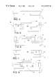
- FIG. 1is a perspective view, partially cut away, of a field effect transistor (FET) formed on silicon substrate with a perforated buried oxide layer in accordance with this invention.
- FETfield effect transistor
- FIG. 2is a cross sectional view of a first step in the fabrication of the FET of this invention.
- FIG. 3is a cross sectional view of a second step in the fabrication of the FET of this invention.
- FIG. 4is a cross sectional view of a third step in the fabrication of the FET of this invention.
- FIG. 5is a cross sectional view of a fourth step in the fabrication of the FET of this invention.
- FIG. 6is a cross sectional view of a fifth step in the fabrication of the FET of this invention.
- FIG. 7is a cross sectional view of a sixth step in the fabrication of the FET of this invention.
- FIG. 8is a cross sectional view of a seventh and eighth steps in the fabrication of the FET of this invention.
- an active region 48 of a field effect transistor 10 of this inventionincludes a channel region 26 , a source region 28 , and a drain region 30 .
- the channel region 26is preferably P-conductivity silicon while the source region 28 and the drain region 30 are each N-conductivity silicon to form two semiconductor junctions 40 and 42 .
- the channel region 26may be N-conductivity silicon while each of the source region 28 and the drain region 30 are P-conductivity silicon.
- the active regionis isolated by an insulating trench 32 which extends from the surface 38 to a perforated buried oxide layer 20 .
- the insulating trench 32has side walls 16 which define the perimeter 22 of the active region 48 and insulates the active region 48 from other structures formed in the silicon substrate 12 .
- the perforated buried oxide layer 20forms the bottom surface 24 of the active region 48 and includes perforated region 36 wherein semi-conductive silicon electrically couples the channel region 26 of the active region 48 to the bulk silicon substrate 12 .
- the channel region 26 potentialwill always remain at the potential of the silicon substrate 12 and can not accumulate a charge, or float, based on historical operation of the FET 10 . It should also be appreciated that because the cross sectional area of the perforated region 36 is significantly smaller than the cross sectional area of the active region 48 , there is no semiconductor junction, or minimal sized semiconductor junction, between either the source region 28 or the drain region 30 and the silicon substrate 12 thereby reducing junction capacitance.
- the first step in the fabrication of the FET 10 of this inventionis to fabricate a silicon on insulator wafer with a perforated buried oxide layer.
- a photoresist mask 18is formed on the surface of the wafer above perforation region 36 to define perforated region 36 .
- a UV sensitive photoresist layer 14is applied to the top surface of the silicon substrate 12 a shown in FIG. 2 .
- Conventional photolithography techniquesare used to pattern the mask 18 and develop the photoresist.
- a UV light source 44 and reticle 34provide collimated light used to expose and pattern the photoresist layer 14 in order to form the mask 18 .
- a developer solutionhardens the photoresist in the unexposed area (e.g. the photoresist mask 18 ) and the UV light dissolves and the developer washes away the photoresist in the exposed area as shown in FIG. 3 .
- SIMOXSeparation by Implantation of Oxygen
- An ION beamis used to implant a high dose of oxygen, greater than 10 E16 atoms per square centimeter, into the silicon substrate.
- the dose and beam energy parameters of the SIMOX processare controlled to control a resultant gaussian concentration of oxygen implanted in the wafer as a function of depth below the surface.
- the dose and beam energyare selected such that the highest concentration of implanted oxygen (e.g. the peak of the gaussian distribution) is at the desired depth of the perforated buried oxide layer 20 and lower concentrations exist both above and below the high concentration layer.
- a heat treatmentthen bonds the implanted oxygen with the silicon to form silicon dioxide (e.g. the high concentration layer becomes the buried oxide layer). Because the photoresist mask 18 blocks the ION beam and thus blocks the implantation of oxygen in the area of the substrate covered by the photoresist mask 18 the masked portion becomes the perforated region 36 after the buried oxide layer is formed in the unmasked region as shown in FIG. 3 .
- the perforated region 36is a region of unoxidized silicon that electrically couples the unoxidized silicon substrate above the buried oxide layer 20 with the unoxidized silicon substrate below the buried oxide layer 20 .
- the photoresist mask 18is removed resulting in silicon on insulator wafer including a silicon substrate 12 with a perforated buried oxide layer 20 as shown in FIG. 4 .
- a thin layer of oxide approximately 150-200 Angstroms thick(not shown) is formed on the top surface of the silicon substrate 12 and a silicon nitride mask 54 is formed thereon.
- the mask 54covers and protects the substrate in the area where the active region 48 of FET 10 is to be formed while leaving the area where the insulating trench 32 is to be formed exposed as shown in FIG. 5 .
- the silicon nitride mask 54is formed by depositing a layer of silicon nitride, approximate 1,500-2,000 Angstroms thick, on the top surface of the oxide and patterning and etching the silicon nitride using conventional photolithography techniques wherein 1) a layer of a UV sensitive photoresist compound is applied to the surface of the silicon nitride; 2) a UV light source and a reticle provide collimated illumination used to expose and pattern the photoresist; 3) a developer solution hardens the unexposed areas of the photoresist while the UV light dissolves the photoresist and the developer washes it away in the exposed portions thereby leaving the unexposed portions as a mask on the surface of the silicon nitride; and 4) a dry etch with an etching compound that etches silicon nitride while not etching the photoresist removes the silicon nitride layer in the areas that are not masked with the photoresist thereby creating the silicon nit
- the unmasked portions of the silicon substrate 12are etched away to form an open trench 56 (approximate 3,000-5,000 Angstrom deep) as shown in FIG. 6 .
- the step of etching the open trench 56may be combined with the step of etching the silicon nitride mask 54 from step four and different etching chemistry will be used for etch of each of the silicon nitride 54 , oxide, and silicon substrate 12 . Because the open trench 56 will later be filled with silicon dioxide to become the insulating trench 32 described in the discussion of FIG.
- the depth of the open trench 56needs to extend at least past the upper surface of the perforated buried oxide layer 20 .
- the etching process for the silicon substrateis typically an anisotropic dry etch using hydrogen bromide (HBr) which has selectivity characteristics such that it etches the silicon substrate 12 but not the silicon nitride mask 54 .
- HBrhydrogen bromide
- the open trench 56is filled with silicon dioxide to form insulating trench 32 .
- Filling the open trench 56preferably uses any known technique for forming silicon dioxide in an open trench such as filling the trench with SiH4 or TEOS and subsequently oxidizing either of such compounds to form insulating silicon dioxide.
- the surface of the waferis polished using a chemical mechanical polish to remove any excess silicon dioxide layer and the remaining silicon nitride mask as shown in FIG. 7 .
- a gate oxide layer 50 , and a polysilicon gate 52are formed on the top surface of the substrate 12 to define the channel region 26 in a conventional CMOS self aligned gate, source, and drain process.
- the gate oxide layer 50is typically grown on the surface of the active region 48 using a thermal oxidation process and a polysilicon layer is deposited on top of the gate oxide layer 50 using a low pressure chemical vapor deposition (LPCVD) process.
- LPCVDlow pressure chemical vapor deposition
- the polysilicon layeris then patterned and etched using the photolithography method discussed earlier to create polysilicon gate 52 which defines the channel region of the FET 10 of this invention as shown in FIG. 8 .
- the portions of the silicon substrate silicon on opposing sides of the P-type silicon in the channel region of the FET 10 that are not masked by the gate applied in the 7 th stepare doped into N-type silicon.
- Dopingis typically performed using Ion implantation techniques. Ions of an N-type dopant 54 , such as arsenic are accelerated to a high velocity in an electric field and impinge on the target wafer. Because the ions cannot penetrate the poly-silicon gate, the poly-silicon gate effectively operates as a mask which results in doping only the exposed source region and drain region as shown in FIG. 8 .
- the foregoing processes of fabricating a field effect transistor on a silicon on insulator wafer with a perforated buried oxide layerresults in a unique transistor structure that eliminates the floating body effect found in known SOI FET structures.
- the perforated regions of the buried oxide layerelectrically couple the channel region of the FET to the silicon substrate to prevent the potential of the channel region from floating based on historical operation of the FET.
- the cross sectional area of the perforated regionspreferably is smaller than the cross sectional area of the channel region to reduce or eliminate junction capacitance problems associated with known CMOS FETs.
Landscapes
- Engineering & Computer Science (AREA)
- Physics & Mathematics (AREA)
- Microelectronics & Electronic Packaging (AREA)
- Condensed Matter Physics & Semiconductors (AREA)
- General Physics & Mathematics (AREA)
- Manufacturing & Machinery (AREA)
- Computer Hardware Design (AREA)
- High Energy & Nuclear Physics (AREA)
- Power Engineering (AREA)
- Toxicology (AREA)
- Health & Medical Sciences (AREA)
- Thin Film Transistor (AREA)
- Element Separation (AREA)
Abstract
Description
Claims (12)
Priority Applications (2)
| Application Number | Priority Date | Filing Date | Title |
|---|---|---|---|
| US09/420,972US6229187B1 (en) | 1999-10-20 | 1999-10-20 | Field effect transistor with non-floating body and method for forming same on a bulk silicon wafer |
| US09/633,960US6465852B1 (en) | 1999-10-20 | 2000-08-08 | Silicon wafer including both bulk and SOI regions and method for forming same on a bulk silicon wafer |
Applications Claiming Priority (1)
| Application Number | Priority Date | Filing Date | Title |
|---|---|---|---|
| US09/420,972US6229187B1 (en) | 1999-10-20 | 1999-10-20 | Field effect transistor with non-floating body and method for forming same on a bulk silicon wafer |
Related Child Applications (1)
| Application Number | Title | Priority Date | Filing Date |
|---|---|---|---|
| US09/633,960Continuation-In-PartUS6465852B1 (en) | 1999-10-20 | 2000-08-08 | Silicon wafer including both bulk and SOI regions and method for forming same on a bulk silicon wafer |
Publications (1)
| Publication Number | Publication Date |
|---|---|
| US6229187B1true US6229187B1 (en) | 2001-05-08 |
Family
ID=23668650
Family Applications (1)
| Application Number | Title | Priority Date | Filing Date |
|---|---|---|---|
| US09/420,972Expired - LifetimeUS6229187B1 (en) | 1999-10-20 | 1999-10-20 | Field effect transistor with non-floating body and method for forming same on a bulk silicon wafer |
Country Status (1)
| Country | Link |
|---|---|
| US (1) | US6229187B1 (en) |
Cited By (20)
| Publication number | Priority date | Publication date | Assignee | Title |
|---|---|---|---|---|
| US20030008438A1 (en)* | 2000-11-15 | 2003-01-09 | Abbott Todd R. | Method of forming a field effect transistor |
| US6514809B1 (en)* | 2000-11-03 | 2003-02-04 | Advanced Micro Devices, Inc. | SOI field effect transistors with body contacts formed by selective etch and fill |
| US6680650B2 (en) | 2001-01-12 | 2004-01-20 | Broadcom Corporation | MOSFET well biasing scheme that migrates body effect |
| US20040033646A1 (en)* | 2002-08-15 | 2004-02-19 | Tang Sanh D. | Methods of forming field effect transistors, and methods of forming integrated circuitry |
| US6828202B1 (en) | 2002-10-01 | 2004-12-07 | T-Ram, Inc. | Semiconductor region self-aligned with ion implant shadowing |
| US20050164468A1 (en)* | 2003-06-26 | 2005-07-28 | Steegen An L. | Selective silicon-on-insulator isolation structure and method |
| US20060131689A1 (en)* | 2004-12-17 | 2006-06-22 | Fujitsu Limited | Semiconductor device and fabrication method thereof |
| US20080108184A1 (en)* | 2003-12-02 | 2008-05-08 | International Business Machines Corporation | Planar substrate with selected semiconductor crystal orientations formed by localized amorphization and recrystallization of stacked template layers |
| US20080150074A1 (en)* | 2006-12-21 | 2008-06-26 | Chartered Semiconductor Manufacturing Ltd. | Integrated circuit system with isolation |
| US20110012669A1 (en)* | 2009-07-15 | 2011-01-20 | Io Semiconductor, Inc. | Semiconductor-on-insulator with back side connection |
| US8912646B2 (en) | 2009-07-15 | 2014-12-16 | Silanna Semiconductor U.S.A., Inc. | Integrated circuit assembly and method of making |
| US9203396B1 (en) | 2013-02-22 | 2015-12-01 | Triquint Semiconductor, Inc. | Radio frequency switch device with source-follower |
| US9214932B2 (en) | 2013-02-11 | 2015-12-15 | Triquint Semiconductor, Inc. | Body-biased switching device |
| US9379698B2 (en) | 2014-02-04 | 2016-06-28 | Triquint Semiconductor, Inc. | Field effect transistor switching circuit |
| US9390974B2 (en) | 2012-12-21 | 2016-07-12 | Qualcomm Incorporated | Back-to-back stacked integrated circuit assembly and method of making |
| US9466719B2 (en) | 2009-07-15 | 2016-10-11 | Qualcomm Incorporated | Semiconductor-on-insulator with back side strain topology |
| US9496227B2 (en) | 2009-07-15 | 2016-11-15 | Qualcomm Incorporated | Semiconductor-on-insulator with back side support layer |
| US9515181B2 (en) | 2014-08-06 | 2016-12-06 | Qualcomm Incorporated | Semiconductor device with self-aligned back side features |
| US9748272B2 (en) | 2009-07-15 | 2017-08-29 | Qualcomm Incorporated | Semiconductor-on-insulator with back side strain inducing material |
| US10515801B2 (en) | 2007-06-04 | 2019-12-24 | Micron Technology, Inc. | Pitch multiplication using self-assembling materials |
Citations (30)
| Publication number | Priority date | Publication date | Assignee | Title |
|---|---|---|---|---|
| US4682407A (en) | 1986-01-21 | 1987-07-28 | Motorola, Inc. | Means and method for stabilizing polycrystalline semiconductor layers |
| US4888300A (en) | 1985-11-07 | 1989-12-19 | Fairchild Camera And Instrument Corporation | Submerged wall isolation of silicon islands |
| EP0480373A2 (en) | 1990-10-09 | 1992-04-15 | Seiko Epson Corporation | Thin-film semiconductor device |
| US5262346A (en) | 1992-12-16 | 1993-11-16 | International Business Machines Corporation | Nitride polish stop for forming SOI wafers |
| US5391503A (en) | 1991-05-13 | 1995-02-21 | Sony Corporation | Method of forming a stacked semiconductor device wherein semiconductor layers and insulating films are sequentially stacked and forming openings through such films and etchings using one of the insulating films as a mask |
| US5401998A (en) | 1992-12-03 | 1995-03-28 | Chiu; Kuang Y. | Trench isolation using doped sidewalls |
| US5466630A (en) | 1994-03-21 | 1995-11-14 | United Microelectronics Corp. | Silicon-on-insulator technique with buried gap |
| US5489792A (en) | 1994-04-07 | 1996-02-06 | Regents Of The University Of California | Silicon-on-insulator transistors having improved current characteristics and reduced electrostatic discharge susceptibility |
| US5494837A (en)* | 1994-09-27 | 1996-02-27 | Purdue Research Foundation | Method of forming semiconductor-on-insulator electronic devices by growing monocrystalline semiconducting regions from trench sidewalls |
| US5543338A (en) | 1992-07-08 | 1996-08-06 | Rohm Co., Ltd | Method for manufacturing a semiconductor device using a semiconductor-on-insulator substrate |
| US5618345A (en) | 1994-03-18 | 1997-04-08 | Agency Of Industrial Science & Technology, Ministry Of International Trade & Industry | Method of producing self-supporting thin film of silicon single crystal |
| US5620912A (en) | 1994-07-21 | 1997-04-15 | Lg Semicon Co., Ltd. | Method of manufacturing a semiconductor device using a spacer |
| US5674760A (en)* | 1996-02-26 | 1997-10-07 | United Microelectronics Corporation | Method of forming isolation regions in a MOS transistor device |
| US5683932A (en) | 1994-03-15 | 1997-11-04 | National Semiconductor Corporation | Method of fabricating a planarized trench and field oxide isolation structure |
| US5702989A (en) | 1996-02-08 | 1997-12-30 | Taiwan Semiconductor Manufacturing Company Ltd. | Method for fabricating a tub structured stacked capacitor for a DRAM cell having a central column |
| US5804856A (en) | 1996-11-27 | 1998-09-08 | Advanced Mirco Devices, Inc. | Depleted sidewall-poly LDD transistor |
| US5811855A (en) | 1997-12-29 | 1998-09-22 | United Technologies Corporation | SOI combination body tie |
| US5811588A (en) | 1994-10-17 | 1998-09-22 | Dsm N.V. | Process for the preparation of 3-phenylpropanal |
| US5825696A (en) | 1993-12-03 | 1998-10-20 | Mitsubishi Denki Kabushiki Kaisha | Semiconductor memory device including an SOI substrate |
| US5846857A (en) | 1997-09-05 | 1998-12-08 | Advanced Micro Devices, Inc. | CMOS processing employing removable sidewall spacers for independently optimized N- and P-channel transistor performance |
| US5877046A (en) | 1996-04-09 | 1999-03-02 | Samsung Electronics Co., Ltd. | Methods of forming semiconductor-on-insulator substrates |
| US5879975A (en) | 1997-09-05 | 1999-03-09 | Advanced Micro Devices, Inc. | Heat treating nitrogen implanted gate electrode layer for improved gate electrode etch profile |
| US5894152A (en) | 1997-06-18 | 1999-04-13 | International Business Machines Corporation | SOI/bulk hybrid substrate and method of forming the same |
| US5907768A (en) | 1996-08-16 | 1999-05-25 | Kobe Steel Usa Inc. | Methods for fabricating microelectronic structures including semiconductor islands |
| US5972758A (en) | 1997-12-04 | 1999-10-26 | Intel Corporation | Pedestal isolated junction structure and method of manufacture |
| US5976945A (en) | 1997-11-20 | 1999-11-02 | Vanguard International Semiconductor Corporation | Method for fabricating a DRAM cell structure on an SOI wafer incorporating a two dimensional trench capacitor |
| US5977579A (en) | 1998-12-03 | 1999-11-02 | Micron Technology, Inc. | Trench dram cell with vertical device and buried word lines |
| US6004864A (en) | 1998-02-25 | 1999-12-21 | Taiwan Semiconductor Manufacturing Company Ltd. | Ion implant method for forming trench isolation for integrated circuit devices |
| US6008104A (en) | 1998-04-06 | 1999-12-28 | Siemens Aktiengesellschaft | Method of fabricating a trench capacitor with a deposited isolation collar |
| US6066527A (en) | 1999-07-26 | 2000-05-23 | Infineon Technologies North America Corp. | Buried strap poly etch back (BSPE) process |
- 1999
- 1999-10-20USUS09/420,972patent/US6229187B1/ennot_activeExpired - Lifetime
Patent Citations (30)
| Publication number | Priority date | Publication date | Assignee | Title |
|---|---|---|---|---|
| US4888300A (en) | 1985-11-07 | 1989-12-19 | Fairchild Camera And Instrument Corporation | Submerged wall isolation of silicon islands |
| US4682407A (en) | 1986-01-21 | 1987-07-28 | Motorola, Inc. | Means and method for stabilizing polycrystalline semiconductor layers |
| EP0480373A2 (en) | 1990-10-09 | 1992-04-15 | Seiko Epson Corporation | Thin-film semiconductor device |
| US5391503A (en) | 1991-05-13 | 1995-02-21 | Sony Corporation | Method of forming a stacked semiconductor device wherein semiconductor layers and insulating films are sequentially stacked and forming openings through such films and etchings using one of the insulating films as a mask |
| US5543338A (en) | 1992-07-08 | 1996-08-06 | Rohm Co., Ltd | Method for manufacturing a semiconductor device using a semiconductor-on-insulator substrate |
| US5401998A (en) | 1992-12-03 | 1995-03-28 | Chiu; Kuang Y. | Trench isolation using doped sidewalls |
| US5262346A (en) | 1992-12-16 | 1993-11-16 | International Business Machines Corporation | Nitride polish stop for forming SOI wafers |
| US5825696A (en) | 1993-12-03 | 1998-10-20 | Mitsubishi Denki Kabushiki Kaisha | Semiconductor memory device including an SOI substrate |
| US5683932A (en) | 1994-03-15 | 1997-11-04 | National Semiconductor Corporation | Method of fabricating a planarized trench and field oxide isolation structure |
| US5618345A (en) | 1994-03-18 | 1997-04-08 | Agency Of Industrial Science & Technology, Ministry Of International Trade & Industry | Method of producing self-supporting thin film of silicon single crystal |
| US5466630A (en) | 1994-03-21 | 1995-11-14 | United Microelectronics Corp. | Silicon-on-insulator technique with buried gap |
| US5489792A (en) | 1994-04-07 | 1996-02-06 | Regents Of The University Of California | Silicon-on-insulator transistors having improved current characteristics and reduced electrostatic discharge susceptibility |
| US5620912A (en) | 1994-07-21 | 1997-04-15 | Lg Semicon Co., Ltd. | Method of manufacturing a semiconductor device using a spacer |
| US5494837A (en)* | 1994-09-27 | 1996-02-27 | Purdue Research Foundation | Method of forming semiconductor-on-insulator electronic devices by growing monocrystalline semiconducting regions from trench sidewalls |
| US5811588A (en) | 1994-10-17 | 1998-09-22 | Dsm N.V. | Process for the preparation of 3-phenylpropanal |
| US5702989A (en) | 1996-02-08 | 1997-12-30 | Taiwan Semiconductor Manufacturing Company Ltd. | Method for fabricating a tub structured stacked capacitor for a DRAM cell having a central column |
| US5674760A (en)* | 1996-02-26 | 1997-10-07 | United Microelectronics Corporation | Method of forming isolation regions in a MOS transistor device |
| US5877046A (en) | 1996-04-09 | 1999-03-02 | Samsung Electronics Co., Ltd. | Methods of forming semiconductor-on-insulator substrates |
| US5907768A (en) | 1996-08-16 | 1999-05-25 | Kobe Steel Usa Inc. | Methods for fabricating microelectronic structures including semiconductor islands |
| US5804856A (en) | 1996-11-27 | 1998-09-08 | Advanced Mirco Devices, Inc. | Depleted sidewall-poly LDD transistor |
| US5894152A (en) | 1997-06-18 | 1999-04-13 | International Business Machines Corporation | SOI/bulk hybrid substrate and method of forming the same |
| US5846857A (en) | 1997-09-05 | 1998-12-08 | Advanced Micro Devices, Inc. | CMOS processing employing removable sidewall spacers for independently optimized N- and P-channel transistor performance |
| US5879975A (en) | 1997-09-05 | 1999-03-09 | Advanced Micro Devices, Inc. | Heat treating nitrogen implanted gate electrode layer for improved gate electrode etch profile |
| US5976945A (en) | 1997-11-20 | 1999-11-02 | Vanguard International Semiconductor Corporation | Method for fabricating a DRAM cell structure on an SOI wafer incorporating a two dimensional trench capacitor |
| US5972758A (en) | 1997-12-04 | 1999-10-26 | Intel Corporation | Pedestal isolated junction structure and method of manufacture |
| US5811855A (en) | 1997-12-29 | 1998-09-22 | United Technologies Corporation | SOI combination body tie |
| US6004864A (en) | 1998-02-25 | 1999-12-21 | Taiwan Semiconductor Manufacturing Company Ltd. | Ion implant method for forming trench isolation for integrated circuit devices |
| US6008104A (en) | 1998-04-06 | 1999-12-28 | Siemens Aktiengesellschaft | Method of fabricating a trench capacitor with a deposited isolation collar |
| US5977579A (en) | 1998-12-03 | 1999-11-02 | Micron Technology, Inc. | Trench dram cell with vertical device and buried word lines |
| US6066527A (en) | 1999-07-26 | 2000-05-23 | Infineon Technologies North America Corp. | Buried strap poly etch back (BSPE) process |
Non-Patent Citations (1)
| Title |
|---|
| S. Wolf and R.N. Tauber, Silicon Processing for the VLSI ERA, vol. 1, p. 531. |
Cited By (55)
| Publication number | Priority date | Publication date | Assignee | Title |
|---|---|---|---|---|
| US6514809B1 (en)* | 2000-11-03 | 2003-02-04 | Advanced Micro Devices, Inc. | SOI field effect transistors with body contacts formed by selective etch and fill |
| US20030015766A1 (en)* | 2000-11-15 | 2003-01-23 | Abbott Todd R. | Integrated circuitry |
| US20030008438A1 (en)* | 2000-11-15 | 2003-01-09 | Abbott Todd R. | Method of forming a field effect transistor |
| US7153731B2 (en) | 2000-11-15 | 2006-12-26 | Micron Technology, Inc. | Method of forming a field effect transistor with halo implant regions |
| US20050003627A1 (en)* | 2000-11-15 | 2005-01-06 | Abbott Todd R. | Method of forming a field effect transistor |
| US7112482B2 (en) | 2000-11-15 | 2006-09-26 | Micron Technology, Inc. | Method of forming a field effect transistor |
| US6987291B2 (en) | 2000-11-15 | 2006-01-17 | Micron Technology, Inc. | Integrated transistor circuitry |
| US6956434B2 (en) | 2001-01-12 | 2005-10-18 | Broadcom Corporation | MOSFET well biasing scheme that mitigates body effect |
| US6680650B2 (en) | 2001-01-12 | 2004-01-20 | Broadcom Corporation | MOSFET well biasing scheme that migrates body effect |
| US7019591B2 (en) | 2001-01-12 | 2006-03-28 | Broadcom Corporation | Gain boosted operational amplifier having a field effect transistor with a well biasing scheme |
| US20050264357A1 (en)* | 2001-01-12 | 2005-12-01 | Broadcom Corporation | Gain boosted operational amplifier having a field effect transistor with a well biasing scheme |
| US20050095767A1 (en)* | 2002-08-15 | 2005-05-05 | Tang Sanh D. | Methods of forming field effect transistors and methods of forming field effect transistor gates and gate lines |
| US7118950B2 (en) | 2002-08-15 | 2006-10-10 | Micron Technology, Inc. | Method of forming a field effect transistor |
| US7470576B2 (en) | 2002-08-15 | 2008-12-30 | Micron Technology, Inc. | Methods of forming field effect transistor gate lines |
| US20050106795A1 (en)* | 2002-08-15 | 2005-05-19 | Tang Sanh D. | Methods of forming field effect transistors and methods of forming field effect transistor gates and gate lines |
| US20050101075A1 (en)* | 2002-08-15 | 2005-05-12 | Tang Sanh D. | Method of forming a field effect transistors |
| US20050095756A1 (en)* | 2002-08-15 | 2005-05-05 | Tang Sanh D. | Method of forming a field effect transistor |
| US8802520B2 (en) | 2002-08-15 | 2014-08-12 | Micron Technology, Inc. | Method of forming a field effect transistor having source/drain material over insulative material |
| US7071043B2 (en) | 2002-08-15 | 2006-07-04 | Micron Technology, Inc. | Methods of forming a field effect transistor having source/drain material over insulative material |
| US20080311719A1 (en)* | 2002-08-15 | 2008-12-18 | Tang Sanh D | Method Of Forming A Field Effect Transistor |
| US6936507B2 (en) | 2002-08-15 | 2005-08-30 | Micron Technology, Inc. | Method of forming field effect transistors |
| US20060258107A1 (en)* | 2002-08-15 | 2006-11-16 | Tang Sanh D | Methods of forming field effect transistors and methods of forming field effect transistor gates and gate lines |
| US7465616B2 (en) | 2002-08-15 | 2008-12-16 | Micron Technology, Inc. | Method of forming a field effect transistor |
| US20070105323A1 (en)* | 2002-08-15 | 2007-05-10 | Tang Sanh D | Method of forming a field effect transistor |
| US8440515B2 (en) | 2002-08-15 | 2013-05-14 | Micron Technology, Inc. | Method of forming a field effect transistor |
| US20040033646A1 (en)* | 2002-08-15 | 2004-02-19 | Tang Sanh D. | Methods of forming field effect transistors, and methods of forming integrated circuitry |
| US6828202B1 (en) | 2002-10-01 | 2004-12-07 | T-Ram, Inc. | Semiconductor region self-aligned with ion implant shadowing |
| US20080029818A1 (en)* | 2003-06-26 | 2008-02-07 | Steegen An L | Selective silicon-on-insulator isolation structure and method |
| US7326983B2 (en)* | 2003-06-26 | 2008-02-05 | International Business Machines Corporation | Selective silicon-on-insulator isolation structure and method |
| US7923786B2 (en) | 2003-06-26 | 2011-04-12 | International Business Machines Corporation | Selective silicon-on-insulator isolation structure and method |
| US20050164468A1 (en)* | 2003-06-26 | 2005-07-28 | Steegen An L. | Selective silicon-on-insulator isolation structure and method |
| US20080108184A1 (en)* | 2003-12-02 | 2008-05-08 | International Business Machines Corporation | Planar substrate with selected semiconductor crystal orientations formed by localized amorphization and recrystallization of stacked template layers |
| US7785939B2 (en)* | 2003-12-02 | 2010-08-31 | International Business Machines Corporation | Planar substrate with selected semiconductor crystal orientations formed by localized amorphization and recrystallization of stacked template layers |
| US20060131689A1 (en)* | 2004-12-17 | 2006-06-22 | Fujitsu Limited | Semiconductor device and fabrication method thereof |
| US20080150074A1 (en)* | 2006-12-21 | 2008-06-26 | Chartered Semiconductor Manufacturing Ltd. | Integrated circuit system with isolation |
| US8053327B2 (en)* | 2006-12-21 | 2011-11-08 | Globalfoundries Singapore Pte. Ltd. | Method of manufacture of an integrated circuit system with self-aligned isolation structures |
| US10515801B2 (en) | 2007-06-04 | 2019-12-24 | Micron Technology, Inc. | Pitch multiplication using self-assembling materials |
| US9412644B2 (en) | 2009-07-15 | 2016-08-09 | Qualcomm Incorporated | Integrated circuit assembly and method of making |
| US9368468B2 (en) | 2009-07-15 | 2016-06-14 | Qualcomm Switch Corp. | Thin integrated circuit chip-on-board assembly |
| US8859347B2 (en) | 2009-07-15 | 2014-10-14 | Silanna Semiconductor U.S.A., Inc. | Semiconductor-on-insulator with back side body connection |
| US8912646B2 (en) | 2009-07-15 | 2014-12-16 | Silanna Semiconductor U.S.A., Inc. | Integrated circuit assembly and method of making |
| US8921168B2 (en) | 2009-07-15 | 2014-12-30 | Silanna Semiconductor U.S.A., Inc. | Thin integrated circuit chip-on-board assembly and method of making |
| US8357975B2 (en) | 2009-07-15 | 2013-01-22 | Io Semiconductor, Inc. | Semiconductor-on-insulator with back side connection |
| US10217822B2 (en) | 2009-07-15 | 2019-02-26 | Qualcomm Incorporated | Semiconductor-on-insulator with back side heat dissipation |
| US9748272B2 (en) | 2009-07-15 | 2017-08-29 | Qualcomm Incorporated | Semiconductor-on-insulator with back side strain inducing material |
| US8232597B2 (en) | 2009-07-15 | 2012-07-31 | Io Semiconductor, Inc. | Semiconductor-on-insulator with back side connection |
| US9496227B2 (en) | 2009-07-15 | 2016-11-15 | Qualcomm Incorporated | Semiconductor-on-insulator with back side support layer |
| US20110012669A1 (en)* | 2009-07-15 | 2011-01-20 | Io Semiconductor, Inc. | Semiconductor-on-insulator with back side connection |
| US9466719B2 (en) | 2009-07-15 | 2016-10-11 | Qualcomm Incorporated | Semiconductor-on-insulator with back side strain topology |
| US9390974B2 (en) | 2012-12-21 | 2016-07-12 | Qualcomm Incorporated | Back-to-back stacked integrated circuit assembly and method of making |
| US9576937B2 (en) | 2012-12-21 | 2017-02-21 | Qualcomm Incorporated | Back-to-back stacked integrated circuit assembly |
| US9214932B2 (en) | 2013-02-11 | 2015-12-15 | Triquint Semiconductor, Inc. | Body-biased switching device |
| US9203396B1 (en) | 2013-02-22 | 2015-12-01 | Triquint Semiconductor, Inc. | Radio frequency switch device with source-follower |
| US9379698B2 (en) | 2014-02-04 | 2016-06-28 | Triquint Semiconductor, Inc. | Field effect transistor switching circuit |
| US9515181B2 (en) | 2014-08-06 | 2016-12-06 | Qualcomm Incorporated | Semiconductor device with self-aligned back side features |
Similar Documents
| Publication | Publication Date | Title |
|---|---|---|
| US6229187B1 (en) | Field effect transistor with non-floating body and method for forming same on a bulk silicon wafer | |
| US6376286B1 (en) | Field effect transistor with non-floating body and method for forming same on a bulk silicon wafer | |
| US6611023B1 (en) | Field effect transistor with self alligned double gate and method of forming same | |
| US6566176B1 (en) | SOI device with wrap-around contact to underside of body, and method of making | |
| US6548859B2 (en) | MOS semiconductor device and method of manufacturing the same | |
| US5166084A (en) | Process for fabricating a silicon on insulator field effect transistor | |
| US6153476A (en) | Semiconductor device and method for manufacturing the same | |
| US6465852B1 (en) | Silicon wafer including both bulk and SOI regions and method for forming same on a bulk silicon wafer | |
| KR100265081B1 (en) | Memory cell and method for fabricating the same | |
| KR100615125B1 (en) | Semiconductor devices | |
| US20020111025A1 (en) | Modified gate processing for optimized difinition of array and logic devices on same chip | |
| US5310692A (en) | Method of forming a MOSFET structure with planar surface | |
| US5930614A (en) | Method for forming MOS device having field shield isolation | |
| KR20030050995A (en) | Method for fabricating high-integrated transistor | |
| KR100422412B1 (en) | Cylindrical type transistor having vertical silicon-on-insulator structure and fabrication method thereof | |
| US6534822B1 (en) | Silicon on insulator field effect transistor with a double Schottky gate structure | |
| KR19990002942A (en) | Manufacturing method of SOI device | |
| US6255147B1 (en) | Silicon on insulator circuit structure with extra narrow field transistors and method of forming same | |
| KR100406500B1 (en) | Method for fabricating semiconductor device | |
| US7030020B2 (en) | Method to shrink cell size in a split gate flash | |
| KR100234728B1 (en) | MOS field effect transistor manufacturing method | |
| JP2734434B2 (en) | Semiconductor device and manufacturing method thereof | |
| KR100533167B1 (en) | Method of manufacturing for semiconductor and the same | |
| KR960015524B1 (en) | Semiconductor memory device and the manufacturing method | |
| KR0165306B1 (en) | Semiconductor memory device & its fabrication method |
Legal Events
| Date | Code | Title | Description |
|---|---|---|---|
| AS | Assignment | Owner name:ADVANCED MICRO DEVICES, INC., CALIFORNIA Free format text:ASSIGNMENT OF ASSIGNORS INTEREST;ASSIGNOR:JU, DONG-HYUK;REEL/FRAME:010344/0159 Effective date:19991015 | |
| STCF | Information on status: patent grant | Free format text:PATENTED CASE | |
| FPAY | Fee payment | Year of fee payment:4 | |
| FPAY | Fee payment | Year of fee payment:8 | |
| AS | Assignment | Owner name:GLOBALFOUNDRIES INC., CAYMAN ISLANDS Free format text:AFFIRMATION OF PATENT ASSIGNMENT;ASSIGNOR:ADVANCED MICRO DEVICES, INC.;REEL/FRAME:023119/0083 Effective date:20090630 | |
| FPAY | Fee payment | Year of fee payment:12 | |
| AS | Assignment | Owner name:WILMINGTON TRUST, NATIONAL ASSOCIATION, DELAWARE Free format text:SECURITY AGREEMENT;ASSIGNOR:GLOBALFOUNDRIES INC.;REEL/FRAME:049490/0001 Effective date:20181127 | |
| AS | Assignment | Owner name:GLOBALFOUNDRIES INC., CAYMAN ISLANDS Free format text:RELEASE BY SECURED PARTY;ASSIGNOR:WILMINGTON TRUST, NATIONAL ASSOCIATION;REEL/FRAME:054636/0001 Effective date:20201117 | |
| AS | Assignment | Owner name:GLOBALFOUNDRIES U.S. INC., NEW YORK Free format text:RELEASE BY SECURED PARTY;ASSIGNOR:WILMINGTON TRUST, NATIONAL ASSOCIATION;REEL/FRAME:056987/0001 Effective date:20201117 |