US6228773B1 - Synchronous multiplexed near zero overhead architecture for vacuum processes - Google Patents
Synchronous multiplexed near zero overhead architecture for vacuum processesDownload PDFInfo
- Publication number
- US6228773B1 US6228773B1US09/060,095US6009598AUS6228773B1US 6228773 B1US6228773 B1US 6228773B1US 6009598 AUS6009598 AUS 6009598AUS 6228773 B1US6228773 B1US 6228773B1
- Authority
- US
- United States
- Prior art keywords
- chamber
- processing
- workpiece
- plasma
- steps
- Prior art date
- Legal status (The legal status is an assumption and is not a legal conclusion. Google has not performed a legal analysis and makes no representation as to the accuracy of the status listed.)
- Expired - Lifetime
Links
- 238000000034methodMethods0.000titleclaimsdescription146
- 230000008569processEffects0.000titleclaimsdescription96
- 230000001360synchronised effectEffects0.000titledescription4
- 238000012545processingMethods0.000claimsabstractdescription167
- 230000009977dual effectEffects0.000claimsabstractdescription33
- 238000005086pumpingMethods0.000claimsabstractdescription14
- 230000000087stabilizing effectEffects0.000claimsabstract2
- 239000007789gasSubstances0.000claimsdescription43
- 238000013022ventingMethods0.000claimsdescription21
- 229920002120photoresistant polymerPolymers0.000claimsdescription17
- 238000004380ashingMethods0.000claimsdescription8
- 238000005530etchingMethods0.000claimsdescription7
- 238000007781pre-processingMethods0.000claimsdescription7
- 238000012805post-processingMethods0.000claimsdescription6
- 238000011437continuous methodMethods0.000claimsdescription5
- 230000003993interactionEffects0.000claimsdescription5
- 239000000758substrateSubstances0.000claimsdescription5
- 230000000903blocking effectEffects0.000claimsdescription4
- 239000000835fiberSubstances0.000claimsdescription3
- 238000011068loading methodMethods0.000claimsdescription3
- 238000004519manufacturing processMethods0.000claimsdescription3
- 230000003287optical effectEffects0.000claimsdescription3
- 238000010926purgeMethods0.000claimsdescription3
- 238000001020plasma etchingMethods0.000claims6
- 238000009832plasma treatmentMethods0.000claims3
- 238000011144upstream manufacturingMethods0.000claims2
- 238000004904shorteningMethods0.000claims1
- 235000012431wafersNutrition0.000abstractdescription122
- 239000004065semiconductorSubstances0.000abstractdescription18
- 210000002381plasmaAnatomy0.000description30
- 238000010586diagramMethods0.000description14
- 238000012546transferMethods0.000description14
- 230000008901benefitEffects0.000description6
- 239000003921oilSubstances0.000description6
- QVGXLLKOCUKJST-UHFFFAOYSA-Natomic oxygenChemical compound[O]QVGXLLKOCUKJST-UHFFFAOYSA-N0.000description5
- 229910052760oxygenInorganic materials0.000description5
- 239000001301oxygenSubstances0.000description5
- 238000009826distributionMethods0.000description4
- 230000007246mechanismEffects0.000description4
- 150000001875compoundsChemical class0.000description3
- 238000000151depositionMethods0.000description3
- 238000002955isolationMethods0.000description3
- 230000009467reductionEffects0.000description3
- 238000004140cleaningMethods0.000description2
- 238000004891communicationMethods0.000description2
- 230000003750conditioning effectEffects0.000description2
- 238000011109contaminationMethods0.000description2
- 238000001816coolingMethods0.000description2
- 230000000694effectsEffects0.000description2
- 238000010438heat treatmentMethods0.000description2
- 238000005461lubricationMethods0.000description2
- 239000000463materialSubstances0.000description2
- 238000012986modificationMethods0.000description2
- 230000004048modificationEffects0.000description2
- 239000002245particleSubstances0.000description2
- 238000002360preparation methodMethods0.000description2
- 238000001228spectrumMethods0.000description2
- 230000006641stabilisationEffects0.000description2
- 238000011105stabilizationMethods0.000description2
- OKTJSMMVPCPJKN-UHFFFAOYSA-NCarbonChemical group[C]OKTJSMMVPCPJKN-UHFFFAOYSA-N0.000description1
- CBENFWSGALASAD-UHFFFAOYSA-NOzoneChemical compound[O-][O+]=OCBENFWSGALASAD-UHFFFAOYSA-N0.000description1
- XUIMIQQOPSSXEZ-UHFFFAOYSA-NSiliconChemical compound[Si]XUIMIQQOPSSXEZ-UHFFFAOYSA-N0.000description1
- 238000000429assemblyMethods0.000description1
- 125000004429atomChemical group0.000description1
- 238000010923batch productionMethods0.000description1
- 239000003990capacitorSubstances0.000description1
- 229910052799carbonInorganic materials0.000description1
- 230000008859changeEffects0.000description1
- 238000012993chemical processingMethods0.000description1
- 238000006243chemical reactionMethods0.000description1
- 239000011248coating agentSubstances0.000description1
- 238000000576coating methodMethods0.000description1
- 230000002860competitive effectEffects0.000description1
- 238000004590computer programMethods0.000description1
- 238000009833condensationMethods0.000description1
- 230000005494condensationEffects0.000description1
- 238000005260corrosionMethods0.000description1
- 230000007797corrosionEffects0.000description1
- 230000008021depositionEffects0.000description1
- 238000003795desorptionMethods0.000description1
- 230000005684electric fieldEffects0.000description1
- 230000008030eliminationEffects0.000description1
- 238000003379elimination reactionMethods0.000description1
- 125000001153fluoro groupChemical groupF*0.000description1
- 230000008570general processEffects0.000description1
- 239000003779heat-resistant materialSubstances0.000description1
- 238000009616inductively coupled plasmaMethods0.000description1
- 150000002500ionsChemical class0.000description1
- 238000005304joiningMethods0.000description1
- 230000001050lubricating effectEffects0.000description1
- 238000005457optimizationMethods0.000description1
- 150000002894organic compoundsChemical class0.000description1
- 230000005855radiationEffects0.000description1
- 238000007789sealingMethods0.000description1
- 238000007493shaping processMethods0.000description1
- 229910052710siliconInorganic materials0.000description1
- 239000010703siliconSubstances0.000description1
- 238000010408sweepingMethods0.000description1
- 239000002341toxic gasSubstances0.000description1
- 239000003039volatile agentSubstances0.000description1
Images


Classifications
- H—ELECTRICITY
- H01—ELECTRIC ELEMENTS
- H01L—SEMICONDUCTOR DEVICES NOT COVERED BY CLASS H10
- H01L21/00—Processes or apparatus adapted for the manufacture or treatment of semiconductor or solid state devices or of parts thereof
- H01L21/02—Manufacture or treatment of semiconductor devices or of parts thereof
- H01L21/04—Manufacture or treatment of semiconductor devices or of parts thereof the devices having potential barriers, e.g. a PN junction, depletion layer or carrier concentration layer
- H01L21/18—Manufacture or treatment of semiconductor devices or of parts thereof the devices having potential barriers, e.g. a PN junction, depletion layer or carrier concentration layer the devices having semiconductor bodies comprising elements of Group IV of the Periodic Table or AIIIBV compounds with or without impurities, e.g. doping materials
- H01L21/30—Treatment of semiconductor bodies using processes or apparatus not provided for in groups H01L21/20 - H01L21/26
- H—ELECTRICITY
- H01—ELECTRIC ELEMENTS
- H01L—SEMICONDUCTOR DEVICES NOT COVERED BY CLASS H10
- H01L21/00—Processes or apparatus adapted for the manufacture or treatment of semiconductor or solid state devices or of parts thereof
- H01L21/67—Apparatus specially adapted for handling semiconductor or electric solid state devices during manufacture or treatment thereof; Apparatus specially adapted for handling wafers during manufacture or treatment of semiconductor or electric solid state devices or components ; Apparatus not specifically provided for elsewhere
- H01L21/67005—Apparatus not specifically provided for elsewhere
- H01L21/67011—Apparatus for manufacture or treatment
- H01L21/67155—Apparatus for manufacturing or treating in a plurality of work-stations
- H01L21/6719—Apparatus for manufacturing or treating in a plurality of work-stations characterized by the construction of the processing chambers, e.g. modular processing chambers
- H—ELECTRICITY
- H01—ELECTRIC ELEMENTS
- H01L—SEMICONDUCTOR DEVICES NOT COVERED BY CLASS H10
- H01L21/00—Processes or apparatus adapted for the manufacture or treatment of semiconductor or solid state devices or of parts thereof
- H01L21/67—Apparatus specially adapted for handling semiconductor or electric solid state devices during manufacture or treatment thereof; Apparatus specially adapted for handling wafers during manufacture or treatment of semiconductor or electric solid state devices or components ; Apparatus not specifically provided for elsewhere
- H01L21/67005—Apparatus not specifically provided for elsewhere
- H01L21/67011—Apparatus for manufacture or treatment
- H01L21/67017—Apparatus for fluid treatment
- H—ELECTRICITY
- H01—ELECTRIC ELEMENTS
- H01L—SEMICONDUCTOR DEVICES NOT COVERED BY CLASS H10
- H01L21/00—Processes or apparatus adapted for the manufacture or treatment of semiconductor or solid state devices or of parts thereof
- H01L21/67—Apparatus specially adapted for handling semiconductor or electric solid state devices during manufacture or treatment thereof; Apparatus specially adapted for handling wafers during manufacture or treatment of semiconductor or electric solid state devices or components ; Apparatus not specifically provided for elsewhere
- H01L21/67005—Apparatus not specifically provided for elsewhere
- H01L21/67011—Apparatus for manufacture or treatment
- H01L21/67155—Apparatus for manufacturing or treating in a plurality of work-stations
- H01L21/67196—Apparatus for manufacturing or treating in a plurality of work-stations characterized by the construction of the transfer chamber
- H—ELECTRICITY
- H01—ELECTRIC ELEMENTS
- H01L—SEMICONDUCTOR DEVICES NOT COVERED BY CLASS H10
- H01L21/00—Processes or apparatus adapted for the manufacture or treatment of semiconductor or solid state devices or of parts thereof
- H01L21/67—Apparatus specially adapted for handling semiconductor or electric solid state devices during manufacture or treatment thereof; Apparatus specially adapted for handling wafers during manufacture or treatment of semiconductor or electric solid state devices or components ; Apparatus not specifically provided for elsewhere
- H01L21/67005—Apparatus not specifically provided for elsewhere
- H01L21/67242—Apparatus for monitoring, sorting or marking
- H01L21/67253—Process monitoring, e.g. flow or thickness monitoring
- H—ELECTRICITY
- H01—ELECTRIC ELEMENTS
- H01L—SEMICONDUCTOR DEVICES NOT COVERED BY CLASS H10
- H01L21/00—Processes or apparatus adapted for the manufacture or treatment of semiconductor or solid state devices or of parts thereof
- H01L21/67—Apparatus specially adapted for handling semiconductor or electric solid state devices during manufacture or treatment thereof; Apparatus specially adapted for handling wafers during manufacture or treatment of semiconductor or electric solid state devices or components ; Apparatus not specifically provided for elsewhere
- H01L21/677—Apparatus specially adapted for handling semiconductor or electric solid state devices during manufacture or treatment thereof; Apparatus specially adapted for handling wafers during manufacture or treatment of semiconductor or electric solid state devices or components ; Apparatus not specifically provided for elsewhere for conveying, e.g. between different workstations
- H01L21/67739—Apparatus specially adapted for handling semiconductor or electric solid state devices during manufacture or treatment thereof; Apparatus specially adapted for handling wafers during manufacture or treatment of semiconductor or electric solid state devices or components ; Apparatus not specifically provided for elsewhere for conveying, e.g. between different workstations into and out of processing chamber
- H01L21/67745—Apparatus specially adapted for handling semiconductor or electric solid state devices during manufacture or treatment thereof; Apparatus specially adapted for handling wafers during manufacture or treatment of semiconductor or electric solid state devices or components ; Apparatus not specifically provided for elsewhere for conveying, e.g. between different workstations into and out of processing chamber characterized by movements or sequence of movements of transfer devices
Definitions
- the present inventionrelates generally to an apparatus and method for reducing workpiece handling overhead relative to active workpiece processing time in a manufacturing process, and, more particularly, to reducing the relative time spent pumping a vacuum in semiconductor wafer processing chambers, venting such chambers to atmosphere, and transferring wafers to and from such chambers while increasing the relative time spent actively processing the wafers in the chambers, such as, by actively etching, stripping, and depositing the semiconductive layers of the wafers, and, even more particularly, to the process of switching common RF or microwave power supply sources alternately between dual downstream or in-chamber plasma reactors and alternately actively processing in one reactor while performing the aforesaid overhead tasks on the other reactor thereby significantly increasing the throughput of the overall machine at overall reduction in equipment cost compared to conventional dual or multiple reactor systems.
- the primary reason to generate a plasmais to generate an intense amount of heat in a localized area to excite atoms or molecules of gas to an elevated state.
- the energycan be so intense that some common compounds dissociate.
- CF 4a stable compound gas
- monatomic Fwhich is extremely reactive.
- oxygenit exists in nature as O 2 and not O 1 .
- O 1oxygen is passed through an intense RF electric field, often produced by microwave radiation, a significant percentage actually separates into monatomic oxygen, O 1 , and is far more reactive than O 2 .
- the monatomic oxygenis also heated to temperatures as high or higher than 1000 degrees C when in the plasma field.
- Photoresistis a carbon based or organic compound. When the wafer is heated to typically 220 to 270 degrees C and subjected to the hot monatomic oxygen, the photoresist is combusted often within 10 to 15 seconds depending on thickness and other variables.
- the new compounds formedare generally CO 2 , CO, and H 2 O which are gaseous at ambient conditions.
- the photoresist effluentis then pumped off in the gaseous state through a vacuum pump. In etch applications, different gas volatiles are formed.
- plasmascan be created at atmospheric pressure, they are very difficult to ignite, difficult to control, consume enormous power, generate intense UV light, and are awkward to confine. Nearly all semiconductor process applications operate at greatly reduced pressures relative to atmospheric conditions. As a general class, plasma processing is typically conducted from a low range of 1 milli-Torr to a high range of roughly 10 Torr. For example, photoresist ashing or surface cleaning and preparation pressure ranges operate from about 0.1 Torr to 2 Torr.
- Examples of methods to generate a plasma at rarified pressuresare capacitively coupled electrodes, parallel plate reactive ion etchers (RIE), inductively coupled plasma (ICP) methods involving a resonate RF coil, microwave cavities, and electron cyclotron resonance (ECR). Some embodiments also include magnetic fields for shaping the plasma.
- RIEparallel plate reactive ion etchers
- ICPinductively coupled plasma
- ECRelectron cyclotron resonance
- Semiconductor silicon wafer processessuch as, actively etching, stripping, and depositing the semiconductor layers of the wafers, are generally performed under greatly reduced atmospheric pressure conditions ranging generally from well under the 10 ⁇ 3 Torr regime to a few Torr in order to readily establish plasma conditions exciting the process gas with RF or microwave energy.
- Plasma excited process gas specieshave greatly elevated reaction levels to speed combination with the intended semiconductor layer to be processed.
- This vacuum processingcontributes substantially to the high cost of semiconductor processing equipment itself (vacuum pumps alone cost about $40,000.00) and the relatively excessive amount of time (typically 65-80% of a complete cycle) spent in the overhead tasks of pumping a vacuum, venting to atmosphere, transferring wafers to and from, opening and closing doors, metering gases in and out, and the like.
- each of these subsystemsis typically contained in a multi-chamber machine, providing 100% redundancy at great expense in terms of equipment cost and space. Nakane U.S. Pat. No. 4,483,651 (2:10-13).
- the fastest photoresist, strip, dual process chamber module unit in the marketplace todayruns at typically 110-130 wafers per hour.
- Another method commonly in usereduces the pump and vent overhead time by pumping and venting an entire group of wafers in a load lock all at one time, typically a cassette of 25 or more wafers.
- a load lockall at one time, typically a cassette of 25 or more wafers.
- plural, separately pumped, single process, chambersare serviced by a central interior substrate handling robot which services dual load lock chambers alternately loaded with 25-piece substrate batches. While one batch is being subjected to load lock evacuation providing thermal desorption, the other batch, having been previously evacuated is transferred one at a time to selected process chambers by the central interior robot. Therefore, load lock dwell times are ordered parallel to the active (coating) process, and extended load lock dwell times do not impair apparatus productivity until the batch lock dwell time exceeds the time needed for the serial processing of a full batch of individual cassettes.
- Blake's systemimproves overall system throughput, it is far from optimal because the cost of a cassette vacuum load lock is quite expensive especially when coupled with an expensive vacuum wafer transfer robot, and it can never provide true zero overhead because of the overhead inherently required in sequential processing of the substrate stack through plural process chambers.
- Higashiproposed putting the plural processing chambers on a carousel supported by two fixed, spaced apart, transfer stations adjacent the carousel, one for transferring unprocessed wafers into a processing chamber in hermetically sealed fashion and the other for transferring processed wafers to the outside as the carousel rotates the processing chambers sequentially into alignment with one or the other transfer station while wafer processing is taking place therebetween.
- Each of Higashi's processing chambershas its own high frequency power supply for its plasma reactors. Again, we see the prior art achieve increased throughput at the expense of significantly increased equipment cost with complete 100% redundancy of critical costly items in each processing chamber without significantly improving machine component efficiency or utilization.
- Oramirlocated in Israel, it is known to alternate the power source between the dual chambers in an application which uses a raster scan laser to ablate photoresist on a semiconductor wafer in an ozone ambient at atmospheric pressure.
- this featis accomplished by merely deflecting the laser beam with a mirror alternately from one process chamber to the other.
- Oramir's systemis extremely expensive and slow and is not price or throughput competitive even with conventional machines on the market.
- the entire processis performed at atmospheric or near atmospheric conditions, not at typical low pressure vacuum levels.
- Oramirdue to the special complexities associated with deep vacuum processing and RF power switching, there is no suggestion by Oramir to provide, and, accordingly, it is an object of the present invention to provide, a switchable radio frequency power supply alternately, synchronously multiplexed with atmosphere to vacuum dual processing chambers.
- a first aspect of the inventionis a method of continuously processing a plurality of workpieces which includes the steps of supplying radio frequency power to one of a pair of processing chambers, actively processing a workpiece in a deep vacuum solely in the one processing chamber while simultaneously executing at substantially atmospheric pressure substantially all post-processing and pre-processing overhead tasks relative to processing another workpiece in the other processing chamber, and then reversing the aforesaid steps by power supplying the other processing chamber and actively processing the other workpiece in a deep vacuum solely therein while simultaneously executing at substantially atmospheric pressure substantially all overhead tasks relative to processing a third workpiece in the one processing chamber, and continuously repeating all of the aforesaid steps in sequence.
- a second aspect of the inventionis a method of continuously manufacturing a plurality of workpieces which includes the steps of alternately switching a common radio frequency power source between plural processing chambers, and actively processing a workpiece in a deep vacuum processing chamber while simultaneously executing at substantially atmospheric pressure the post-processing and pre-processing overhead tasks relative to next processing another workpiece in a non-operating other one of the processing chambers, and continuously repeating all of the aforesaid steps in sequence.
- a third aspect of the inventionis a continuous method of processing workpieces through dual processing chambers which includes the steps of (a) switching a common power source to the first chamber ON and to the second chamber OFF,(b) processing the workpiece in the first chamber to completion while simultaneously removing the processed workpiece from the second chamber and reloading the second chamber with another workpiece to be processed, (c)switching the common power source to the first chamber OFF and to the second chamber ON, (d) processing the workpiece in the second chamber to completion while simultaneously removing the processed workpiece from the first chamber and reloading the first chamber with yet another workpiece to be processed , and (e) continuously repeating steps (a)-(d).
- a fourth aspect of the inventionis a continuous method of processing workpieces through a single first stage processor and dual chambers of a second stage processor comprising the steps of (a) switching the output of a first stage processor to a first path while blocking the output of the first stage processor to a second path and closing the second path, (b) processing the workpiece in a first chamber of a second stage to completion while simultaneously removing a processed workpiece from a second chamber of the second stage and reloading the second chamber of the second stage with another workpiece to be processed , (c).
- the overall system architectureeliminates redundant parts and, through sharing of components allows, the overwhelming majority of high cost subsystems to be amortized between the two process chambers, including, for examnple, the common switchable RF power supply, throttle valve, gas box, pressure transducers, and vacuum pumps.
- This inventionis applicable to both deposition and etch semiconductor processes and their variations, including, for example, photoresist removal, wafer cleaning, and the like.
- the systemachieves virtual continuous non-stop wafer processing essentially negating all of the normal overhead associated with wafer transfer between atmospheric and vacuum conditions.
- the systemgreatly improves overall machine throughput and utilization without materially increasing system cost for atmosphere to vacuum processes.
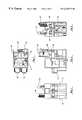
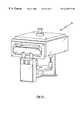
- FIG. 1is a left front perspective view of a complete assembly of a dual chamber version of the preferred embodiment of the present invention.
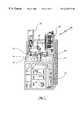
- FIG. 2is a rear perspective view of FIG. 1 .
- FIG. 3is a front elevation view of FIG. 1 .
- FIG. 4is a right side elevation view of FIG. 1 .
- FIG. 5is a rear elevation view of FIG. 1 .
- FIG. 6is a top plan view of FIG. 1 .
- FIG. 7is an enlarged view of FIG. 2 .
- FIG. 8is an enlarged view of the process gas distribution box of the present invention.
- FIG. 9is an enlarged view of the microwave generator of the present invention.
- FIG. 10is an enlarged view of the microwave switch of the present invention.
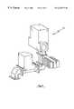
- FIG. 11is an enlarged view of one of the plasma sources of the present invention.
- FIG. 12is an enlarged view of one of the wafer process chambers of the present invention.
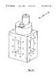
- FIGS. 13A-13Eare, respectively top plan, bottom plan, rear elevation, right side elevation and left side elevation views of one of the vacuum pumps of the present invention.
- FIG. 14is a general schematic flow diagram of a dual downstream reactor version of the present invention using a single vacuum pump.
- FIG. 15is a more detailed schematic flow diagram of a dual downstream reactor version of the present invention using a single vacuum pump and dual throttle valves.
- FIG. 16is a detailed schematic diagram of the pump/vent system of a dual downstream reactor version of the present invention using dual vacuum pumps and a single throttle valve.
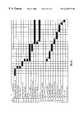
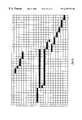
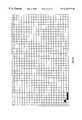
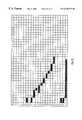
- FIG. 17is a line graph of a detailed task function timing diagram of a first working example of a dual, same single process, downstream reactors version of the present invention using two exterior (relative to the vacuum) 25-wafer cassettes and a single exterior robot with one front arm and one rear arm. The same sequence would be followed using a single 25-wafer cassette.
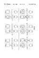
- FIG. 18is a schematic representation tracing the robot movements and processing of the working example of FIG. 17 using two cassettes.
- FIGS. 19-20are schematic representations showing the robot movements of a modified form of the present invention in a second working example in FIG. 17 in which the robot may be viewed as always standing with one arm on one side adjacent the chamber and the other arm on the other side adjacent the cassette and shuttling the wafers from one arm to the other to accomplish the specified function.
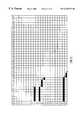
- FIG. 21is a schematic representation of how the individual enlarged line graphs of FIGS. 22-29, each of which shows a portion of a third working example of the present invention which is shown completely in FIG. 30, fit together to produce the single large line graph which is shown greatly reduced in FIG. 30 .
- FIG. 22is a line graph of a detailed task function timing diagram of a first portion of a second working example of a dual, same single process, downstream reactors version of the present invention using a single exterior (relative to the vacuum) 25-wafer cassette and a single exterior robot with two front (left and right) arms which is completely shown in FIG. 30 .
- FIG. 23is a line graph of a detailed task function timing diagram of a second portion of the working example of FIG. 30 .
- FIG. 24is a line graph of a detailed task function timing diagram of a third portion of the working example of FIG. 30 .
- FIG. 25is a line graph of a detailed task function timing diagram of a fourth portion of the working example of FIG. 30 .
- FIG. 26is a line graph of a detailed task function timing diagram of a fifth portion of the working example of FIG. 30 .
- FIG. 27is a line graph of a detailed task function timing diagram of a sixth portion of the working example of FIG. 30 .
- FIG. 28is a line graph of a detailed task function timing diagram of a seventh portion of the working example of FIG. 30 .
- FIG. 29is a line graph of a detailed task function timing diagram of a eighth portion of the working example of FIG. 30 .
- FIG. 30is a line graph of the complete detailed task function timing diagram of a second working example of a dual, same single process, downstream reactors version of the present invention using a single exterior (relative to the vacuum) 25-wafer cassette and a single exterior robot with two front (left and right) arms, eight separate portions of which are shown enlarged in FIGS. 22-29.
- FIG. 31is an enlarged perspective view of the dual armed robot used in the working example 3 of FIGS. 21-30 of the present invention.
- FIG. 32is a schematic plan view of a single plasma applicator alternately servicing dual processing chambers using a common diverter plate.
- the synchronous multiplexed near zero overhead system architecture 10 of the present inventionhas the typical set of one group of mass flow controllers controlling process gases 20 , microwave and RF power sources 22 , and optionally a single source of vacuum 34 .
- the key differenceis the addition of the second of two process reactor chamber 30 , 32 . Wafer processing alternates between the two process chambers 30 , 32 . While one reactor chamber 30 is processing a wafer, the other chamber 32 is being vented 43 (FIG. 15) back to atmosphere, the completed wafer is exchanged with a new unprocessed wafer, and the other chamber 32 is pumped back to the desired vacuum level. Optional wafer temperature conditioning 31 , 33 is performed just prior to pump down or during vacuum pump down. Process gases and vacuum sources are alternated 20 to the appropriate process chamber 30 , 32 along with the associated microwave or RF power sources 22 via a relay and/or microwave switch 24 .
- the robotic transfer overhead plus pump and vent overhead timeshould be less than the total active wafer processing time. (FIG. 17 ).
- a near 100% equipment utilization condition for active processis achieved versus the typical situation of 30% utilization, or even less for short process times.
- the additional process chamber 30 , 32adds to system cost, even so, the added amount represents only 10 to 20% of the total system cost.
- the present inventionincreases overall throughput substantially by roughly double the normal throughput of the prior art.
- the overall assembly 10 of the computer controlled, synchronous, multiplexed, near zero overhead, architecture for vacuum processes of the present inventionis shown in a preferred embodiment that includes in its most general form a computer shown in FIG. 7, a front panel 12 (FIGS. 1 , 3 ), at least one cassette 14 , 16 (FIGS. 1 , 3 , 6 ), a robot 15 (FIGS. 4 , 6 ), a back panel 18 (FIGS. 2 , 7 ), a process gas distribution box 20 (FIGS. 2 , 7 , 8 ), a microwave generator 22 (FIGS. 1 , 2 , 7 , 9 ), a microwave switch 24 ((FIGS.
- FIGS. 2 , 5 , 7 , 10at least one plasma source 26 , 28 (FIGS. 2 , 5 , 7 , 11 ) and at least two processing chambers 30 , 32 (FIGS. 1 , 7 , 12 ), and at least one vacuum pump 34 (FIGS. 7 , 13 ).
- the process chambers 30 , 32are identical single process chambers set up to run the same or similar process in a vacuum.
- the process cyclecan be best explained by examining the movements of the robot 15 . We can start by looking at the robot 15 in mid-cycle removing a previously processed wafer from one previously vented 20 chamber 30 with one gripper and replacing it with an unprocessed wafer previously removed from a cassette 14 , 16 (one or more cassettes may be used) with its other gripper.
- a vacuum 34is drawn in that chamber 30 and the active wafer processing begins there by igniting the plasma 26 for that chamber by switching 24 on the common microwave energy generator source 22 to it While the first wafer is being processed in the one chamber 30 , the robot 15 moves to the cassette 14 , 16 while the still hot processed wafer (in the case of photoresist ashing) it is carrying is cooled and loads that wafer into the cassette 14 , 16 while removing a second unprocessed wafer and turns to the now vented 20 other chamber 32 which has just finished processing a wafer also previously deposited in it. The robot 15 removes the processed wafer from the other chamber 32 replacing it with the second unprocessed wafer in its other gripper.
- the robotWhile the second wafer is being processed in the other chamber 32 , the robot again moves to the cassette 14 , 16 while the still hot processed wafer it is carrying is cooled and loads that wafer into the cassette 14 , 16 while removing a third unprocessed wafer and again turns back to the now vented 20 one chamber 30 which has just finished processing the first wafer, and the cycle repeats.
- the overheadis near zero if all chamber 30 , 32 overhead processes and robot 15 overhead processes (that is, all pre- and post-active processing preparatory steps) are begun and completed during the time that each chamber 30 , 32 alternately and synchronously begins and completes active processing of its wafer (between the time the power supply is switched on and the time the power supply is switched off).
- the power supply, vacuum pump and throttle valvecan all be shared by the dual chambers and used in alternation synchronously with the chambers 30 , 32 operations. Additionally, however, just as the aforesaid components may be shared, so too, can the other components of the system be shared, including , but not limited to, the end-point detector, the pressure transducers (manometers measuring pressures in the chambers), the gas box, the backfill pressure tank and lines, the reservoir and pressure equipment and lines and the like. Additionally, other configurations and sharing than those shown herein are possible.
- Plasma power sourcescome in many forms.
- microwave energyis used to excite the process gases at rarified pressures.
- additional power suppliesmay be used in the present invention to produce a plasma condition.
- the FCConly allows certain frequencies to be used for high power non-communications commercial applications while the vast majority of the radio frequency spectrum is reserved for communications.
- the RF frequencies used in commercial semiconductor applicationsare 100 KHz, 400 KHz, 13.56 MHZ, 915 MHZ, and 2.45 GHZ.
- the bands above 900 MHZare generally called microwave frequencies because of their very short wavelengths. But, in fact, they are all radio frequencies and it is the intent of the present invention to cover all applicable radio frequencies.
- the robotic interface to the process reactorscan also take on many forms.
- a single arm, dual gripperis used (one arm linkage, but ability to hold two wafers at a time).
- the preferred robotic formis a dual arm robot, such as is described below in working examples 3 (FIGS. 21 - 31 ), each with a single gripper to hold one wafer on each arm for an overall total of two wafers.
- a single arm linkage with one gripper to hold only one waferordinarily would be too slow for many applications, but may be acceptable for long processes.
- the particular configuration used in this applicationhas the cassettes and chambers on 90 degree X-Y coordinates which means that the robot moves in a straight line path perpendicular to a line joining a cassette on one side and a processing chamber on the other side, that is, in an aisle between the two cassettes on one gripper and the two chambers on the other gripper.
- the traverseris not needed.
- the robotis at the center and the cassettes and process reactors are on a fixed radius around it.
- Newer robotshave additional degrees of movement freedom to operate with cassettes and process reactors on 90 degree X-Y configurations, yet are located at a central fixed position. It is the intent of this application to cover all robot types.
- the process gases of the present inventionare selected and then flow through a plurality of lines according to the position of a plurality of valves mounted on the process gas distribution box 20 and which are under the control of a computer program (not shown). While the gases and the distribution hardware 20 used in the present invention are all conventional, the system architecture and the software processes which control the flow of gases therethrough are proprietary.
- Process gasesoriginate from a common source for both processing chambers 30 , 32 .
- the gas flowis alternately enabled through separate lines to each plasma applicator 26 , 28 and chamber 30 , 32 combination in synchronism with the loading of an unprocessed wafer therein by the robot 15 , the application of a vacuum by the common pump 34 in the chamber 30 , 32 , the heating of the wafer on the chuck 31 , 33 , the switching on by the common microwave switch 24 of the common microwave power supply 22 , the stabilization of the pressure in the chambers 30 , 32 by the throttle valves 36 , 37 , the venting 41 , 43 of the chambers 30 , 32 and the removal of the processed wafers from the chambers 30 , 32 by the robot 15 .
- the pumping system subsystem of the pump/vent system 40includes two pumps 96 , 98 and one throttle valve 94 for the two process chambers 70 , 72 .
- This architectureis based on the condition that only one of chambers 70 , 72 is running process at any one time.
- the appropriate one of stop valves 86 , 92is opened and wet pump 98 is operated.
- Manometer 64indicates the pressure in the chamber 70 , 72 which is processing by opening the appropriate one of stop valves 66 , 68 .
- the throttle valvewill close correspondingly if the chamber pressure is too low, and, will open appropriately if the chamber pressure is too high.
- the pump subsystem 96 , 98provides the following additional significant operating features and advantages when compared to one vacuum pump for one processing chamber setup:
- one of the two pumps 96 , 98is used solely for chamber pump-down while the other pump is used only during the processing of the wafer.
- wet pump 98For pumping down a chamber 70 , 72 , wet pump 98 is operated and the appropriate one of the stop valves 86 , 92 is opened while its associated stop valve 88 , 90 is closed.
- Wet pump 98requires oil for lubricating the pumping mechanism, and, therefore, it is highly possible that the chamber 70 , 72 may be contaminated by the lubrication oil due to back-streaming.
- oil back-streamingoccurs in higher vacuum conditions where fewer gas molecules exist in the pump line, and the oil molecules require some time to travel back-stream to the chamber 70 , 72 .
- the chamber pressureis reduced from 760 Torr to 1 Torr and a pump-down cycle is completed in 3 to 5 seconds. The higher pressure translates into a lot of gas molecules and creates a sweeping effect in a short period of time, virtually eliminating the back-streaming effect.
- the dry pump 96is operated with throttle valve 94 and the appropriate one of the stop valves 88 , 90 open and its associated pump down stop valve 86 , 92 closed.
- a dry pump 96is preferable for the processing pump because it does not require lubrication oil for the pumping mechanism, and, therefore, eliminates the possibility of process contamination by oil back-streaming to the processing chamber 70 , 72 through the pump line.
- the dry pump 96costs about twice as much as the wet pump 98 .
- the dry/wet pumping system setupreduces the overall cost of the system and efficiently utilizes the function of the pumps 96 , 98 .
- the throttle valve 94has to be wide open for a faster pump-down.
- the throttle valve 94starts to move to the throttling position while process gas starts to flow. It usually takes the throttle valve 94 about 5 seconds to control the chamber to reach the desired process pressure. Nearly this entire 5 seconds can be saved by bypassing the throttle valve 94 for pump-down, since the throttle valve can be preset at the desired position for a faster process pressure stabilization.
- the venting subsystem of the pump/vent system 40includes a source of N 2 gas which enters the system through a conventional gas box 42 having a pressure gauge 44 , a stop valve 46 , a pressure regulator 48 which is adjustable in a range, for example between 0-100 psig, a filter 50 , and a stop valve 52 .
- the gas box 42distributes the N2 gas to a pressurized back-fill tank 53 and then to chamber 70 through a pair of parallel valves 56 , 60 and to chamber 72 through a pair of parallel valves 58 , 62 .
- the miniconvectorns 78 , 80measure the pressure in the chambers 70 , 72 through valves 82 , 84 in a broad range from the base vacuum of a few mTorr to atmospheric level of 760 Torr.
- the vent subsystemprovides the following additional operating features and advantages:
- initial slow ventingis achieved by opening the appropriate one of the small orifice (.25 inches) valves 60 , 62 .
- the short initial slow venting step described in the preceding sectionis immediately followed by a fast venting which is achieved by shutting the small orifice valves 60 , 62 and opening the appropriate one of the large orifice valves 56 , 58 backfilling the chamber with N2 from the pressurized back-fill tank 53 which is kept at a preferred pressure of 30 psig on pressure gauge 54 .
- Ventingrequires a lot of N2. Without a pressurized tank 53 , if chamber 1 were venting while chamber 2 was running a process, the N2 pressure in the gas line to chamber 2 might drop, and, if it did, the process gas flow of chamber 2 might be disrupted. Pressurized back-fill tank 53 is equivalent to the capacitor of an electrical circuit where energy can be stored and released in a short period of time thereby minimizing process disruption.
- the venting subsystem of the pump/vent system 40can provide a gentle trickle purge of N2 gas through the bleed valve 60 , 62 (FIG. 16) to keep air and moisture from entering the chamber 70 , 72 .
- the gas going through the chamber being processedshould be at a higher pressure than what is in the line.
- the key to this workingis sufficiently long vacuum lines to provide isolation between the two process chambers.
- the vacuum linesshould be fairly large in diameter to provide more volume for the air to expand from the chamber being pumped down.
- a bypass valveis provided with a 1 ⁇ 4 inch line to slow the initial burst of air from the chamber being pumped down.
- the main ISO 80 valveis opened providing a higher conductance to rapidly pump the remaining air from the chamber.
- the fiber optic cabletransmits UV light from the chamber being processed. Again, since only one chamber at a time is processing a wafer, the two fiber optic cables go into an optical summing junction where the signals from the two chambers are added together. Obviously, only one produces UV light at a time, so an optical switch is unnecessary.
- the end point detectoris a monochromator which selects only one spectrum emission line, typically an OH line. End-point detectors are relatively expensive. Normally, one end-point detector is required per chamber.
- the line graphdisplays a task function along the Y coordinate and time along the X coordinate of a complete cycle of a first working example of one embodiment of the present invention in which two conventional downstream reactors each running the same or similar process are serviced by two exterior (relative to the vacuum) 25-wafer cassettes and a single exterior robot with one front arm and one rear arm. The same sequence would be followed using a single 25-wafer cassette.
- process reactorscan be different and still alternate overhead /process tasks. Wafers would be mapped cassette #1 to process chamber #1 and cassette #2 to process chamber #2.
- the process cyclecan be best explained by examining the movements of the robot 15 which are traced out schematically in FIG. 18 .
- the robot 15removes a previously processed wafer 1 from chamber 1 with his back gripper and rotates 180 degrees placing an unprocessed wafer 3 previously removed from cassette 1 (one or two cassettes may be used) with its front gripper.
- the chamber 1 dooris then closed its pins are lowered, a vacuum 34 is applied to the chuck 31 , the chamber 1 is pumped down, the process gas is turned on, the process gas is stabilized by adjusting the throttle valve 36 (or 94 in a single pump process (FIG. 16 )), and the active wafer 3 processing begins by igniting the plasma 26 for chamber 1 by switching 24 on the common microwave energy generator source 22 to it. Meanwhile from the point that the robot places the new wafer 3 into the chamber 1 for processing and thereafter while wafer 3 is being processed in chamber 1 , the robot traverses to cassette 2 and holds the still hot processed wafer 1 at the cooling station which is actually a heatsink area on the robot's body combined with cool air from blower 35 (FIG.
- the robotthen loads wafer 1 into the cassette 2 with its rear gripper, retracts and indexes to a new slot and removes unprocessed wafer 4 with the rear arm, and waits for the door to open of the now vented chamber 2 which has just finished processing a wafer 2 also previously deposited in it.
- the robot 15removes the processed wafer 2 from chamber 2 with its front gripper, rotates 180 degrees, places the unprocessed wafer 4 into chamber 2 with its rear gripper, traverses to cassette 1 while the still hot processed wafer 2 is cooled and loads wafer 2 into the cassette 1 , retracts and indexes and removes unprocessed wafer 5 and waits for the door to open to the now vented chamber 1 which has just finished processing the first wafer 3 .
- the cyclerepeats.
- the overheadis near zero if each chamber 1 , 2 alternately and synchronously finishes processing its wafer just as the robot 15 , finishes removing a fresh wafer from the cassette adjacent that chamber 1 , 2 with its one gripper ready for an exchange with its other gripper and the chamber overhead is shorter than the process time.
- the wait timeis zero, then the overhead is near zero and 100% utilization of the processing capacity of the machine is being realized. Achieving near zero wait time is simply a function of doing what is necessary to shorten and equalize the processing times in the adjacent chambers while speeding up the robot to finish his tasks in the same or similar amount of time.
- both cassettesare processing simultaneously, and all of the wafers are removed from one cassette before processing, but, are returned to the other cassette after processing.
- the robot movementsare those of a modified form of the working example of FIG. 17 but still similar in many respects.
- the robotmay be viewed as always standing facing toward chamber 2 and cassette 2 as seen in FIG. 19 step #1 with his left arm adjacent chamber 1 and the right arm adjacent cassette 1 and not turning 180 degrees to move a wafer from a cassette to a chamber, and, vice versa.
- working examples 1 and 2are identical.
- wafer 1is removed from cassette 1 (#1) and placed in chamber 1 for processing (#2); wafer 2 is removed from cassette 1 (#3) and placed in chamber 2 for processing (#4); wafer 3 is removed from cassette 1 (#5) and, as chamber 1 finishes processing, wafer 1 is removed from chamber 1 (#6) and replaced by wafer 3 (#7), and wafer 1 is stored in its original slot in cassette 1 (#8); wafer 4 is removed from cassette 1 (#9) and, as chamber 2 finishes processing, wafer 2 is removed from chamber 2 (#10) and replaced by wafer 4 (#11), and wafer 2 is stored in its original slot in cassette 1 (#12).
- the cyclerepeats.
- the movementsare those of a robot of a third working example of an embodiment of the present invention in which dual downstream or in-chamber reactors are each running the same single process using a single exterior (relative to the vacuum) 25-wafer cassette and a single exterior robot with two front arms (as was the robot of working example 2 in FIGS. 19 - 20 ), eight separate portions of which are shown enlarged in FIGS. 22-29 for ease in reading the function steps.
- all of the odd numbered wafersare processed in chamber 1 and all of the even numbered wafers are processed in chamber 2 , but all wafers are returned to their original slots in the single cassette. Otherwise, the process steps are the same as in the prior working examples. Microwave energy is used in this example.
- the sequenceis shown for a single cassette, actually the sequence can repeat relative to a cassette #2, #3, and #4, or even for 6 or more cassettes if desired.
- a set of specifications of the typical process results and typical operating parameters of the present inventionare as follows:
- Microwave power1,000 watts
- the present inventionmay still take further forms. For example, as seen in FIG. 32 further economies and reductions in overall cost may be achieved by using a single common plasma applicator 26 the output flow of plasma excited process gases from which are selectively directed alternately 100 to one of a pair of separate processing chambers 14 , 16 .
- the plasma exhaustwill be extremely hot, nonetheless, materials exist which could withstand this intense heat blast and not contaminate the downstream plasma excited process gases flow.
- a common diverter plateis constructed and is mounted adjacent the plasma exhaust and is mechanically electromechanically operated to alternately deflect the plasma exhaust in one path through an open very large orifice stop valve 104 to and in synchronism with the processing one of the two processing chambers while a very large orifice stop valve 102 is synchronously closed in the other path to the non-processing chamber, and vice versa.
- the complete elimination of one entire plasma applicatorfurther eliminates a costly redundancy and is in keeping with the objects of the present invention.
Landscapes
- Engineering & Computer Science (AREA)
- Physics & Mathematics (AREA)
- Condensed Matter Physics & Semiconductors (AREA)
- General Physics & Mathematics (AREA)
- Manufacturing & Machinery (AREA)
- Computer Hardware Design (AREA)
- Microelectronics & Electronic Packaging (AREA)
- Power Engineering (AREA)
- Drying Of Semiconductors (AREA)
- Container, Conveyance, Adherence, Positioning, Of Wafer (AREA)
Abstract
Description
Claims (45)
Priority Applications (8)
| Application Number | Priority Date | Filing Date | Title |
|---|---|---|---|
| US09/060,095US6228773B1 (en) | 1998-04-14 | 1998-04-14 | Synchronous multiplexed near zero overhead architecture for vacuum processes |
| KR10-2000-7011444AKR100477403B1 (en) | 1998-04-14 | 1999-04-13 | Synchronous multiplexed near zero overhead architecture for vacuum processes |
| JP2000544003AJP3874610B2 (en) | 1998-04-14 | 1999-04-13 | Synchronously multiplexed near-zero overhead architecture for vacuum processing |
| DE69937554TDE69937554T2 (en) | 1998-04-14 | 1999-04-13 | SYNCHRONOUS MULTIPLEXED ARCHITECTURE FOR VACUUM PROCESSING WITH A SURPLUS NEAR SULL |
| EP99917461AEP1074042B1 (en) | 1998-04-14 | 1999-04-13 | Synchronous multiplexed near zero overhead architecture for vacuum processes |
| PCT/US1999/008066WO1999053538A1 (en) | 1998-04-14 | 1999-04-13 | Synchronous multiplexed near zero overhead architecture for vacuum processes |
| AU35578/99AAU3557899A (en) | 1998-04-14 | 1999-04-13 | Synchronous multiplexed near zero overhead architecture for vacuum processes |
| US09/314,193US6273956B1 (en) | 1998-04-14 | 1999-05-19 | Synchronous multiplexed near zero overhead architecture for vacuum processes |
Applications Claiming Priority (1)
| Application Number | Priority Date | Filing Date | Title |
|---|---|---|---|
| US09/060,095US6228773B1 (en) | 1998-04-14 | 1998-04-14 | Synchronous multiplexed near zero overhead architecture for vacuum processes |
Publications (1)
| Publication Number | Publication Date |
|---|---|
| US6228773B1true US6228773B1 (en) | 2001-05-08 |
Family
ID=22027326
Family Applications (2)
| Application Number | Title | Priority Date | Filing Date |
|---|---|---|---|
| US09/060,095Expired - LifetimeUS6228773B1 (en) | 1998-04-14 | 1998-04-14 | Synchronous multiplexed near zero overhead architecture for vacuum processes |
| US09/314,193Expired - LifetimeUS6273956B1 (en) | 1998-04-14 | 1999-05-19 | Synchronous multiplexed near zero overhead architecture for vacuum processes |
Family Applications After (1)
| Application Number | Title | Priority Date | Filing Date |
|---|---|---|---|
| US09/314,193Expired - LifetimeUS6273956B1 (en) | 1998-04-14 | 1999-05-19 | Synchronous multiplexed near zero overhead architecture for vacuum processes |
Country Status (7)
| Country | Link |
|---|---|
| US (2) | US6228773B1 (en) |
| EP (1) | EP1074042B1 (en) |
| JP (1) | JP3874610B2 (en) |
| KR (1) | KR100477403B1 (en) |
| AU (1) | AU3557899A (en) |
| DE (1) | DE69937554T2 (en) |
| WO (1) | WO1999053538A1 (en) |
Cited By (35)
| Publication number | Priority date | Publication date | Assignee | Title |
|---|---|---|---|---|
| US20030127107A1 (en)* | 2002-01-07 | 2003-07-10 | Taiwan Semiconductor Manufacturing Co., Ltd. | Apparatus and method for removing coating layers from alignment marks |
| US6660094B2 (en)* | 2001-05-30 | 2003-12-09 | Canon Kabushiki Kaisha | Apparatus and method for forming deposited film |
| US20040001295A1 (en)* | 2002-05-08 | 2004-01-01 | Satyendra Kumar | Plasma generation and processing with multiple radiation sources |
| WO2004010482A1 (en)* | 2002-07-19 | 2004-01-29 | Axcelis Technologies, Inc. | Dual chamber vacuum processing system |
| US20040086641A1 (en)* | 2000-05-31 | 2004-05-06 | Hirokazu Otoshi | Apparatus and method for forming deposited film |
| US20040107796A1 (en)* | 2002-12-04 | 2004-06-10 | Satyendra Kumar | Plasma-assisted melting |
| US20050000434A1 (en)* | 2001-02-26 | 2005-01-06 | Lee Chung J. | Reactor for producing reactive intermediates for low dielectric constant polymer thin films |
| US20050016956A1 (en)* | 2003-03-14 | 2005-01-27 | Xinye Liu | Methods and apparatus for cycle time improvements for atomic layer deposition |
| US20050205210A1 (en)* | 2004-01-06 | 2005-09-22 | Devine Daniel J | Advanced multi-pressure workpiece processing |
| US20050233091A1 (en)* | 2002-05-08 | 2005-10-20 | Devendra Kumar | Plasma-assisted coating |
| US20050253529A1 (en)* | 2002-05-08 | 2005-11-17 | Satyendra Kumar | Plasma-assisted gas production |
| US20050271829A1 (en)* | 2002-05-08 | 2005-12-08 | Satyendra Kumar | Plasma-assisted formation of carbon structures |
| US20060057016A1 (en)* | 2002-05-08 | 2006-03-16 | Devendra Kumar | Plasma-assisted sintering |
| US20060124613A1 (en)* | 2002-05-08 | 2006-06-15 | Satyendra Kumar | Plasma-assisted heat treatment |
| US20060228497A1 (en)* | 2002-05-08 | 2006-10-12 | Satyendra Kumar | Plasma-assisted coating |
| US20060231983A1 (en)* | 2002-05-08 | 2006-10-19 | Hiroko Kondo | Method of decorating large plastic 3d objects |
| US20060233682A1 (en)* | 2002-05-08 | 2006-10-19 | Cherian Kuruvilla A | Plasma-assisted engine exhaust treatment |
| US20060237398A1 (en)* | 2002-05-08 | 2006-10-26 | Dougherty Mike L Sr | Plasma-assisted processing in a manufacturing line |
| US20080129208A1 (en)* | 2004-11-05 | 2008-06-05 | Satyendra Kumar | Atmospheric Processing Using Microwave-Generated Plasmas |
| US7432470B2 (en) | 2002-05-08 | 2008-10-07 | Btu International, Inc. | Surface cleaning and sterilization |
| US7465362B2 (en) | 2002-05-08 | 2008-12-16 | Btu International, Inc. | Plasma-assisted nitrogen surface-treatment |
| US7494904B2 (en) | 2002-05-08 | 2009-02-24 | Btu International, Inc. | Plasma-assisted doping |
| US7498066B2 (en) | 2002-05-08 | 2009-03-03 | Btu International Inc. | Plasma-assisted enhanced coating |
| US20090102292A1 (en)* | 2007-09-19 | 2009-04-23 | Nigel Power, Llc | Biological Effects of Magnetic Power Transfer |
| US7560657B2 (en) | 2002-05-08 | 2009-07-14 | Btu International Inc. | Plasma-assisted processing in a manufacturing line |
| US20110100554A1 (en)* | 2009-09-09 | 2011-05-05 | Applied Materials, Inc. | Parallel system for epitaxial chemical vapor deposition |
| US20110266256A1 (en)* | 2010-04-30 | 2011-11-03 | Applied Materials, Inc. | Methods for processing substrates in process systems having shared resources |
| US20120031330A1 (en)* | 2010-08-04 | 2012-02-09 | Toshiro Tsumori | Semiconductor substrate manufacturing apparatus |
| US20120192793A1 (en)* | 2011-02-01 | 2012-08-02 | Tokyo Electron Limited | Film forming apparatus |
| US20140295083A1 (en)* | 2013-03-29 | 2014-10-02 | Tokyo Electron Limited | Film forming apparatus, gas supply device and film forming method |
| US20160281236A1 (en)* | 2015-03-26 | 2016-09-29 | Alta Devices, Inc. | Substrate processing using interleaved load lock transfers |
| US20200256228A1 (en)* | 2019-02-13 | 2020-08-13 | Applied Materials, Inc. | Vacuum Pumps For Single And Multi-Process Chamber Flow Stream Sharing |
| WO2020214618A1 (en)* | 2019-04-19 | 2020-10-22 | Lam Research Corporation | Foreline assembly for quad station process module |
| US20220336260A1 (en)* | 2021-04-19 | 2022-10-20 | Tokyo Electron Limited | Substrate transfer device and substrate transfer method |
| US20230402983A1 (en)* | 2022-06-14 | 2023-12-14 | Semes Co., Ltd. | Microwave providing apparatus, system including the same, and method of manufacturing semiconductor device |
Families Citing this family (11)
| Publication number | Priority date | Publication date | Assignee | Title |
|---|---|---|---|---|
| US6630053B2 (en)* | 2000-08-22 | 2003-10-07 | Asm Japan K.K. | Semiconductor processing module and apparatus |
| US20090001524A1 (en)* | 2001-11-26 | 2009-01-01 | Siegele Stephen H | Generation and distribution of a fluorine gas |
| JP2005286102A (en)* | 2004-03-30 | 2005-10-13 | Hitachi High-Technologies Corp | Vacuum processing apparatus and vacuum processing method |
| US7467916B2 (en)* | 2005-03-08 | 2008-12-23 | Asm Japan K.K. | Semiconductor-manufacturing apparatus equipped with cooling stage and semiconductor-manufacturing method using same |
| KR101412063B1 (en)* | 2007-09-02 | 2014-07-18 | 주식회사 뉴파워 프라즈마 | Improved high speed substrate processing system with low cost and high productivity |
| US20090206056A1 (en)* | 2008-02-14 | 2009-08-20 | Songlin Xu | Method and Apparatus for Plasma Process Performance Matching in Multiple Wafer Chambers |
| DE102017214687A1 (en)* | 2017-08-22 | 2019-02-28 | centrotherm international AG | Processing apparatus for substrates and method for operating such a treatment apparatus |
| JP7033950B2 (en)* | 2018-02-19 | 2022-03-11 | 東京エレクトロン株式会社 | Gas distributor and processing equipment |
| DE102018112853A1 (en)* | 2018-05-29 | 2019-12-05 | Meyer Burger (Germany) Gmbh | Ventilation device and vacuum production plant |
| US11631583B2 (en)* | 2019-10-25 | 2023-04-18 | Applied Materials, Inc. | RF power source operation in plasma enhanced processes |
| JP6815542B2 (en)* | 2020-02-04 | 2021-01-20 | 東京エレクトロン株式会社 | Board processing equipment |
Citations (24)
| Publication number | Priority date | Publication date | Assignee | Title |
|---|---|---|---|---|
| US4105916A (en) | 1977-02-28 | 1978-08-08 | Extranuclear Laboratories, Inc. | Methods and apparatus for simultaneously producing and electronically separating the chemical ionization mass spectrum and the electron impact ionization mass spectrum of the same sample material |
| US4149923A (en) | 1977-07-18 | 1979-04-17 | Tokyo Ohka Kogyo Kabushiki Kaisha | Apparatus for the treatment of wafer materials by plasma reaction |
| US4483651A (en) | 1980-08-14 | 1984-11-20 | Tokyo Ohka Kogyo Kabushiki Kaisha | Automatic apparatus for continuous treatment of leaf materials with gas plasma |
| US4560417A (en) | 1981-12-30 | 1985-12-24 | Technomex Development, Ltd. | Decontamination method for semiconductor wafer handling equipment |
| US4638176A (en) | 1985-08-01 | 1987-01-20 | Mullett Associates, Inc. | Uninterruptible power supply |
| US4640224A (en) | 1985-08-05 | 1987-02-03 | Spectrum Cvd, Inc. | CVD heat source |
| US4692343A (en) | 1985-08-05 | 1987-09-08 | Spectrum Cvd, Inc. | Plasma enhanced CVD |
| US4702205A (en) | 1984-03-06 | 1987-10-27 | David Constant V | External combustion vane engine with conformable vanes |
| US5000682A (en) | 1990-01-22 | 1991-03-19 | Semitherm | Vertical thermal processor for semiconductor wafers |
| US5019233A (en) | 1988-10-31 | 1991-05-28 | Eaton Corporation | Sputtering system |
| US5138973A (en)* | 1987-07-16 | 1992-08-18 | Texas Instruments Incorporated | Wafer processing apparatus having independently controllable energy sources |
| US5225771A (en) | 1988-05-16 | 1993-07-06 | Dri Technology Corp. | Making and testing an integrated circuit using high density probe points |
| US5292393A (en)* | 1986-12-19 | 1994-03-08 | Applied Materials, Inc. | Multichamber integrated process system |
| US5310410A (en) | 1990-04-06 | 1994-05-10 | Sputtered Films, Inc. | Method for processing semi-conductor wafers in a multiple vacuum and non-vacuum chamber apparatus |
| US5338423A (en) | 1992-11-06 | 1994-08-16 | Zilog, Inc. | Method of eliminating metal voiding in a titanium nitride/aluminum processing |
| US5488967A (en) | 1993-10-27 | 1996-02-06 | Masako Kiyohara | Method and apparatus for feeding gas into a chamber |
| US5515986A (en)* | 1993-05-03 | 1996-05-14 | Balzers Aktiengesellschaft | Plasma treatment apparatus and method for operating same |
| US5567268A (en)* | 1994-01-31 | 1996-10-22 | Sony Corporation | Plasma processing apparatus and method for carrying out plasma processing by using such plasma processing apparatus |
| US5587182A (en) | 1994-02-21 | 1996-12-24 | Maschinenfabrik Hennecke Gmbh | Apparatus for the production of endless polyurethane moldings |
| US5595482A (en) | 1994-10-27 | 1997-01-21 | Parsons; Marshall F. | Airlocking system and method for feeding bulk granular material |
| US5611861A (en)* | 1995-05-31 | 1997-03-18 | Nec Corporation | Rotary type apparatus for processing semiconductor wafers and method of processing semiconductor wafers |
| US5755888A (en)* | 1994-09-01 | 1998-05-26 | Matsushita Electric Industrial Co., Ltd. | Method and apparatus of forming thin films |
| US5855681A (en)* | 1996-11-18 | 1999-01-05 | Applied Materials, Inc. | Ultra high throughput wafer vacuum processing system |
| US5900105A (en) | 1996-07-09 | 1999-05-04 | Gamma Precision Technology, Inc. | Wafer transfer system and method of using the same |
Family Cites Families (7)
| Publication number | Priority date | Publication date | Assignee | Title |
|---|---|---|---|---|
| JPS59112623A (en)* | 1982-12-17 | 1984-06-29 | Matsushita Electric Ind Co Ltd | Dry etching apparatus |
| JPS63115326A (en)* | 1986-10-31 | 1988-05-19 | Shimadzu Corp | Plasma cvd system |
| JP2787503B2 (en)* | 1990-02-26 | 1998-08-20 | 住友重機械工業株式会社 | Plasma processing equipment |
| KR100230697B1 (en)* | 1992-02-18 | 1999-11-15 | 이노우에 쥰이치 | Decompression unit |
| US5647945A (en)* | 1993-08-25 | 1997-07-15 | Tokyo Electron Limited | Vacuum processing apparatus |
| JPH08127861A (en)* | 1994-10-28 | 1996-05-21 | Tokyo Electron Ltd | Vacuum treating device |
| JP3947761B2 (en)* | 1996-09-26 | 2007-07-25 | 株式会社日立国際電気 | Substrate processing apparatus, substrate transfer machine, and substrate processing method |
- 1998
- 1998-04-14USUS09/060,095patent/US6228773B1/ennot_activeExpired - Lifetime
- 1999
- 1999-04-13AUAU35578/99Apatent/AU3557899A/ennot_activeAbandoned
- 1999-04-13JPJP2000544003Apatent/JP3874610B2/ennot_activeExpired - Fee Related
- 1999-04-13EPEP99917461Apatent/EP1074042B1/ennot_activeExpired - Lifetime
- 1999-04-13KRKR10-2000-7011444Apatent/KR100477403B1/ennot_activeExpired - Fee Related
- 1999-04-13DEDE69937554Tpatent/DE69937554T2/ennot_activeExpired - Fee Related
- 1999-04-13WOPCT/US1999/008066patent/WO1999053538A1/enactiveIP Right Grant
- 1999-05-19USUS09/314,193patent/US6273956B1/ennot_activeExpired - Lifetime
Patent Citations (24)
| Publication number | Priority date | Publication date | Assignee | Title |
|---|---|---|---|---|
| US4105916A (en) | 1977-02-28 | 1978-08-08 | Extranuclear Laboratories, Inc. | Methods and apparatus for simultaneously producing and electronically separating the chemical ionization mass spectrum and the electron impact ionization mass spectrum of the same sample material |
| US4149923A (en) | 1977-07-18 | 1979-04-17 | Tokyo Ohka Kogyo Kabushiki Kaisha | Apparatus for the treatment of wafer materials by plasma reaction |
| US4483651A (en) | 1980-08-14 | 1984-11-20 | Tokyo Ohka Kogyo Kabushiki Kaisha | Automatic apparatus for continuous treatment of leaf materials with gas plasma |
| US4560417A (en) | 1981-12-30 | 1985-12-24 | Technomex Development, Ltd. | Decontamination method for semiconductor wafer handling equipment |
| US4702205A (en) | 1984-03-06 | 1987-10-27 | David Constant V | External combustion vane engine with conformable vanes |
| US4638176A (en) | 1985-08-01 | 1987-01-20 | Mullett Associates, Inc. | Uninterruptible power supply |
| US4640224A (en) | 1985-08-05 | 1987-02-03 | Spectrum Cvd, Inc. | CVD heat source |
| US4692343A (en) | 1985-08-05 | 1987-09-08 | Spectrum Cvd, Inc. | Plasma enhanced CVD |
| US5292393A (en)* | 1986-12-19 | 1994-03-08 | Applied Materials, Inc. | Multichamber integrated process system |
| US5138973A (en)* | 1987-07-16 | 1992-08-18 | Texas Instruments Incorporated | Wafer processing apparatus having independently controllable energy sources |
| US5225771A (en) | 1988-05-16 | 1993-07-06 | Dri Technology Corp. | Making and testing an integrated circuit using high density probe points |
| US5019233A (en) | 1988-10-31 | 1991-05-28 | Eaton Corporation | Sputtering system |
| US5000682A (en) | 1990-01-22 | 1991-03-19 | Semitherm | Vertical thermal processor for semiconductor wafers |
| US5310410A (en) | 1990-04-06 | 1994-05-10 | Sputtered Films, Inc. | Method for processing semi-conductor wafers in a multiple vacuum and non-vacuum chamber apparatus |
| US5338423A (en) | 1992-11-06 | 1994-08-16 | Zilog, Inc. | Method of eliminating metal voiding in a titanium nitride/aluminum processing |
| US5515986A (en)* | 1993-05-03 | 1996-05-14 | Balzers Aktiengesellschaft | Plasma treatment apparatus and method for operating same |
| US5488967A (en) | 1993-10-27 | 1996-02-06 | Masako Kiyohara | Method and apparatus for feeding gas into a chamber |
| US5567268A (en)* | 1994-01-31 | 1996-10-22 | Sony Corporation | Plasma processing apparatus and method for carrying out plasma processing by using such plasma processing apparatus |
| US5587182A (en) | 1994-02-21 | 1996-12-24 | Maschinenfabrik Hennecke Gmbh | Apparatus for the production of endless polyurethane moldings |
| US5755888A (en)* | 1994-09-01 | 1998-05-26 | Matsushita Electric Industrial Co., Ltd. | Method and apparatus of forming thin films |
| US5595482A (en) | 1994-10-27 | 1997-01-21 | Parsons; Marshall F. | Airlocking system and method for feeding bulk granular material |
| US5611861A (en)* | 1995-05-31 | 1997-03-18 | Nec Corporation | Rotary type apparatus for processing semiconductor wafers and method of processing semiconductor wafers |
| US5900105A (en) | 1996-07-09 | 1999-05-04 | Gamma Precision Technology, Inc. | Wafer transfer system and method of using the same |
| US5855681A (en)* | 1996-11-18 | 1999-01-05 | Applied Materials, Inc. | Ultra high throughput wafer vacuum processing system |
Cited By (62)
| Publication number | Priority date | Publication date | Assignee | Title |
|---|---|---|---|---|
| US7001640B2 (en) | 2000-05-31 | 2006-02-21 | Canon Kabushiki Kaisha | Apparatus and method for forming deposited film |
| US20040086641A1 (en)* | 2000-05-31 | 2004-05-06 | Hirokazu Otoshi | Apparatus and method for forming deposited film |
| US20050000434A1 (en)* | 2001-02-26 | 2005-01-06 | Lee Chung J. | Reactor for producing reactive intermediates for low dielectric constant polymer thin films |
| US6660094B2 (en)* | 2001-05-30 | 2003-12-09 | Canon Kabushiki Kaisha | Apparatus and method for forming deposited film |
| US20030127107A1 (en)* | 2002-01-07 | 2003-07-10 | Taiwan Semiconductor Manufacturing Co., Ltd. | Apparatus and method for removing coating layers from alignment marks |
| US7445817B2 (en) | 2002-05-08 | 2008-11-04 | Btu International Inc. | Plasma-assisted formation of carbon structures |
| US20060233682A1 (en)* | 2002-05-08 | 2006-10-19 | Cherian Kuruvilla A | Plasma-assisted engine exhaust treatment |
| US20040118816A1 (en)* | 2002-05-08 | 2004-06-24 | Satyendra Kumar | Plasma catalyst |
| US7560657B2 (en) | 2002-05-08 | 2009-07-14 | Btu International Inc. | Plasma-assisted processing in a manufacturing line |
| US7498066B2 (en) | 2002-05-08 | 2009-03-03 | Btu International Inc. | Plasma-assisted enhanced coating |
| US20050061446A1 (en)* | 2002-05-08 | 2005-03-24 | Dana Corporation | Plasma-assisted joining |
| US7638727B2 (en) | 2002-05-08 | 2009-12-29 | Btu International Inc. | Plasma-assisted heat treatment |
| US20050233091A1 (en)* | 2002-05-08 | 2005-10-20 | Devendra Kumar | Plasma-assisted coating |
| US20050253529A1 (en)* | 2002-05-08 | 2005-11-17 | Satyendra Kumar | Plasma-assisted gas production |
| US20050271829A1 (en)* | 2002-05-08 | 2005-12-08 | Satyendra Kumar | Plasma-assisted formation of carbon structures |
| US7497922B2 (en) | 2002-05-08 | 2009-03-03 | Btu International, Inc. | Plasma-assisted gas production |
| US20060057016A1 (en)* | 2002-05-08 | 2006-03-16 | Devendra Kumar | Plasma-assisted sintering |
| US20060124613A1 (en)* | 2002-05-08 | 2006-06-15 | Satyendra Kumar | Plasma-assisted heat treatment |
| US20060228497A1 (en)* | 2002-05-08 | 2006-10-12 | Satyendra Kumar | Plasma-assisted coating |
| US20060231983A1 (en)* | 2002-05-08 | 2006-10-19 | Hiroko Kondo | Method of decorating large plastic 3d objects |
| US7494904B2 (en) | 2002-05-08 | 2009-02-24 | Btu International, Inc. | Plasma-assisted doping |
| US20060237398A1 (en)* | 2002-05-08 | 2006-10-26 | Dougherty Mike L Sr | Plasma-assisted processing in a manufacturing line |
| US7132621B2 (en) | 2002-05-08 | 2006-11-07 | Dana Corporation | Plasma catalyst |
| US20060249367A1 (en)* | 2002-05-08 | 2006-11-09 | Satyendra Kumar | Plasma catalyst |
| US7608798B2 (en) | 2002-05-08 | 2009-10-27 | Btu International Inc. | Plasma catalyst |
| US7214280B2 (en) | 2002-05-08 | 2007-05-08 | Btu International Inc. | Plasma-assisted decrystallization |
| US7227097B2 (en) | 2002-05-08 | 2007-06-05 | Btu International, Inc. | Plasma generation and processing with multiple radiation sources |
| US20070164680A1 (en)* | 2002-05-08 | 2007-07-19 | Satyendra Kumar | Plasma generation and processing with multiple radiation sources |
| US7309843B2 (en) | 2002-05-08 | 2007-12-18 | Btu International, Inc. | Plasma-assisted joining |
| US7592564B2 (en) | 2002-05-08 | 2009-09-22 | Btu International Inc. | Plasma generation and processing with multiple radiation sources |
| US7432470B2 (en) | 2002-05-08 | 2008-10-07 | Btu International, Inc. | Surface cleaning and sterilization |
| US20040001295A1 (en)* | 2002-05-08 | 2004-01-01 | Satyendra Kumar | Plasma generation and processing with multiple radiation sources |
| US7465362B2 (en) | 2002-05-08 | 2008-12-16 | Btu International, Inc. | Plasma-assisted nitrogen surface-treatment |
| WO2004010482A1 (en)* | 2002-07-19 | 2004-01-29 | Axcelis Technologies, Inc. | Dual chamber vacuum processing system |
| US20040089227A1 (en)* | 2002-07-19 | 2004-05-13 | Albert Wang | Dual chamber vacuum processing system |
| US20040107796A1 (en)* | 2002-12-04 | 2004-06-10 | Satyendra Kumar | Plasma-assisted melting |
| US7189940B2 (en) | 2002-12-04 | 2007-03-13 | Btu International Inc. | Plasma-assisted melting |
| US20050016956A1 (en)* | 2003-03-14 | 2005-01-27 | Xinye Liu | Methods and apparatus for cycle time improvements for atomic layer deposition |
| US20050205210A1 (en)* | 2004-01-06 | 2005-09-22 | Devine Daniel J | Advanced multi-pressure workpiece processing |
| US20080129208A1 (en)* | 2004-11-05 | 2008-06-05 | Satyendra Kumar | Atmospheric Processing Using Microwave-Generated Plasmas |
| US8614526B2 (en)* | 2007-09-19 | 2013-12-24 | Qualcomm Incorporated | System and method for magnetic power transfer |
| US20090102292A1 (en)* | 2007-09-19 | 2009-04-23 | Nigel Power, Llc | Biological Effects of Magnetic Power Transfer |
| US20110100554A1 (en)* | 2009-09-09 | 2011-05-05 | Applied Materials, Inc. | Parallel system for epitaxial chemical vapor deposition |
| US8721798B2 (en)* | 2010-04-30 | 2014-05-13 | Applied Materials, Inc. | Methods for processing substrates in process systems having shared resources |
| US8496756B2 (en)* | 2010-04-30 | 2013-07-30 | Applied Materials, Inc. | Methods for processing substrates in process systems having shared resources |
| US20110266256A1 (en)* | 2010-04-30 | 2011-11-03 | Applied Materials, Inc. | Methods for processing substrates in process systems having shared resources |
| TWI487053B (en)* | 2010-04-30 | 2015-06-01 | Applied Materials Inc | Methods for processing substrates in process systems having shared resources |
| WO2011136982A3 (en)* | 2010-04-30 | 2012-02-16 | Applied Materials, Inc. | Methods for processing substrates in process systems having shared resources |
| US20120031330A1 (en)* | 2010-08-04 | 2012-02-09 | Toshiro Tsumori | Semiconductor substrate manufacturing apparatus |
| US9139933B2 (en)* | 2010-08-04 | 2015-09-22 | Nuflare Technology, Inc. | Semiconductor substrate manufacturing apparatus |
| US20120192793A1 (en)* | 2011-02-01 | 2012-08-02 | Tokyo Electron Limited | Film forming apparatus |
| US9644266B2 (en)* | 2013-03-29 | 2017-05-09 | Tokyo Electron Limited | Film forming apparatus, gas supply device and film forming method |
| US20140295083A1 (en)* | 2013-03-29 | 2014-10-02 | Tokyo Electron Limited | Film forming apparatus, gas supply device and film forming method |
| US20160281236A1 (en)* | 2015-03-26 | 2016-09-29 | Alta Devices, Inc. | Substrate processing using interleaved load lock transfers |
| US20200256228A1 (en)* | 2019-02-13 | 2020-08-13 | Applied Materials, Inc. | Vacuum Pumps For Single And Multi-Process Chamber Flow Stream Sharing |
| WO2020168021A1 (en)* | 2019-02-13 | 2020-08-20 | Applied Materials, Inc. | Vacuum pumps for single and multi-process chamber flow stream sharing |
| TWI846819B (en)* | 2019-02-13 | 2024-07-01 | 美商應用材料股份有限公司 | Vacuum pumps for single and multi-process chamber flow stream sharing |
| WO2020214618A1 (en)* | 2019-04-19 | 2020-10-22 | Lam Research Corporation | Foreline assembly for quad station process module |
| US12362206B2 (en) | 2019-04-19 | 2025-07-15 | Lam Research Corporation | Foreline assembly for quad station process module |
| US20220336260A1 (en)* | 2021-04-19 | 2022-10-20 | Tokyo Electron Limited | Substrate transfer device and substrate transfer method |
| US12322642B2 (en)* | 2021-04-19 | 2025-06-03 | Tokyo Electron Limited | Substrate transfer device and substrate transfer method |
| US20230402983A1 (en)* | 2022-06-14 | 2023-12-14 | Semes Co., Ltd. | Microwave providing apparatus, system including the same, and method of manufacturing semiconductor device |
Also Published As
| Publication number | Publication date |
|---|---|
| JP3874610B2 (en) | 2007-01-31 |
| DE69937554T2 (en) | 2008-09-18 |
| EP1074042B1 (en) | 2007-11-14 |
| JP2002511651A (en) | 2002-04-16 |
| WO1999053538A1 (en) | 1999-10-21 |
| EP1074042A4 (en) | 2004-12-29 |
| DE69937554D1 (en) | 2007-12-27 |
| US6273956B1 (en) | 2001-08-14 |
| KR100477403B1 (en) | 2005-03-22 |
| EP1074042A1 (en) | 2001-02-07 |
| AU3557899A (en) | 1999-11-01 |
| KR20010042722A (en) | 2001-05-25 |
Similar Documents
| Publication | Publication Date | Title |
|---|---|---|
| US6228773B1 (en) | Synchronous multiplexed near zero overhead architecture for vacuum processes | |
| US5900105A (en) | Wafer transfer system and method of using the same | |
| US6007675A (en) | Wafer transfer system and method of using the same | |
| US11443952B2 (en) | Etching method and etching device | |
| US5709757A (en) | Film forming and dry cleaning apparatus and method | |
| WO1998001378A9 (en) | A wafer transfer system and method of using the same | |
| CN110112053A (en) | Combined treatment chamber and disposition chamber | |
| US6224680B1 (en) | Wafer transfer system | |
| KR20060081377A (en) | Substrate Processing System and Substrate Processing Program | |
| US10550469B2 (en) | Plasma excitation for spatial atomic layer deposition (ALD) reactors | |
| JP7671696B2 (en) | Multi-station semiconductor processing using independently adjustable pedestals - Patents.com | |
| JP7349861B2 (en) | Etching methods, damaged layer removal methods, and storage media | |
| KR20010062414A (en) | Serial wafer handling mechanism | |
| US12308219B2 (en) | Substrate treating method and substrate treating apparatus | |
| KR20210020808A (en) | Substrate processing method, pressure control apparatus and substrate processing system | |
| KR100722016B1 (en) | Substrate treating apparatus and method of substrate treatment | |
| US20180061616A1 (en) | Low pressure lift pin cavity hardware | |
| US20030029833A1 (en) | High speed photoresist stripping chamber | |
| KR20210015710A (en) | Substrate processing method, substrate processing apparatus and cleaning apparatus | |
| JP2006245312A (en) | Manufacturing method of semiconductor device | |
| JP4126229B2 (en) | Plasma generating apparatus and method | |
| KR102052337B1 (en) | Substrate treating apparatus and substrate treating method | |
| US20240337449A1 (en) | Regenerator for foreline heating | |
| US11302550B2 (en) | Transfer method | |
| KR20230101647A (en) | Apparatus for treating substrate and method for processing a substrate |
Legal Events
| Date | Code | Title | Description |
|---|---|---|---|
| AS | Assignment | Owner name:MATRIX INTEGRATED SYSTEMS, INC., CALIFORNIA Free format text:ASSIGNMENT OF ASSIGNORS INTEREST;ASSIGNOR:GERALD, M. COX;REEL/FRAME:009104/0537 Effective date:19980414 | |
| STCF | Information on status: patent grant | Free format text:PATENTED CASE | |
| FEPP | Fee payment procedure | Free format text:PAYOR NUMBER ASSIGNED (ORIGINAL EVENT CODE: ASPN); ENTITY STATUS OF PATENT OWNER: LARGE ENTITY | |
| AS | Assignment | Owner name:EXCELIS TECHNOLOGIES, INC., MASSACHUSETTS Free format text:ASSIGNMENT OF ASSIGNORS INTEREST;ASSIGNOR:MATRIX INTEGRATED SYSTEMS, INC.;REEL/FRAME:014885/0260 Effective date:20031130 | |
| FPAY | Fee payment | Year of fee payment:4 | |
| FEPP | Fee payment procedure | Free format text:PAT HOLDER NO LONGER CLAIMS SMALL ENTITY STATUS, ENTITY STATUS SET TO UNDISCOUNTED (ORIGINAL EVENT CODE: STOL); ENTITY STATUS OF PATENT OWNER: LARGE ENTITY | |
| REFU | Refund | Free format text:REFUND - SURCHARGE, PETITION TO ACCEPT PYMT AFTER EXP, UNINTENTIONAL (ORIGINAL EVENT CODE: R2551); ENTITY STATUS OF PATENT OWNER: LARGE ENTITY | |
| FEPP | Fee payment procedure | Free format text:PAYER NUMBER DE-ASSIGNED (ORIGINAL EVENT CODE: RMPN); ENTITY STATUS OF PATENT OWNER: LARGE ENTITY Free format text:PAYOR NUMBER ASSIGNED (ORIGINAL EVENT CODE: ASPN); ENTITY STATUS OF PATENT OWNER: LARGE ENTITY | |
| AS | Assignment | Owner name:SILICON VALLEY BANK, CALIFORNIA Free format text:SECURITY AGREEMENT;ASSIGNOR:AXCELIS TECHNOLOGIES, INC.;REEL/FRAME:020986/0143 Effective date:20080423 Owner name:SILICON VALLEY BANK,CALIFORNIA Free format text:SECURITY AGREEMENT;ASSIGNOR:AXCELIS TECHNOLOGIES, INC.;REEL/FRAME:020986/0143 Effective date:20080423 | |
| FPAY | Fee payment | Year of fee payment:8 | |
| FPAY | Fee payment | Year of fee payment:12 | |
| AS | Assignment | Owner name:LAM RESEARCH CORPORATION, CALIFORNIA Free format text:ASSIGNMENT OF ASSIGNORS INTEREST;ASSIGNOR:AXCELIS TECHNOLOGIES, INC.;REEL/FRAME:029529/0757 Effective date:20121203 | |
| AS | Assignment | Owner name:AXCELIS TECHNOLOGIES, INC., MASSACHUSETTS Free format text:CORRECTIVE ASSIGNMENT TO CORRECT THE SPELLING OF ASSIGNEE NAME PREVIOUSLY RECORDED ON REEL 014885 FRAME 0260. ASSIGNOR(S) HEREBY CONFIRMS THE ASSIGNEE NAME IS AXCELIS TECHNOLOGIES, INC;ASSIGNOR:MATRIX INTEGRATED SYSTEMS, INC.;REEL/FRAME:029733/0270 Effective date:20031130 | |
| AS | Assignment | Owner name:AXCELIS TECHNOLOGIES, INC., MASSACHUSETTS Free format text:TERMINATION OF SECURITY AGREEMENT;ASSIGNOR:SILICON VALLEY BANK;REEL/FRAME:030302/0719 Effective date:20130411 |