US6225695B1 - Grooved semiconductor die for flip-chip heat sink attachment - Google Patents
Grooved semiconductor die for flip-chip heat sink attachmentDownload PDFInfo
- Publication number
- US6225695B1 US6225695B1US08/869,796US86979697AUS6225695B1US 6225695 B1US6225695 B1US 6225695B1US 86979697 AUS86979697 AUS 86979697AUS 6225695 B1US6225695 B1US 6225695B1
- Authority
- US
- United States
- Prior art keywords
- grooves
- semiconductor die
- active surface
- heat sink
- semiconductor
- Prior art date
- Legal status (The legal status is an assumption and is not a legal conclusion. Google has not performed a legal analysis and makes no representation as to the accuracy of the status listed.)
- Expired - Lifetime
Links
Images


Classifications
- H—ELECTRICITY
- H10—SEMICONDUCTOR DEVICES; ELECTRIC SOLID-STATE DEVICES NOT OTHERWISE PROVIDED FOR
- H10D—INORGANIC ELECTRIC SEMICONDUCTOR DEVICES
- H10D62/00—Semiconductor bodies, or regions thereof, of devices having potential barriers
- H10D62/10—Shapes, relative sizes or dispositions of the regions of the semiconductor bodies; Shapes of the semiconductor bodies
- H10D62/117—Shapes of semiconductor bodies
- H—ELECTRICITY
- H01—ELECTRIC ELEMENTS
- H01L—SEMICONDUCTOR DEVICES NOT COVERED BY CLASS H10
- H01L2224/00—Indexing scheme for arrangements for connecting or disconnecting semiconductor or solid-state bodies and methods related thereto as covered by H01L24/00
- H01L2224/01—Means for bonding being attached to, or being formed on, the surface to be connected, e.g. chip-to-package, die-attach, "first-level" interconnects; Manufacturing methods related thereto
- H01L2224/10—Bump connectors; Manufacturing methods related thereto
- H01L2224/15—Structure, shape, material or disposition of the bump connectors after the connecting process
- H01L2224/16—Structure, shape, material or disposition of the bump connectors after the connecting process of an individual bump connector
- H01L2224/161—Disposition
- H01L2224/16151—Disposition the bump connector connecting between a semiconductor or solid-state body and an item not being a semiconductor or solid-state body, e.g. chip-to-substrate, chip-to-passive
- H01L2224/16221—Disposition the bump connector connecting between a semiconductor or solid-state body and an item not being a semiconductor or solid-state body, e.g. chip-to-substrate, chip-to-passive the body and the item being stacked
- H01L2224/16225—Disposition the bump connector connecting between a semiconductor or solid-state body and an item not being a semiconductor or solid-state body, e.g. chip-to-substrate, chip-to-passive the body and the item being stacked the item being non-metallic, e.g. insulating substrate with or without metallisation
- H—ELECTRICITY
- H01—ELECTRIC ELEMENTS
- H01L—SEMICONDUCTOR DEVICES NOT COVERED BY CLASS H10
- H01L2224/00—Indexing scheme for arrangements for connecting or disconnecting semiconductor or solid-state bodies and methods related thereto as covered by H01L24/00
- H01L2224/01—Means for bonding being attached to, or being formed on, the surface to be connected, e.g. chip-to-package, die-attach, "first-level" interconnects; Manufacturing methods related thereto
- H01L2224/26—Layer connectors, e.g. plate connectors, solder or adhesive layers; Manufacturing methods related thereto
- H01L2224/31—Structure, shape, material or disposition of the layer connectors after the connecting process
- H01L2224/32—Structure, shape, material or disposition of the layer connectors after the connecting process of an individual layer connector
- H01L2224/321—Disposition
- H01L2224/32151—Disposition the layer connector connecting between a semiconductor or solid-state body and an item not being a semiconductor or solid-state body, e.g. chip-to-substrate, chip-to-passive
- H01L2224/32221—Disposition the layer connector connecting between a semiconductor or solid-state body and an item not being a semiconductor or solid-state body, e.g. chip-to-substrate, chip-to-passive the body and the item being stacked
- H01L2224/32225—Disposition the layer connector connecting between a semiconductor or solid-state body and an item not being a semiconductor or solid-state body, e.g. chip-to-substrate, chip-to-passive the body and the item being stacked the item being non-metallic, e.g. insulating substrate with or without metallisation
- H—ELECTRICITY
- H01—ELECTRIC ELEMENTS
- H01L—SEMICONDUCTOR DEVICES NOT COVERED BY CLASS H10
- H01L2224/00—Indexing scheme for arrangements for connecting or disconnecting semiconductor or solid-state bodies and methods related thereto as covered by H01L24/00
- H01L2224/01—Means for bonding being attached to, or being formed on, the surface to be connected, e.g. chip-to-package, die-attach, "first-level" interconnects; Manufacturing methods related thereto
- H01L2224/42—Wire connectors; Manufacturing methods related thereto
- H01L2224/47—Structure, shape, material or disposition of the wire connectors after the connecting process
- H01L2224/48—Structure, shape, material or disposition of the wire connectors after the connecting process of an individual wire connector
- H01L2224/4805—Shape
- H01L2224/4809—Loop shape
- H01L2224/48091—Arched
- H—ELECTRICITY
- H01—ELECTRIC ELEMENTS
- H01L—SEMICONDUCTOR DEVICES NOT COVERED BY CLASS H10
- H01L2224/00—Indexing scheme for arrangements for connecting or disconnecting semiconductor or solid-state bodies and methods related thereto as covered by H01L24/00
- H01L2224/01—Means for bonding being attached to, or being formed on, the surface to be connected, e.g. chip-to-package, die-attach, "first-level" interconnects; Manufacturing methods related thereto
- H01L2224/42—Wire connectors; Manufacturing methods related thereto
- H01L2224/47—Structure, shape, material or disposition of the wire connectors after the connecting process
- H01L2224/48—Structure, shape, material or disposition of the wire connectors after the connecting process of an individual wire connector
- H01L2224/481—Disposition
- H01L2224/48151—Connecting between a semiconductor or solid-state body and an item not being a semiconductor or solid-state body, e.g. chip-to-substrate, chip-to-passive
- H01L2224/48221—Connecting between a semiconductor or solid-state body and an item not being a semiconductor or solid-state body, e.g. chip-to-substrate, chip-to-passive the body and the item being stacked
- H01L2224/48225—Connecting between a semiconductor or solid-state body and an item not being a semiconductor or solid-state body, e.g. chip-to-substrate, chip-to-passive the body and the item being stacked the item being non-metallic, e.g. insulating substrate with or without metallisation
- H01L2224/48227—Connecting between a semiconductor or solid-state body and an item not being a semiconductor or solid-state body, e.g. chip-to-substrate, chip-to-passive the body and the item being stacked the item being non-metallic, e.g. insulating substrate with or without metallisation connecting the wire to a bond pad of the item
- H—ELECTRICITY
- H01—ELECTRIC ELEMENTS
- H01L—SEMICONDUCTOR DEVICES NOT COVERED BY CLASS H10
- H01L2224/00—Indexing scheme for arrangements for connecting or disconnecting semiconductor or solid-state bodies and methods related thereto as covered by H01L24/00
- H01L2224/73—Means for bonding being of different types provided for in two or more of groups H01L2224/10, H01L2224/18, H01L2224/26, H01L2224/34, H01L2224/42, H01L2224/50, H01L2224/63, H01L2224/71
- H01L2224/732—Location after the connecting process
- H01L2224/73201—Location after the connecting process on the same surface
- H01L2224/73203—Bump and layer connectors
- H01L2224/73204—Bump and layer connectors the bump connector being embedded into the layer connector
- H—ELECTRICITY
- H01—ELECTRIC ELEMENTS
- H01L—SEMICONDUCTOR DEVICES NOT COVERED BY CLASS H10
- H01L2224/00—Indexing scheme for arrangements for connecting or disconnecting semiconductor or solid-state bodies and methods related thereto as covered by H01L24/00
- H01L2224/73—Means for bonding being of different types provided for in two or more of groups H01L2224/10, H01L2224/18, H01L2224/26, H01L2224/34, H01L2224/42, H01L2224/50, H01L2224/63, H01L2224/71
- H01L2224/732—Location after the connecting process
- H01L2224/73251—Location after the connecting process on different surfaces
- H01L2224/73253—Bump and layer connectors
- H—ELECTRICITY
- H01—ELECTRIC ELEMENTS
- H01L—SEMICONDUCTOR DEVICES NOT COVERED BY CLASS H10
- H01L2224/00—Indexing scheme for arrangements for connecting or disconnecting semiconductor or solid-state bodies and methods related thereto as covered by H01L24/00
- H01L2224/73—Means for bonding being of different types provided for in two or more of groups H01L2224/10, H01L2224/18, H01L2224/26, H01L2224/34, H01L2224/42, H01L2224/50, H01L2224/63, H01L2224/71
- H01L2224/732—Location after the connecting process
- H01L2224/73251—Location after the connecting process on different surfaces
- H01L2224/73265—Layer and wire connectors
- H—ELECTRICITY
- H01—ELECTRIC ELEMENTS
- H01L—SEMICONDUCTOR DEVICES NOT COVERED BY CLASS H10
- H01L2224/00—Indexing scheme for arrangements for connecting or disconnecting semiconductor or solid-state bodies and methods related thereto as covered by H01L24/00
- H01L2224/80—Methods for connecting semiconductor or other solid state bodies using means for bonding being attached to, or being formed on, the surface to be connected
- H01L2224/83—Methods for connecting semiconductor or other solid state bodies using means for bonding being attached to, or being formed on, the surface to be connected using a layer connector
- H01L2224/8312—Aligning
- H01L2224/83136—Aligning involving guiding structures, e.g. spacers or supporting members
- H01L2224/83138—Aligning involving guiding structures, e.g. spacers or supporting members the guiding structures being at least partially left in the finished device
- H—ELECTRICITY
- H01—ELECTRIC ELEMENTS
- H01L—SEMICONDUCTOR DEVICES NOT COVERED BY CLASS H10
- H01L2924/00—Indexing scheme for arrangements or methods for connecting or disconnecting semiconductor or solid-state bodies as covered by H01L24/00
- H01L2924/10—Details of semiconductor or other solid state devices to be connected
- H01L2924/1015—Shape
- H01L2924/10155—Shape being other than a cuboid
- H01L2924/10158—Shape being other than a cuboid at the passive surface
- H—ELECTRICITY
- H01—ELECTRIC ELEMENTS
- H01L—SEMICONDUCTOR DEVICES NOT COVERED BY CLASS H10
- H01L2924/00—Indexing scheme for arrangements or methods for connecting or disconnecting semiconductor or solid-state bodies as covered by H01L24/00
- H01L2924/10—Details of semiconductor or other solid state devices to be connected
- H01L2924/102—Material of the semiconductor or solid state bodies
- H01L2924/1025—Semiconducting materials
- H01L2924/10251—Elemental semiconductors, i.e. Group IV
- H01L2924/10253—Silicon [Si]
- H—ELECTRICITY
- H01—ELECTRIC ELEMENTS
- H01L—SEMICONDUCTOR DEVICES NOT COVERED BY CLASS H10
- H01L2924/00—Indexing scheme for arrangements or methods for connecting or disconnecting semiconductor or solid-state bodies as covered by H01L24/00
- H01L2924/15—Details of package parts other than the semiconductor or other solid state devices to be connected
- H01L2924/151—Die mounting substrate
- H01L2924/153—Connection portion
- H01L2924/1531—Connection portion the connection portion being formed only on the surface of the substrate opposite to the die mounting surface
- H01L2924/15311—Connection portion the connection portion being formed only on the surface of the substrate opposite to the die mounting surface being a ball array, e.g. BGA
- H—ELECTRICITY
- H01—ELECTRIC ELEMENTS
- H01L—SEMICONDUCTOR DEVICES NOT COVERED BY CLASS H10
- H01L2924/00—Indexing scheme for arrangements or methods for connecting or disconnecting semiconductor or solid-state bodies as covered by H01L24/00
- H01L2924/19—Details of hybrid assemblies other than the semiconductor or other solid state devices to be connected
- H01L2924/1901—Structure
- H01L2924/1904—Component type
- H01L2924/19041—Component type being a capacitor
Definitions
- This inventionrelates generally to semiconductor packaging technology, and more particularly, to techniques for attaching heat sinks in semiconductor packages. Still more particularly, the invention relates to the attachment of heat sinks in flip-chip semiconductor packages.
- the amount of heat generated by a semiconductor device, or chipis related to the number of transistors on the device and the clock speeds at which they are operated. As more and more transistors are fabricated onto a single semiconductor device, the overall amount of heat generated by the device is increased. Similarly, the faster the transistors on the chip are operated, the more heat is generated by the device. Since advances in semiconductor fabrication technology continue to make possible both increased transistor density and higher clock speeds, the problem of heat generation is becoming increasingly severe, particularly in high performance devices which push the limits of fabrication technology.
- the junction temperatures of the transistors in the deviceincreases proportionately.
- the failure rate of a semiconductor deviceis directly related to the junction temperature at which it is operated. The higher the junction temperature, the higher the failure rate.
- Heat sinksgenerally are located as physically close to the semiconductor device as possible in order to maximize the amount of heat transferred. Heat sinks typically are constructed from a high thermal conductivity material, such as copper, aluminum or high thermal conductivity plastic, and are designed to present a maximum amount of surface area to the ambient air in order to allow the heat generated by the semiconductor device to be removed, either by natural or forced convection.
- heat sinksincrease the amount of surface area available for heat dissipation is to provide a plurality of parallel cooling fins which rise vertically from a horizontal surface, or base member.
- FIG. 1 AOne conventional heat sink is shown in FIG. 1 A.
- the heat sink 100includes a base member 102 , having a base surface 103 which is attachable to a corresponding surface of the semiconductor package.
- Heat sink 100is also provided with a heat dissipating surface 105 .
- the surface 105includes fins 104 a , 104 b , 104 c and 104 d which provide greater surface area for convection cooling.
- Other designsinclude a plurality of cooling pins which rise from the base member.
- Forced convectionmay be provided by a fan which passes air over a circuit board to which the packaged semiconductor is mounted, or, in some cases, a fan may be mounted directly onto the top of the heat sink fins themselves.
- FIG. 1Bshows a cross-sectional view of a conventional encapsulated semiconductor package.
- the package 100comprises a package substrate 102 having a plurality of solder balls 112 mounted to its lower surface. Solder balls 112 are used for providing electrical connection to a printed circuit board (not shown).
- a semiconductor die 106is mounted to the upper surface of the package substrate 102 by a die attach material, such as epoxy, 114 . Electrical connection between the circuit elements on the active surface of the die 106 and conductive traces on the package substrate 102 are provided by bond wires 108 .
- An encapsulant 104covers the die 106 and bond wires 108 in order to prevent damage to the package when it is handled and installed on the printed circuit board.
- This type of packagingis sometimes referred to as “glob-top” packaging due to the presence of the encapsulant 104 .
- This type of packagingis desirable due to its low cost, however, the thermal performance of encapsulated packages are poor because the encapsulant 104 has a low thermal conductivity which prevents good heat transfer between the semiconductor die 106 and a heat sink which may be attached to the package.
- FIG. 2A cross-sectional view of a conventional flip-chip package is shown in FIG. 2 .
- the package 200includes a package substrate 202 having a number of electrically conductive solder balls 206 formed on its lower surface to provide electrical contact between the package 200 and a printed circuit board (not shown).
- a semiconductor die 210is mounted to the upper surface of the package substrate 202 by a number of solder bumps 214 which are formed on bond pads on the active surface of the semiconductor die 210 .
- An underfill material 212is provided to encapsulate and protect the solder bumps 214 .
- the active surface of the dieis “flipped” so that it faces the upper surface of the package substrate.
- the non-active surface of the semiconductor die 210is now available to provide a direct connection between the die 210 and a heat sink.
- the non-active surface of the semiconductor die 210is attached to a heat sink 204 by an epoxy adhesive 208 . This arrangement allows greater heat transfer between the semiconductor die 210 and the heat spreader 204 , thus providing the package with improved thermal performance.
- the flip-chip package illustrated in FIG. 2suffers from several disadvantages.
- the mechanical strength of the bondis a factor of the size of the die, the type of adhesive used, the thickness of the adhesive, and the surface finishes of the die and heat sink. These factors serve to limit the efficiency of the heat conduction between the die and the heat sink.
- the differences in thermal expansion of the silicon and heat sink materialresults in mechanical stresses on the die. For a large die, this can cause fracturing when the package is temperature cycled during use.
- the semiconductor diecomprises an active surface having a plurality of circuit elements and bond pads formed thereon, and a non-active surface attachable to a heat sink, the non-active surface having a plurality of grooves formed thereon.
- the flip-chip semiconductor packagecomprises a package substrate having an upper surface, a lower surface and a plurality of conductive traces, the upper surface having an upper plurality of electrical contacts coupled to the conductive traces, the lower surface having a lower plurality of electrical contacts coupled to the conductive traces, the lower plurality of electrical contacts being attachable to electrical contacts on a printed circuit board; a semiconductor die having an active surface and a non-active surface, the active surface having a plurality of circuit elements and a plurality of bond pads formed thereon, the bond pads being attached to the upper plurality of electrical contacts by solder bumps, the non-active surface having a plurality of grooves formed thereon; and a heat sink attached to the non-active surface of the semiconductor die.
- Still another aspect of the inventionrelates to a method for attaching a semiconductor die to a heat sink in a flip-chip package in which the semiconductor die has an active surface with a plurality of circuit elements and bond pads formed thereon and a non-active surface.
- the methodcomprises the step of providing a semiconductor die with a plurality of grooves on a non-active surface; attaching the non-active surface to a surface of the heat sink; and attaching bond pads on an active surface of the semiconductor die to electrical contacts on a package substrate with solder bumps such that the active surface faces the package substrate.
- FIG. 1Ais a perspective view of a conventional heat sink.
- FIG. 1Bis a cross-sectional view of a conventional encapsulated semiconductor package.
- FIG. 2is a cross-sectional view of a conventional flip-chip semiconductor package.
- FIG. 3is a cross-sectional view of a flip-chip package according to an embodiment of the invention.
- FIGS. 4A and 4Bare a tip and end view, respectively, of a semiconductor die according to an embodiment of the invention.
- FIG. 5Ais a top view of a semiconductor die according to another embodiment of the invention.
- FIG. 5Bis a top view of a semiconductor die according to still a further embodiment of the invention.
- FIG. 6is a cross-sectional view of a semiconductor die according to an embodiment of the invention.
- the inventionprovides a package substrate 302 having a number of solder balls 306 attached to its lower surface, i.e., the surface facing the printed circuit board when the package is mounted.
- a semiconductor die 310is mounted to the upper surface of package substrate 302 . Bond pads formed on the active surface of semiconductor die 310 are electrically connected to electrical contacts on the upper surface of the package substrate 302 by solder bumps 314 which are encapsulated by underfill 312 as conventional in the art.
- the non-active side of semiconductor die 310is coupled to a heat sink 304 by adhesive 308 .
- heat sink 304is provided with a flat upper surface 318 for convectively removing the heat generated by semiconductor die 310 .
- This type of configurationis sometimes referred to as a heat spreader.
- heat sink 304is provided with conducting fins, such as those shown in FIG. 1A, or thermally conducting pins.
- heat sink 304comprises a number of heat convecting parallel plates.
- Various other heat sink configurationsare known in the art and, although sometimes referred to in different terms, it will be understood that the term heat sink as used herein refers broadly to any thermally conductive member attached to the non-active side of the semiconductor die which dissipates the heat generated by the semiconductor die.
- semiconductor die 310is provided with a number of grooves 316 formed in the non-active surface.
- the grooves 316increase the surface area of contact on the back of the die 310 for the adhesive. Since the thermal resistance of a heat transfer path is inversely proportional to the cross-sectional area of the material in the heat transfer path, it will be clear to those of skill in the art that the increase in surface area due to grooves 316 provides a corresponding increase in the thermal conductivity of the heat transfer path between semiconductor die 310 and heat sink 304 . Moreover, in addition to improving the thermal transfer from the semiconductor die 310 to the heat sink 304 , grooves 316 also provide an increase in the mechanical bond strength of the die 310 to the heat sink 304 .
- Grooves 316also increase the strength and reliability of the die 310 because they allow a greater amount of “flex” in the die 310 without causing cracking. This results in improved reliability of the device when the device is cycled through various operating temperatures. This will be described in greater detail further herein.
- grooves 316are created in the non-active side of die 310 by means known to those of skill in the art.
- grooves 316are created by cutting, or grinding, with a wafer saw having a diamond coated blade of appropriate width.
- grooves 316may be etched into the non-active side of semiconductor die 310 using chemical mask and etch techniques commonly employed for silicon wafer processing. Such techniques are well known in the art, and will not be described in greater detail herein.
- FIGS. 4A and 4Bshow a top and end view of a semiconductor wafer 400 having grooves formed therein according to an embodiment of the invention.
- wafer 400has an active side 402 which includes the various circuit elements and bond pads of the die 400 .
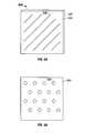
- the non-active surface 404is provided with a number of parallel grooves 406 along a first dimension, and a second number of parallel grooves 408 formed along a second dimension such that grooves 406 and 408 are orthogonal to each other, thus forming a square “cross-hatch” pattern on the non-active surface 404 of the semiconductor die 400 .
- This type of cross-hatch patternis particularly useful when the grooves 406 and 408 are cut with a wafer saw.
- numerous other patternsare useful in other embodiments of the invention which also serve to create the desired additional surface area on the non-active side of the semiconductor die.
- FIG. 5Ashows a semiconductor die 500 according to a further embodiment of the invention.
- the die 500has an active surface 502 and a non-active surface 504 .
- a plurality of parallel lines 506are formed in the non-active surface 504 of the die 500 .
- the grooves 506are disposed parallel to each other and diagonally across the non-active surface 504 of the die 500 .
- grooves 506do not run from edge to edge of the die 500 , but rather, are contained within the non-active surface 504 of the die 500 .
- the groovesare also extendible to the edges of the die 500 , or may be oriented in different directions relative to the die 500 as a matter of design choice.
- FIG. 5Bshows still a further embodiment of the invention which the non-active surface 504 is etched with a plurality of “holes” 508 which are sufficiently large enough to allow inflow of the attachment epoxy when the semiconductor die is attached to the heat sink.
- holes 508could be formed by etching processes known to those of skill in the art. Numerous other suitable grooves, shapes and configurations will occur to those of skill in the art which provide the desired increase in adhesive contact surface area on the non-active side of the semiconductor die.
- FIG. 6shows a cross-sectional view of a portion of a semiconductor die 602 having grooves 608 , 610 and 612 formed therein.
- the die 602has an active surface 606 and a non-active surface 604 .
- the active surface 606 of die 602has the active circuit elements, such as transistors, capacitors and bond pads formed thereon.
- active circuit elementssuch as transistors, capacitors and bond pads formed thereon.
- many of the active circuit elements formed on the active surface 606extend into the silicon of the semiconductor device 602 for various depths which depend on the circuit elements, and the process technology.
- there is effectively a region 622which extends a distance into the silicon material below the active surface 606 which can not be disturbed without risk to the circuit elements. This limits the depth to which the grooves 608 , 610 and 612 may be cut into the non-active surface of the die 600 without disturbing the circuit elements.
- the depth 616 of the groovesit is useful to limit the depth 616 of the grooves to about one-half the thickness of the die 602 . This generally ensures the die will not be damaged. Greater depths are permissible, as long as the groove 608 does not penetrate into the region 622 containing the active circuit elements. According to an even more specific embodiment of the invention, for a die 602 having a thickness of between about 13 and about 17 mils, the depth 616 of the grooves 608 , 610 and 612 is between about 5 and about 8 mils.
- the width 618 of the groovesis variable as a matter of design choice, but generally, since it is normally desirable to increase the surface area exposed to the adhesive, the width may be advantageously limited to about twice the depth. In one embodiment, the width of the grooves is between about 1.5 to 2 times the depth 616 of the grooves. In still another embodiment of the invention, it is advantageous that the minimum width of the grooves 608 , 610 and 612 is about the same, i.e., one-to-one ratio, as the depth 616 .
- the number of grooves provided on the non-active side 604 of the die 602is also a matter of design choice, but typically, the greatest practical number of grooves is preferred because each groove increases the surface area available for contact with the attachment adhesive.
- the number of grooves on the dieis controlled by varying the distance 614 between each groove.
- the spacing dimension 614is about one-half of the width of the groove 608 .
- the spacing distance 614would be 1 millimeter.
- the bottom portion of the groovesis provided with a rounded curvature.
- the bottom portion of groove 608is rounded with a curvature 620 .
- Thisis advantageous over a groove having a flat bottom, for example groove 612 , because the curvature 620 serves to relieve corner stress at the junction of the bottom and sides of the groove 612 which can result in fracturing of the semiconductor die 602 during the thermal stress caused by temperature cycling of the die 602 during operation, as shown with reference to groove 612 .
- the precise radius of the curvature 620is not critical and may be determined as a matter of design choice depending on the process used to form the grooves.
- the curvaturecorresponds to the radius of curvature of the diamond coated saw blade if the grooves are cut with a wafer saw. If the grooves are etched, then care must be taken to be sure that a proper curvature 620 is formed.
Landscapes
- Cooling Or The Like Of Semiconductors Or Solid State Devices (AREA)
- Die Bonding (AREA)
Abstract
Description
Claims (16)
Priority Applications (3)
| Application Number | Priority Date | Filing Date | Title |
|---|---|---|---|
| US08/869,796US6225695B1 (en) | 1997-06-05 | 1997-06-05 | Grooved semiconductor die for flip-chip heat sink attachment |
| EP98109931AEP0883192A2 (en) | 1997-06-05 | 1998-05-30 | Grooved semiconductor die for flip-chip sink attachment |
| JP10157238AJPH1174431A (en) | 1997-06-05 | 1998-06-05 | Semiconductor die with groove for mounting flip chip heat sink |
Applications Claiming Priority (1)
| Application Number | Priority Date | Filing Date | Title |
|---|---|---|---|
| US08/869,796US6225695B1 (en) | 1997-06-05 | 1997-06-05 | Grooved semiconductor die for flip-chip heat sink attachment |
Publications (1)
| Publication Number | Publication Date |
|---|---|
| US6225695B1true US6225695B1 (en) | 2001-05-01 |
Family
ID=25354283
Family Applications (1)
| Application Number | Title | Priority Date | Filing Date |
|---|---|---|---|
| US08/869,796Expired - LifetimeUS6225695B1 (en) | 1997-06-05 | 1997-06-05 | Grooved semiconductor die for flip-chip heat sink attachment |
Country Status (3)
| Country | Link |
|---|---|
| US (1) | US6225695B1 (en) |
| EP (1) | EP0883192A2 (en) |
| JP (1) | JPH1174431A (en) |
Cited By (63)
| Publication number | Priority date | Publication date | Assignee | Title |
|---|---|---|---|---|
| US6380621B1 (en)* | 1996-05-20 | 2002-04-30 | Hitachi, Ltd. | Semiconductor device and manufacturing method thereof |
| US6479889B1 (en)* | 1998-09-04 | 2002-11-12 | Sony Corporation | Semiconductor device package, and fabrication method thereof |
| US20020181218A1 (en)* | 2001-05-31 | 2002-12-05 | Harry Hedler | Electronic structure |
| US20030064542A1 (en)* | 2001-10-02 | 2003-04-03 | Corisis David J. | Methods of packaging an integrated circuit |
| US6552267B2 (en)* | 2001-08-13 | 2003-04-22 | Taiwan Semiconductor Manufacturing Co., Ltd. | Microelectronic assembly with stiffening member |
| US6556454B1 (en)* | 2000-10-31 | 2003-04-29 | Agilent Technologies, Inc. | High density contact arrangement |
| US20040036163A1 (en)* | 2002-08-22 | 2004-02-26 | Intel Corporation | Multi-die semiconductor package |
| US20040155360A1 (en)* | 1999-09-02 | 2004-08-12 | Salman Akram | Board-on-chip packages |
| US20040169272A1 (en)* | 1998-09-03 | 2004-09-02 | Hembree David R. | Chip on board with heat sink attachment and assembly |
| US20040188831A1 (en)* | 2003-03-27 | 2004-09-30 | Siliconware Precision Industries, Ltd. | Semiconductor package with heat spreader |
| US20040207060A1 (en)* | 1999-02-19 | 2004-10-21 | Corisis David J. | Integrated circuit packages, ball-grid array integrated circuit packages and methods of packaging an integrated circuit |
| US20040214373A1 (en)* | 2003-04-22 | 2004-10-28 | Tongbi Jiang | Packaged microelectronic devices and methods for packaging microelectronic devices |
| US20040212080A1 (en)* | 2003-04-22 | 2004-10-28 | Kai-Chi Chen | [chip package structure and process for fabricating the same] |
| US20040262746A1 (en)* | 2003-06-28 | 2004-12-30 | Samsung Electro-Mechanics Co., Ltd. | High-density chip scale package and method of manufacturing the same |
| US20050098900A1 (en)* | 2003-06-13 | 2005-05-12 | Delphi Technologies, Inc. | Relaxed tolerance flip chip assembly |
| US20050127500A1 (en)* | 2003-12-10 | 2005-06-16 | International Business Machines Corporation | Local reduction of compliant thermally conductive material layer thickness on chips |
| US20050151272A1 (en)* | 2004-01-06 | 2005-07-14 | Street Bret K. | Die package having an adhesive flow restriction area |
| US20050189568A1 (en)* | 2004-02-27 | 2005-09-01 | International Business Machines Corporation | Apparatus and methods for cooling semiconductor integrated circuit package structures |
| US20050199995A1 (en)* | 2004-03-15 | 2005-09-15 | Kentaro Nomoto | Semiconductor element and wafer level chip size package therefor |
| US20050212112A1 (en)* | 2004-03-29 | 2005-09-29 | Intel Corporation | Semiconducting device with folded interposer |
| US20050224943A1 (en)* | 2004-03-31 | 2005-10-13 | Sahaida Scott R | Semiconducting device with stacked dice |
| US20050285254A1 (en)* | 2004-06-23 | 2005-12-29 | Buot Joan R V | Semiconducting device having stacked dice |
| US20060038283A1 (en)* | 2004-08-18 | 2006-02-23 | Advanced Micro Devices, Inc. | Integrated circuit with increased heat transfer |
| US20060043581A1 (en)* | 2004-09-01 | 2006-03-02 | Victor Prokofiev | IC package with power and singal lines on opposing sides |
| US20060081979A1 (en)* | 2004-10-15 | 2006-04-20 | International Business Machines Corporation | Thermal properties for microelectronic devices |
| US20070166878A1 (en)* | 2006-01-16 | 2007-07-19 | Chiu-Feng Li | Package structure and method for fabricating the same |
| US20080061451A1 (en)* | 2006-09-11 | 2008-03-13 | Siliconware Precision Industries Co., Ltd. | Semiconductor package and fabrication method thereof |
| WO2008032944A1 (en)* | 2006-09-11 | 2008-03-20 | Nepes Corporation | Flip chip semiconductor package and fabrication method thereof |
| US20080106868A1 (en)* | 2006-11-03 | 2008-05-08 | Dell Products L.P. | Thermal interface material volume between thermal conducting members |
| US20080273312A1 (en)* | 2007-05-04 | 2008-11-06 | Henry Descalzo Bathan | Integrated circuit package system with interference-fit feature |
| US20080290514A1 (en)* | 2007-05-21 | 2008-11-27 | Samsung Electronics Co., Ltd. | Semiconductor device package and method of fabricating the same |
| US20090072383A1 (en)* | 2006-05-26 | 2009-03-19 | Murata Manufacturing Co., Ltd. | Semiconductor device, electronic component module, and method for manufacturing semiconductor device |
| US20100032161A1 (en)* | 2008-08-05 | 2010-02-11 | Baker Hughes Incorporated | Heat dissipater for electronic components in downhole tools and methods for using the same |
| US20100066631A1 (en)* | 2006-09-21 | 2010-03-18 | Raytheon Company | Panel Array |
| US20100126010A1 (en)* | 2006-09-21 | 2010-05-27 | Raytheon Company | Radio Frequency Interconnect Circuits and Techniques |
| US20100245179A1 (en)* | 2009-03-24 | 2010-09-30 | Raytheon Company | Method and Apparatus for Thermal Management of a Radio Frequency System |
| US20100246133A1 (en)* | 2009-03-31 | 2010-09-30 | Apple Inc. | Method and apparatus for distributing a thermal interface material |
| US7906857B1 (en) | 2008-03-13 | 2011-03-15 | Xilinx, Inc. | Molded integrated circuit package and method of forming a molded integrated circuit package |
| US20110075377A1 (en)* | 2009-09-25 | 2011-03-31 | Raytheon Copany | Heat Sink Interface Having Three-Dimensional Tolerance Compensation |
| US20110316162A1 (en)* | 2010-06-24 | 2011-12-29 | Ko Wonjun | Integrated circuit packaging system with trenches and method of manufacture thereof |
| US20120241941A1 (en)* | 2011-03-21 | 2012-09-27 | Stats Chippac, Ltd. | Semiconductor Device and Method of Forming a Thermally Reinforced Semiconductor Die |
| US8355255B2 (en) | 2010-12-22 | 2013-01-15 | Raytheon Company | Cooling of coplanar active circuits |
| US8362609B1 (en) | 2009-10-27 | 2013-01-29 | Xilinx, Inc. | Integrated circuit package and method of forming an integrated circuit package |
| US8363413B2 (en) | 2010-09-13 | 2013-01-29 | Raytheon Company | Assembly to provide thermal cooling |
| US8427371B2 (en) | 2010-04-09 | 2013-04-23 | Raytheon Company | RF feed network for modular active aperture electronically steered arrays |
| US8508943B2 (en) | 2009-10-16 | 2013-08-13 | Raytheon Company | Cooling active circuits |
| US20130315720A1 (en)* | 2012-05-22 | 2013-11-28 | Valeo Systemes De Controle Moteur | Electrical compressor housing comprising a dissipation device, and compressor including such a housing |
| US8810448B1 (en) | 2010-11-18 | 2014-08-19 | Raytheon Company | Modular architecture for scalable phased array radars |
| US8810028B1 (en) | 2010-06-30 | 2014-08-19 | Xilinx, Inc. | Integrated circuit packaging devices and methods |
| US8921990B2 (en) | 2012-12-18 | 2014-12-30 | Samsung Electronics Co., Ltd. | Semiconductor package |
| US9019166B2 (en) | 2009-06-15 | 2015-04-28 | Raytheon Company | Active electronically scanned array (AESA) card |
| US9124361B2 (en) | 2011-10-06 | 2015-09-01 | Raytheon Company | Scalable, analog monopulse network |
| US9172145B2 (en) | 2006-09-21 | 2015-10-27 | Raytheon Company | Transmit/receive daughter card with integral circulator |
| US9281228B2 (en) | 2011-11-01 | 2016-03-08 | Stats Chippac, Ltd. | Semiconductor device and method of forming thermal interface material and heat spreader over semiconductor die |
| US9431316B2 (en) | 2010-05-04 | 2016-08-30 | STATS ChipPAC Pte. Ltd. | Semiconductor device and method of forming channels in back surface of FO-WLCSP for heat dissipation |
| US20180076113A1 (en)* | 2016-09-15 | 2018-03-15 | International Business Machines Corporation | Chip package for two-phase cooling and assembly process thereof |
| US9991187B2 (en) | 2013-01-18 | 2018-06-05 | Fujitsu Limited | Electronic device and method for manufacturing the same, and substrate structure and method for manufacturing the same |
| CN110828539A (en)* | 2018-08-10 | 2020-02-21 | 北京嘉楠捷思信息技术有限公司 | A chip package structure |
| CN111554586A (en)* | 2020-06-12 | 2020-08-18 | 厦门通富微电子有限公司 | Preparation method of chip packaging body |
| CN113517243A (en)* | 2021-06-29 | 2021-10-19 | 北京时代民芯科技有限公司 | A non-hermetic ceramic flip-chip package heat dissipation structure |
| US20220208638A1 (en)* | 2019-06-24 | 2022-06-30 | Amkor Technology Singapore Holding Pte. Ltd. | Semiconductor device and method of manufacturing a semiconductor device |
| US20220230937A1 (en)* | 2021-01-20 | 2022-07-21 | Jetcool Technologies Inc. | Conformal Cooling Assembly with Substrate Fluid-Proofing for Multi-Die Electronic Assemblies |
| US20240014082A1 (en)* | 2022-07-06 | 2024-01-11 | United Microelectronics Corp. | Semiconductor structure and manufacturing method thereof |
Families Citing this family (11)
| Publication number | Priority date | Publication date | Assignee | Title |
|---|---|---|---|---|
| KR100565962B1 (en)* | 2000-01-06 | 2006-03-30 | 삼성전자주식회사 | Fiji Packages with Flip Chip Technology |
| US6467878B1 (en)* | 2000-05-10 | 2002-10-22 | Hewlett-Packard Company | System and method for locally controlling the thickness of a flexible nozzle member |
| DE10030443A1 (en)* | 2000-06-22 | 2002-01-17 | Infineon Technologies Ag | Production of a heat deviating surface of a component used in the production of a semiconductor element comprises inserting trenches into the component using an etching process |
| KR100442695B1 (en)* | 2001-09-10 | 2004-08-02 | 삼성전자주식회사 | Method for manufacturing flip chip package devices with heat spreaders |
| AU2003266358A1 (en)* | 2002-10-16 | 2004-05-04 | Sew-Eurodrive Gmbh And Co | Device |
| JP5251073B2 (en)* | 2007-03-08 | 2013-07-31 | 日産自動車株式会社 | Semiconductor device and manufacturing method thereof |
| EP1968109A3 (en) | 2007-03-08 | 2012-08-01 | Nissan Motor Co., Ltd. | Semiconductor device and method of manufacturing the same |
| KR100855624B1 (en) | 2007-06-01 | 2008-09-03 | 삼성전기주식회사 | Semiconductor package and manufacturing method |
| JP6560496B2 (en)* | 2015-01-26 | 2019-08-14 | 株式会社ジェイデバイス | Semiconductor device |
| FR3061600B1 (en)* | 2017-01-03 | 2020-06-26 | Stmicroelectronics (Grenoble 2) Sas | ELECTRONIC DEVICE COMPRISING A GROOVED CHIP |
| JP2024133776A (en)* | 2023-03-20 | 2024-10-03 | ソニーセミコンダクタソリューションズ株式会社 | Semiconductor Device |
Citations (6)
| Publication number | Priority date | Publication date | Assignee | Title |
|---|---|---|---|---|
| JPS5821347A (en)* | 1981-07-29 | 1983-02-08 | Toshiba Corp | Flat type semiconductor device |
| US5223747A (en)* | 1990-06-15 | 1993-06-29 | Battelle-Institut E.V. | Heat dissipating device |
| US5387815A (en)* | 1991-07-12 | 1995-02-07 | Sumitomo Electric Industries, Ltd. | Semiconductor chip module |
| US5514906A (en)* | 1993-11-10 | 1996-05-07 | Fujitsu Limited | Apparatus for cooling semiconductor chips in multichip modules |
| US5644586A (en)* | 1994-09-16 | 1997-07-01 | Mitsubishi Denki Kabushiki Kaisha | Semiconductor laser device and method of fabricating semiconductor laser device |
| US5770478A (en)* | 1996-12-03 | 1998-06-23 | International Business Machines Corporation | Integral mesh flat plate cooling method |
- 1997
- 1997-06-05USUS08/869,796patent/US6225695B1/ennot_activeExpired - Lifetime
- 1998
- 1998-05-30EPEP98109931Apatent/EP0883192A2/ennot_activeWithdrawn
- 1998-06-05JPJP10157238Apatent/JPH1174431A/enactivePending
Patent Citations (6)
| Publication number | Priority date | Publication date | Assignee | Title |
|---|---|---|---|---|
| JPS5821347A (en)* | 1981-07-29 | 1983-02-08 | Toshiba Corp | Flat type semiconductor device |
| US5223747A (en)* | 1990-06-15 | 1993-06-29 | Battelle-Institut E.V. | Heat dissipating device |
| US5387815A (en)* | 1991-07-12 | 1995-02-07 | Sumitomo Electric Industries, Ltd. | Semiconductor chip module |
| US5514906A (en)* | 1993-11-10 | 1996-05-07 | Fujitsu Limited | Apparatus for cooling semiconductor chips in multichip modules |
| US5644586A (en)* | 1994-09-16 | 1997-07-01 | Mitsubishi Denki Kabushiki Kaisha | Semiconductor laser device and method of fabricating semiconductor laser device |
| US5770478A (en)* | 1996-12-03 | 1998-06-23 | International Business Machines Corporation | Integral mesh flat plate cooling method |
Cited By (122)
| Publication number | Priority date | Publication date | Assignee | Title |
|---|---|---|---|---|
| US6380621B1 (en)* | 1996-05-20 | 2002-04-30 | Hitachi, Ltd. | Semiconductor device and manufacturing method thereof |
| US20040169272A1 (en)* | 1998-09-03 | 2004-09-02 | Hembree David R. | Chip on board with heat sink attachment and assembly |
| US7244637B2 (en) | 1998-09-03 | 2007-07-17 | Micron Technology, Inc. | Chip on board and heat sink attachment methods |
| US6777792B2 (en) | 1998-09-04 | 2004-08-17 | Hiroshi Yoshida | Semiconductor device and package with high heat radiation effect |
| US6479889B1 (en)* | 1998-09-04 | 2002-11-12 | Sony Corporation | Semiconductor device package, and fabrication method thereof |
| US20040207060A1 (en)* | 1999-02-19 | 2004-10-21 | Corisis David J. | Integrated circuit packages, ball-grid array integrated circuit packages and methods of packaging an integrated circuit |
| US6856013B1 (en)* | 1999-02-19 | 2005-02-15 | Micron Technology, Inc. | Integrated circuit packages, ball-grid array integrated circuit packages and methods of packaging an integrated circuit |
| US6939739B2 (en) | 1999-02-19 | 2005-09-06 | Micron Technology, Inc. | Integrated circuit packages, ball-grid array integrated circuit packages and methods of packaging an integrated circuit |
| US6917107B2 (en) | 1999-09-02 | 2005-07-12 | Micron Technology, Inc. | Board-on-chip packages |
| US6900077B2 (en) | 1999-09-02 | 2005-05-31 | Micron Technology, Inc. | Methods of forming board-on-chip packages |
| US7443022B2 (en) | 1999-09-02 | 2008-10-28 | Micron Technology, Inc. | Board-on-chip packages |
| US6825550B2 (en) | 1999-09-02 | 2004-11-30 | Micron Technology, Inc. | Board-on-chip packages with conductive foil on the chip surface |
| US20040155360A1 (en)* | 1999-09-02 | 2004-08-12 | Salman Akram | Board-on-chip packages |
| US6556454B1 (en)* | 2000-10-31 | 2003-04-29 | Agilent Technologies, Inc. | High density contact arrangement |
| US20020181218A1 (en)* | 2001-05-31 | 2002-12-05 | Harry Hedler | Electronic structure |
| US6826037B2 (en)* | 2001-05-31 | 2004-11-30 | Infineon Technologies Ag | Electronic structure |
| US6552267B2 (en)* | 2001-08-13 | 2003-04-22 | Taiwan Semiconductor Manufacturing Co., Ltd. | Microelectronic assembly with stiffening member |
| US20030064542A1 (en)* | 2001-10-02 | 2003-04-03 | Corisis David J. | Methods of packaging an integrated circuit |
| US20040036163A1 (en)* | 2002-08-22 | 2004-02-26 | Intel Corporation | Multi-die semiconductor package |
| US7498201B2 (en) | 2002-08-22 | 2009-03-03 | Intel Corporation | Method of forming a multi-die semiconductor package |
| US20050233497A1 (en)* | 2002-08-22 | 2005-10-20 | Intel Corporation | Method of forming a multi-die semiconductor package |
| US6927497B2 (en)* | 2002-08-22 | 2005-08-09 | Intel Corporation | Multi-die semiconductor package |
| US20040188831A1 (en)* | 2003-03-27 | 2004-09-30 | Siliconware Precision Industries, Ltd. | Semiconductor package with heat spreader |
| US6919630B2 (en)* | 2003-03-27 | 2005-07-19 | Siliconware Precision Industries Co. Ltd. | Semiconductor package with heat spreader |
| US20060030150A1 (en)* | 2003-04-22 | 2006-02-09 | Micron Technology, Inc. | Packaged microelectronic devices and methods for packaging microelectronic devices |
| US20080099917A1 (en)* | 2003-04-22 | 2008-05-01 | Micron Technology, Inc. | Packaged microelectronic devices and methods for packaging microelectronic devices |
| US7312101B2 (en) | 2003-04-22 | 2007-12-25 | Micron Technology, Inc. | Packaged microelectronic devices and methods for packaging microelectronic devices |
| US20040214373A1 (en)* | 2003-04-22 | 2004-10-28 | Tongbi Jiang | Packaged microelectronic devices and methods for packaging microelectronic devices |
| US7329949B2 (en)* | 2003-04-22 | 2008-02-12 | Micron Technology, Inc. | Packaged microelectronic devices and methods for packaging microelectronic devices |
| US20080132006A1 (en)* | 2003-04-22 | 2008-06-05 | Micron Technology, Inc. | Packaged microelectronic devices and methods for packaging microelectronic devices |
| US7655500B2 (en) | 2003-04-22 | 2010-02-02 | Micron Technology | Packaged microelectronic devices and methods for packaging microelectronic devices |
| US20040212080A1 (en)* | 2003-04-22 | 2004-10-28 | Kai-Chi Chen | [chip package structure and process for fabricating the same] |
| US7550847B2 (en) | 2003-04-22 | 2009-06-23 | Micron Technology, Inc. | Packaged microelectronic devices and methods for packaging microelectronic devices |
| US20050098900A1 (en)* | 2003-06-13 | 2005-05-12 | Delphi Technologies, Inc. | Relaxed tolerance flip chip assembly |
| US20040262746A1 (en)* | 2003-06-28 | 2004-12-30 | Samsung Electro-Mechanics Co., Ltd. | High-density chip scale package and method of manufacturing the same |
| US20050127500A1 (en)* | 2003-12-10 | 2005-06-16 | International Business Machines Corporation | Local reduction of compliant thermally conductive material layer thickness on chips |
| US7491570B2 (en)* | 2004-01-06 | 2009-02-17 | Micron Technology, Inc. | Die package having an adhesive flow restriction area |
| US7476955B2 (en)* | 2004-01-06 | 2009-01-13 | Micron Technology, Inc. | Die package having an adhesive flow restriction area |
| US20050156266A1 (en)* | 2004-01-06 | 2005-07-21 | Street Bret K. | Die package having an adhesive flow restriction area |
| US20070114646A1 (en)* | 2004-01-06 | 2007-05-24 | Street Bret K | Die package having an adhesive flow restriction area |
| US20050151272A1 (en)* | 2004-01-06 | 2005-07-14 | Street Bret K. | Die package having an adhesive flow restriction area |
| US7288839B2 (en) | 2004-02-27 | 2007-10-30 | International Business Machines Corporation | Apparatus and methods for cooling semiconductor integrated circuit package structures |
| US20050189568A1 (en)* | 2004-02-27 | 2005-09-01 | International Business Machines Corporation | Apparatus and methods for cooling semiconductor integrated circuit package structures |
| US7830011B2 (en) | 2004-03-15 | 2010-11-09 | Yamaha Corporation | Semiconductor element and wafer level chip size package therefor |
| US20050199995A1 (en)* | 2004-03-15 | 2005-09-15 | Kentaro Nomoto | Semiconductor element and wafer level chip size package therefor |
| US7482698B2 (en) | 2004-03-29 | 2009-01-27 | Intel Corporation | Semiconducting device with folded interposer |
| US7456048B2 (en) | 2004-03-29 | 2008-11-25 | Intel Corporation | Semiconducting device with folded interposer |
| US7145249B2 (en) | 2004-03-29 | 2006-12-05 | Intel Corporation | Semiconducting device with folded interposer |
| US20070023905A1 (en)* | 2004-03-29 | 2007-02-01 | Intel Corporation | Semiconducting device with folded interposer |
| US20070026569A1 (en)* | 2004-03-29 | 2007-02-01 | Intel Corporation | Semiconducting device with folded interposer |
| US20050212112A1 (en)* | 2004-03-29 | 2005-09-29 | Intel Corporation | Semiconducting device with folded interposer |
| US7378725B2 (en) | 2004-03-31 | 2008-05-27 | Intel Corporation | Semiconducting device with stacked dice |
| US20050224943A1 (en)* | 2004-03-31 | 2005-10-13 | Sahaida Scott R | Semiconducting device with stacked dice |
| US20050285254A1 (en)* | 2004-06-23 | 2005-12-29 | Buot Joan R V | Semiconducting device having stacked dice |
| TWI416675B (en)* | 2004-08-18 | 2013-11-21 | Globalfoundries Us Inc | Integrated circuit with increased heat conduction |
| US7259458B2 (en) | 2004-08-18 | 2007-08-21 | Advanced Micro Devices, Inc. | Integrated circuit with increased heat transfer |
| WO2006022911A1 (en)* | 2004-08-18 | 2006-03-02 | Advanced Micro Devices, Inc. | Integrated circuit with increased heat transfer |
| US20060038283A1 (en)* | 2004-08-18 | 2006-02-23 | Advanced Micro Devices, Inc. | Integrated circuit with increased heat transfer |
| US7235880B2 (en)* | 2004-09-01 | 2007-06-26 | Intel Corporation | IC package with power and signal lines on opposing sides |
| US20060043581A1 (en)* | 2004-09-01 | 2006-03-02 | Victor Prokofiev | IC package with power and singal lines on opposing sides |
| US7329948B2 (en)* | 2004-10-15 | 2008-02-12 | International Business Machines Corporation | Microelectronic devices and methods |
| US20060081979A1 (en)* | 2004-10-15 | 2006-04-20 | International Business Machines Corporation | Thermal properties for microelectronic devices |
| US20070166878A1 (en)* | 2006-01-16 | 2007-07-19 | Chiu-Feng Li | Package structure and method for fabricating the same |
| US7928559B2 (en) | 2006-05-26 | 2011-04-19 | Murata Manufacturing Co., Ltd. | Semiconductor device, electronic component module, and method for manufacturing semiconductor device |
| US20090072383A1 (en)* | 2006-05-26 | 2009-03-19 | Murata Manufacturing Co., Ltd. | Semiconductor device, electronic component module, and method for manufacturing semiconductor device |
| US8895366B2 (en) | 2006-09-11 | 2014-11-25 | Siliconware Precision Industries Co., Ltd. | Fabrication method of semiconductor package |
| US8698326B2 (en) | 2006-09-11 | 2014-04-15 | Silconware Precision Industries Co., Ltd. | Semiconductor package and fabrication method thereof |
| WO2008032944A1 (en)* | 2006-09-11 | 2008-03-20 | Nepes Corporation | Flip chip semiconductor package and fabrication method thereof |
| US20080061451A1 (en)* | 2006-09-11 | 2008-03-13 | Siliconware Precision Industries Co., Ltd. | Semiconductor package and fabrication method thereof |
| US8093721B2 (en) | 2006-09-11 | 2012-01-10 | Nepes Corporation | Flip chip semiconductor package and fabrication method thereof |
| US20100066631A1 (en)* | 2006-09-21 | 2010-03-18 | Raytheon Company | Panel Array |
| US20100126010A1 (en)* | 2006-09-21 | 2010-05-27 | Raytheon Company | Radio Frequency Interconnect Circuits and Techniques |
| US8981869B2 (en) | 2006-09-21 | 2015-03-17 | Raytheon Company | Radio frequency interconnect circuits and techniques |
| US8279131B2 (en) | 2006-09-21 | 2012-10-02 | Raytheon Company | Panel array |
| US9172145B2 (en) | 2006-09-21 | 2015-10-27 | Raytheon Company | Transmit/receive daughter card with integral circulator |
| US20080106868A1 (en)* | 2006-11-03 | 2008-05-08 | Dell Products L.P. | Thermal interface material volume between thermal conducting members |
| US20080273312A1 (en)* | 2007-05-04 | 2008-11-06 | Henry Descalzo Bathan | Integrated circuit package system with interference-fit feature |
| US7977778B2 (en)* | 2007-05-04 | 2011-07-12 | Stats Chippac Ltd. | Integrated circuit package system with interference-fit feature |
| US20080290514A1 (en)* | 2007-05-21 | 2008-11-27 | Samsung Electronics Co., Ltd. | Semiconductor device package and method of fabricating the same |
| US7906857B1 (en) | 2008-03-13 | 2011-03-15 | Xilinx, Inc. | Molded integrated circuit package and method of forming a molded integrated circuit package |
| US20100032161A1 (en)* | 2008-08-05 | 2010-02-11 | Baker Hughes Incorporated | Heat dissipater for electronic components in downhole tools and methods for using the same |
| US8763702B2 (en)* | 2008-08-05 | 2014-07-01 | Baker Hughes Incorporated | Heat dissipater for electronic components in downhole tools and methods for using the same |
| US7859835B2 (en) | 2009-03-24 | 2010-12-28 | Allegro Microsystems, Inc. | Method and apparatus for thermal management of a radio frequency system |
| US20100245179A1 (en)* | 2009-03-24 | 2010-09-30 | Raytheon Company | Method and Apparatus for Thermal Management of a Radio Frequency System |
| US7961469B2 (en)* | 2009-03-31 | 2011-06-14 | Apple Inc. | Method and apparatus for distributing a thermal interface material |
| US20100246133A1 (en)* | 2009-03-31 | 2010-09-30 | Apple Inc. | Method and apparatus for distributing a thermal interface material |
| US20110228482A1 (en)* | 2009-03-31 | 2011-09-22 | Apple Inc. | Method and apparatus for distributing a thermal interface material |
| US8564955B2 (en) | 2009-03-31 | 2013-10-22 | Apple Inc. | Coupling heat sink to integrated circuit chip with thermal interface material |
| US9019166B2 (en) | 2009-06-15 | 2015-04-28 | Raytheon Company | Active electronically scanned array (AESA) card |
| US20110075377A1 (en)* | 2009-09-25 | 2011-03-31 | Raytheon Copany | Heat Sink Interface Having Three-Dimensional Tolerance Compensation |
| US8537552B2 (en) | 2009-09-25 | 2013-09-17 | Raytheon Company | Heat sink interface having three-dimensional tolerance compensation |
| US8508943B2 (en) | 2009-10-16 | 2013-08-13 | Raytheon Company | Cooling active circuits |
| US8362609B1 (en) | 2009-10-27 | 2013-01-29 | Xilinx, Inc. | Integrated circuit package and method of forming an integrated circuit package |
| US8427371B2 (en) | 2010-04-09 | 2013-04-23 | Raytheon Company | RF feed network for modular active aperture electronically steered arrays |
| US9431316B2 (en) | 2010-05-04 | 2016-08-30 | STATS ChipPAC Pte. Ltd. | Semiconductor device and method of forming channels in back surface of FO-WLCSP for heat dissipation |
| US8536718B2 (en)* | 2010-06-24 | 2013-09-17 | Stats Chippac Ltd. | Integrated circuit packaging system with trenches and method of manufacture thereof |
| US20110316162A1 (en)* | 2010-06-24 | 2011-12-29 | Ko Wonjun | Integrated circuit packaging system with trenches and method of manufacture thereof |
| US8810028B1 (en) | 2010-06-30 | 2014-08-19 | Xilinx, Inc. | Integrated circuit packaging devices and methods |
| US8363413B2 (en) | 2010-09-13 | 2013-01-29 | Raytheon Company | Assembly to provide thermal cooling |
| US9116222B1 (en) | 2010-11-18 | 2015-08-25 | Raytheon Company | Modular architecture for scalable phased array radars |
| US8810448B1 (en) | 2010-11-18 | 2014-08-19 | Raytheon Company | Modular architecture for scalable phased array radars |
| US8355255B2 (en) | 2010-12-22 | 2013-01-15 | Raytheon Company | Cooling of coplanar active circuits |
| US8786076B2 (en)* | 2011-03-21 | 2014-07-22 | Stats Chippac, Ltd. | Semiconductor device and method of forming a thermally reinforced semiconductor die |
| US20120241941A1 (en)* | 2011-03-21 | 2012-09-27 | Stats Chippac, Ltd. | Semiconductor Device and Method of Forming a Thermally Reinforced Semiconductor Die |
| US9124361B2 (en) | 2011-10-06 | 2015-09-01 | Raytheon Company | Scalable, analog monopulse network |
| US9397766B2 (en) | 2011-10-06 | 2016-07-19 | Raytheon Company | Calibration system and technique for a scalable, analog monopulse network |
| US9281228B2 (en) | 2011-11-01 | 2016-03-08 | Stats Chippac, Ltd. | Semiconductor device and method of forming thermal interface material and heat spreader over semiconductor die |
| US20130315720A1 (en)* | 2012-05-22 | 2013-11-28 | Valeo Systemes De Controle Moteur | Electrical compressor housing comprising a dissipation device, and compressor including such a housing |
| US9293389B2 (en) | 2012-12-18 | 2016-03-22 | Samsung Electronics Co., Ltd. | Method of manufacturing a semiconductor package including a surface profile modifier |
| US8921990B2 (en) | 2012-12-18 | 2014-12-30 | Samsung Electronics Co., Ltd. | Semiconductor package |
| US9991187B2 (en) | 2013-01-18 | 2018-06-05 | Fujitsu Limited | Electronic device and method for manufacturing the same, and substrate structure and method for manufacturing the same |
| US20180076113A1 (en)* | 2016-09-15 | 2018-03-15 | International Business Machines Corporation | Chip package for two-phase cooling and assembly process thereof |
| US10607963B2 (en)* | 2016-09-15 | 2020-03-31 | International Business Machines Corporation | Chip package for two-phase cooling and assembly process thereof |
| CN110828539A (en)* | 2018-08-10 | 2020-02-21 | 北京嘉楠捷思信息技术有限公司 | A chip package structure |
| US12021005B2 (en)* | 2019-06-24 | 2024-06-25 | Amkor Technology Singapore Holding Pte. Ltd. | Semiconductor device including a thermal material |
| US20220208638A1 (en)* | 2019-06-24 | 2022-06-30 | Amkor Technology Singapore Holding Pte. Ltd. | Semiconductor device and method of manufacturing a semiconductor device |
| CN111554586A (en)* | 2020-06-12 | 2020-08-18 | 厦门通富微电子有限公司 | Preparation method of chip packaging body |
| CN111554586B (en)* | 2020-06-12 | 2022-04-01 | 厦门通富微电子有限公司 | Preparation method of chip packaging body |
| US20220230937A1 (en)* | 2021-01-20 | 2022-07-21 | Jetcool Technologies Inc. | Conformal Cooling Assembly with Substrate Fluid-Proofing for Multi-Die Electronic Assemblies |
| US12288733B2 (en)* | 2021-01-20 | 2025-04-29 | Jetcool Technologies Inc. | Conformal cooling assembly with substrate fluid-proofing for multi-die electronic assemblies |
| CN113517243A (en)* | 2021-06-29 | 2021-10-19 | 北京时代民芯科技有限公司 | A non-hermetic ceramic flip-chip package heat dissipation structure |
| US20240014082A1 (en)* | 2022-07-06 | 2024-01-11 | United Microelectronics Corp. | Semiconductor structure and manufacturing method thereof |
Also Published As
| Publication number | Publication date |
|---|---|
| JPH1174431A (en) | 1999-03-16 |
| EP0883192A2 (en) | 1998-12-09 |
Similar Documents
| Publication | Publication Date | Title |
|---|---|---|
| US6225695B1 (en) | Grooved semiconductor die for flip-chip heat sink attachment | |
| CN100429775C (en) | Integrated circuit packaging device and manufacturing method thereof | |
| CN100563024C (en) | Package with exposed integrated circuit device | |
| KR0156013B1 (en) | Heat sink and cover for tab integrated circuits | |
| US5940271A (en) | Stiffener with integrated heat sink attachment | |
| US6081037A (en) | Semiconductor component having a semiconductor chip mounted to a chip mount | |
| US7112882B2 (en) | Structures and methods for heat dissipation of semiconductor integrated circuits | |
| EP0054539B1 (en) | A semiconductor integrated circuit device with an improved heat sink | |
| US6700783B1 (en) | Three-dimensional stacked heat spreader assembly for electronic package and method for assembling | |
| US5525835A (en) | Semiconductor chip module having an electrically insulative thermally conductive thermal dissipator directly in contact with the semiconductor element | |
| US20060209516A1 (en) | Electronic assembly with integral thermal transient suppression | |
| US4471407A (en) | Combination heat sink for a semiconductor | |
| KR960000222B1 (en) | Semiconductor Package with Heat-Sink | |
| KR100631403B1 (en) | Semiconductor package with heat sink and manufacturing method thereof | |
| JPH02276264A (en) | Ceramic package provided with heat sink | |
| CN218957731U (en) | Package for integrated circuit | |
| KR100676315B1 (en) | High Thermal Emission Semiconductor Chip Package | |
| US20030020160A1 (en) | Semiconductor device die and package having improved heat dissipation capability | |
| JP2718203B2 (en) | Ceramic package with heat sink | |
| JP2961976B2 (en) | Semiconductor package with heat sink | |
| KR20020039010A (en) | Double die package having heat spreaders | |
| JPH0521665A (en) | Semiconductor package provided with heat sink | |
| US6498390B1 (en) | Integrated circuit package that includes a thermally conductive tape which attaches a thermal element to a plastic housing | |
| CN222233626U (en) | Chip packaging structure and electronic products | |
| JPS6219074B2 (en) |
Legal Events
| Date | Code | Title | Description |
|---|---|---|---|
| AS | Assignment | Owner name:LSI LOGIC CORPORATION, CALIFORNIA Free format text:ASSIGNMENT OF ASSIGNORS INTEREST;ASSIGNORS:CHIA, CHOK J.;LIM, SENG-SOOI;ALAGARATNAM, MANIAM;REEL/FRAME:008597/0211 Effective date:19970604 | |
| STCF | Information on status: patent grant | Free format text:PATENTED CASE | |
| FPAY | Fee payment | Year of fee payment:4 | |
| FEPP | Fee payment procedure | Free format text:PAYOR NUMBER ASSIGNED (ORIGINAL EVENT CODE: ASPN); ENTITY STATUS OF PATENT OWNER: LARGE ENTITY Free format text:PAYER NUMBER DE-ASSIGNED (ORIGINAL EVENT CODE: RMPN); ENTITY STATUS OF PATENT OWNER: LARGE ENTITY | |
| FPAY | Fee payment | Year of fee payment:8 | |
| FPAY | Fee payment | Year of fee payment:12 | |
| AS | Assignment | Owner name:DEUTSCHE BANK AG NEW YORK BRANCH, AS COLLATERAL AG Free format text:PATENT SECURITY AGREEMENT;ASSIGNORS:LSI CORPORATION;AGERE SYSTEMS LLC;REEL/FRAME:032856/0031 Effective date:20140506 | |
| AS | Assignment | Owner name:LSI CORPORATION, CALIFORNIA Free format text:CHANGE OF NAME;ASSIGNOR:LSI LOGIC CORPORATION;REEL/FRAME:033102/0270 Effective date:20070406 | |
| AS | Assignment | Owner name:AVAGO TECHNOLOGIES GENERAL IP (SINGAPORE) PTE. LTD Free format text:ASSIGNMENT OF ASSIGNORS INTEREST;ASSIGNOR:LSI CORPORATION;REEL/FRAME:035058/0248 Effective date:20140804 | |
| AS | Assignment | Owner name:LSI CORPORATION, CALIFORNIA Free format text:TERMINATION AND RELEASE OF SECURITY INTEREST IN PATENT RIGHTS (RELEASES RF 032856-0031);ASSIGNOR:DEUTSCHE BANK AG NEW YORK BRANCH, AS COLLATERAL AGENT;REEL/FRAME:037684/0039 Effective date:20160201 Owner name:AGERE SYSTEMS LLC, PENNSYLVANIA Free format text:TERMINATION AND RELEASE OF SECURITY INTEREST IN PATENT RIGHTS (RELEASES RF 032856-0031);ASSIGNOR:DEUTSCHE BANK AG NEW YORK BRANCH, AS COLLATERAL AGENT;REEL/FRAME:037684/0039 Effective date:20160201 | |
| AS | Assignment | Owner name:BANK OF AMERICA, N.A., AS COLLATERAL AGENT, NORTH CAROLINA Free format text:PATENT SECURITY AGREEMENT;ASSIGNOR:AVAGO TECHNOLOGIES GENERAL IP (SINGAPORE) PTE. LTD.;REEL/FRAME:037808/0001 Effective date:20160201 Owner name:BANK OF AMERICA, N.A., AS COLLATERAL AGENT, NORTH Free format text:PATENT SECURITY AGREEMENT;ASSIGNOR:AVAGO TECHNOLOGIES GENERAL IP (SINGAPORE) PTE. LTD.;REEL/FRAME:037808/0001 Effective date:20160201 | |
| AS | Assignment | Owner name:AVAGO TECHNOLOGIES GENERAL IP (SINGAPORE) PTE. LTD., SINGAPORE Free format text:TERMINATION AND RELEASE OF SECURITY INTEREST IN PATENTS;ASSIGNOR:BANK OF AMERICA, N.A., AS COLLATERAL AGENT;REEL/FRAME:041710/0001 Effective date:20170119 Owner name:AVAGO TECHNOLOGIES GENERAL IP (SINGAPORE) PTE. LTD Free format text:TERMINATION AND RELEASE OF SECURITY INTEREST IN PATENTS;ASSIGNOR:BANK OF AMERICA, N.A., AS COLLATERAL AGENT;REEL/FRAME:041710/0001 Effective date:20170119 | |
| AS | Assignment | Owner name:BELL SEMICONDUCTOR, LLC, ILLINOIS Free format text:ASSIGNMENT OF ASSIGNORS INTEREST;ASSIGNORS:AVAGO TECHNOLOGIES GENERAL IP (SINGAPORE) PTE. LTD.;BROADCOM CORPORATION;REEL/FRAME:044886/0766 Effective date:20171208 | |
| AS | Assignment | Owner name:CORTLAND CAPITAL MARKET SERVICES LLC, AS COLLATERA Free format text:SECURITY INTEREST;ASSIGNORS:HILCO PATENT ACQUISITION 56, LLC;BELL SEMICONDUCTOR, LLC;BELL NORTHERN RESEARCH, LLC;REEL/FRAME:045216/0020 Effective date:20180124 | |
| AS | Assignment | Owner name:BELL NORTHERN RESEARCH, LLC, ILLINOIS Free format text:RELEASE BY SECURED PARTY;ASSIGNOR:CORTLAND CAPITAL MARKET SERVICES LLC;REEL/FRAME:059723/0382 Effective date:20220401 Owner name:BELL SEMICONDUCTOR, LLC, ILLINOIS Free format text:RELEASE BY SECURED PARTY;ASSIGNOR:CORTLAND CAPITAL MARKET SERVICES LLC;REEL/FRAME:059723/0382 Effective date:20220401 Owner name:HILCO PATENT ACQUISITION 56, LLC, ILLINOIS Free format text:RELEASE BY SECURED PARTY;ASSIGNOR:CORTLAND CAPITAL MARKET SERVICES LLC;REEL/FRAME:059723/0382 Effective date:20220401 |