US6225173B1 - Recessed channel structure for manufacturing shallow source/drain extensions - Google Patents
Recessed channel structure for manufacturing shallow source/drain extensionsDownload PDFInfo
- Publication number
- US6225173B1 US6225173B1US09/187,172US18717298AUS6225173B1US 6225173 B1US6225173 B1US 6225173B1US 18717298 AUS18717298 AUS 18717298AUS 6225173 B1US6225173 B1US 6225173B1
- Authority
- US
- United States
- Prior art keywords
- gate
- drain
- source
- insulative
- spacers
- Prior art date
- Legal status (The legal status is an assumption and is not a legal conclusion. Google has not performed a legal analysis and makes no representation as to the accuracy of the status listed.)
- Expired - Lifetime
Links
Images

Classifications
- H—ELECTRICITY
- H10—SEMICONDUCTOR DEVICES; ELECTRIC SOLID-STATE DEVICES NOT OTHERWISE PROVIDED FOR
- H10D—INORGANIC ELECTRIC SEMICONDUCTOR DEVICES
- H10D64/00—Electrodes of devices having potential barriers
- H10D64/01—Manufacture or treatment
- H10D64/025—Manufacture or treatment forming recessed gates, e.g. by using local oxidation
- H10D64/027—Manufacture or treatment forming recessed gates, e.g. by using local oxidation by etching at gate locations
- H—ELECTRICITY
- H10—SEMICONDUCTOR DEVICES; ELECTRIC SOLID-STATE DEVICES NOT OTHERWISE PROVIDED FOR
- H10D—INORGANIC ELECTRIC SEMICONDUCTOR DEVICES
- H10D30/00—Field-effect transistors [FET]
- H10D30/60—Insulated-gate field-effect transistors [IGFET]
- H10D30/601—Insulated-gate field-effect transistors [IGFET] having lightly-doped drain or source extensions, e.g. LDD IGFETs or DDD IGFETs
- H10D30/608—Insulated-gate field-effect transistors [IGFET] having lightly-doped drain or source extensions, e.g. LDD IGFETs or DDD IGFETs having non-planar bodies, e.g. having recessed gate electrodes
- H—ELECTRICITY
- H10—SEMICONDUCTOR DEVICES; ELECTRIC SOLID-STATE DEVICES NOT OTHERWISE PROVIDED FOR
- H10D—INORGANIC ELECTRIC SEMICONDUCTOR DEVICES
- H10D64/00—Electrodes of devices having potential barriers
- H10D64/01—Manufacture or treatment
- H10D64/017—Manufacture or treatment using dummy gates in processes wherein at least parts of the final gates are self-aligned to the dummy gates, i.e. replacement gate processes
Definitions
- the present inventionrelates to integrated circuits and methods of manufacturing integrated circuits. More particularly, the present invention relates to a method of manufacturing integrated circuits having transistors with ultra-shallow source/drain extensions.
- Integrated circuitssuch as, ultra-large scale integrated (ULSI) circuits, can include as many as one million transistors or more.
- the ULSI circuitcan include complementary metal oxide semiconductor (CMOS) field effect transistors (FETS).
- CMOScomplementary metal oxide semiconductor
- FETSfield effect transistors
- the transistorscan include semiconductor gates disposed between drain and source regions. The drain and source regions are typically heavily doped with a P-type dopant (boron) or an N-type dopant (phosphorous).
- the drain and source regionsgenerally include a thin extension that is disposed partially underneath the gate to enhance the transistor performance.
- Shallow source and drain extensionshelp to achieve immunity to short-channel effects, which degrade transistor performance for both N-channel and P-channel transistors. Short-channel effects can cause threshold voltage roll-off and drain-induced barrier-lowering. Shallow source and drain extensions and, hence, controlling short-channel effects, are particularly important as transistors become smaller.
- the source and drain extensionsare formed by providing a transistor gate structure without sidewall spacers on a top surface of a silicon substrate.
- the silicon substrateis doped on both sides of the gate structure via a conventional doping process, such as, a diffusion process or ion implantation process. Without the sidewall spacers, the doping process introduces dopants into a thin region (i.e., just below the top surface of the substrate) to form the drain and source extensions, as well as to partially form the drain and source regions.
- silicon dioxide spacerswhich abut lateral sides of the gate structure, are provided over the source and drain extensions.
- the substrateis doped a second time to form the deeper source and drain regions.
- the source and drain extensionsare not further doped due to the blocking capability of the silicon dioxide spacer.
- transistors disposed on integrated circuitsbecome smaller, transistors with shallow and ultra-shallow source and drain extensions have become more difficult to manufacture. For example, smaller transistors should have ultra-shallow source and drain extensions (less than 30 nanometer (nm) junction depth). Forming source and drain extensions with junction depths of less than 30 nm is very difficult using conventional fabrication techniques.
- Conventional ion implantation and diffusion doping techniquesmake transistors on the IC susceptible to short-channeling effects, which result in a dopant profile tail distribution that extends deep into the substrate.
- conventional ion implantation techniqueshave difficulty maintaining shallow source and drain extensions because point defects generated in the bulk semiconductor substrate during ion implantation can cause the dopant to more easily diffuse (transient enhanced diffusion, TED). The diffusion often extends the source and drain extensions vertically into the bulk semiconductor substrate.
- the present inventionrelates to a method of manufacturing an integrated circuit.
- the methodincludes providing a plurality of gate structures between a source region and a drain region in a semiconductor substrate, each of the gate structures includes a dummy material.
- the methodalso includes removing the dummy material, thereby leaving a cavity, etching a recess in the substrate within the cavity and partially in the source region and in the drain region.
- the recessforms an ultra-shallow source extension and an ultra-shallow drain extension.
- the methodalso includes providing a doped semiconductor material, in the cavity.
- the present inventionfurther relates to a method of manufacturing an ultra-large scale integrated circuit including a plurality of field effect transistors.
- Each transistorhas a source, a drain, and a gate structure disposed between the source and the drain.
- the gate structureincludes a first gate material disposed over a gate oxide.
- the methodincludes steps of depositing an insulative material over the top surface of the semiconductor substrate and over the gate structures, removing a portion of the insulative material to expose the first gate material, removing the first gate material from the gate structures, removing the gate oxide, etching the substrate underneath the gate oxide, providing a thin gate oxide, and providing a second gate material in the gate structure.
- the methodeven further relates to a damascene gate process of forming shallow source and drain extensions.
- the processincludes steps of providing a plurality of transistors that include a source region, a drain region, and at least a portion of a gate structure on a top surface of a silicon substrate.
- the gate structureincludes a gate connector located between the source region and the drain region.
- the processfurther includes steps of removing the gate conductor from the gate structure, thereby leaving a cavity in the gate structure, and etching within the cavity to provide a recessed portion in the top surface of the substrate, thereby forming the shallow source and drain extensions.
- FIG. 1is a cross-sectional view of a portion of an integrated circuit having a transistor with shallow source and drain extensions in accordance with an exemplary embodiment of the present invention
- FIG. 2is a cross-sectional view of the portion of the integrated circuit illustrated in FIG. 1, showing a gate structure with a dummy polysilicon material;
- FIG. 3is a cross-sectional view of the portion of the integrated circuit illustrated in FIG. 1, showing an insulation deposition step
- FIG. 4is a cross-sectional view of the portion of the integrated circuit illustrated in FIG. 1, showing a dummy polysilicon material removal step;
- FIG. 5is a cross-sectional view of the portion of the integrated circuit illustrated in FIG. 1, showing an etching step.
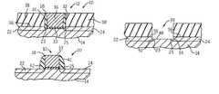
- a portion 10 of an integrated circuitincludes a transistor 12 disposed on a semiconductor substrate 14 , such as, a single crystal silicon wafer.
- substrate 14can be other semiconductor materials.
- Transistor 12is part of the integrated circuit (IC) manufactured on a wafer (such as, a single crystaline silicon wafer).
- Transistor 12includes a gate structure 18 , a source region 22 , and a drain region 24 . Transistor 12 also includes a source extension 23 and a drain extension 25 . Gate structure 18 is disposed between region 22 and region 24 .
- Extensions 23 and 25are preferably ultra-shallow extensions (e.g., junction depth or thickness less than 30 nanometers (nm)), which are thinner than regions 22 and 24 .
- extensions 23 and 25can have a thickness as large as 60 nm.
- Extensions 23 and 25are connected to regions 22 and 24 , respectively, and are disposed partially underneath a gate oxide 33 .
- Ultra-shallow extensions 23 and 25help transistor 12 achieve substantial immunity to short-channel effects. Short-channel effects can degrade performance of transistor 12 , as well as the manufacturability of the IC associated with transistor 12 .
- Gate oxide 33can be a 2-5 nm thick layer of thermally grown silicon dioxide. Alternatively, gate oxide 33 can be a silicon nitride (Si 3 N 4 ) material. Transistor 12 can be an N-channel or a P-channel field effect transistor, such as, a metal oxide semiconductor field effect transistor (MOSFET). Transistor 12 is preferably part of an ultra-large scale integrated (ULSI) circuit that includes one million or more transistors.
- ULSIultra-large scale integrated
- Gate structure 18includes a spacer 32 , gate oxide 33 , and a polysilicon gate conductor 36 .
- Spacer 32 and conductor 36are preferably deposited by chemical vapor deposition (CVD) and selectively etched to form the particular structures for transistor 12 .
- Spacer 32is preferably silicon dioxide or silicon nitride.
- Layer 38is provided over regions 22 and 24 .
- Layer 38can be provided by a low temperature (under 500° C.) CVD process over substrate 14 and structure 18 and subsequently polished by a chemical mechanical polish technique (CMP) to reduce the level of layer 38 to be approximately the same layer level as material 36 .
- Layer 38is preferably silicon dioxide deposited in a tetraorthosilicate (TEOS) process and is initially approximately 300 to 500 nm thick.
- TEOStetraorthosilicate
- Conductor 36preferably has a width of 100 to 250 nm and a thickness of 100 to 200 nm.
- Oxide 33is preferably thermally grown to a thickness of 2-5 nm. Oxide 33 is located below a top surface 56 of substrate 14 (above the bottom of the recess which forms extensions 23 and 25 out of regions 22 and 24 ).
- transistor 12can be substantially formed by conventional semiconductor processing techniques to form gate structure 18 , including a sacrificial gate oxide 35 , a dummy gate material 37 , source region 22 , and drain region 24 . Additionally, spacers 42 are provided partially over source region 22 and drain region 24 . Spacers 42 are sacrificial spacers. Spacers 42 are preferably formed by depositing silicon dioxide over gate structure 18 and selectively etching the silicon dioxide to leave spacers 42 . Spacers 42 preferably have a width of approximately 30-80 nm.
- substrate 14is doped in an ion implantation process to form source region 22 and drain region 24 .
- Regions 22 and 24extend deeply below a top surface 43 of substrate 14 (FIG. 2 ).
- a diffusion techniquecan be utilized to form regions 22 and 24 .
- Source region 22 and drain region 24can be heavily doped with boron or phosphorous, depending upon the type of transistor 12 .
- other dopantscan be utilized.
- Dummy gate 37is undoped polysilicon which is preferably protected when source region 22 and drain region 24 are doped.
- material 37can be any semiconductive material.
- Gate oxide 35is thermally grown silicon dioxide that is 10-20 nm thick.
- Substrate 14is subject to a rapid thermal annealing process to appropriately diffuse dopants within regions 22 and 24 substrate 14 .
- portion 10can be created with a self-aligned process.
- Gate structure 18 including dummy gate material 37 , sacrifical spacers 42 and sacrificial gate oxide 35serves to precisely position regions 22 and 24 with respect to structure 18 .
- layer 38is deposited over structure 18 and reduced by a CMP process to expose material 37 .
- material 37is removed, thereby leaving a cavity 39 in gate structure 18 .
- oxide 35is removed to expose top surface 43 of substrate 14 between source region 22 and drain region 24 of transistor 12 .
- Material 37can removed by a wet chemical etch to reach gate oxide 35 .
- Gate oxide 35is especially thick to protect substrate 14 from etching when material 37 is subjected to the wet chemical etch process.
- Oxide 35can be removed by a wet chemical etching process selective to oxide to reach top surface 43 of substrate 14 .
- etching of oxide 35removes spacers 42 associated with gate structure 18 .
- dry-etching techniquescan be utilized to remove material 37 and oxide 35 .
- substrate 14is etched to form a recessed portion 48 in cavity 39 .
- Recessed portion 48includes corners 52 and 54 , which engage source region 22 and drain region 24 , respectively.
- Substrate 14can be etched by any stripping or removal process, including plasma-etching, dry-etching, wet chemical etching, or reactive ion-etching. Substrate 14 is etched so cavity 39 is from 40-170 nm lower than top surface 56 .
- Recessed portion 48forms ultra-shallow source and drain extensions 23 and 25 .
- source and drain regions 22 and 24are approximately 100-200 nm below top surface 56 of substrate 14 and extensions 23 and 25 are between less than 30 and 60 nm thick. Accordingly, recessed portion 48 extends from approximately 40-170 nm below top surface 56 .
- spacers 32are preferably each 8-10 nm thick. Spacers 32 can be deposited by CVD and selectively etched after gate oxide 33 is formed. Gate oxide 33 is preferably a thin gate oxide having a thickness of approximately 2-5 nm.
- conductor 36is provided in cavity 39 .
- transistor 12can be manufactured without spacers 32 .
- Conductor 36is preferably provided as a conformal layer of doped polysilicon that is selectively etched to leave gate conductor 36 in structure 18 .
- conductor 36can be doped in a subsequent step.
- Conductor 36can be any doped semiconductor material or conductor.
- Conductor 36is preferably deposited as a 300-500 nm thick layer and is polished back to leave layer 38 .
- substrate 14is over-etched to form ultra-shallow source and drain extensions 22 and 24 , thereby circumventing problems associated with conventional ion implantation approaches.
- Conventional contacts, interconnects, and other CMOS processescan be utilized to complete the formation of the integrated circuit associated with portion 10 and transistor 12 .
Landscapes
- Insulated Gate Type Field-Effect Transistor (AREA)
Abstract
Description
Claims (20)
Priority Applications (2)
| Application Number | Priority Date | Filing Date | Title |
|---|---|---|---|
| US09/187,172US6225173B1 (en) | 1998-11-06 | 1998-11-06 | Recessed channel structure for manufacturing shallow source/drain extensions |
| US09/303,696US6297115B1 (en) | 1998-11-06 | 1999-05-03 | Cmos processs with low thermal budget |
Applications Claiming Priority (1)
| Application Number | Priority Date | Filing Date | Title |
|---|---|---|---|
| US09/187,172US6225173B1 (en) | 1998-11-06 | 1998-11-06 | Recessed channel structure for manufacturing shallow source/drain extensions |
Related Child Applications (1)
| Application Number | Title | Priority Date | Filing Date |
|---|---|---|---|
| US09/187,630Continuation-In-PartUS6180476B1 (en) | 1998-11-06 | 1998-11-06 | Dual amorphization implant process for ultra-shallow drain and source extensions |
Publications (1)
| Publication Number | Publication Date |
|---|---|
| US6225173B1true US6225173B1 (en) | 2001-05-01 |
Family
ID=22687883
Family Applications (1)
| Application Number | Title | Priority Date | Filing Date |
|---|---|---|---|
| US09/187,172Expired - LifetimeUS6225173B1 (en) | 1998-11-06 | 1998-11-06 | Recessed channel structure for manufacturing shallow source/drain extensions |
Country Status (1)
| Country | Link |
|---|---|
| US (1) | US6225173B1 (en) |
Cited By (41)
| Publication number | Priority date | Publication date | Assignee | Title |
|---|---|---|---|---|
| US20010046744A1 (en)* | 1999-01-13 | 2001-11-29 | Brian S. Doyle | Transistor with reduced series resistance junction regions |
| US6406963B2 (en)* | 1999-12-17 | 2002-06-18 | Koninklijke Philips Electronics N.A. | Method of manufacturing a semiconductor device |
| US6432781B2 (en)* | 2000-06-19 | 2002-08-13 | Texas Instruments Incorporated | Inverted MOSFET process |
| US6521502B1 (en) | 2000-08-07 | 2003-02-18 | Advanced Micro Devices, Inc. | Solid phase epitaxy activation process for source/drain junction extensions and halo regions |
| US6534372B1 (en)* | 2000-11-22 | 2003-03-18 | Newport Fab, Llc | Method for fabricating a self-aligned emitter in a bipolar transistor |
| US6566215B1 (en)* | 2002-06-06 | 2003-05-20 | Chartered Semiconductor Manufacturing Ltd. | Method of fabricating short channel MOS transistors with source/drain extensions |
| US6613621B2 (en)* | 2000-03-09 | 2003-09-02 | Samsung Electronics Co., Ltd. | Methods of forming self-aligned contact pads using a damascene gate process |
| US6630386B1 (en) | 2000-07-18 | 2003-10-07 | Advanced Micro Devices, Inc | CMOS manufacturing process with self-amorphized source/drain junctions and extensions |
| US6649460B2 (en) | 2001-10-25 | 2003-11-18 | International Business Machines Corporation | Fabricating a substantially self-aligned MOSFET |
| US6660598B2 (en) | 2002-02-26 | 2003-12-09 | International Business Machines Corporation | Method of forming a fully-depleted SOI ( silicon-on-insulator) MOSFET having a thinned channel region |
| US6677646B2 (en) | 2002-04-05 | 2004-01-13 | International Business Machines Corporation | Method and structure of a disposable reversed spacer process for high performance recessed channel CMOS |
| US20040056307A1 (en)* | 2002-09-19 | 2004-03-25 | Won-Ju Cho | Ultra small-sized soi mosfet and method of fabricating the same |
| US6727151B2 (en) | 2002-08-07 | 2004-04-27 | Chartered Semiconductor Manufacturing Ltd. | Method to fabricate elevated source/drain structures in MOS transistors |
| EP1435647A1 (en)* | 2002-12-30 | 2004-07-07 | STMicroelectronics S.r.l. | Method for forming structures self-aligned with each other on a semiconductor substrate |
| US6764884B1 (en)* | 2003-04-03 | 2004-07-20 | Advanced Micro Devices, Inc. | Method for forming a gate in a FinFET device and thinning a fin in a channel region of the FinFET device |
| US20040159884A1 (en)* | 2000-03-31 | 2004-08-19 | Fumitomo Matsuoka | Semiconductor device and a method for manufacturing the same |
| US20040203198A1 (en)* | 2003-04-01 | 2004-10-14 | Wonju Cho | MOSFET device with nanoscale channel and method of manufacturing the same |
| US20050009250A1 (en)* | 2003-06-27 | 2005-01-13 | Wonju Cho | Ultra short channel field effect transistor and method of fabricating the same |
| US6870225B2 (en)* | 2001-11-02 | 2005-03-22 | International Business Machines Corporation | Transistor structure with thick recessed source/drain structures and fabrication process of same |
| US20050090066A1 (en)* | 2003-10-22 | 2005-04-28 | International Business Machines Corporation | Method and manufacture of thin silicon on insulator (soi) with recessed channel and devices manufactured thereby |
| US20050133830A1 (en)* | 2003-12-17 | 2005-06-23 | Taiwan Semiconductor Manufacturing Co., Ltd. | Method for fabricating a recessed channel filed effect transistor (FET) device |
| US20050153485A1 (en)* | 2004-01-12 | 2005-07-14 | Ahmed Shibly S. | Narrow-body damascene tri-gate FinFET |
| US6967175B1 (en) | 2003-12-04 | 2005-11-22 | Advanced Micro Devices, Inc. | Damascene gate semiconductor processing with local thinning of channel region |
| US20060019447A1 (en)* | 2004-07-20 | 2006-01-26 | Martin Gutsche | Process for the self-aligning production of a transistor with a U-shaped gate |
| US20060038241A1 (en)* | 2002-09-12 | 2006-02-23 | Kabushiki Kaisha Toshiba | Semiconductor device and method of manufacturing the same |
| US20060091432A1 (en)* | 2004-11-02 | 2006-05-04 | International Business Machines Corporation | Damascene gate field effect transistor with an internal spacer structure |
| US7067377B1 (en) | 2004-03-30 | 2006-06-27 | Fasl Llc | Recessed channel with separated ONO memory device |
| US20060141720A1 (en)* | 2004-12-29 | 2006-06-29 | Lee Yong G | Method of fabricating MOS transistor |
| US20080254606A1 (en)* | 2005-12-06 | 2008-10-16 | In Bok Baek | Method of Manufacturing Semiconductor Device |
| US20080305621A1 (en)* | 2007-06-08 | 2008-12-11 | International Business Machines Corporation | Channel strain engineering in field-effect-transistor |
| US20090108293A1 (en)* | 2007-10-30 | 2009-04-30 | Victor Moroz | Method for Suppressing Lattice Defects in a Semiconductor Substrate |
| US20090302412A1 (en)* | 2008-06-04 | 2009-12-10 | International Business Machines Corporation | Carrier mobility enhanced channel devices and method of manufacture |
| US7804130B1 (en) | 2008-08-26 | 2010-09-28 | Taiwan Semiconductor Manufacturing Co., Ltd. | Self-aligned V-channel MOSFET |
| US20110078639A1 (en)* | 2007-10-26 | 2011-03-31 | Synopsys, Inc. | Filler cells for design optimization in a place-and-route system |
| US20110291184A1 (en)* | 2010-05-26 | 2011-12-01 | Institute of Microelectronics, Chinese Academy of Sciences | Semiconductor structure and method for manufacturing the same |
| US8368147B2 (en) | 2010-04-16 | 2013-02-05 | Taiwan Semiconductor Manufacturing Company, Ltd. | Strained semiconductor device with recessed channel |
| US8445345B2 (en)* | 2011-09-08 | 2013-05-21 | International Business Machines Corporation | CMOS structure having multiple threshold voltage devices |
| CN103383914A (en)* | 2012-05-02 | 2013-11-06 | 中国科学院微电子研究所 | Semiconductor structure and manufacturing method thereof |
| US20150295070A1 (en)* | 2012-11-16 | 2015-10-15 | Institute of Microelectronics, Chinese Academy of Sciences | Finfet and method for manufacturing the same |
| US9698054B2 (en) | 2010-10-19 | 2017-07-04 | Taiwan Semiconductor Manufacturing Company, Ltd. | Strained structure of a p-type field effect transistor |
| US11195935B2 (en)* | 2018-04-19 | 2021-12-07 | Globalfoundries U.S. Inc. | Semiconductor device with novel spacer structures having novel configurations |
Citations (37)
| Publication number | Priority date | Publication date | Assignee | Title |
|---|---|---|---|---|
| US4683645A (en) | 1985-06-28 | 1987-08-04 | Northern Telecom Limited | Process of fabricating MOS devices having shallow source and drain junctions |
| US4745082A (en) | 1986-06-12 | 1988-05-17 | Ford Microelectronics, Inc. | Method of making a self-aligned MESFET using a substitutional gate with side walls |
| US4784718A (en) | 1986-02-27 | 1988-11-15 | Kabushiki Kaisha Toshiba | Method for manufacturing semiconductor device |
| US5017504A (en)* | 1986-12-01 | 1991-05-21 | Mitsubishi Denki Kabushiki Kaisha | Vertical type MOS transistor and method of formation thereof |
| JPH03248433A (en) | 1990-02-26 | 1991-11-06 | Nec Corp | Manufacturing method of semiconductor device |
| JPH04123439A (en) | 1990-09-14 | 1992-04-23 | Toshiba Corp | Manufacture of semiconductor device |
| JPH05160396A (en) | 1991-12-06 | 1993-06-25 | Sharp Corp | MOS field effect transistor |
| US5264382A (en) | 1990-03-20 | 1993-11-23 | Fujitsu Limited | Method of producing semiconductor device using dummy gate structure |
| US5270232A (en)* | 1991-09-13 | 1993-12-14 | Hitachi, Ltd. | Process for fabricating field effect transistor |
| US5374575A (en) | 1993-11-23 | 1994-12-20 | Goldstar Electron Co., Ltd. | Method for fabricating MOS transistor |
| US5391510A (en) | 1992-02-28 | 1995-02-21 | International Business Machines Corporation | Formation of self-aligned metal gate FETs using a benignant removable gate material during high temperature steps |
| US5393685A (en) | 1992-08-10 | 1995-02-28 | Taiwan Semiconductor Manufacturing Company | Peeling free metal silicide films using rapid thermal anneal |
| US5429956A (en) | 1994-09-30 | 1995-07-04 | United Microelectronics Corporation | Method for fabricating a field effect transistor with a self-aligned anti-punchthrough implant channel |
| US5434093A (en)* | 1994-08-10 | 1995-07-18 | Intel Corporation | Inverted spacer transistor |
| US5538913A (en)* | 1995-11-13 | 1996-07-23 | United Microelectronics Corporation | Process for fabricating MOS transistors having full-overlap lightly-doped drain structure |
| US5576227A (en)* | 1994-11-02 | 1996-11-19 | United Microelectronics Corp. | Process for fabricating a recessed gate MOS device |
| US5593907A (en) | 1995-03-08 | 1997-01-14 | Advanced Micro Devices | Large tilt angle boron implant methodology for reducing subthreshold current in NMOS integrated circuit devices |
| US5607884A (en) | 1993-12-16 | 1997-03-04 | Lg Semicon Co., Ltd. | Method for fabricating MOS transistor having source/drain region of shallow junction and silicide film |
| US5675159A (en) | 1995-03-24 | 1997-10-07 | Mitsubishi Denki Kabushiki Kaisha | Recessed gate field effect transistor |
| US5716861A (en) | 1991-06-26 | 1998-02-10 | Texas Instruments Incorporated | Insulated-gate field-effect transistor structure and method |
| US5736435A (en)* | 1995-07-03 | 1998-04-07 | Motorola, Inc. | Process for fabricating a fully self-aligned soi mosfet |
| US5793090A (en) | 1997-01-10 | 1998-08-11 | Advanced Micro Devices, Inc. | Integrated circuit having multiple LDD and/or source/drain implant steps to enhance circuit performance |
| US5801075A (en)* | 1996-10-30 | 1998-09-01 | Advanced Micro Devices, Inc. | Method of forming trench transistor with metal spacers |
| US5811323A (en) | 1990-11-16 | 1998-09-22 | Seiko Epson Corporation | Process for fabricating a thin film transistor |
| US5814544A (en)* | 1994-07-14 | 1998-09-29 | Vlsi Technology, Inc. | Forming a MOS transistor with a recessed channel |
| US5817558A (en)* | 1997-06-20 | 1998-10-06 | Acer Semiconductor Manufacturing Inc. | Method of forming a T-gate Lightly-Doped Drain semiconductor device |
| US5825066A (en) | 1996-05-08 | 1998-10-20 | Advanced Micro Devices, Inc. | Control of juction depth and channel length using generated interstitial gradients to oppose dopant diffusion |
| US5824586A (en)* | 1996-10-23 | 1998-10-20 | Advanced Micro Devices, Inc. | Method of manufacturing a raised source/drain MOSFET |
| US5856225A (en)* | 1997-11-24 | 1999-01-05 | Chartered Semiconductor Manufacturing Ltd | Creation of a self-aligned, ion implanted channel region, after source and drain formation |
| US5858843A (en) | 1996-09-27 | 1999-01-12 | Intel Corporation | Low temperature method of forming gate electrode and gate dielectric |
| US5904530A (en)* | 1991-05-15 | 1999-05-18 | Goldstar Electron Co., Ltd. | Method of making LDD structure spaced from channel doped region |
| US5915180A (en)* | 1994-04-06 | 1999-06-22 | Denso Corporation | Process for producing a semiconductor device having a single thermal oxidizing step |
| US5915183A (en)* | 1998-06-26 | 1999-06-22 | International Business Machines Corporation | Raised source/drain using recess etch of polysilicon |
| US5937297A (en)* | 1998-06-01 | 1999-08-10 | Chartered Semiconductor Manufacturing, Ltd. | Method for making sub-quarter-micron MOSFET |
| US5953602A (en)* | 1995-05-26 | 1999-09-14 | Lg Semicon Co., Ltd. | EEPROM cell and related method of making thereof |
| US5972754A (en)* | 1998-06-10 | 1999-10-26 | Mosel Vitelic, Inc. | Method for fabricating MOSFET having increased effective gate length |
| US5998288A (en)* | 1998-04-17 | 1999-12-07 | Advanced Micro Devices, Inc. | Ultra thin spacers formed laterally adjacent a gate conductor recessed below the upper surface of a substrate |
- 1998
- 1998-11-06USUS09/187,172patent/US6225173B1/ennot_activeExpired - Lifetime
Patent Citations (37)
| Publication number | Priority date | Publication date | Assignee | Title |
|---|---|---|---|---|
| US4683645A (en) | 1985-06-28 | 1987-08-04 | Northern Telecom Limited | Process of fabricating MOS devices having shallow source and drain junctions |
| US4784718A (en) | 1986-02-27 | 1988-11-15 | Kabushiki Kaisha Toshiba | Method for manufacturing semiconductor device |
| US4745082A (en) | 1986-06-12 | 1988-05-17 | Ford Microelectronics, Inc. | Method of making a self-aligned MESFET using a substitutional gate with side walls |
| US5017504A (en)* | 1986-12-01 | 1991-05-21 | Mitsubishi Denki Kabushiki Kaisha | Vertical type MOS transistor and method of formation thereof |
| JPH03248433A (en) | 1990-02-26 | 1991-11-06 | Nec Corp | Manufacturing method of semiconductor device |
| US5264382A (en) | 1990-03-20 | 1993-11-23 | Fujitsu Limited | Method of producing semiconductor device using dummy gate structure |
| JPH04123439A (en) | 1990-09-14 | 1992-04-23 | Toshiba Corp | Manufacture of semiconductor device |
| US5811323A (en) | 1990-11-16 | 1998-09-22 | Seiko Epson Corporation | Process for fabricating a thin film transistor |
| US5904530A (en)* | 1991-05-15 | 1999-05-18 | Goldstar Electron Co., Ltd. | Method of making LDD structure spaced from channel doped region |
| US5716861A (en) | 1991-06-26 | 1998-02-10 | Texas Instruments Incorporated | Insulated-gate field-effect transistor structure and method |
| US5270232A (en)* | 1991-09-13 | 1993-12-14 | Hitachi, Ltd. | Process for fabricating field effect transistor |
| JPH05160396A (en) | 1991-12-06 | 1993-06-25 | Sharp Corp | MOS field effect transistor |
| US5391510A (en) | 1992-02-28 | 1995-02-21 | International Business Machines Corporation | Formation of self-aligned metal gate FETs using a benignant removable gate material during high temperature steps |
| US5393685A (en) | 1992-08-10 | 1995-02-28 | Taiwan Semiconductor Manufacturing Company | Peeling free metal silicide films using rapid thermal anneal |
| US5374575A (en) | 1993-11-23 | 1994-12-20 | Goldstar Electron Co., Ltd. | Method for fabricating MOS transistor |
| US5607884A (en) | 1993-12-16 | 1997-03-04 | Lg Semicon Co., Ltd. | Method for fabricating MOS transistor having source/drain region of shallow junction and silicide film |
| US5915180A (en)* | 1994-04-06 | 1999-06-22 | Denso Corporation | Process for producing a semiconductor device having a single thermal oxidizing step |
| US5814544A (en)* | 1994-07-14 | 1998-09-29 | Vlsi Technology, Inc. | Forming a MOS transistor with a recessed channel |
| US5434093A (en)* | 1994-08-10 | 1995-07-18 | Intel Corporation | Inverted spacer transistor |
| US5429956A (en) | 1994-09-30 | 1995-07-04 | United Microelectronics Corporation | Method for fabricating a field effect transistor with a self-aligned anti-punchthrough implant channel |
| US5576227A (en)* | 1994-11-02 | 1996-11-19 | United Microelectronics Corp. | Process for fabricating a recessed gate MOS device |
| US5593907A (en) | 1995-03-08 | 1997-01-14 | Advanced Micro Devices | Large tilt angle boron implant methodology for reducing subthreshold current in NMOS integrated circuit devices |
| US5675159A (en) | 1995-03-24 | 1997-10-07 | Mitsubishi Denki Kabushiki Kaisha | Recessed gate field effect transistor |
| US5953602A (en)* | 1995-05-26 | 1999-09-14 | Lg Semicon Co., Ltd. | EEPROM cell and related method of making thereof |
| US5736435A (en)* | 1995-07-03 | 1998-04-07 | Motorola, Inc. | Process for fabricating a fully self-aligned soi mosfet |
| US5538913A (en)* | 1995-11-13 | 1996-07-23 | United Microelectronics Corporation | Process for fabricating MOS transistors having full-overlap lightly-doped drain structure |
| US5825066A (en) | 1996-05-08 | 1998-10-20 | Advanced Micro Devices, Inc. | Control of juction depth and channel length using generated interstitial gradients to oppose dopant diffusion |
| US5858843A (en) | 1996-09-27 | 1999-01-12 | Intel Corporation | Low temperature method of forming gate electrode and gate dielectric |
| US5824586A (en)* | 1996-10-23 | 1998-10-20 | Advanced Micro Devices, Inc. | Method of manufacturing a raised source/drain MOSFET |
| US5801075A (en)* | 1996-10-30 | 1998-09-01 | Advanced Micro Devices, Inc. | Method of forming trench transistor with metal spacers |
| US5793090A (en) | 1997-01-10 | 1998-08-11 | Advanced Micro Devices, Inc. | Integrated circuit having multiple LDD and/or source/drain implant steps to enhance circuit performance |
| US5817558A (en)* | 1997-06-20 | 1998-10-06 | Acer Semiconductor Manufacturing Inc. | Method of forming a T-gate Lightly-Doped Drain semiconductor device |
| US5856225A (en)* | 1997-11-24 | 1999-01-05 | Chartered Semiconductor Manufacturing Ltd | Creation of a self-aligned, ion implanted channel region, after source and drain formation |
| US5998288A (en)* | 1998-04-17 | 1999-12-07 | Advanced Micro Devices, Inc. | Ultra thin spacers formed laterally adjacent a gate conductor recessed below the upper surface of a substrate |
| US5937297A (en)* | 1998-06-01 | 1999-08-10 | Chartered Semiconductor Manufacturing, Ltd. | Method for making sub-quarter-micron MOSFET |
| US5972754A (en)* | 1998-06-10 | 1999-10-26 | Mosel Vitelic, Inc. | Method for fabricating MOSFET having increased effective gate length |
| US5915183A (en)* | 1998-06-26 | 1999-06-22 | International Business Machines Corporation | Raised source/drain using recess etch of polysilicon |
Non-Patent Citations (3)
| Title |
|---|
| "Sub 50-nm Fin FET: PMOS" Huang, et al. 1999 IEEE. |
| "Ultra-Thin-Body Silicon-On-Insulator MOSFET's for Terabit-Scale Integration" Yu, et al., 12/97. |
| IEDM Technical Digest International Electronic Device Meeting 1997 "Sub-100nm Gate Length Metal Gate NMOS Transistors Fabricated by a Replacement Gate Process" by Chatterjee, et al. 1997 IEEE. |
Cited By (84)
| Publication number | Priority date | Publication date | Assignee | Title |
|---|---|---|---|---|
| US20010046744A1 (en)* | 1999-01-13 | 2001-11-29 | Brian S. Doyle | Transistor with reduced series resistance junction regions |
| US6406963B2 (en)* | 1999-12-17 | 2002-06-18 | Koninklijke Philips Electronics N.A. | Method of manufacturing a semiconductor device |
| US6743682B2 (en)* | 1999-12-17 | 2004-06-01 | Koninklijke Philips Electronics N.V. | Method of manufacturing a semiconductor device |
| US6613621B2 (en)* | 2000-03-09 | 2003-09-02 | Samsung Electronics Co., Ltd. | Methods of forming self-aligned contact pads using a damascene gate process |
| US20040159884A1 (en)* | 2000-03-31 | 2004-08-19 | Fumitomo Matsuoka | Semiconductor device and a method for manufacturing the same |
| US6432781B2 (en)* | 2000-06-19 | 2002-08-13 | Texas Instruments Incorporated | Inverted MOSFET process |
| US6630386B1 (en) | 2000-07-18 | 2003-10-07 | Advanced Micro Devices, Inc | CMOS manufacturing process with self-amorphized source/drain junctions and extensions |
| US6521502B1 (en) | 2000-08-07 | 2003-02-18 | Advanced Micro Devices, Inc. | Solid phase epitaxy activation process for source/drain junction extensions and halo regions |
| US6716711B1 (en) | 2000-11-22 | 2004-04-06 | Newport Fab, Llc | Method for fabricating a self-aligned emitter in a bipolar transistor |
| US6534372B1 (en)* | 2000-11-22 | 2003-03-18 | Newport Fab, Llc | Method for fabricating a self-aligned emitter in a bipolar transistor |
| US6649460B2 (en) | 2001-10-25 | 2003-11-18 | International Business Machines Corporation | Fabricating a substantially self-aligned MOSFET |
| US6870225B2 (en)* | 2001-11-02 | 2005-03-22 | International Business Machines Corporation | Transistor structure with thick recessed source/drain structures and fabrication process of same |
| US20050101072A1 (en)* | 2001-11-02 | 2005-05-12 | Andres Bryant | Transistor structure with thick recessed source/drain structures and fabrication process of same |
| US7132339B2 (en) | 2001-11-02 | 2006-11-07 | International Business Machines Corporation | Transistor structure with thick recessed source/drain structures and fabrication process of same |
| US6660598B2 (en) | 2002-02-26 | 2003-12-09 | International Business Machines Corporation | Method of forming a fully-depleted SOI ( silicon-on-insulator) MOSFET having a thinned channel region |
| US6841831B2 (en) | 2002-02-26 | 2005-01-11 | International Business Machines Corporation | Fully-depleted SOI MOSFETs with low source and drain resistance and minimal overlap capacitance using a recessed channel damascene gate process |
| US6677646B2 (en) | 2002-04-05 | 2004-01-13 | International Business Machines Corporation | Method and structure of a disposable reversed spacer process for high performance recessed channel CMOS |
| US20040104433A1 (en)* | 2002-04-05 | 2004-06-03 | International Business Machines Corporation | Method and structure of a disposable reversed spacer process for high performance recessed channel CMOS |
| US7041538B2 (en) | 2002-04-05 | 2006-05-09 | International Business Machines Corporation | Method of manufacturing a disposable reversed spacer process for high performance recessed channel CMOS |
| US6566215B1 (en)* | 2002-06-06 | 2003-05-20 | Chartered Semiconductor Manufacturing Ltd. | Method of fabricating short channel MOS transistors with source/drain extensions |
| US6727151B2 (en) | 2002-08-07 | 2004-04-27 | Chartered Semiconductor Manufacturing Ltd. | Method to fabricate elevated source/drain structures in MOS transistors |
| US7767535B2 (en)* | 2002-09-12 | 2010-08-03 | Kabushiki Kaisha Toshiba | Semiconductor device and method of manufacturing the same |
| US20060038241A1 (en)* | 2002-09-12 | 2006-02-23 | Kabushiki Kaisha Toshiba | Semiconductor device and method of manufacturing the same |
| US6723587B2 (en) | 2002-09-19 | 2004-04-20 | Electronics And Telecommunications Research Institute | Ultra small-sized SOI MOSFET and method of fabricating the same |
| US20040056307A1 (en)* | 2002-09-19 | 2004-03-25 | Won-Ju Cho | Ultra small-sized soi mosfet and method of fabricating the same |
| US20040188757A1 (en)* | 2002-12-30 | 2004-09-30 | Livio Baldi | Method for forming structures self-aligned with each other on a semiconductor substrate |
| EP1435647A1 (en)* | 2002-12-30 | 2004-07-07 | STMicroelectronics S.r.l. | Method for forming structures self-aligned with each other on a semiconductor substrate |
| US20040203198A1 (en)* | 2003-04-01 | 2004-10-14 | Wonju Cho | MOSFET device with nanoscale channel and method of manufacturing the same |
| US6995452B2 (en) | 2003-04-01 | 2006-02-07 | Electronics And Telecommunications Research Institute | MOSFET device with nanoscale channel and method of manufacturing the same |
| KR101079348B1 (en)* | 2003-04-03 | 2011-11-04 | 어드밴스드 마이크로 디바이시즈, 인코포레이티드 | Method for forming a gate in a finfet device and thinning a fin in a channel region of the finfet device |
| US6764884B1 (en)* | 2003-04-03 | 2004-07-20 | Advanced Micro Devices, Inc. | Method for forming a gate in a FinFET device and thinning a fin in a channel region of the FinFET device |
| US7195962B2 (en) | 2003-06-27 | 2007-03-27 | Electronics And Telecommunications Research Institute | Ultra short channel field effect transistor and method of fabricating the same |
| US20050009250A1 (en)* | 2003-06-27 | 2005-01-13 | Wonju Cho | Ultra short channel field effect transistor and method of fabricating the same |
| US20050090066A1 (en)* | 2003-10-22 | 2005-04-28 | International Business Machines Corporation | Method and manufacture of thin silicon on insulator (soi) with recessed channel and devices manufactured thereby |
| US6939751B2 (en) | 2003-10-22 | 2005-09-06 | International Business Machines Corporation | Method and manufacture of thin silicon on insulator (SOI) with recessed channel |
| US6967175B1 (en) | 2003-12-04 | 2005-11-22 | Advanced Micro Devices, Inc. | Damascene gate semiconductor processing with local thinning of channel region |
| US6974730B2 (en) | 2003-12-17 | 2005-12-13 | Taiwan Semiconductor Manufacturing Co., Ltd. | Method for fabricating a recessed channel field effect transistor (FET) device |
| US20060033158A1 (en)* | 2003-12-17 | 2006-02-16 | Diaz Carlos H | Method for fabricating a recessed channel field effect transistor (FET) device |
| US7429769B2 (en) | 2003-12-17 | 2008-09-30 | Taiwan Semiconductor Manufacturing Co., Ltd | Recessed channel field effect transistor (FET) device |
| US20050133830A1 (en)* | 2003-12-17 | 2005-06-23 | Taiwan Semiconductor Manufacturing Co., Ltd. | Method for fabricating a recessed channel filed effect transistor (FET) device |
| US20050153485A1 (en)* | 2004-01-12 | 2005-07-14 | Ahmed Shibly S. | Narrow-body damascene tri-gate FinFET |
| US7186599B2 (en) | 2004-01-12 | 2007-03-06 | Advanced Micro Devices, Inc. | Narrow-body damascene tri-gate FinFET |
| US7394125B1 (en) | 2004-03-30 | 2008-07-01 | Fasl Llc | Recessed channel with separated ONO memory device |
| US7067377B1 (en) | 2004-03-30 | 2006-06-27 | Fasl Llc | Recessed channel with separated ONO memory device |
| DE102004035108B4 (en)* | 2004-07-20 | 2010-07-15 | Qimonda Ag | Method for the self-aligning production of a U-shaped transistor and selection transistor for a memory cell |
| DE102004035108A1 (en)* | 2004-07-20 | 2006-02-09 | Infineon Technologies Ag | Method for self-aligning a U-shaped transistor |
| US20060019447A1 (en)* | 2004-07-20 | 2006-01-26 | Martin Gutsche | Process for the self-aligning production of a transistor with a U-shaped gate |
| US7479684B2 (en)* | 2004-11-02 | 2009-01-20 | International Business Machines Corporation | Field effect transistor including damascene gate with an internal spacer structure |
| US20090124057A1 (en)* | 2004-11-02 | 2009-05-14 | International Business Machines Corporation | Damascene gate field effect transistor with an internal spacer structure |
| US20060091432A1 (en)* | 2004-11-02 | 2006-05-04 | International Business Machines Corporation | Damascene gate field effect transistor with an internal spacer structure |
| US7723196B2 (en)* | 2004-11-02 | 2010-05-25 | International Business Machines Corporation | Damascene gate field effect transistor with an internal spacer structure |
| US7625800B2 (en)* | 2004-12-29 | 2009-12-01 | Dongbu Electronics Co., Ltd. | Method of fabricating MOS transistor |
| US20060141720A1 (en)* | 2004-12-29 | 2006-06-29 | Lee Yong G | Method of fabricating MOS transistor |
| US20080254606A1 (en)* | 2005-12-06 | 2008-10-16 | In Bok Baek | Method of Manufacturing Semiconductor Device |
| US7947585B2 (en) | 2005-12-06 | 2011-05-24 | Electronics And Telecommunications Research Institute | Method of manufacturing semiconductor device |
| WO2008150557A1 (en)* | 2007-06-08 | 2008-12-11 | International Business Machines Corporation | Channel strain engineering in field-effect-transistor |
| US20080305621A1 (en)* | 2007-06-08 | 2008-12-11 | International Business Machines Corporation | Channel strain engineering in field-effect-transistor |
| US7842592B2 (en) | 2007-06-08 | 2010-11-30 | International Business Machines Corporation | Channel strain engineering in field-effect-transistor |
| CN101796641B (en)* | 2007-06-08 | 2012-02-29 | 国际商业机器公司 | Channel Strain Design in Field Effect Transistors |
| US8504969B2 (en) | 2007-10-26 | 2013-08-06 | Synopsys, Inc. | Filler cells for design optimization in a place-and-route system |
| US20110078639A1 (en)* | 2007-10-26 | 2011-03-31 | Synopsys, Inc. | Filler cells for design optimization in a place-and-route system |
| US9472423B2 (en) | 2007-10-30 | 2016-10-18 | Synopsys, Inc. | Method for suppressing lattice defects in a semiconductor substrate |
| US20100025777A1 (en)* | 2007-10-30 | 2010-02-04 | Synopsys, Inc. | Method for suppressing lattice defects in a semiconductor substrate |
| US20090108293A1 (en)* | 2007-10-30 | 2009-04-30 | Victor Moroz | Method for Suppressing Lattice Defects in a Semiconductor Substrate |
| WO2009148992A1 (en)* | 2008-06-04 | 2009-12-10 | International Business Machines Corporation | Carrier mobility enhanced channel devices and method of manufacture |
| US20110180853A1 (en)* | 2008-06-04 | 2011-07-28 | International Business Machines Corporation | Carrier mobility enhanced channel devices and method of manufacture |
| US7964487B2 (en) | 2008-06-04 | 2011-06-21 | International Business Machines Corporation | Carrier mobility enhanced channel devices and method of manufacture |
| US20090302412A1 (en)* | 2008-06-04 | 2009-12-10 | International Business Machines Corporation | Carrier mobility enhanced channel devices and method of manufacture |
| US8461625B2 (en) | 2008-06-04 | 2013-06-11 | International Business Machines Corporation | Carrier mobility enhanced channel devices and method of manufacture |
| US8153492B2 (en) | 2008-08-26 | 2012-04-10 | Taiwan Semiconductor Manufacturing Company, Ltd. | Self-aligned V-channel MOSFET |
| US20110008940A1 (en)* | 2008-08-26 | 2011-01-13 | Taiwan Semiconductor Manufacturing Co., Ltd. | Self-aligned v-channel mosfet |
| US7804130B1 (en) | 2008-08-26 | 2010-09-28 | Taiwan Semiconductor Manufacturing Co., Ltd. | Self-aligned V-channel MOSFET |
| US8368147B2 (en) | 2010-04-16 | 2013-02-05 | Taiwan Semiconductor Manufacturing Company, Ltd. | Strained semiconductor device with recessed channel |
| US20110291184A1 (en)* | 2010-05-26 | 2011-12-01 | Institute of Microelectronics, Chinese Academy of Sciences | Semiconductor structure and method for manufacturing the same |
| US8399315B2 (en)* | 2010-05-26 | 2013-03-19 | Institute of Microelectronics, Chinese Academy of Sciences | Semiconductor structure and method for manufacturing the same |
| US9698054B2 (en) | 2010-10-19 | 2017-07-04 | Taiwan Semiconductor Manufacturing Company, Ltd. | Strained structure of a p-type field effect transistor |
| US10727340B2 (en) | 2010-10-19 | 2020-07-28 | Taiwan Semiconductor Manufacturing Company, Ltd. | Strained structure of a semiconductor device |
| US11329159B2 (en) | 2010-10-19 | 2022-05-10 | Taiwan Semiconductor Manufacturing Company, Ltd. | Strained structure of a semiconductor device |
| US8445345B2 (en)* | 2011-09-08 | 2013-05-21 | International Business Machines Corporation | CMOS structure having multiple threshold voltage devices |
| US8530974B2 (en) | 2011-09-08 | 2013-09-10 | International Business Machines Corporation | CMOS structure having multiple threshold voltage devices |
| CN103383914A (en)* | 2012-05-02 | 2013-11-06 | 中国科学院微电子研究所 | Semiconductor structure and manufacturing method thereof |
| US20140191311A1 (en)* | 2012-05-02 | 2014-07-10 | Institute of Microelectronics, Chinese Academy of Sciences | Semiconductor structure and method for manufacturing the same |
| US20150295070A1 (en)* | 2012-11-16 | 2015-10-15 | Institute of Microelectronics, Chinese Academy of Sciences | Finfet and method for manufacturing the same |
| US11195935B2 (en)* | 2018-04-19 | 2021-12-07 | Globalfoundries U.S. Inc. | Semiconductor device with novel spacer structures having novel configurations |
Similar Documents
| Publication | Publication Date | Title |
|---|---|---|
| US6225173B1 (en) | Recessed channel structure for manufacturing shallow source/drain extensions | |
| US5985726A (en) | Damascene process for forming ultra-shallow source/drain extensions and pocket in ULSI MOSFET | |
| KR100844933B1 (en) | Transistor of semiconductor device and manufacturing method thereof | |
| EP1192655B1 (en) | Method for eliminating stress induced dislocation in cmos devices | |
| US6248637B1 (en) | Process for manufacturing MOS Transistors having elevated source and drain regions | |
| US6300201B1 (en) | Method to form a high K dielectric gate insulator layer, a metal gate structure, and self-aligned channel regions, post source/drain formation | |
| US6184097B1 (en) | Process for forming ultra-shallow source/drain extensions | |
| US6828630B2 (en) | CMOS device on ultrathin SOI with a deposited raised source/drain, and a method of manufacture | |
| US5959333A (en) | Reduction of dopant diffusion by the co-implantation of impurities into the transistor gate conductor | |
| US6297132B1 (en) | Process to control the lateral doping profile of an implanted channel region | |
| KR100344733B1 (en) | Recessed-gate mosfet with out-diffused source/drain extension | |
| US6630712B2 (en) | Transistor with dynamic source/drain extensions | |
| US6372589B1 (en) | Method of forming ultra-shallow source/drain extension by impurity diffusion from doped dielectric spacer | |
| US7994010B2 (en) | Process for fabricating a semiconductor device having embedded epitaxial regions | |
| US20120034746A1 (en) | Methods of Fabricating MOS Transistors Having Recesses With Elevated Source/Drain Regions | |
| US20020060346A1 (en) | Method for making transistor structure having silicide source/drain extensions | |
| JP3821707B2 (en) | Manufacturing method of semiconductor device | |
| US20050095820A1 (en) | Technique for forming transistors having raised drain and source regions with different heights | |
| US5834350A (en) | Elevated transistor fabrication technique | |
| US6391728B1 (en) | Method of forming a highly localized halo profile to prevent punch-through | |
| US20020090787A1 (en) | Self-aligned elevated transistor | |
| US6074904A (en) | Method and structure for isolating semiconductor devices after transistor formation | |
| US6737315B2 (en) | Method of manufacturing semiconductor device including steps of forming both insulating film and epitaxial semiconductor on substrate | |
| US20080070356A1 (en) | Trench replacement gate process for transistors having elevated source and drain regions | |
| US7217625B2 (en) | Method of fabricating a semiconductor device having a shallow source/drain region |
Legal Events
| Date | Code | Title | Description |
|---|---|---|---|
| AS | Assignment | Owner name:ADVANCED MICRO DEVICES, INC., CALIFORNIA Free format text:ASSIGNMENT OF ASSIGNORS INTEREST;ASSIGNOR:YU, BIN;REEL/FRAME:009571/0749 Effective date:19981019 | |
| STCF | Information on status: patent grant | Free format text:PATENTED CASE | |
| FEPP | Fee payment procedure | Free format text:PAYOR NUMBER ASSIGNED (ORIGINAL EVENT CODE: ASPN); ENTITY STATUS OF PATENT OWNER: LARGE ENTITY | |
| FPAY | Fee payment | Year of fee payment:4 | |
| FEPP | Fee payment procedure | Free format text:PAYER NUMBER DE-ASSIGNED (ORIGINAL EVENT CODE: RMPN); ENTITY STATUS OF PATENT OWNER: LARGE ENTITY Free format text:PAYOR NUMBER ASSIGNED (ORIGINAL EVENT CODE: ASPN); ENTITY STATUS OF PATENT OWNER: LARGE ENTITY | |
| FPAY | Fee payment | Year of fee payment:8 | |
| AS | Assignment | Owner name:GLOBALFOUNDRIES INC., CAYMAN ISLANDS Free format text:AFFIRMATION OF PATENT ASSIGNMENT;ASSIGNOR:ADVANCED MICRO DEVICES, INC.;REEL/FRAME:023119/0083 Effective date:20090630 | |
| FPAY | Fee payment | Year of fee payment:12 | |
| AS | Assignment | Owner name:WILMINGTON TRUST, NATIONAL ASSOCIATION, DELAWARE Free format text:SECURITY AGREEMENT;ASSIGNOR:GLOBALFOUNDRIES INC.;REEL/FRAME:049490/0001 Effective date:20181127 | |
| AS | Assignment | Owner name:GLOBALFOUNDRIES INC., CAYMAN ISLANDS Free format text:RELEASE BY SECURED PARTY;ASSIGNOR:WILMINGTON TRUST, NATIONAL ASSOCIATION;REEL/FRAME:054636/0001 Effective date:20201117 | |
| AS | Assignment | Owner name:GLOBALFOUNDRIES U.S. INC., NEW YORK Free format text:RELEASE BY SECURED PARTY;ASSIGNOR:WILMINGTON TRUST, NATIONAL ASSOCIATION;REEL/FRAME:056987/0001 Effective date:20201117 |