US6224669B1 - Method for fabricating a semiconductor structure having a crystalline alkaline earth metal oxide interface with silicon - Google Patents
Method for fabricating a semiconductor structure having a crystalline alkaline earth metal oxide interface with siliconDownload PDFInfo
- Publication number
- US6224669B1 US6224669B1US09/662,390US66239000AUS6224669B1US 6224669 B1US6224669 B1US 6224669B1US 66239000 AUS66239000 AUS 66239000AUS 6224669 B1US6224669 B1US 6224669B1
- Authority
- US
- United States
- Prior art keywords
- fabricating
- semiconductor structure
- metal
- forming
- alkaline
- Prior art date
- Legal status (The legal status is an assumption and is not a legal conclusion. Google has not performed a legal analysis and makes no representation as to the accuracy of the status listed.)
- Expired - Lifetime, expires
Links
Images


Classifications
- H—ELECTRICITY
- H01—ELECTRIC ELEMENTS
- H01L—SEMICONDUCTOR DEVICES NOT COVERED BY CLASS H10
- H01L21/00—Processes or apparatus adapted for the manufacture or treatment of semiconductor or solid state devices or of parts thereof
- H01L21/02—Manufacture or treatment of semiconductor devices or of parts thereof
- H01L21/02104—Forming layers
- H01L21/02107—Forming insulating materials on a substrate
- H01L21/02109—Forming insulating materials on a substrate characterised by the type of layer, e.g. type of material, porous/non-porous, pre-cursors, mixtures or laminates
- H01L21/02112—Forming insulating materials on a substrate characterised by the type of layer, e.g. type of material, porous/non-porous, pre-cursors, mixtures or laminates characterised by the material of the layer
- H01L21/02172—Forming insulating materials on a substrate characterised by the type of layer, e.g. type of material, porous/non-porous, pre-cursors, mixtures or laminates characterised by the material of the layer the material containing at least one metal element, e.g. metal oxides, metal nitrides, metal oxynitrides or metal carbides
- H01L21/02197—Forming insulating materials on a substrate characterised by the type of layer, e.g. type of material, porous/non-porous, pre-cursors, mixtures or laminates characterised by the material of the layer the material containing at least one metal element, e.g. metal oxides, metal nitrides, metal oxynitrides or metal carbides the material having a perovskite structure, e.g. BaTiO3
- C—CHEMISTRY; METALLURGY
- C30—CRYSTAL GROWTH
- C30B—SINGLE-CRYSTAL GROWTH; UNIDIRECTIONAL SOLIDIFICATION OF EUTECTIC MATERIAL OR UNIDIRECTIONAL DEMIXING OF EUTECTOID MATERIAL; REFINING BY ZONE-MELTING OF MATERIAL; PRODUCTION OF A HOMOGENEOUS POLYCRYSTALLINE MATERIAL WITH DEFINED STRUCTURE; SINGLE CRYSTALS OR HOMOGENEOUS POLYCRYSTALLINE MATERIAL WITH DEFINED STRUCTURE; AFTER-TREATMENT OF SINGLE CRYSTALS OR A HOMOGENEOUS POLYCRYSTALLINE MATERIAL WITH DEFINED STRUCTURE; APPARATUS THEREFOR
- C30B23/00—Single-crystal growth by condensing evaporated or sublimed materials
- C30B23/02—Epitaxial-layer growth
- C—CHEMISTRY; METALLURGY
- C30—CRYSTAL GROWTH
- C30B—SINGLE-CRYSTAL GROWTH; UNIDIRECTIONAL SOLIDIFICATION OF EUTECTIC MATERIAL OR UNIDIRECTIONAL DEMIXING OF EUTECTOID MATERIAL; REFINING BY ZONE-MELTING OF MATERIAL; PRODUCTION OF A HOMOGENEOUS POLYCRYSTALLINE MATERIAL WITH DEFINED STRUCTURE; SINGLE CRYSTALS OR HOMOGENEOUS POLYCRYSTALLINE MATERIAL WITH DEFINED STRUCTURE; AFTER-TREATMENT OF SINGLE CRYSTALS OR A HOMOGENEOUS POLYCRYSTALLINE MATERIAL WITH DEFINED STRUCTURE; APPARATUS THEREFOR
- C30B25/00—Single-crystal growth by chemical reaction of reactive gases, e.g. chemical vapour-deposition growth
- C30B25/02—Epitaxial-layer growth
- C—CHEMISTRY; METALLURGY
- C30—CRYSTAL GROWTH
- C30B—SINGLE-CRYSTAL GROWTH; UNIDIRECTIONAL SOLIDIFICATION OF EUTECTIC MATERIAL OR UNIDIRECTIONAL DEMIXING OF EUTECTOID MATERIAL; REFINING BY ZONE-MELTING OF MATERIAL; PRODUCTION OF A HOMOGENEOUS POLYCRYSTALLINE MATERIAL WITH DEFINED STRUCTURE; SINGLE CRYSTALS OR HOMOGENEOUS POLYCRYSTALLINE MATERIAL WITH DEFINED STRUCTURE; AFTER-TREATMENT OF SINGLE CRYSTALS OR A HOMOGENEOUS POLYCRYSTALLINE MATERIAL WITH DEFINED STRUCTURE; APPARATUS THEREFOR
- C30B29/00—Single crystals or homogeneous polycrystalline material with defined structure characterised by the material or by their shape
- C30B29/10—Inorganic compounds or compositions
- C30B29/16—Oxides
- H—ELECTRICITY
- H01—ELECTRIC ELEMENTS
- H01L—SEMICONDUCTOR DEVICES NOT COVERED BY CLASS H10
- H01L21/00—Processes or apparatus adapted for the manufacture or treatment of semiconductor or solid state devices or of parts thereof
- H01L21/02—Manufacture or treatment of semiconductor devices or of parts thereof
- H01L21/02104—Forming layers
- H01L21/02107—Forming insulating materials on a substrate
- H01L21/02225—Forming insulating materials on a substrate characterised by the process for the formation of the insulating layer
- H01L21/0226—Forming insulating materials on a substrate characterised by the process for the formation of the insulating layer formation by a deposition process
- H01L21/02263—Forming insulating materials on a substrate characterised by the process for the formation of the insulating layer formation by a deposition process deposition from the gas or vapour phase
- H01L21/02266—Forming insulating materials on a substrate characterised by the process for the formation of the insulating layer formation by a deposition process deposition from the gas or vapour phase deposition by physical ablation of a target, e.g. sputtering, reactive sputtering, physical vapour deposition or pulsed laser deposition
- H—ELECTRICITY
- H01—ELECTRIC ELEMENTS
- H01L—SEMICONDUCTOR DEVICES NOT COVERED BY CLASS H10
- H01L21/00—Processes or apparatus adapted for the manufacture or treatment of semiconductor or solid state devices or of parts thereof
- H01L21/02—Manufacture or treatment of semiconductor devices or of parts thereof
- H01L21/02104—Forming layers
- H01L21/02107—Forming insulating materials on a substrate
- H01L21/02225—Forming insulating materials on a substrate characterised by the process for the formation of the insulating layer
- H01L21/0226—Forming insulating materials on a substrate characterised by the process for the formation of the insulating layer formation by a deposition process
- H01L21/02263—Forming insulating materials on a substrate characterised by the process for the formation of the insulating layer formation by a deposition process deposition from the gas or vapour phase
- H01L21/02271—Forming insulating materials on a substrate characterised by the process for the formation of the insulating layer formation by a deposition process deposition from the gas or vapour phase deposition by decomposition or reaction of gaseous or vapour phase compounds, i.e. chemical vapour deposition
- H01L21/0228—Forming insulating materials on a substrate characterised by the process for the formation of the insulating layer formation by a deposition process deposition from the gas or vapour phase deposition by decomposition or reaction of gaseous or vapour phase compounds, i.e. chemical vapour deposition deposition by cyclic CVD, e.g. ALD, ALE, pulsed CVD
- H—ELECTRICITY
- H01—ELECTRIC ELEMENTS
- H01L—SEMICONDUCTOR DEVICES NOT COVERED BY CLASS H10
- H01L21/00—Processes or apparatus adapted for the manufacture or treatment of semiconductor or solid state devices or of parts thereof
- H01L21/02—Manufacture or treatment of semiconductor devices or of parts thereof
- H01L21/02104—Forming layers
- H01L21/02107—Forming insulating materials on a substrate
- H01L21/02109—Forming insulating materials on a substrate characterised by the type of layer, e.g. type of material, porous/non-porous, pre-cursors, mixtures or laminates
- H01L21/02112—Forming insulating materials on a substrate characterised by the type of layer, e.g. type of material, porous/non-porous, pre-cursors, mixtures or laminates characterised by the material of the layer
- H01L21/02123—Forming insulating materials on a substrate characterised by the type of layer, e.g. type of material, porous/non-porous, pre-cursors, mixtures or laminates characterised by the material of the layer the material containing silicon
- H01L21/02164—Forming insulating materials on a substrate characterised by the type of layer, e.g. type of material, porous/non-porous, pre-cursors, mixtures or laminates characterised by the material of the layer the material containing silicon the material being a silicon oxide, e.g. SiO2
- H—ELECTRICITY
- H01—ELECTRIC ELEMENTS
- H01L—SEMICONDUCTOR DEVICES NOT COVERED BY CLASS H10
- H01L21/00—Processes or apparatus adapted for the manufacture or treatment of semiconductor or solid state devices or of parts thereof
- H01L21/02—Manufacture or treatment of semiconductor devices or of parts thereof
- H01L21/02104—Forming layers
- H01L21/02107—Forming insulating materials on a substrate
- H01L21/02109—Forming insulating materials on a substrate characterised by the type of layer, e.g. type of material, porous/non-porous, pre-cursors, mixtures or laminates
- H01L21/022—Forming insulating materials on a substrate characterised by the type of layer, e.g. type of material, porous/non-porous, pre-cursors, mixtures or laminates the layer being a laminate, i.e. composed of sublayers, e.g. stacks of alternating high-k metal oxides
- H—ELECTRICITY
- H01—ELECTRIC ELEMENTS
- H01L—SEMICONDUCTOR DEVICES NOT COVERED BY CLASS H10
- H01L21/00—Processes or apparatus adapted for the manufacture or treatment of semiconductor or solid state devices or of parts thereof
- H01L21/02—Manufacture or treatment of semiconductor devices or of parts thereof
- H01L21/02104—Forming layers
- H01L21/02107—Forming insulating materials on a substrate
- H01L21/02225—Forming insulating materials on a substrate characterised by the process for the formation of the insulating layer
- H01L21/02227—Forming insulating materials on a substrate characterised by the process for the formation of the insulating layer formation by a process other than a deposition process
- H01L21/0223—Forming insulating materials on a substrate characterised by the process for the formation of the insulating layer formation by a process other than a deposition process formation by oxidation, e.g. oxidation of the substrate
- H01L21/02233—Forming insulating materials on a substrate characterised by the process for the formation of the insulating layer formation by a process other than a deposition process formation by oxidation, e.g. oxidation of the substrate of the semiconductor substrate or a semiconductor layer
- H01L21/02236—Forming insulating materials on a substrate characterised by the process for the formation of the insulating layer formation by a process other than a deposition process formation by oxidation, e.g. oxidation of the substrate of the semiconductor substrate or a semiconductor layer group IV semiconductor
- H01L21/02238—Forming insulating materials on a substrate characterised by the process for the formation of the insulating layer formation by a process other than a deposition process formation by oxidation, e.g. oxidation of the substrate of the semiconductor substrate or a semiconductor layer group IV semiconductor silicon in uncombined form, i.e. pure silicon
- H—ELECTRICITY
- H01—ELECTRIC ELEMENTS
- H01L—SEMICONDUCTOR DEVICES NOT COVERED BY CLASS H10
- H01L21/00—Processes or apparatus adapted for the manufacture or treatment of semiconductor or solid state devices or of parts thereof
- H01L21/02—Manufacture or treatment of semiconductor devices or of parts thereof
- H01L21/02104—Forming layers
- H01L21/02107—Forming insulating materials on a substrate
- H01L21/02225—Forming insulating materials on a substrate characterised by the process for the formation of the insulating layer
- H01L21/02227—Forming insulating materials on a substrate characterised by the process for the formation of the insulating layer formation by a process other than a deposition process
- H01L21/02255—Forming insulating materials on a substrate characterised by the process for the formation of the insulating layer formation by a process other than a deposition process formation by thermal treatment
- H—ELECTRICITY
- H10—SEMICONDUCTOR DEVICES; ELECTRIC SOLID-STATE DEVICES NOT OTHERWISE PROVIDED FOR
- H10D—INORGANIC ELECTRIC SEMICONDUCTOR DEVICES
- H10D1/00—Resistors, capacitors or inductors
- H10D1/60—Capacitors
- H10D1/68—Capacitors having no potential barriers
- H10D1/682—Capacitors having no potential barriers having dielectrics comprising perovskite structures
- H10D1/684—Capacitors having no potential barriers having dielectrics comprising perovskite structures the dielectrics comprising multiple layers, e.g. comprising buffer layers, seed layers or gradient layers
Definitions
- the present inventionrelates in general to a method for fabricating a semiconductor structure including a crystalline alkaline earth metal oxide interface between a silicon substrate and other oxides, and more particularly to a method for fabricating an interface including an atomic layer of an alkaline earth metal, silicon, and oxygen.
- Sisilicon
- An ordered and stable silicon (Si) surfaceis most desirable for subsequent epitaxial growth of single crystal thin films on silicon for numerous device applications, e.g., ferroelectrics or high dielectric constant oxides for non-volatile high density memory and logic devices. It is pivotal to establish an ordered transition layer on the Si surface, especially for subsequent growth of single crystal oxides, e.g., perovskites.
- SrTiO 3has been grown on silicon using thick metal oxide buffer layers (60-120 ⁇ ) of Sr or Ti.
- thick metal oxide buffer layers60-120 ⁇
- These thick buffer layerswould limit the application for transistors.
- FIGS. 1-2illustrate a cross-sectional view of a clean semiconductor substrate having an interface formed thereon in accordance with the present invention
- FIGS. 3-6illustrate a cross-sectional view of a semiconductor substrate having an interface formed from a silicon dioxide layer in accordance with the present invention.
- FIGS. 7-8illustrate a cross-sectional view of an alkaline-earth-metal oxide layer formed on the structures illustrated in FIGS. 1-6 in accordance with the present invention.
- FIGS. 9-12illustrate a cross-sectional view of a perovskite formed on the structures of FIGS. 1-8 in accordance with the present invention.
- FIG. 13illustrates a side view of the atomic structure of one embodiment of the layers of FIG. 12 in accordance with the present invention.
- FIG. 14illustrates a top view along view line AA of FIG. 13 of the interface.
- FIG. 15illustrates a top view along view line AA of FIG. 13 including the interface and the adjacent atomic layer of the substrate.
- Si substratehaving a clean surface
- Si substratehaving silicon dioxide (SiO 2 ) on the surface.
- SiO 2is amorphous rather than single crystalline and it is desirable for purposes of growing additional single crystal material on the substrate that a single crystal oxide be provided as the interface.
- FIGS. 1 and 2illustrate a semiconductor structure including a Si substrate 10 having a clean surface 12 .
- a clean (2 ⁇ 1) surface 12may be obtained with any conventional cleaning procedure, for example, with thermal desorption of SiO 2 at a temperature greater than or equal to 850° C., or by removal of the hydrogen from a hydrogen terminated Si(1 ⁇ 1) surface at a temperature greater than or equal to 300° C. in an ultra high vacuum.
- Hydrogen terminationis a well known process in which hydrogen is loosely bonded to dangling bonds of the silicon atoms at surface 12 to complete the crystalline structure.
- the interface 14 of a crystaline materialmay be formed by supplying (as shown by the arrows in FIG.
- the metal applied to the surface 12 to form the interface 14may be any metal, but in the preferred embodiment comprises an alkaline-earth-metal, such as barium (Ba) or strontium (Sr).
- the growthis monitored using Reflection High Energy Electron Diffraction (RHEED) techniques which are well documented in the art and which can be used in situ, i.e., while performing the exposing step within the growth chamber.
- RHEEDReflection High Energy Electron Diffraction
- the RHEED techniquesare used to detect or sense surface crystalline structures and in the present process change rapidly to strong and sharp streaks by the forming of an atomic layer of the BaSiO 2 . It will of course be understood that once a specific manufacturing process is provided and followed, it may not be necessary to perform the RHEED techniques on every substrate.
- another approachcomprises forming a Si substrate 10 having a surface 12 , and a layer 16 of SiO 2 thereupon.
- the layer 16 of SiO 2naturally exists (native oxide) once the Si substrate 10 is exposed to air (oxygen) or it may be formed purposely in a controlled fashion well known in the art, e.g., thermally by applying (arrows) oxygen onto the surface 12 .
- the novel interface 14may be formed at least in one of the two suggested embodiments as follows: By applying an alkaline-earth-metal to the surface 18 of SiO 2 layer 16 at 700-900° C., under an ultra high vacuum.
- the Si substrate 10 and the amorphous SiO 2 layer 16are heated to a temperature below the sublimation temperature of the SiO 2 layer 16 (generally below 900° C.). This can be accomplished in a molecular beam epitaxy chamber or Si substrate 10 can be at least partially heated in a preparation chamber after which it can be transferred to the growth chamber and the heating completed.
- a beam of metalpreferrably an alkaline-earth-metal, as illustrated in FIG. 5 .
- the beamis Ba or Sr which is generated by resistively heating effusion cells or from e-beam evaporation sources.
- Si substrate 10 and SiO 2 layer 16are exposed to a beam of Ba.
- the Bajoins the SiO 2 and converts the SiO 2 layer 16 into the interface 14 comprising BaSiO 2 in a crystalline form.
- an alkaline-earth-metalmay be provided to the surface 18 at lower temperatures, annealing the result at 700-900° C., in an ultra high vacuum.
- one or more layers of a single crystal oxidemay be formed on the surface of the interface 14 .
- an optional layer of an alkaline-earth-metal oxide, such as BaO or SrO,may be placed between the interface 14 and the single crystal oxide.
- This alkaline-earth-metal oxideprovides a low dielectric constant (advantageous for certain uses such as memory cells) and also prevents oxygen from migrating from the single crystal oxide to the Si substrate 10 .
- alkaline-earth-metal oxide layer 22may be accomplished by either the simultaneous or alternating supply to the surface 20 of the interface 14 of an alkaline-earth-metal and oxygen at less than or equal to 700° C. and under O 2 partial pressure less than or equal to 1 ⁇ 10 ⁇ 5 mBar.
- This alkaline-earth-metal oxide layer 22may, for example, comprise a thickness of 50-500 ⁇ .
- a single crystal oxide layer 26such as an alkaline-earth-metal perovskite, may be formed on either the surface 20 of the interface 14 or the surface 24 of the alkaline-earth-metal oxide layer 22 by either the simultaneous or alternating supply of an alkaline-earth-metal oxide, oxygen, and a transition metal, such as titanium, at less than or equal to 700° C. under an oxygen partial pressure less than or equal to 1 ⁇ 10 ⁇ 5 mBar.
- This single crystal oxide layer 26may, for example, comprise a thickness of 50-1000 ⁇ and will be substantially lattice matched with the underlying interface 14 or alkaline-earth-metal oxide layer 22 . It should be understood that the single crystal oxide layer 26 may comprises one or more layers in other embodiments.
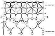
- FIG. 13a side view (looking in the ⁇ overscore (1) ⁇ 10> direction) of the atomic configuration of the Si substrate 10 , interface 14 , and single crystal oxide (specifically a alkaline-earth-metal perovskite) layer 26 is shown.
- the configuration showncomprises, in relative sizes, for illustrative purposes, from larger to smaller, barium atoms 30 , silicon atoms 32 , oxygen atoms 34 , and titanium atoms 36 .
- the Si substrate 10comprises only silicon atoms 32 .
- the interface 14comprises metal atoms (which in the preferred embodiment are illustrated as barium atoms 30 ), silicon atoms 32 , and oxygen atoms 34 .
- the single crystal oxide layer 26comprises barium atoms 30 , oxygen atoms 34 , and titanium atoms 36 .
- a top view of the interface along view line AA of FIG. 13,shows the arrangement of the barium, silicon, and oxygen atoms 30 , 32 , 34 .
- a top view along line AA of FIG. 13,shows the interface 14 and the top atomic layer 11 of the Si substrate 10 .
- a monolayerequals 6.8 ⁇ 10 14 atoms/cm 2 and an atomic layer is one atom thick.
- the interface 14 shown in the FIGs.comprises a single atomic layer, but could be more than one atomic layer, while the Si substrate 10 and the alkaline-earth-metal metal oxide layer may be many atomic layers. Note that in FIG. 13, only four atomic layers of the Si substrate 10 and only three atomic layers of the single crystal oxide layer 26 are shown.
- the interface 14comprises a half monolayer of the alkaline-earth-metal, a half monolayer of silicon, and a monolayer of oxygen.
- Each barium atom 30is substantially equally spaced from four of the silicon atoms 32 in the Si substrate 10 .
- the silicon atoms 32 in the interface 14are substantially on a line and equally spaced between the alkaline-earth-metal atoms in the ⁇ 110> direction.
- Each silicon atom 32 in the top layer of atoms in the Si substrate 10is bonded to an oxygen atom 34 in the interface 14 and each silicon atom 32 in the interface 14 is bonded to two oxygen atoms 34 in the interface 14 .
- the interface 14comprises rows of barium, silicon, and oxygen atoms 30 , 32 , 34 in a 2 ⁇ 1 configuration on a (001) surface of the Si substrate 10 , 1 ⁇ in the ⁇ overscore (1) ⁇ 10> direction and 2 ⁇ in the ⁇ 110> direction.
- the interface 14has a 2 ⁇ 1 reconstruction.
- the interface 14may comprise a single atomic layer. Better transistor applications are achieved by the interface 14 being thin, in that the electrical coupling of the overlying oxide layers to the Si substrate 10 is not compromised, and in that the interface 14 is more stable since the atoms will more likely maintain their crystalinity in processing.
Landscapes
- Chemical & Material Sciences (AREA)
- Engineering & Computer Science (AREA)
- Physics & Mathematics (AREA)
- Materials Engineering (AREA)
- Organic Chemistry (AREA)
- Metallurgy (AREA)
- Crystallography & Structural Chemistry (AREA)
- Microelectronics & Electronic Packaging (AREA)
- Computer Hardware Design (AREA)
- Power Engineering (AREA)
- Manufacturing & Machinery (AREA)
- General Physics & Mathematics (AREA)
- Condensed Matter Physics & Semiconductors (AREA)
- Chemical Kinetics & Catalysis (AREA)
- Optics & Photonics (AREA)
- General Chemical & Material Sciences (AREA)
- Inorganic Chemistry (AREA)
- Insulated Gate Type Field-Effect Transistor (AREA)
Abstract
Description
Claims (36)
Applications Claiming Priority (1)
| Application Number | Priority Date | Filing Date | Title |
|---|---|---|---|
| US27392900A | 2000-09-14 | 2000-09-14 |
Related Parent Applications (1)
| Application Number | Title | Priority Date | Filing Date |
|---|---|---|---|
| US27392900ADivision | 2000-09-14 | 2000-09-14 |
Publications (1)
| Publication Number | Publication Date |
|---|---|
| US6224669B1true US6224669B1 (en) | 2001-05-01 |
Family
ID=23046021
Family Applications (1)
| Application Number | Title | Priority Date | Filing Date |
|---|---|---|---|
| US09/662,390Expired - LifetimeUS6224669B1 (en) | 2000-09-14 | 2000-09-14 | Method for fabricating a semiconductor structure having a crystalline alkaline earth metal oxide interface with silicon |
Country Status (1)
| Country | Link |
|---|---|
| US (1) | US6224669B1 (en) |
Cited By (35)
| Publication number | Priority date | Publication date | Assignee | Title |
|---|---|---|---|---|
| US6291319B1 (en)* | 1999-12-17 | 2001-09-18 | Motorola, Inc. | Method for fabricating a semiconductor structure having a stable crystalline interface with silicon |
| US20020167070A1 (en)* | 2000-06-30 | 2002-11-14 | Motorola, Inc. | Hybrid semiconductor structure and device |
| US6493497B1 (en) | 2000-09-26 | 2002-12-10 | Motorola, Inc. | Electro-optic structure and process for fabricating same |
| US6498358B1 (en) | 2001-07-20 | 2002-12-24 | Motorola, Inc. | Structure and method for fabricating an electro-optic system having an electrochromic diffraction grating |
| US6501973B1 (en) | 2000-06-30 | 2002-12-31 | Motorola, Inc. | Apparatus and method for measuring selected physical condition of an animate subject |
| US6531740B2 (en) | 2001-07-17 | 2003-03-11 | Motorola, Inc. | Integrated impedance matching and stability network |
| US6555946B1 (en) | 2000-07-24 | 2003-04-29 | Motorola, Inc. | Acoustic wave device and process for forming the same |
| US6559471B2 (en) | 2000-12-08 | 2003-05-06 | Motorola, Inc. | Quantum well infrared photodetector and method for fabricating same |
| US6589856B2 (en) | 2001-08-06 | 2003-07-08 | Motorola, Inc. | Method and apparatus for controlling anti-phase domains in semiconductor structures and devices |
| US6590236B1 (en) | 2000-07-24 | 2003-07-08 | Motorola, Inc. | Semiconductor structure for use with high-frequency signals |
| US6638838B1 (en) | 2000-10-02 | 2003-10-28 | Motorola, Inc. | Semiconductor structure including a partially annealed layer and method of forming the same |
| US6639249B2 (en) | 2001-08-06 | 2003-10-28 | Motorola, Inc. | Structure and method for fabrication for a solid-state lighting device |
| US6646293B2 (en) | 2001-07-18 | 2003-11-11 | Motorola, Inc. | Structure for fabricating high electron mobility transistors utilizing the formation of complaint substrates |
| US6667196B2 (en) | 2001-07-25 | 2003-12-23 | Motorola, Inc. | Method for real-time monitoring and controlling perovskite oxide film growth and semiconductor structure formed using the method |
| US6673667B2 (en) | 2001-08-15 | 2004-01-06 | Motorola, Inc. | Method for manufacturing a substantially integral monolithic apparatus including a plurality of semiconductor materials |
| US6673646B2 (en) | 2001-02-28 | 2004-01-06 | Motorola, Inc. | Growth of compound semiconductor structures on patterned oxide films and process for fabricating same |
| US6693298B2 (en) | 2001-07-20 | 2004-02-17 | Motorola, Inc. | Structure and method for fabricating epitaxial semiconductor on insulator (SOI) structures and devices utilizing the formation of a compliant substrate for materials used to form same |
| US6693033B2 (en) | 2000-02-10 | 2004-02-17 | Motorola, Inc. | Method of removing an amorphous oxide from a monocrystalline surface |
| US6709989B2 (en) | 2001-06-21 | 2004-03-23 | Motorola, Inc. | Method for fabricating a semiconductor structure including a metal oxide interface with silicon |
| US6855992B2 (en) | 2001-07-24 | 2005-02-15 | Motorola Inc. | Structure and method for fabricating configurable transistor devices utilizing the formation of a compliant substrate for materials used to form the same |
| US6885065B2 (en) | 2002-11-20 | 2005-04-26 | Freescale Semiconductor, Inc. | Ferromagnetic semiconductor structure and method for forming the same |
| US6916717B2 (en) | 2002-05-03 | 2005-07-12 | Motorola, Inc. | Method for growing a monocrystalline oxide layer and for fabricating a semiconductor device on a monocrystalline substrate |
| US6965128B2 (en) | 2003-02-03 | 2005-11-15 | Freescale Semiconductor, Inc. | Structure and method for fabricating semiconductor microresonator devices |
| US6992321B2 (en) | 2001-07-13 | 2006-01-31 | Motorola, Inc. | Structure and method for fabricating semiconductor structures and devices utilizing piezoelectric materials |
| US7005717B2 (en) | 2000-05-31 | 2006-02-28 | Freescale Semiconductor, Inc. | Semiconductor device and method |
| US7019332B2 (en) | 2001-07-20 | 2006-03-28 | Freescale Semiconductor, Inc. | Fabrication of a wavelength locker within a semiconductor structure |
| US7020374B2 (en) | 2003-02-03 | 2006-03-28 | Freescale Semiconductor, Inc. | Optical waveguide structure and method for fabricating the same |
| US7045815B2 (en) | 2001-04-02 | 2006-05-16 | Freescale Semiconductor, Inc. | Semiconductor structure exhibiting reduced leakage current and method of fabricating same |
| US7067856B2 (en) | 2000-02-10 | 2006-06-27 | Freescale Semiconductor, Inc. | Semiconductor structure, semiconductor device, communicating device, integrated circuit, and process for fabricating the same |
| US7105866B2 (en) | 2000-07-24 | 2006-09-12 | Freescale Semiconductor, Inc. | Heterojunction tunneling diodes and process for fabricating same |
| US7161227B2 (en) | 2001-08-14 | 2007-01-09 | Motorola, Inc. | Structure and method for fabricating semiconductor structures and devices for detecting an object |
| US7169619B2 (en) | 2002-11-19 | 2007-01-30 | Freescale Semiconductor, Inc. | Method for fabricating semiconductor structures on vicinal substrates using a low temperature, low pressure, alkaline earth metal-rich process |
| US7211852B2 (en) | 2001-01-19 | 2007-05-01 | Freescale Semiconductor, Inc. | Structure and method for fabricating GaN devices utilizing the formation of a compliant substrate |
| US7342276B2 (en) | 2001-10-17 | 2008-03-11 | Freescale Semiconductor, Inc. | Method and apparatus utilizing monocrystalline insulator |
| EP1267408A3 (en)* | 2001-06-12 | 2009-03-04 | National Institute for Materials Science | Composite integrated circuit and its fabrication method |
Citations (13)
| Publication number | Priority date | Publication date | Assignee | Title |
|---|---|---|---|---|
| DE4120258A1 (en) | 1991-06-19 | 1992-12-24 | Siemens Ag | METHOD FOR PRODUCING A LAYER FROM A HIGH-TEMPERATURE SUPER-CONDUCTOR MATERIAL ON A SILICON SUBSTRATE |
| US5225031A (en) | 1991-04-10 | 1993-07-06 | Martin Marietta Energy Systems, Inc. | Process for depositing an oxide epitaxially onto a silicon substrate and structures prepared with the process |
| US5393352A (en) | 1992-05-01 | 1995-02-28 | Texas Instruments Incorporated | Pb/Bi-containing high-dielectric constant oxides using a non-P/Bi-containing perovskite as a buffer layer |
| US5450812A (en) | 1993-07-30 | 1995-09-19 | Martin Marietta Energy Systems, Inc. | Process for growing a film epitaxially upon an oxide surface and structures formed with the process |
| US5482003A (en) | 1991-04-10 | 1996-01-09 | Martin Marietta Energy Systems, Inc. | Process for depositing epitaxial alkaline earth oxide onto a substrate and structures prepared with the process |
| JPH0812494A (en) | 1994-06-21 | 1996-01-16 | Sharp Corp | Method of manufacturing oxide crystal thin film and thin film element |
| US5514484A (en) | 1992-11-05 | 1996-05-07 | Fuji Xerox Co., Ltd. | Oriented ferroelectric thin film |
| JPH09315897A (en) | 1996-05-31 | 1997-12-09 | Sumitomo Electric Ind Ltd | Single crystal oxide thin film having crystal type crystal structure and manufacturing method |
| US5767543A (en) | 1996-09-16 | 1998-06-16 | Motorola, Inc. | Ferroelectric semiconductor device having a layered ferroelectric structure |
| US5830270A (en) | 1996-08-05 | 1998-11-03 | Lockheed Martin Energy Systems, Inc. | CaTiO3 Interfacial template structure on semiconductor-based material and the growth of electroceramic thin-films in the perovskite class |
| US6023082A (en) | 1996-08-05 | 2000-02-08 | Lockheed Martin Energy Research Corporation | Strain-based control of crystal anisotropy for perovskite oxides on semiconductor-based material |
| US6022140A (en) | 1996-05-07 | 2000-02-08 | Braun Thermoscan | Enhanced protective lens cover for an infrared thermometer |
| US6113690A (en) | 1998-06-08 | 2000-09-05 | Motorola, Inc. | Method of preparing crystalline alkaline earth metal oxides on a Si substrate |
- 2000
- 2000-09-14USUS09/662,390patent/US6224669B1/ennot_activeExpired - Lifetime
Patent Citations (13)
| Publication number | Priority date | Publication date | Assignee | Title |
|---|---|---|---|---|
| US5225031A (en) | 1991-04-10 | 1993-07-06 | Martin Marietta Energy Systems, Inc. | Process for depositing an oxide epitaxially onto a silicon substrate and structures prepared with the process |
| US5482003A (en) | 1991-04-10 | 1996-01-09 | Martin Marietta Energy Systems, Inc. | Process for depositing epitaxial alkaline earth oxide onto a substrate and structures prepared with the process |
| DE4120258A1 (en) | 1991-06-19 | 1992-12-24 | Siemens Ag | METHOD FOR PRODUCING A LAYER FROM A HIGH-TEMPERATURE SUPER-CONDUCTOR MATERIAL ON A SILICON SUBSTRATE |
| US5393352A (en) | 1992-05-01 | 1995-02-28 | Texas Instruments Incorporated | Pb/Bi-containing high-dielectric constant oxides using a non-P/Bi-containing perovskite as a buffer layer |
| US5514484A (en) | 1992-11-05 | 1996-05-07 | Fuji Xerox Co., Ltd. | Oriented ferroelectric thin film |
| US5450812A (en) | 1993-07-30 | 1995-09-19 | Martin Marietta Energy Systems, Inc. | Process for growing a film epitaxially upon an oxide surface and structures formed with the process |
| JPH0812494A (en) | 1994-06-21 | 1996-01-16 | Sharp Corp | Method of manufacturing oxide crystal thin film and thin film element |
| US6022140A (en) | 1996-05-07 | 2000-02-08 | Braun Thermoscan | Enhanced protective lens cover for an infrared thermometer |
| JPH09315897A (en) | 1996-05-31 | 1997-12-09 | Sumitomo Electric Ind Ltd | Single crystal oxide thin film having crystal type crystal structure and manufacturing method |
| US5830270A (en) | 1996-08-05 | 1998-11-03 | Lockheed Martin Energy Systems, Inc. | CaTiO3 Interfacial template structure on semiconductor-based material and the growth of electroceramic thin-films in the perovskite class |
| US6023082A (en) | 1996-08-05 | 2000-02-08 | Lockheed Martin Energy Research Corporation | Strain-based control of crystal anisotropy for perovskite oxides on semiconductor-based material |
| US5767543A (en) | 1996-09-16 | 1998-06-16 | Motorola, Inc. | Ferroelectric semiconductor device having a layered ferroelectric structure |
| US6113690A (en) | 1998-06-08 | 2000-09-05 | Motorola, Inc. | Method of preparing crystalline alkaline earth metal oxides on a Si substrate |
Non-Patent Citations (21)
| Title |
|---|
| "A Preliminary Consideration of the Growth Behaviour of CeO2, SrTiO3 and SrVO3 films on Si Substrate", Hirotoshi Nagata, Thin Solid Films, 224(1993), pp. 1-3. |
| "A Proposal of Epitaxial Oxide Thin Film Structures for Future Oxide Electronics", M. Suzuki et al., Materials Science and Engineering B41 (1996, pp. 166-173. |
| "BaSi2 and Thin Film Alkaline Earth Silicides on Silicon", R.A. McKee et al., Appl. Phys. Lett. 63 (20), Nov. 15, 1993, pp. 2818-2820. |
| "Crystalline Oxides on Silicon: The First Five Monolayers", R.A. McKee et al., Physical Review Letters, vol. 81, No. 14, pp. 3014-3017. |
| "Effects of Buffer Layers in Epitaxial Growth of SrTiO3 Thin Film on Si(100)", Osamu Nkagawara et al., J. Appl. Phys. (1995), pp. 7226-7230. |
| "Epitaxial Growth of SrTiO3 Films on Si(100) Substrates Using a Focused Electron Beam Evaporation Method", Hiroyuki Mori et al., Jpn. J. Appl. Phys., vol. 30 (1991), pp. 1415-1417. |
| "Growth of Crystalline SrTiO3 Films on Si Substrates Using Thin Flouride Buffer Layers and Their Electrical Properties", Bum Ki Moon et al., Jpn. J. Appl. Phys., vol. 33 (1994), pp. 5911-5916. |
| "Heteroepitaxial Growth of CeO2(001) Films on Si(001) Substrates by Pulsed Laser Deposition in Ultrahigh Vacuum", Hirotoshi Nagata et al., Jpn. J. Appl. Phys., vol. 30 (1991), pp. 1136-1138. |
| "Heteroepitaxial Growth of SrO films on Si Substrates", Yuichi Kado et al., J. Appl. Phys. 61(6), 1987, pp. 2398-2400. |
| "Heteroepitaxy of Dissimilar Materials", Materials Research Society Symposium Proceedings, vol. 221, pp. 29-34. |
| "Heteroepitaxy on Silicon: Fundamentals, Structure, and Devices", Materials Research Society Symposium Proceedings, vol. 116, pp. 369-374. |
| "Molecular Beam Epitaxy Growth of Epitaxial Barium Silicide, Barium Oxide, and Barium Titanate on Silicon", R.A. McKee et al., Oak Ridge National Laboratory, 1991 American Institute of Physics, pp. 782-784. |
| "Molecular Beam Epitaxy of SrTiO3 Films on Si(100)−2 × 1 with SrO Buffer Layer", Toyokazu Tambo et al., Japanese Journal of Applied Physics, vol. 37, No. 1, pp. 4454-4459. |
| "Molecular Beam Epitaxy of SrTiO3 Films on Si(100)−2×1 with SrO Buffer Layer", Toyokazu Tambo et al., Jpn. J. Appl. Phys., vol. 37 (1998) pp. 4454-4459. |
| "Molecular Beam Epitaxy of SrTiO3 Films on Si(100)-2 x 1 with SrO Buffer Layer", Toyokazu Tambo et al., Japanese Journal of Applied Physics, vol. 37, No. 1, pp. 4454-4459. |
| "Molecular Beam Epitaxy of SrTiO3 Films on Si(100)-2x1 with SrO Buffer Layer", Toyokazu Tambo et al., Jpn. J. Appl. Phys., vol. 37 (1998) pp. 4454-4459. |
| "Roles of buffer Layers in E;itaxial Growth of SrTiO3 Films on silicon Substrates", Bum Ki Moon et al., Japanese Journal of Applied Physics, vol. 33, pp. 1742-1477. |
| "Roles of Buffer Layers in Epitaxial Growth of SrTiO3 Films on Silicon Substrates", Bum Ki Moon et al., Jpn. J. Appl. Phys., vol. 33 (1994) pp. 1472-1477. |
| "Silicon Molecular Beam Epitaxy", Materials Research Society Symposium Proceedings, vol. 220, pp. 595-600. |
| "Surface Structures and the Orthorhombic Transformation of Thin Film BaSi2 on Silicon", R. A. McKee et al., Mat. Res. Soc. Symp. Proc., vol. 221., pp. 131-136. |
| "The MBE Growth and Optical Quality of BaTiO3 and SrTiO3 Thin Films on MgO", R.A. McKee et al., Mat. Res. Soc. Symp. Proc. vol. 341, pp. 309-314. |
Cited By (35)
| Publication number | Priority date | Publication date | Assignee | Title |
|---|---|---|---|---|
| US6291319B1 (en)* | 1999-12-17 | 2001-09-18 | Motorola, Inc. | Method for fabricating a semiconductor structure having a stable crystalline interface with silicon |
| US7067856B2 (en) | 2000-02-10 | 2006-06-27 | Freescale Semiconductor, Inc. | Semiconductor structure, semiconductor device, communicating device, integrated circuit, and process for fabricating the same |
| US6693033B2 (en) | 2000-02-10 | 2004-02-17 | Motorola, Inc. | Method of removing an amorphous oxide from a monocrystalline surface |
| US7005717B2 (en) | 2000-05-31 | 2006-02-28 | Freescale Semiconductor, Inc. | Semiconductor device and method |
| US20020167070A1 (en)* | 2000-06-30 | 2002-11-14 | Motorola, Inc. | Hybrid semiconductor structure and device |
| US6501973B1 (en) | 2000-06-30 | 2002-12-31 | Motorola, Inc. | Apparatus and method for measuring selected physical condition of an animate subject |
| US6555946B1 (en) | 2000-07-24 | 2003-04-29 | Motorola, Inc. | Acoustic wave device and process for forming the same |
| US6590236B1 (en) | 2000-07-24 | 2003-07-08 | Motorola, Inc. | Semiconductor structure for use with high-frequency signals |
| US7105866B2 (en) | 2000-07-24 | 2006-09-12 | Freescale Semiconductor, Inc. | Heterojunction tunneling diodes and process for fabricating same |
| US6493497B1 (en) | 2000-09-26 | 2002-12-10 | Motorola, Inc. | Electro-optic structure and process for fabricating same |
| US6638838B1 (en) | 2000-10-02 | 2003-10-28 | Motorola, Inc. | Semiconductor structure including a partially annealed layer and method of forming the same |
| US6559471B2 (en) | 2000-12-08 | 2003-05-06 | Motorola, Inc. | Quantum well infrared photodetector and method for fabricating same |
| US7211852B2 (en) | 2001-01-19 | 2007-05-01 | Freescale Semiconductor, Inc. | Structure and method for fabricating GaN devices utilizing the formation of a compliant substrate |
| US6673646B2 (en) | 2001-02-28 | 2004-01-06 | Motorola, Inc. | Growth of compound semiconductor structures on patterned oxide films and process for fabricating same |
| US7045815B2 (en) | 2001-04-02 | 2006-05-16 | Freescale Semiconductor, Inc. | Semiconductor structure exhibiting reduced leakage current and method of fabricating same |
| EP1267408A3 (en)* | 2001-06-12 | 2009-03-04 | National Institute for Materials Science | Composite integrated circuit and its fabrication method |
| US6709989B2 (en) | 2001-06-21 | 2004-03-23 | Motorola, Inc. | Method for fabricating a semiconductor structure including a metal oxide interface with silicon |
| US6992321B2 (en) | 2001-07-13 | 2006-01-31 | Motorola, Inc. | Structure and method for fabricating semiconductor structures and devices utilizing piezoelectric materials |
| US6531740B2 (en) | 2001-07-17 | 2003-03-11 | Motorola, Inc. | Integrated impedance matching and stability network |
| US6646293B2 (en) | 2001-07-18 | 2003-11-11 | Motorola, Inc. | Structure for fabricating high electron mobility transistors utilizing the formation of complaint substrates |
| US6693298B2 (en) | 2001-07-20 | 2004-02-17 | Motorola, Inc. | Structure and method for fabricating epitaxial semiconductor on insulator (SOI) structures and devices utilizing the formation of a compliant substrate for materials used to form same |
| US6498358B1 (en) | 2001-07-20 | 2002-12-24 | Motorola, Inc. | Structure and method for fabricating an electro-optic system having an electrochromic diffraction grating |
| US7019332B2 (en) | 2001-07-20 | 2006-03-28 | Freescale Semiconductor, Inc. | Fabrication of a wavelength locker within a semiconductor structure |
| US6855992B2 (en) | 2001-07-24 | 2005-02-15 | Motorola Inc. | Structure and method for fabricating configurable transistor devices utilizing the formation of a compliant substrate for materials used to form the same |
| US6667196B2 (en) | 2001-07-25 | 2003-12-23 | Motorola, Inc. | Method for real-time monitoring and controlling perovskite oxide film growth and semiconductor structure formed using the method |
| US6589856B2 (en) | 2001-08-06 | 2003-07-08 | Motorola, Inc. | Method and apparatus for controlling anti-phase domains in semiconductor structures and devices |
| US6639249B2 (en) | 2001-08-06 | 2003-10-28 | Motorola, Inc. | Structure and method for fabrication for a solid-state lighting device |
| US7161227B2 (en) | 2001-08-14 | 2007-01-09 | Motorola, Inc. | Structure and method for fabricating semiconductor structures and devices for detecting an object |
| US6673667B2 (en) | 2001-08-15 | 2004-01-06 | Motorola, Inc. | Method for manufacturing a substantially integral monolithic apparatus including a plurality of semiconductor materials |
| US7342276B2 (en) | 2001-10-17 | 2008-03-11 | Freescale Semiconductor, Inc. | Method and apparatus utilizing monocrystalline insulator |
| US6916717B2 (en) | 2002-05-03 | 2005-07-12 | Motorola, Inc. | Method for growing a monocrystalline oxide layer and for fabricating a semiconductor device on a monocrystalline substrate |
| US7169619B2 (en) | 2002-11-19 | 2007-01-30 | Freescale Semiconductor, Inc. | Method for fabricating semiconductor structures on vicinal substrates using a low temperature, low pressure, alkaline earth metal-rich process |
| US6885065B2 (en) | 2002-11-20 | 2005-04-26 | Freescale Semiconductor, Inc. | Ferromagnetic semiconductor structure and method for forming the same |
| US7020374B2 (en) | 2003-02-03 | 2006-03-28 | Freescale Semiconductor, Inc. | Optical waveguide structure and method for fabricating the same |
| US6965128B2 (en) | 2003-02-03 | 2005-11-15 | Freescale Semiconductor, Inc. | Structure and method for fabricating semiconductor microresonator devices |
Similar Documents
| Publication | Publication Date | Title |
|---|---|---|
| US6241821B1 (en) | Method for fabricating a semiconductor structure having a crystalline alkaline earth metal oxide interface with silicon | |
| US6224669B1 (en) | Method for fabricating a semiconductor structure having a crystalline alkaline earth metal oxide interface with silicon | |
| US6248459B1 (en) | Semiconductor structure having a crystalline alkaline earth metal oxide interface with silicon | |
| US6291319B1 (en) | Method for fabricating a semiconductor structure having a stable crystalline interface with silicon | |
| EP1109212B1 (en) | Semiconductor structure having a crystalline alkaline earth metal silicon nitride/oxide interface with silicon | |
| US6270568B1 (en) | Method for fabricating a semiconductor structure with reduced leakage current density | |
| US6319730B1 (en) | Method of fabricating a semiconductor structure including a metal oxide interface | |
| US6709989B2 (en) | Method for fabricating a semiconductor structure including a metal oxide interface with silicon | |
| US6022410A (en) | Alkaline-earth metal silicides on silicon | |
| US6113690A (en) | Method of preparing crystalline alkaline earth metal oxides on a Si substrate | |
| EP1096042A1 (en) | Method for fabricating a semiconductor structure including a metal oxide interface with silicon | |
| US7364989B2 (en) | Strain control of epitaxial oxide films using virtual substrates | |
| EP1176230A1 (en) | Method of preparing crystalline alkaline earth metal oxides on an Si substrate | |
| CN1217036C (en) | Method for preparing crystalline alkaline earth metal oxide on silicon substrate | |
| HK1044627A1 (en) | Semiconductor structure having a crystallilne alkaline earth metal oxide interface with silicon | |
| HK1043246A1 (en) | Method for fabricating a semiconductor structure having a crystalline alkaline earth metal oxide interface with silicon | |
| HK1043246B (en) | Method for fabricating a semiconductor structure having a crystalline alkaline earth metal oxide interface with silicon | |
| HK1043163A1 (en) | Method of preparing crystalline alkaline earth metal oxideson a si substrate |
Legal Events
| Date | Code | Title | Description |
|---|---|---|---|
| STCF | Information on status: patent grant | Free format text:PATENTED CASE | |
| CC | Certificate of correction | ||
| CC | Certificate of correction | ||
| FEPP | Fee payment procedure | Free format text:PAYER NUMBER DE-ASSIGNED (ORIGINAL EVENT CODE: RMPN); ENTITY STATUS OF PATENT OWNER: LARGE ENTITY Free format text:PAYOR NUMBER ASSIGNED (ORIGINAL EVENT CODE: ASPN); ENTITY STATUS OF PATENT OWNER: LARGE ENTITY | |
| AS | Assignment | Owner name:FREESCALE SEMICONDUCTOR, INC., TEXAS Free format text:ASSIGNMENT OF ASSIGNORS INTEREST;ASSIGNOR:MOTOROLA, INC.;REEL/FRAME:015698/0657 Effective date:20040404 Owner name:FREESCALE SEMICONDUCTOR, INC.,TEXAS Free format text:ASSIGNMENT OF ASSIGNORS INTEREST;ASSIGNOR:MOTOROLA, INC.;REEL/FRAME:015698/0657 Effective date:20040404 | |
| FPAY | Fee payment | Year of fee payment:4 | |
| AS | Assignment | Owner name:FREESCALE SEMICONDUCTOR, INC., TEXAS Free format text:ASSIGNMENT OF ASSIGNORS INTEREST;ASSIGNOR:MOTOROLA, INC.;REEL/FRAME:015603/0299 Effective date:20041210 | |
| AS | Assignment | Owner name:CITIBANK, N.A. AS COLLATERAL AGENT, NEW YORK Free format text:SECURITY AGREEMENT;ASSIGNORS:FREESCALE SEMICONDUCTOR, INC.;FREESCALE ACQUISITION CORPORATION;FREESCALE ACQUISITION HOLDINGS CORP.;AND OTHERS;REEL/FRAME:018855/0129 Effective date:20061201 Owner name:CITIBANK, N.A. AS COLLATERAL AGENT,NEW YORK Free format text:SECURITY AGREEMENT;ASSIGNORS:FREESCALE SEMICONDUCTOR, INC.;FREESCALE ACQUISITION CORPORATION;FREESCALE ACQUISITION HOLDINGS CORP.;AND OTHERS;REEL/FRAME:018855/0129 Effective date:20061201 | |
| FEPP | Fee payment procedure | Free format text:PAYER NUMBER DE-ASSIGNED (ORIGINAL EVENT CODE: RMPN); ENTITY STATUS OF PATENT OWNER: LARGE ENTITY Free format text:PAYOR NUMBER ASSIGNED (ORIGINAL EVENT CODE: ASPN); ENTITY STATUS OF PATENT OWNER: LARGE ENTITY | |
| FPAY | Fee payment | Year of fee payment:8 | |
| AS | Assignment | Owner name:CITIBANK, N.A., AS COLLATERAL AGENT,NEW YORK Free format text:SECURITY AGREEMENT;ASSIGNOR:FREESCALE SEMICONDUCTOR, INC.;REEL/FRAME:024397/0001 Effective date:20100413 Owner name:CITIBANK, N.A., AS COLLATERAL AGENT, NEW YORK Free format text:SECURITY AGREEMENT;ASSIGNOR:FREESCALE SEMICONDUCTOR, INC.;REEL/FRAME:024397/0001 Effective date:20100413 | |
| FPAY | Fee payment | Year of fee payment:12 | |
| AS | Assignment | Owner name:CITIBANK, N.A., AS NOTES COLLATERAL AGENT, NEW YORK Free format text:SECURITY AGREEMENT;ASSIGNOR:FREESCALE SEMICONDUCTOR, INC.;REEL/FRAME:030633/0424 Effective date:20130521 Owner name:CITIBANK, N.A., AS NOTES COLLATERAL AGENT, NEW YOR Free format text:SECURITY AGREEMENT;ASSIGNOR:FREESCALE SEMICONDUCTOR, INC.;REEL/FRAME:030633/0424 Effective date:20130521 | |
| AS | Assignment | Owner name:CITIBANK, N.A., AS NOTES COLLATERAL AGENT, NEW YORK Free format text:SECURITY AGREEMENT;ASSIGNOR:FREESCALE SEMICONDUCTOR, INC.;REEL/FRAME:031591/0266 Effective date:20131101 Owner name:CITIBANK, N.A., AS NOTES COLLATERAL AGENT, NEW YOR Free format text:SECURITY AGREEMENT;ASSIGNOR:FREESCALE SEMICONDUCTOR, INC.;REEL/FRAME:031591/0266 Effective date:20131101 | |
| AS | Assignment | Owner name:FREESCALE SEMICONDUCTOR, INC., TEXAS Free format text:PATENT RELEASE;ASSIGNOR:CITIBANK, N.A., AS COLLATERAL AGENT;REEL/FRAME:037356/0143 Effective date:20151207 Owner name:FREESCALE SEMICONDUCTOR, INC., TEXAS Free format text:PATENT RELEASE;ASSIGNOR:CITIBANK, N.A., AS COLLATERAL AGENT;REEL/FRAME:037354/0225 Effective date:20151207 Owner name:FREESCALE SEMICONDUCTOR, INC., TEXAS Free format text:PATENT RELEASE;ASSIGNOR:CITIBANK, N.A., AS COLLATERAL AGENT;REEL/FRAME:037356/0553 Effective date:20151207 | |
| AS | Assignment | Owner name:MORGAN STANLEY SENIOR FUNDING, INC., MARYLAND Free format text:ASSIGNMENT AND ASSUMPTION OF SECURITY INTEREST IN PATENTS;ASSIGNOR:CITIBANK, N.A.;REEL/FRAME:037486/0517 Effective date:20151207 | |
| AS | Assignment | Owner name:MORGAN STANLEY SENIOR FUNDING, INC., MARYLAND Free format text:ASSIGNMENT AND ASSUMPTION OF SECURITY INTEREST IN PATENTS;ASSIGNOR:CITIBANK, N.A.;REEL/FRAME:037518/0292 Effective date:20151207 | |
| AS | Assignment | Owner name:MORGAN STANLEY SENIOR FUNDING, INC., MARYLAND Free format text:SUPPLEMENT TO THE SECURITY AGREEMENT;ASSIGNOR:FREESCALE SEMICONDUCTOR, INC.;REEL/FRAME:039138/0001 Effective date:20160525 | |
| AS | Assignment | Owner name:NXP, B.V., F/K/A FREESCALE SEMICONDUCTOR, INC., NETHERLANDS Free format text:RELEASE BY SECURED PARTY;ASSIGNOR:MORGAN STANLEY SENIOR FUNDING, INC.;REEL/FRAME:040925/0001 Effective date:20160912 Owner name:NXP, B.V., F/K/A FREESCALE SEMICONDUCTOR, INC., NE Free format text:RELEASE BY SECURED PARTY;ASSIGNOR:MORGAN STANLEY SENIOR FUNDING, INC.;REEL/FRAME:040925/0001 Effective date:20160912 | |
| AS | Assignment | Owner name:NXP B.V., NETHERLANDS Free format text:RELEASE BY SECURED PARTY;ASSIGNOR:MORGAN STANLEY SENIOR FUNDING, INC.;REEL/FRAME:040928/0001 Effective date:20160622 | |
| AS | Assignment | Owner name:NXP USA, INC., TEXAS Free format text:MERGER;ASSIGNOR:FREESCALE SEMICONDUCTOR, INC.;REEL/FRAME:041144/0363 Effective date:20161107 | |
| AS | Assignment | Owner name:MORGAN STANLEY SENIOR FUNDING, INC., MARYLAND Free format text:CORRECTIVE ASSIGNMENT TO CORRECT THE REMOVE PATENTS 8108266 AND 8062324 AND REPLACE THEM WITH 6108266 AND 8060324 PREVIOUSLY RECORDED ON REEL 037518 FRAME 0292. ASSIGNOR(S) HEREBY CONFIRMS THE ASSIGNMENT AND ASSUMPTION OF SECURITY INTEREST IN PATENTS;ASSIGNOR:CITIBANK, N.A.;REEL/FRAME:041703/0536 Effective date:20151207 | |
| AS | Assignment | Owner name:MOTOROLA, INC., ILLINOIS Free format text:ASSIGNMENT OF ASSIGNORS INTEREST;ASSIGNORS:YU, ZHIYI;DROOPAD, RAVINDRANATH;OVERGAARD, COREY DANIEL;AND OTHERS;SIGNING DATES FROM 19990319 TO 19990322;REEL/FRAME:043389/0734 | |
| AS | Assignment | Owner name:SHENZHEN XINGUODU TECHNOLOGY CO., LTD., CHINA Free format text:CORRECTIVE ASSIGNMENT TO CORRECT THE TO CORRECT THE APPLICATION NO. FROM 13,883,290 TO 13,833,290 PREVIOUSLY RECORDED ON REEL 041703 FRAME 0536. ASSIGNOR(S) HEREBY CONFIRMS THE THE ASSIGNMENT AND ASSUMPTION OF SECURITYINTEREST IN PATENTS.;ASSIGNOR:MORGAN STANLEY SENIOR FUNDING, INC.;REEL/FRAME:048734/0001 Effective date:20190217 | |
| AS | Assignment | Owner name:NXP B.V., NETHERLANDS Free format text:RELEASE BY SECURED PARTY;ASSIGNOR:MORGAN STANLEY SENIOR FUNDING, INC.;REEL/FRAME:050744/0097 Effective date:20190903 | |
| AS | Assignment | Owner name:MORGAN STANLEY SENIOR FUNDING, INC., MARYLAND Free format text:CORRECTIVE ASSIGNMENT TO CORRECT THE REMOVE APPLICATION11759915 AND REPLACE IT WITH APPLICATION 11759935 PREVIOUSLY RECORDED ON REEL 037486 FRAME 0517. ASSIGNOR(S) HEREBY CONFIRMS THE ASSIGNMENT AND ASSUMPTION OF SECURITYINTEREST IN PATENTS;ASSIGNOR:CITIBANK, N.A.;REEL/FRAME:053547/0421 Effective date:20151207 | |
| AS | Assignment | Owner name:NXP B.V., NETHERLANDS Free format text:CORRECTIVE ASSIGNMENT TO CORRECT THE REMOVEAPPLICATION 11759915 AND REPLACE IT WITH APPLICATION11759935 PREVIOUSLY RECORDED ON REEL 040928 FRAME 0001. ASSIGNOR(S) HEREBY CONFIRMS THE RELEASE OF SECURITYINTEREST;ASSIGNOR:MORGAN STANLEY SENIOR FUNDING, INC.;REEL/FRAME:052915/0001 Effective date:20160622 | |
| AS | Assignment | Owner name:NXP, B.V. F/K/A FREESCALE SEMICONDUCTOR, INC., NETHERLANDS Free format text:CORRECTIVE ASSIGNMENT TO CORRECT THE REMOVEAPPLICATION 11759915 AND REPLACE IT WITH APPLICATION11759935 PREVIOUSLY RECORDED ON REEL 040925 FRAME 0001. ASSIGNOR(S) HEREBY CONFIRMS THE RELEASE OF SECURITYINTEREST;ASSIGNOR:MORGAN STANLEY SENIOR FUNDING, INC.;REEL/FRAME:052917/0001 Effective date:20160912 |