US6222739B1 - High-density computer module with stacked parallel-plane packaging - Google Patents
High-density computer module with stacked parallel-plane packagingDownload PDFInfo
- Publication number
- US6222739B1 US6222739B1US09/228,867US22886799AUS6222739B1US 6222739 B1US6222739 B1US 6222739B1US 22886799 AUS22886799 AUS 22886799AUS 6222739 B1US6222739 B1US 6222739B1
- Authority
- US
- United States
- Prior art keywords
- board
- auxiliary
- primary
- module
- surface mount
- Prior art date
- Legal status (The legal status is an assumption and is not a legal conclusion. Google has not performed a legal analysis and makes no representation as to the accuracy of the status listed.)
- Expired - Lifetime
Links
Images


Classifications
- G—PHYSICS
- G06—COMPUTING OR CALCULATING; COUNTING
- G06F—ELECTRIC DIGITAL DATA PROCESSING
- G06F1/00—Details not covered by groups G06F3/00 - G06F13/00 and G06F21/00
- G06F1/16—Constructional details or arrangements
- G06F1/18—Packaging or power distribution
- G06F1/183—Internal mounting support structures, e.g. for printed circuit boards, internal connecting means
- G06F1/186—Securing of expansion boards in correspondence to slots provided at the computer enclosure
- G—PHYSICS
- G06—COMPUTING OR CALCULATING; COUNTING
- G06F—ELECTRIC DIGITAL DATA PROCESSING
- G06F1/00—Details not covered by groups G06F3/00 - G06F13/00 and G06F21/00
- G06F1/16—Constructional details or arrangements
- G06F1/18—Packaging or power distribution
- G06F1/183—Internal mounting support structures, e.g. for printed circuit boards, internal connecting means
- G06F1/184—Mounting of motherboards
- G—PHYSICS
- G06—COMPUTING OR CALCULATING; COUNTING
- G06F—ELECTRIC DIGITAL DATA PROCESSING
- G06F1/00—Details not covered by groups G06F3/00 - G06F13/00 and G06F21/00
- G06F1/16—Constructional details or arrangements
- G06F1/18—Packaging or power distribution
- G06F1/183—Internal mounting support structures, e.g. for printed circuit boards, internal connecting means
- G06F1/185—Mounting of expansion boards
- H—ELECTRICITY
- H01—ELECTRIC ELEMENTS
- H01L—SEMICONDUCTOR DEVICES NOT COVERED BY CLASS H10
- H01L25/00—Assemblies consisting of a plurality of semiconductor or other solid state devices
- H01L25/03—Assemblies consisting of a plurality of semiconductor or other solid state devices all the devices being of a type provided for in a single subclass of subclasses H10B, H10D, H10F, H10H, H10K or H10N, e.g. assemblies of rectifier diodes
- H01L25/10—Assemblies consisting of a plurality of semiconductor or other solid state devices all the devices being of a type provided for in a single subclass of subclasses H10B, H10D, H10F, H10H, H10K or H10N, e.g. assemblies of rectifier diodes the devices having separate containers
- H01L25/105—Assemblies consisting of a plurality of semiconductor or other solid state devices all the devices being of a type provided for in a single subclass of subclasses H10B, H10D, H10F, H10H, H10K or H10N, e.g. assemblies of rectifier diodes the devices having separate containers the devices being integrated devices of class H10
- H—ELECTRICITY
- H01—ELECTRIC ELEMENTS
- H01L—SEMICONDUCTOR DEVICES NOT COVERED BY CLASS H10
- H01L25/00—Assemblies consisting of a plurality of semiconductor or other solid state devices
- H01L25/16—Assemblies consisting of a plurality of semiconductor or other solid state devices the devices being of types provided for in two or more different subclasses of H10B, H10D, H10F, H10H, H10K or H10N, e.g. forming hybrid circuits
- H—ELECTRICITY
- H05—ELECTRIC TECHNIQUES NOT OTHERWISE PROVIDED FOR
- H05K—PRINTED CIRCUITS; CASINGS OR CONSTRUCTIONAL DETAILS OF ELECTRIC APPARATUS; MANUFACTURE OF ASSEMBLAGES OF ELECTRICAL COMPONENTS
- H05K1/00—Printed circuits
- H05K1/02—Details
- H05K1/14—Structural association of two or more printed circuits
- H05K1/144—Stacked arrangements of planar printed circuit boards
- H—ELECTRICITY
- H05—ELECTRIC TECHNIQUES NOT OTHERWISE PROVIDED FOR
- H05K—PRINTED CIRCUITS; CASINGS OR CONSTRUCTIONAL DETAILS OF ELECTRIC APPARATUS; MANUFACTURE OF ASSEMBLAGES OF ELECTRICAL COMPONENTS
- H05K7/00—Constructional details common to different types of electric apparatus
- H05K7/14—Mounting supporting structure in casing or on frame or rack
- H05K7/1422—Printed circuit boards receptacles, e.g. stacked structures, electronic circuit modules or box like frames
- H05K7/1427—Housings
- H05K7/1429—Housings for circuits carrying a CPU and adapted to receive expansion cards
- H05K7/1431—Retention mechanisms for CPU modules
- H—ELECTRICITY
- H01—ELECTRIC ELEMENTS
- H01L—SEMICONDUCTOR DEVICES NOT COVERED BY CLASS H10
- H01L2225/00—Details relating to assemblies covered by the group H01L25/00 but not provided for in its subgroups
- H01L2225/03—All the devices being of a type provided for in the same main group of the same subclass of class H10, e.g. assemblies of rectifier diodes
- H01L2225/10—All the devices being of a type provided for in the same main group of the same subclass of class H10, e.g. assemblies of rectifier diodes the devices having separate containers
- H01L2225/1005—All the devices being of a type provided for in the same main group of the same subclass of class H10, e.g. assemblies of rectifier diodes the devices having separate containers the devices being integrated devices of class H10
- H01L2225/1011—All the devices being of a type provided for in the same main group of the same subclass of class H10, e.g. assemblies of rectifier diodes the devices having separate containers the devices being integrated devices of class H10 the containers being in a stacked arrangement
- H01L2225/1017—All the devices being of a type provided for in the same main group of the same subclass of class H10, e.g. assemblies of rectifier diodes the devices having separate containers the devices being integrated devices of class H10 the containers being in a stacked arrangement the lowermost container comprising a device support
- H01L2225/1023—All the devices being of a type provided for in the same main group of the same subclass of class H10, e.g. assemblies of rectifier diodes the devices having separate containers the devices being integrated devices of class H10 the containers being in a stacked arrangement the lowermost container comprising a device support the support being an insulating substrate
- H—ELECTRICITY
- H01—ELECTRIC ELEMENTS
- H01L—SEMICONDUCTOR DEVICES NOT COVERED BY CLASS H10
- H01L2225/00—Details relating to assemblies covered by the group H01L25/00 but not provided for in its subgroups
- H01L2225/03—All the devices being of a type provided for in the same main group of the same subclass of class H10, e.g. assemblies of rectifier diodes
- H01L2225/10—All the devices being of a type provided for in the same main group of the same subclass of class H10, e.g. assemblies of rectifier diodes the devices having separate containers
- H01L2225/1005—All the devices being of a type provided for in the same main group of the same subclass of class H10, e.g. assemblies of rectifier diodes the devices having separate containers the devices being integrated devices of class H10
- H01L2225/1011—All the devices being of a type provided for in the same main group of the same subclass of class H10, e.g. assemblies of rectifier diodes the devices having separate containers the devices being integrated devices of class H10 the containers being in a stacked arrangement
- H01L2225/1047—Details of electrical connections between containers
- H01L2225/107—Indirect electrical connections, e.g. via an interposer, a flexible substrate, using TAB
- H—ELECTRICITY
- H01—ELECTRIC ELEMENTS
- H01L—SEMICONDUCTOR DEVICES NOT COVERED BY CLASS H10
- H01L2924/00—Indexing scheme for arrangements or methods for connecting or disconnecting semiconductor or solid-state bodies as covered by H01L24/00
- H01L2924/0001—Technical content checked by a classifier
- H01L2924/0002—Not covered by any one of groups H01L24/00, H01L24/00 and H01L2224/00
- H—ELECTRICITY
- H01—ELECTRIC ELEMENTS
- H01R—ELECTRICALLY-CONDUCTIVE CONNECTIONS; STRUCTURAL ASSOCIATIONS OF A PLURALITY OF MUTUALLY-INSULATED ELECTRICAL CONNECTING ELEMENTS; COUPLING DEVICES; CURRENT COLLECTORS
- H01R12/00—Structural associations of a plurality of mutually-insulated electrical connecting elements, specially adapted for printed circuits, e.g. printed circuit boards [PCB], flat or ribbon cables, or like generally planar structures, e.g. terminal strips, terminal blocks; Coupling devices specially adapted for printed circuits, flat or ribbon cables, or like generally planar structures; Terminals specially adapted for contact with, or insertion into, printed circuits, flat or ribbon cables, or like generally planar structures
- H01R12/70—Coupling devices
- H01R12/71—Coupling devices for rigid printing circuits or like structures
- H01R12/72—Coupling devices for rigid printing circuits or like structures coupling with the edge of the rigid printed circuits or like structures
- H01R12/721—Coupling devices for rigid printing circuits or like structures coupling with the edge of the rigid printed circuits or like structures cooperating directly with the edge of the rigid printed circuits
Definitions
- the present inventionis directed to computer memory boards and, more particularly, to expansion modules for mounting in an expansion slot of a mother board of a computer.
- Personal computersinclude a mother board for controlling the operation of the computer.
- Personal computersare sold with a specified amount of memory, for example, 1.2 gigabytes (GB) of storage memory on a hard drive and 64 megabytes (MB) of random access memory (RAM).
- GBgigabytes
- MBmegabytes
- RAMrandom access memory
- motherboardstypically include standardized expansion slots in which a memory card may be inserted.
- the expansion slotsmay also receive cards for upgrading a particular function of the computer, such as cards for sounds, video, and graphics.
- DIMM connectoris a standard industry connector for receiving a memory module. And in accordance with the “smaller-is-better” trend in the computer industry, many mother boards are equipped with only two DIMM connectors. As such, in order to install a larger amount of memory in only two DIMM connectors, higher density memory modules have been developed.
- One conventional technique for increasing the storage capacity of a memory moduleis to double the height of the module. To do so, two rows of memory chips are mounted on the memory module, essentially doubling the capacity of the module.
- One disadvantageis the double height.
- the housing of the computer and the area around the mother boardboth need to be sufficiently large in order to accommodate this doubled size of the expansion, which runs contrary to the small-is-better design principle.
- Another disadvantagelies in different trace lengths.
- a traceis the electrical conductor which connects the chips to the edge connector or interface portion of the module. In the double-row configuration, one row of chips has one trace length, and the other row of chips has another trace length.
- the trace of the further row of chipsis essentially twice as long as the closer row of chips from the edge connector. Accordingly, a signal traveling to the further rows of chips take about twice as long to arrive as the signal traveling to the closer row of chips. This arrangement requires the signal delay to be eliminated, which may be done by synchronizing the signals, which is difficult and expensive to accomplish.
- the trace of the closer row of chipsmay be physically doubled in length so that the signals arrive at the two rows at about the same time. Either solution results in a module which is limited in speed by the double-length trace.
- Another conventional technique for increasing storage capacity of a memory moduleis to configure the double-height arrangement discussed above with a foldable portion such as an integral flex conductor.
- the modulemay then be folded in half, thereby reducing the height essentially by two.
- this foldable configurationstill suffers from the drawback of the varying trace lengths.
- An additional drawbackis created by the folded arrangement in that vertical air circulation is restricted. The components of the module produce heat, and under normal convection the heated air would rise and be drawn out of the computer by a fan. However, the folded portion of the module retains heat between the folded sections, which may cause the module to function improperly and errant.
- the apparatus of the present inventionwhich provides a module for insertion into an expansion slot on a motherboard of a computer.
- Exemplary modulemaximizes the speed at which the module operates, maximizes chip density per expansion slot, and minimizes trace length.
- the module of the present inventionis particularly suitable for expanding the memory of a computer, either a desk-top, lap-top, notebook, or palm-top computer.
- an exemplary moduleincludes a primary board with an interface portion for engaging with the expansion slot.
- the interface portionmay be configured to engage with a conventional 168-pin dual in-line memory module (DIMM) connector, for example.
- DIMMdual in-line memory module
- At least one but preferably two auxiliary boardsare mounted to respective sides of the primary board.
- the auxiliary boardsare mounted with fasteners in a spaced relationship which defines an air path between each of the auxiliary boards and the primary board.
- Each of the auxiliary boardshas a trace for electrically connecting the board to the primary board.
- the air spacesallow air to circulate between the boards.
- Each of the boardsmay have a plurality of chips mounted thereon which generate heat when operating.
- the computer in which the module is insertedis a closed environment with many electronic components which also generate heat. As temperature increases, the speed of a chip decreases because of increased resistance.
- airis able to freely circulate between the boards, thereby either cooling the chips or at least providing adequate ventilation to prevent the ambient temperature from increasing undesirably.
- the primary boardhas a trace connecting the interface portion with any number of the chips that may be mounted thereon.
- the traces of the auxiliary boardshave substantially the same length, which is only slightly longer than that of the trace of the primary board.
- the traces of the module of the present inventionare substantially the same length. This feature of equal trace length advantageously eliminates the need for synchronizing signals to different rows of chips.
- the module of the inventionreduces trace length on average by about 20% to 50% over conventional arrangements or some other value consistent with operational parameters. The reduction in trace length results in a much faster operating module.
- Another aspect of the present inventionfocuses on surface mount connectors, which are a specific type of fastener, that enable the auxiliary boards to be securely mounted to respective sides of the primary boards.
- One of the advantages of the surface mount connectorsis the ease in which the auxiliary boards can be mounted and dismounted from the primary board, thus, reducing the time and costs of assembly.
- electrical failure verification and failure analysiscan be readily performed by easily separating the auxiliary boards from the primary board and interfacing the individual boards with test equipment via the surface mount connectors.
- FIG. 1is a perspective view of an exemplary embodiment of an expansion module of the present invention, particularly illustrating the expansion module mounted in an expansion slot of a mother board of a computer;
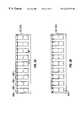
- FIG. 2is a perspective view of an exemplary expansion module of the present invention, illustrating a multiple-layer, parallel-plane configuration of boards;
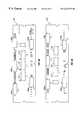
- FIG. 3Ais a side view of an auxiliary board of an expansion module of the invention, illustrating a plurality of chips mounted on a first side of the board;
- FIG. 3Bis a view similar to that of FIG. 3A, illustrating a plurality of chips mounted on a second side of the board;
- FIG. 4is a side view of a board of an exemplary expansion module of the invention, particularly highlighting a masked wiring arrangement of the board;
- FIG. 5is a cross-sectional view of an expansion module of the invention, particularly illustrating minimized trace lengths of auxiliary boards and a primary board of the module;
- FIG. 6is a cross-sectional view of an exemplary module of the invention, particularly illustrating open air paths defined between boards in a spaced relationship;
- FIG. 7is an exploded perspective view of an alternative embodiment of an expansion module of the present invention, illustrating a plurality of surface mount connectors
- FIG. 8is an exploded cross-sectional view of the expansion module illustrated in FIG. 7;
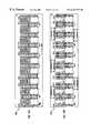
- FIG. 9Ais a side view of a primary board of the expansion module illustrated in FIG. 7, illustrating a plurality of chips and surface mount connectors mounted on a first side of the primary board;
- FIG. 9Bis a view similar to that of FIG. 9A, illustrating a plurality of chips and surface mount connectors mounted on a second side of the primary board;
- FIG. 10Ais a side view of an auxiliary board of the expansion module illustrated in FIG. 7, illustrating a plurality of chips mounted on a first side of the auxiliary board;
- FIG. 10Bis a view similar to that of FIG. 10A, illustrating a plurality of chips and surface mount connectors mounted on a second side of the auxiliary board;
- FIG. 11Ais a side view of the primary board of the expansion module shown in FIG. 7, particularly highlighting a masked wiring arrangement of the first side of the primary board;
- FIG. 11Bis a view similar to that of FIG. 11A, illustrating a masked wiring arrangement on the second side of the primary board;
- FIG. 12Ais a side view of the auxiliary board of the expansion module shown in FIG. 7, particularly highlighting a masked wiring arrangement of the first side of the auxiliary board;
- FIG. 12Bis a view similar to that of FIG. 12A, illustrating a masked wiring arrangement on the second side of the auxiliary board;
- FIG. 13Ais a top view of a male surface mount connector of the expansion module illustrated in FIG. 7;
- FIG. 13Bis a top view of a female surface mount connector of the expansion module illustrated in FIG. 7;
- FIG. 14is a cross-sectional view of the expansion module illustrated in FIG. 7, particularly illustrating minimized trace lengths of auxiliary boards of the module.
- FIG. 15is a cross-sectional view of an expansion module illustrated in FIG. 7, particularly illustrating open air paths defined between boards in a spaced relationship.
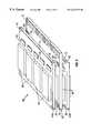
- FIG. 1an exemplary embodiment of a high-density, stacked parallel-plane module 50 and 150 of the present invention is illustrated.
- Exemplary module 50 and 150is installable in a mother board 52 of a computer 54 .
- mother board 52includes a main board 56 with a microprocessor 58 mounted thereon.
- Mother board 52may include a plurality of additional semiconductor chips and electronic components operatively associated with microprocessor 58 , which additional chips and components are not shown in the drawings for clarity.
- components and peripheral deviceswhich may be configured with computer 52 , including a monitor, input devices such as a keyboard and/or a mouse, network connections, output devices such as a printer, and so on.
- Mother board 52also includes at least one, but in general a plurality of expansion slots 60 a - 1 in communication with microprocessor 58 .
- Expansion slots 60 a - 1may respectively receive add-on modules for performing particular functions.
- a memory modulemay be inserted into one of the expansion slots 60 to increase the amount of memory of computer 54 .
- the expansion slots 60are also known in the art as connectors.
- a 168-pin dual in-line memory module (DIMM) connectoris an example of a standard expansion slot or connector commonly used in industry today.
- DIMMdual in-line memory module
- expansion slotsare referenced generally by numeral 60 , with each particular expansion slot referenced specifically by alpha suffix a, b, . . . l, respectively.
- alpha suffix a, b, . . . lalpha suffix a, b, . . . l, respectively.
- exemplary module 50 of the present inventionincludes a primary board 62 and at least one auxiliary board 64 .
- exemplary module 50includes a pair of auxiliary boards 64 a and 64 b .
- module 50 of the inventionmay include a plurality of auxiliary boards 64 a -m.
- Auxiliary boards 64are mounted to primary board 62 with fasteners 66 .
- auxiliary boards 64 a and 64 bare configured in a substantially spaced and parallel-plane relationship with respect to primary board 62 , with one of the auxiliary boards 64 being mounted on a first side of primary board 62 and the other auxiliary board 64 being mounted on a second side of primary board 62 .
- Such as relationshiphas a number of advantages, including ventilation, high density, reduced trace length, ease of manufacturing, which advantages will be discussed in more detail below.
- Exemplary boards 62 and 64may be generally configured as printed circuit boards (PCBs) or printed wiring boards (PWBs), as known in the art.
- a number of fasteners 66 or eachmay also be conductive and serve as electrical connections, which will also be discussed in more detail below.
- each board 62 and 64may include a plurality of chips 68 a -n mounted on each side thereof. Each chip 68 may perform a particular function.
- each chip 68may be a memory chip so that exemplary module 50 is a high-density memory module.
- Exemplary primary board 62includes an electrical interface portion 70 for connecting with one of the expansion slots 60 .
- each auxiliary board 64includes edge pins 72 arranged generally around a periphery thereof. Chips 68 mounted on boards 62 and/or 64 communicate with pins 72 with traces 74 .
- Boards 62 and 64may be configured with chips 68 , interface portion 70 , and pins 72 as known in the art of fabricating printed circuit boards.
- each board 62 and 64may be a multiple-layer glass epoxy configuration with interface 70 and edge pins 72 being formed by applying gold over nickel.
- Traces 74may be applied by solder masks.
- Electrical connections between auxiliary boards 64 and primary board 62may be made by fasteners 66 respectively mounted on pads 76 of primary board 62 and pads 78 of auxiliary boards 64 .
- Pads 76 of primary board 62are electrically connected to interface portion 70 (which includes a plurality of standard edge connectors as known in the art).
- Pads 78 of auxiliary boards 62are electrically connected to edge pins 72 .
- microprocessor 58may operate at increasing high speeds.
- microprocessor 58may operate on the order of hundreds of megahertz (MHz).
- expansion module 50is configured as a memory module, such as a synchronous dynamic random access memory (SDRAM)
- memory module 50needs to operate at about 100 MHz or more. Switching times at 100 MHz are on the order of 10 nanoseconds (ns).
- velocity vis substantially constant for the electrical signal (which is nearly equal to the speed of light)
- time tis substantially proportional to length l, with the length being the variable in the equation.
- trace length lneeds to be minimized.
- the velocity of the electrical signalwill vary according to temperature, in that as temperature increases, velocity decreases, which will be discuss below.
- trace length lmay be defined as the total length of the electrical connection extending from the edge connectors of interface portion 70 of primary board 62 to one of the chips 68 .
- auxiliary board 64 ahas a trace length l a
- auxiliary board 64 bhas a trace length l b , as shown by the dashed arrows.
- Exemplary module 50is configured such that trace lengths l a and l b of auxiliary boards 64 a and 64 b are substantially equal.
- auxiliary trace lengths l a and l bare only slightly longer than a trace length l p of primary board 62 , with the additional length being added by conductive fasteners 66 .
- primary trace length l pmay be increased by a small predetermined amount to be substantially equal to auxiliary trace lengths l a and l b .
- the trace lengths of the exemplary module 50may be 20% less to up to 50% less than those of conventional modules, or some other value consistent with operational parameters.
- fasteners 66 positioned along bottom edges of boards 62 and 64that is, near mother board 56 ) to serve as electrical connectors for carrying the most significant or time-dependent electrical signals from mother board 56 to auxiliary boards 64 of module 50 .
- Fasteners 66 positioned along top edges of boards 62 and 64may serve as electrical connectors for carrying less time-dependent signals, such as power, ground, and address lines, for example.
- module 50is illustrated mounted in an expansion slot 60 of a mother board 56 . (Fasteners 66 are not illustrated for clarity.) In operation, chips 68 generate heat. If the generated heat is not ventilated, then the ambient temperature around module 50 will increase, thereby decreasing the speed of the module 50 .
- the spaced parallel-plane arrangement of module 50defines an air path 80 a between auxiliary board 64 a and primary board 62 and an air path 80 b between auxiliary board 64 b and primary board 62 .
- Air paths 80are open along top and bottom edges of boards 62 and 64 .
- fasteners 66are relatively small and do not present substantial air blockage.
- Air paths 80promote circulation and allow heat (which is shown by cursive arrows and reference H) to rise and escape.
- conventional moduleshave a closed flex conductor section extending along top edges of and between a pair of boards, which prevents air circulation and traps heat between the boards, thereby greatly increasing the ambient temperature at the module and, correspondingly, decreasing the speed. Increased temperature may also cause modules to malfunction and introduce errors.
- exemplary module 50is a memory module for augmenting existing memory of computer 54 .
- chips 68may be synchronous dynamic RAM (SDRAM) chips.
- Module 50may also include a plurality of damping resistor packages 82 configured with the SDRAM chips.
- SDRAMsynchronous dynamic RAM
- One of the advantages of the memory module embodiment of the present inventionis that the amount of memory per module and memory per unit volume is maximized.
- exemplary memory module 50may include more than 256 MB for a standard 168-pin DIMM configuration. As the art of chip fabrication advances, it is obvious to those skilled in the art that more memory will be able to be included on module 50 .
- Exemplary module 150is installable in the mother board 52 of the computer 54 illustrated in FIG. 1 .
- Exemplary module 150 of the present inventionincludes a primary board 162 and at least one auxiliary board 164 .
- exemplary module 150includes a pair of auxiliary boards 164 a and 164 b .
- module 150 of the inventionmay include a plurality of auxiliary boards 164 a -m.
- Auxiliary boards 164are mounted to primary board 162 with surface mount connectors 166 such as Fine Stack connectors available from AMP.
- auxiliary boards 164 a and 164 bare configured in a substantially spaced and parallel-plane relationship with respect to primary board 162 , with one of the auxiliary boards 164 being mounted on a first side of primary board 162 and the other auxiliary board 164 being mounted on a second side of primary board 162 .
- Exemplary boards 162 and 164may be generally configured as PCBs or PWBs.
- the surface mount connectors 166also serve as electrical connections, which will be discussed in more detail below.
- primary board 162may include a plurality of chips 167 a-c mounted within an opening thereof, and with additional reference to FIGS. 10A and 10B, auxiliary boards 164 may include a plurality of chips 168 a-n mounted on each side thereof. Each chip 167 and 168 may perform a particular function such as a memory chip so that exemplary module 150 is a high-density memory module.
- Exemplary primary board 162includes an electrical interface portion 170 for connecting with one of the expansion slots 60 .
- Each surface mount connector 166includes a male surface mount connector and a matching female surface mount connector which may be easily connected and disconnected.
- Primary board 162may include five male surface mount connectors 166 a on each side thereof with three of the male surface mount connectors 166 a arranged in a single row along the top portion of the primary board 162 and the remaining two male surface mount connectors 166 b arranged in a single row along the bottom portion of the primary board 162 adjacent to the electrical interface portion 170 .
- Chips 167 mounted on primary board 162communicate with male surface mount connectors 166 a by traces 174 as shown in FIGS. 11A and 11B.
- male surface mount connectors 166 aare electrically connected to interface portion 170 of primary board 162 .
- each auxiliary board 164includes five female surface mount connectors 166 b which mechanically and electrically connect with the corresponding male surface mount connectors 166 a of primary board 162 .
- Chips 168 mounted on each of the auxiliary boards 164communicate with the female surface mount connectors 166 b by traces 174 as shown in FIGS. 12A and 12B.
- auxiliary boards 164 and primary board 162are electrically and mechanically connected by the male connectors 166 a and female connectors 166 b .
- a primary boardmay comprise fewer or more than five male surface mount connectors on each side, and each auxiliary board may correspondingly comprise fewer or more than five female connectors.
- male surface connectorsmay be mounted on auxiliary boards and female surface mount connectors may be mounted on a primary board.
- both the male connectors 166 a and female connectors 166 binclude a non-electrically conductive housing 176 .
- the housing 176encloses a plurality of electrical contacts 178 which electrically connect the male connectors 166 a to the female connectors 166 b .
- a plurality of fingers 180extend laterally and outwardly from the housing 176 .
- the male connectors 166 a and female connectors 166 beach comprise forty electrically contacts 178 and forty fingers 180 .
- the number of contacts 178 and fingers 180can range from twenty to eighty, or any other appropriate number.
- each board 162 and 164may be a multiple-layer glass epoxy configuration with traces 174 applied by solder masks.
- the auxiliary boards 164can be readily disconnected from the primary board 162 by simply separating the male connectors 166 a from their matching female connectors 166 b . By separating the boards 162 and 164 , the functionality of the boards 162 and 164 can be independently subjected to electrical failure verification and failure analysis.
- the electrical test equipmentcan be interfaced with each of the boards 162 and 164 via the surface mount connectors 166 .
- the electrical test equipmentcan include a coupling which mates with the surface mount connector, thus, replacing the costly and time consuming method of testing boards with custom bed-of-nail test fixtures.
- memory module 150may further include fastening pins 182 which provide a secondary means of mechanically connecting the primary board 162 to the auxiliary boards 164 .
- Fastening pins 182are particularly useful when the module 150 is exposed to harsh environmental conditions such as high frequency vibrations, high shock impacts, and thermal cycling.
- Each of the fastening pins 182may be fitted and soldered into openings 184 formed in each corner of the of the boards 162 and 164 .
- exemplary module 150may comprise fewer or less than four fastening pins, and the pins may be secured to the boards 162 and 164 by other means such as an adhesive or other means generally known in the art.
- trace length Lmay be defined as the total length of electrical connection extending from the edge connectors of interface portion 170 of primary board 162 to one of the chips 168 on the auxiliary board 164 .
- auxiliary board 164 ahas a trace length L a
- auxiliary board 164 bhas a trace length L b , as shown by dashed arrows.
- Exemplary module 150is configured such that trace lengths L a and L b of auxiliary boards 164 a and 164 b are substantially equal.
- surface mount connectors 166 positioned near the bottom edges of board 162 and 164that is, near mother board 56 ) to serve as electrical connectors for carrying the most significant or time-dependent electrical signals from mother board 56 to auxiliary board 164 of module 150 .
- Surface mount connectors 166 positioned near the top edges of boards 162 and 164may serve as electrical connectors for carrying less time-dependent signals, such as power, ground, and address lines, for example.
- module 150is illustrated mounted in an expansion slot 60 of a mother board 56 .
- the spaced parallel-plane arrangement of module 150is configured to promote circulation and allow heat (which is shown by cursive arrows and reference H) to rise and escape.
- the spaced parallel-plane arrangementdefines an air path 180 a between auxiliary board 164 a and primary board 162 and air path 180 b between auxiliary board 164 b and primary board 162 .
- Air paths 180are open along top and bottom edges of boards 162 and 164 , and the surface mount connectors are relatively small and do not present substantial air blockage.
- the memory module 50 and 150 shown in FIG. 1may have a thickness as defined from the outer or external side (i.e., the side not facing primary board 62 ) of one of the auxiliary boards 64 to the outer side of the other auxiliary board 64 of less than about 0.5 inch but preferably less than about 0.325 inch.
- the memory module of the present inventionmay have an overall height as defined from the bottom edge to the top edge of primary board 62 of less than about one and a half inches but preferably less than about 1.40 inches.
Landscapes
- Engineering & Computer Science (AREA)
- Microelectronics & Electronic Packaging (AREA)
- Computer Hardware Design (AREA)
- Power Engineering (AREA)
- Theoretical Computer Science (AREA)
- Physics & Mathematics (AREA)
- General Physics & Mathematics (AREA)
- General Engineering & Computer Science (AREA)
- Human Computer Interaction (AREA)
- Condensed Matter Physics & Semiconductors (AREA)
- Combinations Of Printed Boards (AREA)
- Coupling Device And Connection With Printed Circuit (AREA)
- Stackable Containers (AREA)
- Advance Control (AREA)
- Multi Processors (AREA)
- Multi-Conductor Connections (AREA)
- Printing Elements For Providing Electric Connections Between Printed Circuits (AREA)
- Cooling Or The Like Of Electrical Apparatus (AREA)
- Mounting Of Printed Circuit Boards And The Like (AREA)
Abstract
Description
Claims (43)
Priority Applications (5)
| Application Number | Priority Date | Filing Date | Title |
|---|---|---|---|
| US09/228,867US6222739B1 (en) | 1998-01-20 | 1999-01-12 | High-density computer module with stacked parallel-plane packaging |
| EP99903153AEP1050077B1 (en) | 1998-01-20 | 1999-01-19 | High-density computer modules with stacked parallel-plane packaging |
| AT99903153TATE380394T1 (en) | 1998-01-20 | 1999-01-19 | HIGH DENSITY PARALLEL STACKED COMPUTER MODULES |
| JP2000540577AJP2004507067A (en) | 1998-01-20 | 1999-01-19 | High-density computer module with stacked parallel planar packages |
| DE69937672TDE69937672T2 (en) | 1998-01-20 | 1999-01-19 | PARALLEL STACKED COMPUTER MODULES HIGH DENSITY |
Applications Claiming Priority (2)
| Application Number | Priority Date | Filing Date | Title |
|---|---|---|---|
| US892598A | 1998-01-20 | 1998-01-20 | |
| US09/228,867US6222739B1 (en) | 1998-01-20 | 1999-01-12 | High-density computer module with stacked parallel-plane packaging |
Related Parent Applications (1)
| Application Number | Title | Priority Date | Filing Date |
|---|---|---|---|
| US892598AContinuation-In-Part | 1998-01-20 | 1998-01-20 |
Publications (1)
| Publication Number | Publication Date |
|---|---|
| US6222739B1true US6222739B1 (en) | 2001-04-24 |
Family
ID=32033051
Family Applications (1)
| Application Number | Title | Priority Date | Filing Date |
|---|---|---|---|
| US09/228,867Expired - LifetimeUS6222739B1 (en) | 1998-01-20 | 1999-01-12 | High-density computer module with stacked parallel-plane packaging |
Country Status (5)
| Country | Link |
|---|---|
| US (1) | US6222739B1 (en) |
| EP (1) | EP1050077B1 (en) |
| JP (1) | JP2004507067A (en) |
| AT (1) | ATE380394T1 (en) |
| DE (1) | DE69937672T2 (en) |
Cited By (128)
| Publication number | Priority date | Publication date | Assignee | Title |
|---|---|---|---|---|
| US20020043718A1 (en)* | 2000-10-16 | 2002-04-18 | Samsung Electronics Co., | Sockets for module extension and memory system using same |
| US20020162215A1 (en)* | 2001-03-14 | 2002-11-07 | Kledzik Kenneth J. | Method and apparatus for fabricating a circuit board with a three dimensional surface mounted array of semiconductor chips |
| US20030002262A1 (en)* | 2001-07-02 | 2003-01-02 | Martin Benisek | Electronic printed circuit board having a plurality of identically designed, housing-encapsulated semiconductor memories |
| US20030151135A1 (en)* | 2000-01-31 | 2003-08-14 | Noriaki Sakamoto | Circuit device and manufacturing method of circuit device |
| US20030160317A1 (en)* | 2000-01-31 | 2003-08-28 | Noriaki Sakamoto | Circuit device and manufacturing method of circuit device and semiconductor module |
| US20030165051A1 (en)* | 2000-03-13 | 2003-09-04 | Kledzik Kenneth J. | Modular integrated circuit chip carrier |
| US20030169614A1 (en)* | 2002-03-07 | 2003-09-11 | Bhakta Jayesh R. | Arrangement of integrated ciruits in a memory module |
| US20040108590A1 (en)* | 2000-10-16 | 2004-06-10 | Kledzik Kenneth J. | Carrier-based electronic module |
| US6772261B1 (en)* | 2000-04-27 | 2004-08-03 | International Business Machines Corporation | Interface that allows testing and using memory modules in computer systems not designed for the modules |
| US20040205433A1 (en)* | 2003-04-14 | 2004-10-14 | International Business Machines Corporation | High reliability memory module with a fault tolerant address and command bus |
| US20040222784A1 (en)* | 2003-05-07 | 2004-11-11 | Chun-Nan Ou | Fixture for test cards of testing machine |
| US20050018495A1 (en)* | 2004-01-29 | 2005-01-27 | Netlist, Inc. | Arrangement of integrated circuits in a memory module |
| US6891729B2 (en)* | 2001-09-10 | 2005-05-10 | Samsung Electronics Co., Ltd. | Memory module |
| US20050225954A1 (en)* | 2004-04-09 | 2005-10-13 | Driscoll Daniel J | Field changeable graphics system for a computing device |
| US20050262455A1 (en)* | 2004-05-21 | 2005-11-24 | Hon Hai Precision Industry Co., Ltd. | System and method for verifying a layout of circuit traces on a motherboard |
| US20060034061A1 (en)* | 2004-04-01 | 2006-02-16 | Grundy Kevin P | Signal-segregating connector system |
| US20060044749A1 (en)* | 2004-04-09 | 2006-03-02 | Pauley Robert S | High density memory module using stacked printed circuit boards |
| US20060050498A1 (en)* | 2004-09-03 | 2006-03-09 | Staktek Group L.P. | Die module system and method |
| US20060053345A1 (en)* | 2004-09-03 | 2006-03-09 | Staktek Group L.P. | Thin module system and method |
| WO2005104324A3 (en)* | 2004-04-15 | 2006-03-16 | Gary W Smith | Folded, fully buffered memory module |
| US7033861B1 (en) | 2005-05-18 | 2006-04-25 | Staktek Group L.P. | Stacked module systems and method |
| US20060090102A1 (en)* | 2004-09-03 | 2006-04-27 | Wehrly James D Jr | Circuit module with thermal casing systems and methods |
| US20060107524A1 (en)* | 2000-10-16 | 2006-05-25 | Jason Engle | Method and apparatus for fabricating a circuit board with a three dimensional surface mounted array of semiconductor chips |
| US20060139983A1 (en)* | 2004-12-23 | 2006-06-29 | Sprietsma John T | Memory module routing |
| US20060137903A1 (en)* | 2004-12-23 | 2006-06-29 | Sprietsma John T | Memory module circuit board layer routing |
| US20060164820A1 (en)* | 2005-01-12 | 2006-07-27 | Mecker Donald W | Radial circuit board, system, and methods |
| US20060250780A1 (en)* | 2005-05-06 | 2006-11-09 | Staktek Group L.P. | System component interposer |
| US20060261449A1 (en)* | 2005-05-18 | 2006-11-23 | Staktek Group L.P. | Memory module system and method |
| DE102005032061A1 (en)* | 2005-07-08 | 2007-01-11 | Infineon Technologies Ag | Memory module, memory expansion memory module, memory module system, and method of manufacturing a memory module |
| US20070050530A1 (en)* | 2005-06-24 | 2007-03-01 | Rajan Suresh N | Integrated memory core and memory interface circuit |
| US20070058410A1 (en)* | 2005-09-02 | 2007-03-15 | Rajan Suresh N | Methods and apparatus of stacking DRAMs |
| US7193310B2 (en) | 2001-12-14 | 2007-03-20 | Stuktek Group L.P. | Stacking system and method |
| US7202555B2 (en) | 2001-10-26 | 2007-04-10 | Staktek Group L.P. | Pitch change and chip scale stacking system and method |
| US20070096308A1 (en)* | 2005-10-14 | 2007-05-03 | Kabushiki Kaisha Toshiba | Semiconductor device |
| US20070096302A1 (en)* | 2005-10-31 | 2007-05-03 | Josef Schuster | Semiconductor memory module |
| US20070207670A1 (en)* | 2006-02-13 | 2007-09-06 | Finisar Corporation | Optical transceiver pcb mounting system having emi containment features |
| US20070224854A1 (en)* | 2006-03-27 | 2007-09-27 | Abdallah Bacha | Memory module, method of manufacturing a memory module and computer system |
| US7289327B2 (en) | 2006-02-27 | 2007-10-30 | Stakick Group L.P. | Active cooling methods and apparatus for modules |
| US7304382B2 (en) | 2006-01-11 | 2007-12-04 | Staktek Group L.P. | Managed memory component |
| US7324352B2 (en) | 2004-09-03 | 2008-01-29 | Staktek Group L.P. | High capacity thin module system and method |
| US20080025124A1 (en)* | 2006-07-31 | 2008-01-31 | Metaram, Inc. | Interface circuit system and method for performing power management operations utilizing power management signals |
| US20080025108A1 (en)* | 2006-07-31 | 2008-01-31 | Metaram, Inc. | System and method for delaying a signal communicated from a system to at least one of a plurality of memory circuits |
| US20080025125A1 (en)* | 2006-07-31 | 2008-01-31 | Metaram, Inc. | Interface circuit system and method for performing power management operations in conjunction with only a portion of a memory circuit |
| US20080025123A1 (en)* | 2006-07-31 | 2008-01-31 | Metaram, Inc. | Interface circuit system and method for autonomously performing power management operations in conjunction with a plurality of memory circuits |
| US20080028135A1 (en)* | 2006-07-31 | 2008-01-31 | Metaram, Inc. | Multiple-component memory interface system and method |
| US20080031072A1 (en)* | 2006-07-31 | 2008-02-07 | Metaram, Inc. | Power saving system and method for use with a plurality of memory circuits |
| US20080030943A1 (en)* | 2006-08-04 | 2008-02-07 | Kyoung-Sun Kim | Memory module having improved arrangement of discrete devices |
| US20080082763A1 (en)* | 2006-10-02 | 2008-04-03 | Metaram, Inc. | Apparatus and method for power management of memory circuits by a system or component thereof |
| US20080105963A1 (en)* | 2006-07-28 | 2008-05-08 | Tessera, Inc. | Stackable electronic device assembly |
| US7443023B2 (en) | 2004-09-03 | 2008-10-28 | Entorian Technologies, Lp | High capacity thin module system |
| US7468893B2 (en) | 2004-09-03 | 2008-12-23 | Entorian Technologies, Lp | Thin module system and method |
| US7468553B2 (en) | 2006-10-20 | 2008-12-23 | Entorian Technologies, Lp | Stackable micropackages and stacked modules |
| US7480152B2 (en) | 2004-09-03 | 2009-01-20 | Entorian Technologies, Lp | Thin module system and method |
| US20090026599A1 (en)* | 2007-07-27 | 2009-01-29 | Powertech Technology Inc. | Memory module capable of lessening shock stress |
| US7508069B2 (en) | 2006-01-11 | 2009-03-24 | Entorian Technologies, Lp | Managed memory component |
| US7508058B2 (en) | 2006-01-11 | 2009-03-24 | Entorian Technologies, Lp | Stacked integrated circuit module |
| US7511969B2 (en) | 2006-02-02 | 2009-03-31 | Entorian Technologies, Lp | Composite core circuit module system and method |
| US7511968B2 (en) | 2004-09-03 | 2009-03-31 | Entorian Technologies, Lp | Buffered thin module system and method |
| US7522421B2 (en) | 2004-09-03 | 2009-04-21 | Entorian Technologies, Lp | Split core circuit module |
| EP1777998A3 (en)* | 2005-10-17 | 2009-04-22 | Alcatel Lucent | Method and apparatus for fixed and replaceable module architecture |
| DE102004039806B4 (en)* | 2003-08-13 | 2009-05-07 | Samsung Electronics Co., Ltd., Suwon | memory module |
| US7542297B2 (en) | 2004-09-03 | 2009-06-02 | Entorian Technologies, Lp | Optimized mounting area circuit module system and method |
| CN100524165C (en)* | 2006-12-05 | 2009-08-05 | 英业达股份有限公司 | Expansion structure of memory module slot |
| US7576995B2 (en) | 2005-11-04 | 2009-08-18 | Entorian Technologies, Lp | Flex circuit apparatus and method for adding capacitance while conserving circuit board surface area |
| US7581127B2 (en) | 2006-07-31 | 2009-08-25 | Metaram, Inc. | Interface circuit system and method for performing power saving operations during a command-related latency |
| US7579687B2 (en) | 2004-09-03 | 2009-08-25 | Entorian Technologies, Lp | Circuit module turbulence enhancement systems and methods |
| US7595550B2 (en) | 2001-10-26 | 2009-09-29 | Entorian Technologies, Lp | Flex-based circuit module |
| US7605454B2 (en) | 2006-01-11 | 2009-10-20 | Entorian Technologies, Lp | Memory card and method for devising |
| US7606049B2 (en) | 2004-09-03 | 2009-10-20 | Entorian Technologies, Lp | Module thermal management system and method |
| US7606040B2 (en) | 2004-09-03 | 2009-10-20 | Entorian Technologies, Lp | Memory module system and method |
| US7606050B2 (en) | 2004-09-03 | 2009-10-20 | Entorian Technologies, Lp | Compact module system and method |
| US7609567B2 (en) | 2005-06-24 | 2009-10-27 | Metaram, Inc. | System and method for simulating an aspect of a memory circuit |
| US7608920B2 (en) | 2006-01-11 | 2009-10-27 | Entorian Technologies, Lp | Memory card and method for devising |
| US7616452B2 (en) | 2004-09-03 | 2009-11-10 | Entorian Technologies, Lp | Flex circuit constructions for high capacity circuit module systems and methods |
| US7619893B1 (en) | 2006-02-17 | 2009-11-17 | Netlist, Inc. | Heat spreader for electronic modules |
| US20090284928A1 (en)* | 2008-05-13 | 2009-11-19 | Eric Alan Eckberg | Enhancing the Cooling of Dual In-Line Memory Modules |
| US7621769B1 (en) | 2004-04-09 | 2009-11-24 | Nvidia Corporation | Edge connector for field changeable graphics system |
| US7656678B2 (en) | 2001-10-26 | 2010-02-02 | Entorian Technologies, Lp | Stacked module systems |
| US7710741B1 (en) | 2005-05-03 | 2010-05-04 | Nvidia Corporation | Reconfigurable graphics processing system |
| US7724540B1 (en) | 2007-03-13 | 2010-05-25 | Yazaki North America, Inc. | Spacer for circuit boards |
| US7760513B2 (en) | 2004-09-03 | 2010-07-20 | Entorian Technologies Lp | Modified core for circuit module system and method |
| US7811097B1 (en) | 2005-08-29 | 2010-10-12 | Netlist, Inc. | Circuit with flexible portion |
| US8018723B1 (en) | 2008-04-30 | 2011-09-13 | Netlist, Inc. | Heat dissipation for electronic modules |
| US8041881B2 (en) | 2006-07-31 | 2011-10-18 | Google Inc. | Memory device with emulated characteristics |
| US8055833B2 (en) | 2006-10-05 | 2011-11-08 | Google Inc. | System and method for increasing capacity, performance, and flexibility of flash storage |
| US8060774B2 (en) | 2005-06-24 | 2011-11-15 | Google Inc. | Memory systems and memory modules |
| US8077535B2 (en) | 2006-07-31 | 2011-12-13 | Google Inc. | Memory refresh apparatus and method |
| US8081474B1 (en) | 2007-12-18 | 2011-12-20 | Google Inc. | Embossed heat spreader |
| US8080874B1 (en) | 2007-09-14 | 2011-12-20 | Google Inc. | Providing additional space between an integrated circuit and a circuit board for positioning a component therebetween |
| US8089795B2 (en) | 2006-02-09 | 2012-01-03 | Google Inc. | Memory module with memory stack and interface with enhanced capabilities |
| US8090897B2 (en) | 2006-07-31 | 2012-01-03 | Google Inc. | System and method for simulating an aspect of a memory circuit |
| US8111566B1 (en) | 2007-11-16 | 2012-02-07 | Google, Inc. | Optimal channel design for memory devices for providing a high-speed memory interface |
| US8130560B1 (en) | 2006-11-13 | 2012-03-06 | Google Inc. | Multi-rank partial width memory modules |
| US8169233B2 (en) | 2009-06-09 | 2012-05-01 | Google Inc. | Programming of DIMM termination resistance values |
| US20120106052A1 (en)* | 2010-10-29 | 2012-05-03 | Odineal Robert D | Twin-mate cpu assembly |
| US8209479B2 (en) | 2007-07-18 | 2012-06-26 | Google Inc. | Memory circuit system and method |
| US8244971B2 (en) | 2006-07-31 | 2012-08-14 | Google Inc. | Memory circuit system and method |
| US20120218698A1 (en)* | 2011-02-26 | 2012-08-30 | International Business Machines Corporation | Electronic assemblies mating system |
| US8280714B2 (en) | 2006-07-31 | 2012-10-02 | Google Inc. | Memory circuit simulation system and method with refresh capabilities |
| US8327104B2 (en) | 2006-07-31 | 2012-12-04 | Google Inc. | Adjusting the timing of signals associated with a memory system |
| US8335894B1 (en) | 2008-07-25 | 2012-12-18 | Google Inc. | Configurable memory system with interface circuit |
| US8386722B1 (en) | 2008-06-23 | 2013-02-26 | Google Inc. | Stacked DIMM memory interface |
| US8397013B1 (en) | 2006-10-05 | 2013-03-12 | Google Inc. | Hybrid memory module |
| US8438328B2 (en) | 2008-02-21 | 2013-05-07 | Google Inc. | Emulation of abstracted DIMMs using abstracted DRAMs |
| US20130181737A1 (en)* | 2012-01-13 | 2013-07-18 | Wistron Corp. | Test system and test method for pcba |
| US8566516B2 (en) | 2006-07-31 | 2013-10-22 | Google Inc. | Refresh management of memory modules |
| US8589608B2 (en) | 2011-02-26 | 2013-11-19 | International Business Machines Corporation | Logic node connection system |
| US20130313714A1 (en)* | 2012-05-22 | 2013-11-28 | Samsung Electronics Co., Ltd. | Semiconductor device having enhanced signal integrity |
| US8643657B2 (en) | 2004-04-09 | 2014-02-04 | Nvidia Corporation | Field changeable rendering system for a computing device |
| US8713228B2 (en) | 2011-02-26 | 2014-04-29 | International Business Machines Corporation | Shared system to operationally connect logic nodes |
| US8738828B2 (en) | 2011-02-26 | 2014-05-27 | International Business Machines Corporation | System to operationally connect logic nodes |
| US20140185255A1 (en)* | 2013-01-02 | 2014-07-03 | iJet Technologies, Inc. | Method to Use Empty Slots in Onboard Aircraft Servers and Communication Devices to Install Non-Proprietary Servers and Communications Interfaces |
| US8796830B1 (en) | 2006-09-01 | 2014-08-05 | Google Inc. | Stackable low-profile lead frame package |
| US9171585B2 (en) | 2005-06-24 | 2015-10-27 | Google Inc. | Configurable memory circuit system and method |
| CN105848415A (en)* | 2015-02-04 | 2016-08-10 | 乾坤科技股份有限公司 | Circuit module with surface-mount pins on side, circuit board and system |
| US9507739B2 (en) | 2005-06-24 | 2016-11-29 | Google Inc. | Configurable memory circuit system and method |
| US9542352B2 (en) | 2006-02-09 | 2017-01-10 | Google Inc. | System and method for reducing command scheduling constraints of memory circuits |
| US9632929B2 (en) | 2006-02-09 | 2017-04-25 | Google Inc. | Translating an address associated with a command communicated between a system and memory circuits |
| USD819037S1 (en)* | 2016-01-22 | 2018-05-29 | Shenzhen Longsys Electronics Co., Ltd. | SSD storage module |
| US10013371B2 (en) | 2005-06-24 | 2018-07-03 | Google Llc | Configurable memory circuit system and method |
| US10028402B1 (en)* | 2017-03-22 | 2018-07-17 | Seagate Technology Llc | Planar expansion card assembly |
| US10306751B2 (en)* | 2017-10-20 | 2019-05-28 | Hamilton Sundstrand Corporation | DDR electronic module assembly |
| US20200106201A1 (en)* | 2018-10-01 | 2020-04-02 | Te Connectivity Corporation | Board-to-board connector assembly for add-in cards |
| US11399434B2 (en)* | 2018-10-11 | 2022-07-26 | Intel Corporation | Electronic package and method of forming an electronic package |
| US20220240376A1 (en)* | 2017-01-03 | 2022-07-28 | Transportation Ip Holdings, Llc | Systems and methods for power modules |
| US20220255253A1 (en)* | 2021-02-05 | 2022-08-11 | Micro-Star Int'l Co., Limited. | Input/output transmission interface assembly and motherboard module including thereof |
| CN115119368A (en)* | 2022-07-01 | 2022-09-27 | 扬州灿阳电子科技有限公司 | Street lamp single lamp controller with 4G real-time communication function |
| CN115915583A (en)* | 2022-11-21 | 2023-04-04 | 广东工业大学 | Multilayer circuit board for computer |
Citations (21)
| Publication number | Priority date | Publication date | Assignee | Title |
|---|---|---|---|---|
| US4683550A (en)* | 1984-07-30 | 1987-07-28 | Burr-Brown Corporation | Personal computer instrumentation system including carrier board having bus-oriented plug-in instrumentation modules |
| JPH02235389A (en) | 1989-03-08 | 1990-09-18 | Mitsubishi Electric Corp | electronic circuit equipment |
| US4982265A (en) | 1987-06-24 | 1991-01-01 | Hitachi, Ltd. | Semiconductor integrated circuit device and method of manufacturing the same |
| GB2237691A (en) | 1989-10-30 | 1991-05-08 | Mitsubishi Electric Corp | Semiconductor device and wiring board module |
| JPH04206765A (en) | 1990-11-30 | 1992-07-28 | Mitsubishi Electric Corp | Semiconductor module |
| JPH04312992A (en) | 1991-03-18 | 1992-11-04 | Mitsubishi Electric Corp | Semiconductor device |
| JPH04335561A (en) | 1991-05-13 | 1992-11-24 | Mitsubishi Electric Corp | Semiconductor device |
| US5191404A (en) | 1989-12-20 | 1993-03-02 | Digital Equipment Corporation | High density memory array packaging |
| US5394300A (en) | 1992-09-04 | 1995-02-28 | Mitsubishi Denki Kabushiki Kaisha | Thin multilayered IC memory card |
| US5463249A (en)* | 1991-11-27 | 1995-10-31 | Hitachi, Ltd. | Electronic circuit system unit with wiring substrate |
| US5491612A (en) | 1995-02-21 | 1996-02-13 | Fairchild Space And Defense Corporation | Three-dimensional modular assembly of integrated circuits |
| US5495397A (en) | 1993-04-27 | 1996-02-27 | International Business Machines Corporation | Three dimensional package and architecture for high performance computer |
| US5548486A (en) | 1994-01-21 | 1996-08-20 | International Business Machines Corporation | Pinned module |
| US5583749A (en) | 1994-11-30 | 1996-12-10 | Altera Corporation | Baseboard and daughtercard apparatus for reconfigurable computing systems |
| US5616962A (en)* | 1992-01-24 | 1997-04-01 | Kabushiki Kaisha Toshiba | Semiconductor integrated circuit devices having particular terminal geometry |
| US5636997A (en) | 1993-07-06 | 1997-06-10 | Hitachi Maxell, Ltd. | Connection apparatus of circuit board |
| US5754408A (en) | 1995-11-29 | 1998-05-19 | Mitsubishi Semiconductor America, Inc. | Stackable double-density integrated circuit assemblies |
| US5754409A (en)* | 1996-11-06 | 1998-05-19 | Dynamem, Inc. | Foldable electronic assembly module |
| US5842874A (en)* | 1994-05-25 | 1998-12-01 | Molex Incorporated | Dual housing board-to-board connector |
| US5949657A (en)* | 1997-12-01 | 1999-09-07 | Karabatsos; Chris | Bottom or top jumpered foldable electronic assembly |
| US6038132A (en)* | 1996-12-06 | 2000-03-14 | Mitsubishi Denki Kabushiki Kaisha | Memory module |
- 1999
- 1999-01-12USUS09/228,867patent/US6222739B1/ennot_activeExpired - Lifetime
- 1999-01-19JPJP2000540577Apatent/JP2004507067A/enactivePending
- 1999-01-19EPEP99903153Apatent/EP1050077B1/ennot_activeExpired - Lifetime
- 1999-01-19ATAT99903153Tpatent/ATE380394T1/ennot_activeIP Right Cessation
- 1999-01-19DEDE69937672Tpatent/DE69937672T2/ennot_activeExpired - Lifetime
Patent Citations (21)
| Publication number | Priority date | Publication date | Assignee | Title |
|---|---|---|---|---|
| US4683550A (en)* | 1984-07-30 | 1987-07-28 | Burr-Brown Corporation | Personal computer instrumentation system including carrier board having bus-oriented plug-in instrumentation modules |
| US4982265A (en) | 1987-06-24 | 1991-01-01 | Hitachi, Ltd. | Semiconductor integrated circuit device and method of manufacturing the same |
| JPH02235389A (en) | 1989-03-08 | 1990-09-18 | Mitsubishi Electric Corp | electronic circuit equipment |
| GB2237691A (en) | 1989-10-30 | 1991-05-08 | Mitsubishi Electric Corp | Semiconductor device and wiring board module |
| US5191404A (en) | 1989-12-20 | 1993-03-02 | Digital Equipment Corporation | High density memory array packaging |
| JPH04206765A (en) | 1990-11-30 | 1992-07-28 | Mitsubishi Electric Corp | Semiconductor module |
| JPH04312992A (en) | 1991-03-18 | 1992-11-04 | Mitsubishi Electric Corp | Semiconductor device |
| JPH04335561A (en) | 1991-05-13 | 1992-11-24 | Mitsubishi Electric Corp | Semiconductor device |
| US5463249A (en)* | 1991-11-27 | 1995-10-31 | Hitachi, Ltd. | Electronic circuit system unit with wiring substrate |
| US5616962A (en)* | 1992-01-24 | 1997-04-01 | Kabushiki Kaisha Toshiba | Semiconductor integrated circuit devices having particular terminal geometry |
| US5394300A (en) | 1992-09-04 | 1995-02-28 | Mitsubishi Denki Kabushiki Kaisha | Thin multilayered IC memory card |
| US5495397A (en) | 1993-04-27 | 1996-02-27 | International Business Machines Corporation | Three dimensional package and architecture for high performance computer |
| US5636997A (en) | 1993-07-06 | 1997-06-10 | Hitachi Maxell, Ltd. | Connection apparatus of circuit board |
| US5548486A (en) | 1994-01-21 | 1996-08-20 | International Business Machines Corporation | Pinned module |
| US5842874A (en)* | 1994-05-25 | 1998-12-01 | Molex Incorporated | Dual housing board-to-board connector |
| US5583749A (en) | 1994-11-30 | 1996-12-10 | Altera Corporation | Baseboard and daughtercard apparatus for reconfigurable computing systems |
| US5491612A (en) | 1995-02-21 | 1996-02-13 | Fairchild Space And Defense Corporation | Three-dimensional modular assembly of integrated circuits |
| US5754408A (en) | 1995-11-29 | 1998-05-19 | Mitsubishi Semiconductor America, Inc. | Stackable double-density integrated circuit assemblies |
| US5754409A (en)* | 1996-11-06 | 1998-05-19 | Dynamem, Inc. | Foldable electronic assembly module |
| US6038132A (en)* | 1996-12-06 | 2000-03-14 | Mitsubishi Denki Kabushiki Kaisha | Memory module |
| US5949657A (en)* | 1997-12-01 | 1999-09-07 | Karabatsos; Chris | Bottom or top jumpered foldable electronic assembly |
Cited By (247)
| Publication number | Priority date | Publication date | Assignee | Title |
|---|---|---|---|---|
| US7091606B2 (en)* | 2000-01-31 | 2006-08-15 | Sanyo Electric Co., Ltd. | Circuit device and manufacturing method of circuit device and semiconductor module |
| US20030151135A1 (en)* | 2000-01-31 | 2003-08-14 | Noriaki Sakamoto | Circuit device and manufacturing method of circuit device |
| US20030160317A1 (en)* | 2000-01-31 | 2003-08-28 | Noriaki Sakamoto | Circuit device and manufacturing method of circuit device and semiconductor module |
| US7125798B2 (en) | 2000-01-31 | 2006-10-24 | Sanyo Electric Co., Ltd. | Circuit device and manufacturing method of circuit device |
| US20050056916A1 (en)* | 2000-01-31 | 2005-03-17 | Sanyo Electric Co., Ltd., A Japan Corporation | Circuit device and manufacturing method of circuit device |
| US20060254809A1 (en)* | 2000-03-13 | 2006-11-16 | Kledzik Kenneth J | Modular integrated circuit chip carrier |
| US20030165051A1 (en)* | 2000-03-13 | 2003-09-04 | Kledzik Kenneth J. | Modular integrated circuit chip carrier |
| US7102892B2 (en) | 2000-03-13 | 2006-09-05 | Legacy Electronics, Inc. | Modular integrated circuit chip carrier |
| US7796400B2 (en) | 2000-03-13 | 2010-09-14 | Legacy Electronics, Inc. | Modular integrated circuit chip carrier |
| US6772261B1 (en)* | 2000-04-27 | 2004-08-03 | International Business Machines Corporation | Interface that allows testing and using memory modules in computer systems not designed for the modules |
| US20060107524A1 (en)* | 2000-10-16 | 2006-05-25 | Jason Engle | Method and apparatus for fabricating a circuit board with a three dimensional surface mounted array of semiconductor chips |
| US7045891B2 (en)* | 2000-10-16 | 2006-05-16 | Samsung Electronic Co., Ltd. | Sockets for module extension and memory system using same |
| US20040108590A1 (en)* | 2000-10-16 | 2004-06-10 | Kledzik Kenneth J. | Carrier-based electronic module |
| US7337522B2 (en) | 2000-10-16 | 2008-03-04 | Legacy Electronics, Inc. | Method and apparatus for fabricating a circuit board with a three dimensional surface mounted array of semiconductor chips |
| US20020043718A1 (en)* | 2000-10-16 | 2002-04-18 | Samsung Electronics Co., | Sockets for module extension and memory system using same |
| US6976848B2 (en) | 2000-10-16 | 2005-12-20 | Samsung Electronics Co., Ltd. | Sockets for module extension and memory system using same |
| US7405471B2 (en)* | 2000-10-16 | 2008-07-29 | Legacy Electronics, Inc. | Carrier-based electronic module |
| US20050083664A1 (en)* | 2000-10-16 | 2005-04-21 | Samsung Electronics Co., Ltd. | Sockets for module extension and memory system using same |
| US7316060B2 (en) | 2001-03-14 | 2008-01-08 | Legacy Electronics, Inc. | System for populating a circuit board with semiconductor chips |
| US20040194301A1 (en)* | 2001-03-14 | 2004-10-07 | Kledzik Kenneth J. | Method and apparatus for fabricating a circuit board with a three dimensional surface mounted array of semiconductor chips |
| US20020162215A1 (en)* | 2001-03-14 | 2002-11-07 | Kledzik Kenneth J. | Method and apparatus for fabricating a circuit board with a three dimensional surface mounted array of semiconductor chips |
| US7103970B2 (en) | 2001-03-14 | 2006-09-12 | Legacy Electronics, Inc. | Method for fabricating a circuit board with a three dimensional surface mounted array of semiconductor chips |
| US20030002262A1 (en)* | 2001-07-02 | 2003-01-02 | Martin Benisek | Electronic printed circuit board having a plurality of identically designed, housing-encapsulated semiconductor memories |
| US6850414B2 (en)* | 2001-07-02 | 2005-02-01 | Infineon Technologies Ag | Electronic printed circuit board having a plurality of identically designed, housing-encapsulated semiconductor memories |
| US6891729B2 (en)* | 2001-09-10 | 2005-05-10 | Samsung Electronics Co., Ltd. | Memory module |
| US7595550B2 (en) | 2001-10-26 | 2009-09-29 | Entorian Technologies, Lp | Flex-based circuit module |
| US7656678B2 (en) | 2001-10-26 | 2010-02-02 | Entorian Technologies, Lp | Stacked module systems |
| US7202555B2 (en) | 2001-10-26 | 2007-04-10 | Staktek Group L.P. | Pitch change and chip scale stacking system and method |
| US7193310B2 (en) | 2001-12-14 | 2007-03-20 | Stuktek Group L.P. | Stacking system and method |
| US20040184299A1 (en)* | 2002-03-07 | 2004-09-23 | Bhakta Jayesh R. | Arrangement of integrated circuits in a memory module |
| US6873534B2 (en) | 2002-03-07 | 2005-03-29 | Netlist, Inc. | Arrangement of integrated circuits in a memory module |
| US20040057269A1 (en)* | 2002-03-07 | 2004-03-25 | Bhakta Jayesh R. | Arrangement of integrated circuits in a memory module |
| US6930900B2 (en) | 2002-03-07 | 2005-08-16 | Netlist, Inc. | Arrangement of integrated circuits in a memory module |
| US6930903B2 (en) | 2002-03-07 | 2005-08-16 | Netlist, Inc. | Arrangement of integrated circuits in a memory module |
| US20030169614A1 (en)* | 2002-03-07 | 2003-09-11 | Bhakta Jayesh R. | Arrangement of integrated ciruits in a memory module |
| WO2003077132A1 (en)* | 2002-03-07 | 2003-09-18 | Netlist, Inc. | Arrangement of integrated circuits in a memory module |
| US20040184301A1 (en)* | 2002-03-07 | 2004-09-23 | Bhakta Jayesh R. | Arrangement of integrated circuits in a memory module |
| US20040136229A1 (en)* | 2002-03-07 | 2004-07-15 | Bhakta Jayesh R. | Arrangement of integrated circuits in a memory module |
| US6751113B2 (en)* | 2002-03-07 | 2004-06-15 | Netlist, Inc. | Arrangement of integrated circuits in a memory module |
| US7761771B2 (en) | 2003-04-14 | 2010-07-20 | International Business Machines Corporation | High reliability memory module with a fault tolerant address and command bus |
| US8489936B2 (en) | 2003-04-14 | 2013-07-16 | International Business Machines Corporation | High reliability memory module with a fault tolerant address and command bus |
| US20040205433A1 (en)* | 2003-04-14 | 2004-10-14 | International Business Machines Corporation | High reliability memory module with a fault tolerant address and command bus |
| US7380179B2 (en) | 2003-04-14 | 2008-05-27 | International Business Machines Corporation | High reliability memory module with a fault tolerant address and command bus |
| US20060190780A1 (en)* | 2003-04-14 | 2006-08-24 | Gower Kevin C | High reliability memory module with a fault tolerant address and command bus |
| US7363533B2 (en) | 2003-04-14 | 2008-04-22 | International Business Machines Corporation | High reliability memory module with a fault tolerant address and command bus |
| US7234099B2 (en)* | 2003-04-14 | 2007-06-19 | International Business Machines Corporation | High reliability memory module with a fault tolerant address and command bus |
| US7366947B2 (en) | 2003-04-14 | 2008-04-29 | International Business Machines Corporation | High reliability memory module with a fault tolerant address and command bus |
| US20060242541A1 (en)* | 2003-04-14 | 2006-10-26 | Gower Kevin C | High reliability memory module with a fault tolerant address and command bus |
| US20070204201A1 (en)* | 2003-04-14 | 2007-08-30 | International Business Machines Corporation | High reliability memory module with a fault tolerant address and command bus |
| US20070204200A1 (en)* | 2003-04-14 | 2007-08-30 | International Business Machines Corporation | High reliability memory module with a fault tolerant address and command bus |
| US20070250756A1 (en)* | 2003-04-14 | 2007-10-25 | Gower Kevin C | High reliability memory module with a fault tolerant address and command bus |
| US20040222784A1 (en)* | 2003-05-07 | 2004-11-11 | Chun-Nan Ou | Fixture for test cards of testing machine |
| US6828777B2 (en)* | 2003-05-07 | 2004-12-07 | Hon Hai Precidion Ind. Co., Ltd | Fixture for test cards of testing machine |
| DE102004039806B4 (en)* | 2003-08-13 | 2009-05-07 | Samsung Electronics Co., Ltd., Suwon | memory module |
| US20050018495A1 (en)* | 2004-01-29 | 2005-01-27 | Netlist, Inc. | Arrangement of integrated circuits in a memory module |
| US20070236901A1 (en)* | 2004-04-01 | 2007-10-11 | Grundy Kevin P | Signal-Segregating Connector System |
| US20060034061A1 (en)* | 2004-04-01 | 2006-02-16 | Grundy Kevin P | Signal-segregating connector system |
| US7613011B2 (en) | 2004-04-01 | 2009-11-03 | Interconnect Portfolio Llc | Signal-segregating connector system |
| US7227759B2 (en)* | 2004-04-01 | 2007-06-05 | Silicon Pipe, Inc. | Signal-segregating connector system |
| US20050225954A1 (en)* | 2004-04-09 | 2005-10-13 | Driscoll Daniel J | Field changeable graphics system for a computing device |
| US20080316712A1 (en)* | 2004-04-09 | 2008-12-25 | Pauley Robert S | High density module having at least two substrates and at least one thermally conductive layer therebetween |
| US8643657B2 (en) | 2004-04-09 | 2014-02-04 | Nvidia Corporation | Field changeable rendering system for a computing device |
| US7839645B2 (en) | 2004-04-09 | 2010-11-23 | Netlist, Inc. | Module having at least two surfaces and at least one thermally conductive layer therebetween |
| US7254036B2 (en)* | 2004-04-09 | 2007-08-07 | Netlist, Inc. | High density memory module using stacked printed circuit boards |
| US7170757B2 (en)* | 2004-04-09 | 2007-01-30 | Nvidia Corporation | Field changeable graphics system for a computing device |
| US20110110047A1 (en)* | 2004-04-09 | 2011-05-12 | Netlist, Inc. | Module having at least two surfaces and at least one thermally conductive layer therebetween |
| US7630202B2 (en) | 2004-04-09 | 2009-12-08 | Netlist, Inc. | High density module having at least two substrates and at least one thermally conductive layer therebetween |
| US7621769B1 (en) | 2004-04-09 | 2009-11-24 | Nvidia Corporation | Edge connector for field changeable graphics system |
| US8345427B2 (en) | 2004-04-09 | 2013-01-01 | Netlist, Inc. | Module having at least two surfaces and at least one thermally conductive layer therebetween |
| US8971045B1 (en)* | 2004-04-09 | 2015-03-03 | Netlist, Inc. | Module having at least one thermally conductive layer between printed circuit boards |
| US20100110642A1 (en)* | 2004-04-09 | 2010-05-06 | Netlist, Inc. | Module having at least two surfaces and at least one thermally conductive layer therebetween |
| US20060044749A1 (en)* | 2004-04-09 | 2006-03-02 | Pauley Robert S | High density memory module using stacked printed circuit boards |
| WO2005104324A3 (en)* | 2004-04-15 | 2006-03-16 | Gary W Smith | Folded, fully buffered memory module |
| US20050262455A1 (en)* | 2004-05-21 | 2005-11-24 | Hon Hai Precision Industry Co., Ltd. | System and method for verifying a layout of circuit traces on a motherboard |
| US7219318B2 (en)* | 2004-05-21 | 2007-05-15 | Hong Fu Jin Precision Industry (Shenzhen) Co., Ltd. | System and method for verifying a layout of circuit traces on a motherboard |
| US7443023B2 (en) | 2004-09-03 | 2008-10-28 | Entorian Technologies, Lp | High capacity thin module system |
| US7606049B2 (en) | 2004-09-03 | 2009-10-20 | Entorian Technologies, Lp | Module thermal management system and method |
| US7626259B2 (en) | 2004-09-03 | 2009-12-01 | Entorian Technologies, Lp | Heat sink for a high capacity thin module system |
| US7324352B2 (en) | 2004-09-03 | 2008-01-29 | Staktek Group L.P. | High capacity thin module system and method |
| US7616452B2 (en) | 2004-09-03 | 2009-11-10 | Entorian Technologies, Lp | Flex circuit constructions for high capacity circuit module systems and methods |
| US7760513B2 (en) | 2004-09-03 | 2010-07-20 | Entorian Technologies Lp | Modified core for circuit module system and method |
| US7606050B2 (en) | 2004-09-03 | 2009-10-20 | Entorian Technologies, Lp | Compact module system and method |
| US20060090102A1 (en)* | 2004-09-03 | 2006-04-27 | Wehrly James D Jr | Circuit module with thermal casing systems and methods |
| US7606042B2 (en) | 2004-09-03 | 2009-10-20 | Entorian Technologies, Lp | High capacity thin module system and method |
| US7579687B2 (en) | 2004-09-03 | 2009-08-25 | Entorian Technologies, Lp | Circuit module turbulence enhancement systems and methods |
| US7522425B2 (en) | 2004-09-03 | 2009-04-21 | Entorian Technologies, Lp | High capacity thin module system and method |
| US7522421B2 (en) | 2004-09-03 | 2009-04-21 | Entorian Technologies, Lp | Split core circuit module |
| US7606040B2 (en) | 2004-09-03 | 2009-10-20 | Entorian Technologies, Lp | Memory module system and method |
| US7542297B2 (en) | 2004-09-03 | 2009-06-02 | Entorian Technologies, Lp | Optimized mounting area circuit module system and method |
| US20060053345A1 (en)* | 2004-09-03 | 2006-03-09 | Staktek Group L.P. | Thin module system and method |
| US7602613B2 (en) | 2004-09-03 | 2009-10-13 | Entorian Technologies, Lp | Thin module system and method |
| US20060050498A1 (en)* | 2004-09-03 | 2006-03-09 | Staktek Group L.P. | Die module system and method |
| US7768796B2 (en) | 2004-09-03 | 2010-08-03 | Entorian Technologies L.P. | Die module system |
| US7511968B2 (en) | 2004-09-03 | 2009-03-31 | Entorian Technologies, Lp | Buffered thin module system and method |
| US7423885B2 (en) | 2004-09-03 | 2008-09-09 | Entorian Technologies, Lp | Die module system |
| US7480152B2 (en) | 2004-09-03 | 2009-01-20 | Entorian Technologies, Lp | Thin module system and method |
| US7737549B2 (en) | 2004-09-03 | 2010-06-15 | Entorian Technologies Lp | Circuit module with thermal casing systems |
| US7468893B2 (en) | 2004-09-03 | 2008-12-23 | Entorian Technologies, Lp | Thin module system and method |
| US7446410B2 (en) | 2004-09-03 | 2008-11-04 | Entorian Technologies, Lp | Circuit module with thermal casing systems |
| US7459784B2 (en) | 2004-09-03 | 2008-12-02 | Entorian Technologies, Lp | High capacity thin module system |
| US20080266778A1 (en)* | 2004-12-23 | 2008-10-30 | Intel Corporation | Memory module routing |
| US20060137903A1 (en)* | 2004-12-23 | 2006-06-29 | Sprietsma John T | Memory module circuit board layer routing |
| US20060139983A1 (en)* | 2004-12-23 | 2006-06-29 | Sprietsma John T | Memory module routing |
| US20060164820A1 (en)* | 2005-01-12 | 2006-07-27 | Mecker Donald W | Radial circuit board, system, and methods |
| US7435097B2 (en) | 2005-01-12 | 2008-10-14 | Legacy Electronics, Inc. | Radial circuit board, system, and methods |
| US7710741B1 (en) | 2005-05-03 | 2010-05-04 | Nvidia Corporation | Reconfigurable graphics processing system |
| US20060250780A1 (en)* | 2005-05-06 | 2006-11-09 | Staktek Group L.P. | System component interposer |
| US20060261449A1 (en)* | 2005-05-18 | 2006-11-23 | Staktek Group L.P. | Memory module system and method |
| US7033861B1 (en) | 2005-05-18 | 2006-04-25 | Staktek Group L.P. | Stacked module systems and method |
| US9171585B2 (en) | 2005-06-24 | 2015-10-27 | Google Inc. | Configurable memory circuit system and method |
| US8615679B2 (en) | 2005-06-24 | 2013-12-24 | Google Inc. | Memory modules with reliability and serviceability functions |
| US7515453B2 (en) | 2005-06-24 | 2009-04-07 | Metaram, Inc. | Integrated memory core and memory interface circuit |
| US20070050530A1 (en)* | 2005-06-24 | 2007-03-01 | Rajan Suresh N | Integrated memory core and memory interface circuit |
| US10013371B2 (en) | 2005-06-24 | 2018-07-03 | Google Llc | Configurable memory circuit system and method |
| US9507739B2 (en) | 2005-06-24 | 2016-11-29 | Google Inc. | Configurable memory circuit system and method |
| US7609567B2 (en) | 2005-06-24 | 2009-10-27 | Metaram, Inc. | System and method for simulating an aspect of a memory circuit |
| US8060774B2 (en) | 2005-06-24 | 2011-11-15 | Google Inc. | Memory systems and memory modules |
| US8359187B2 (en) | 2005-06-24 | 2013-01-22 | Google Inc. | Simulating a different number of memory circuit devices |
| US8386833B2 (en) | 2005-06-24 | 2013-02-26 | Google Inc. | Memory systems and memory modules |
| DE102005032061B4 (en)* | 2005-07-08 | 2009-07-30 | Qimonda Ag | Memory module, and memory module system |
| DE102005032061A1 (en)* | 2005-07-08 | 2007-01-11 | Infineon Technologies Ag | Memory module, memory expansion memory module, memory module system, and method of manufacturing a memory module |
| US20070015381A1 (en)* | 2005-07-08 | 2007-01-18 | Simon Muff | Memory module, memory extension memory module, memory module system, and method for manufacturing a memory module |
| US7351072B2 (en) | 2005-07-08 | 2008-04-01 | Qimonda Ag | Memory module, memory extension memory module, memory module system, and method for manufacturing a memory module |
| US8033836B1 (en) | 2005-08-29 | 2011-10-11 | Netlist, Inc. | Circuit with flexible portion |
| US7811097B1 (en) | 2005-08-29 | 2010-10-12 | Netlist, Inc. | Circuit with flexible portion |
| US8864500B1 (en) | 2005-08-29 | 2014-10-21 | Netlist, Inc. | Electronic module with flexible portion |
| US20070058410A1 (en)* | 2005-09-02 | 2007-03-15 | Rajan Suresh N | Methods and apparatus of stacking DRAMs |
| US8619452B2 (en) | 2005-09-02 | 2013-12-31 | Google Inc. | Methods and apparatus of stacking DRAMs |
| US7379316B2 (en) | 2005-09-02 | 2008-05-27 | Metaram, Inc. | Methods and apparatus of stacking DRAMs |
| US8582339B2 (en) | 2005-09-02 | 2013-11-12 | Google Inc. | System including memory stacks |
| US8811065B2 (en) | 2005-09-02 | 2014-08-19 | Google Inc. | Performing error detection on DRAMs |
| US8040682B2 (en)* | 2005-10-14 | 2011-10-18 | Kabushiki Kaisha Toshiba | Semiconductor device |
| US20070096308A1 (en)* | 2005-10-14 | 2007-05-03 | Kabushiki Kaisha Toshiba | Semiconductor device |
| US8769808B2 (en) | 2005-10-17 | 2014-07-08 | Alcatel Lucent | Method for fixed and replaceable module architecture |
| EP1777998A3 (en)* | 2005-10-17 | 2009-04-22 | Alcatel Lucent | Method and apparatus for fixed and replaceable module architecture |
| CN1953652B (en)* | 2005-10-17 | 2011-03-30 | 阿尔卡特公司 | Method and device for fixed and replaceable modular structures |
| US7315454B2 (en)* | 2005-10-31 | 2008-01-01 | Infineon Technologies Ag | Semiconductor memory module |
| US20070096302A1 (en)* | 2005-10-31 | 2007-05-03 | Josef Schuster | Semiconductor memory module |
| US7576995B2 (en) | 2005-11-04 | 2009-08-18 | Entorian Technologies, Lp | Flex circuit apparatus and method for adding capacitance while conserving circuit board surface area |
| US7605454B2 (en) | 2006-01-11 | 2009-10-20 | Entorian Technologies, Lp | Memory card and method for devising |
| US7608920B2 (en) | 2006-01-11 | 2009-10-27 | Entorian Technologies, Lp | Memory card and method for devising |
| US7304382B2 (en) | 2006-01-11 | 2007-12-04 | Staktek Group L.P. | Managed memory component |
| US7508069B2 (en) | 2006-01-11 | 2009-03-24 | Entorian Technologies, Lp | Managed memory component |
| US7508058B2 (en) | 2006-01-11 | 2009-03-24 | Entorian Technologies, Lp | Stacked integrated circuit module |
| US7511969B2 (en) | 2006-02-02 | 2009-03-31 | Entorian Technologies, Lp | Composite core circuit module system and method |
| US9542352B2 (en) | 2006-02-09 | 2017-01-10 | Google Inc. | System and method for reducing command scheduling constraints of memory circuits |
| US8089795B2 (en) | 2006-02-09 | 2012-01-03 | Google Inc. | Memory module with memory stack and interface with enhanced capabilities |
| US9727458B2 (en) | 2006-02-09 | 2017-08-08 | Google Inc. | Translating an address associated with a command communicated between a system and memory circuits |
| US9632929B2 (en) | 2006-02-09 | 2017-04-25 | Google Inc. | Translating an address associated with a command communicated between a system and memory circuits |
| US8797779B2 (en) | 2006-02-09 | 2014-08-05 | Google Inc. | Memory module with memory stack and interface with enhanced capabilites |
| US9542353B2 (en) | 2006-02-09 | 2017-01-10 | Google Inc. | System and method for reducing command scheduling constraints of memory circuits |
| US8566556B2 (en) | 2006-02-09 | 2013-10-22 | Google Inc. | Memory module with memory stack and interface with enhanced capabilities |
| WO2007095554A3 (en)* | 2006-02-13 | 2008-05-22 | Finisar Corp | Optical transceiver pcb mounting system having emi containment features |
| US20070207670A1 (en)* | 2006-02-13 | 2007-09-06 | Finisar Corporation | Optical transceiver pcb mounting system having emi containment features |
| US7481656B2 (en) | 2006-02-13 | 2009-01-27 | Finisar Corporation | Optical transceiver PCB mounting system having EMI containment features |
| US7619893B1 (en) | 2006-02-17 | 2009-11-17 | Netlist, Inc. | Heat spreader for electronic modules |
| US7839643B1 (en) | 2006-02-17 | 2010-11-23 | Netlist, Inc. | Heat spreader for memory modules |
| US8488325B1 (en) | 2006-02-17 | 2013-07-16 | Netlist, Inc. | Memory module having thermal conduits |
| US7289327B2 (en) | 2006-02-27 | 2007-10-30 | Stakick Group L.P. | Active cooling methods and apparatus for modules |
| US20070224854A1 (en)* | 2006-03-27 | 2007-09-27 | Abdallah Bacha | Memory module, method of manufacturing a memory module and computer system |
| US20080105963A1 (en)* | 2006-07-28 | 2008-05-08 | Tessera, Inc. | Stackable electronic device assembly |
| US7580312B2 (en) | 2006-07-31 | 2009-08-25 | Metaram, Inc. | Power saving system and method for use with a plurality of memory circuits |
| US7386656B2 (en) | 2006-07-31 | 2008-06-10 | Metaram, Inc. | Interface circuit system and method for performing power management operations in conjunction with only a portion of a memory circuit |
| US20080025124A1 (en)* | 2006-07-31 | 2008-01-31 | Metaram, Inc. | Interface circuit system and method for performing power management operations utilizing power management signals |
| US20080025108A1 (en)* | 2006-07-31 | 2008-01-31 | Metaram, Inc. | System and method for delaying a signal communicated from a system to at least one of a plurality of memory circuits |
| US8631220B2 (en) | 2006-07-31 | 2014-01-14 | Google Inc. | Adjusting the timing of signals associated with a memory system |
| US8090897B2 (en) | 2006-07-31 | 2012-01-03 | Google Inc. | System and method for simulating an aspect of a memory circuit |
| US20080025125A1 (en)* | 2006-07-31 | 2008-01-31 | Metaram, Inc. | Interface circuit system and method for performing power management operations in conjunction with only a portion of a memory circuit |
| US7581127B2 (en) | 2006-07-31 | 2009-08-25 | Metaram, Inc. | Interface circuit system and method for performing power saving operations during a command-related latency |
| US8154935B2 (en) | 2006-07-31 | 2012-04-10 | Google Inc. | Delaying a signal communicated from a system to at least one of a plurality of memory circuits |
| US20080025123A1 (en)* | 2006-07-31 | 2008-01-31 | Metaram, Inc. | Interface circuit system and method for autonomously performing power management operations in conjunction with a plurality of memory circuits |
| US20080028135A1 (en)* | 2006-07-31 | 2008-01-31 | Metaram, Inc. | Multiple-component memory interface system and method |
| US20080031072A1 (en)* | 2006-07-31 | 2008-02-07 | Metaram, Inc. | Power saving system and method for use with a plurality of memory circuits |
| US8244971B2 (en) | 2006-07-31 | 2012-08-14 | Google Inc. | Memory circuit system and method |
| US7472220B2 (en) | 2006-07-31 | 2008-12-30 | Metaram, Inc. | Interface circuit system and method for performing power management operations utilizing power management signals |
| US8280714B2 (en) | 2006-07-31 | 2012-10-02 | Google Inc. | Memory circuit simulation system and method with refresh capabilities |
| US8327104B2 (en) | 2006-07-31 | 2012-12-04 | Google Inc. | Adjusting the timing of signals associated with a memory system |
| US9047976B2 (en) | 2006-07-31 | 2015-06-02 | Google Inc. | Combined signal delay and power saving for use with a plurality of memory circuits |
| US8340953B2 (en) | 2006-07-31 | 2012-12-25 | Google, Inc. | Memory circuit simulation with power saving capabilities |
| US8041881B2 (en) | 2006-07-31 | 2011-10-18 | Google Inc. | Memory device with emulated characteristics |
| US7590796B2 (en) | 2006-07-31 | 2009-09-15 | Metaram, Inc. | System and method for power management in memory systems |
| US7392338B2 (en) | 2006-07-31 | 2008-06-24 | Metaram, Inc. | Interface circuit system and method for autonomously performing power management operations in conjunction with a plurality of memory circuits |
| US8566516B2 (en) | 2006-07-31 | 2013-10-22 | Google Inc. | Refresh management of memory modules |
| US8077535B2 (en) | 2006-07-31 | 2011-12-13 | Google Inc. | Memory refresh apparatus and method |
| US8745321B2 (en) | 2006-07-31 | 2014-06-03 | Google Inc. | Simulating a memory standard |
| US8972673B2 (en) | 2006-07-31 | 2015-03-03 | Google Inc. | Power management of memory circuits by virtual memory simulation |
| US8868829B2 (en) | 2006-07-31 | 2014-10-21 | Google Inc. | Memory circuit system and method |
| US7724589B2 (en) | 2006-07-31 | 2010-05-25 | Google Inc. | System and method for delaying a signal communicated from a system to at least one of a plurality of memory circuits |
| US20080030943A1 (en)* | 2006-08-04 | 2008-02-07 | Kyoung-Sun Kim | Memory module having improved arrangement of discrete devices |
| US8796830B1 (en) | 2006-09-01 | 2014-08-05 | Google Inc. | Stackable low-profile lead frame package |
| US20080082763A1 (en)* | 2006-10-02 | 2008-04-03 | Metaram, Inc. | Apparatus and method for power management of memory circuits by a system or component thereof |
| US8055833B2 (en) | 2006-10-05 | 2011-11-08 | Google Inc. | System and method for increasing capacity, performance, and flexibility of flash storage |
| US8397013B1 (en) | 2006-10-05 | 2013-03-12 | Google Inc. | Hybrid memory module |
| US8370566B2 (en) | 2006-10-05 | 2013-02-05 | Google Inc. | System and method for increasing capacity, performance, and flexibility of flash storage |
| US8977806B1 (en) | 2006-10-05 | 2015-03-10 | Google Inc. | Hybrid memory module |
| US8751732B2 (en) | 2006-10-05 | 2014-06-10 | Google Inc. | System and method for increasing capacity, performance, and flexibility of flash storage |
| US7468553B2 (en) | 2006-10-20 | 2008-12-23 | Entorian Technologies, Lp | Stackable micropackages and stacked modules |
| US8760936B1 (en) | 2006-11-13 | 2014-06-24 | Google Inc. | Multi-rank partial width memory modules |
| US8130560B1 (en) | 2006-11-13 | 2012-03-06 | Google Inc. | Multi-rank partial width memory modules |
| US8446781B1 (en) | 2006-11-13 | 2013-05-21 | Google Inc. | Multi-rank partial width memory modules |
| CN100524165C (en)* | 2006-12-05 | 2009-08-05 | 英业达股份有限公司 | Expansion structure of memory module slot |
| US7724540B1 (en) | 2007-03-13 | 2010-05-25 | Yazaki North America, Inc. | Spacer for circuit boards |
| US8209479B2 (en) | 2007-07-18 | 2012-06-26 | Google Inc. | Memory circuit system and method |
| US20090026599A1 (en)* | 2007-07-27 | 2009-01-29 | Powertech Technology Inc. | Memory module capable of lessening shock stress |
| US8080874B1 (en) | 2007-09-14 | 2011-12-20 | Google Inc. | Providing additional space between an integrated circuit and a circuit board for positioning a component therebetween |
| US8675429B1 (en) | 2007-11-16 | 2014-03-18 | Google Inc. | Optimal channel design for memory devices for providing a high-speed memory interface |
| US8111566B1 (en) | 2007-11-16 | 2012-02-07 | Google, Inc. | Optimal channel design for memory devices for providing a high-speed memory interface |
| US8730670B1 (en) | 2007-12-18 | 2014-05-20 | Google Inc. | Embossed heat spreader |
| US8081474B1 (en) | 2007-12-18 | 2011-12-20 | Google Inc. | Embossed heat spreader |
| US8705240B1 (en) | 2007-12-18 | 2014-04-22 | Google Inc. | Embossed heat spreader |
| US8631193B2 (en) | 2008-02-21 | 2014-01-14 | Google Inc. | Emulation of abstracted DIMMS using abstracted DRAMS |
| US8438328B2 (en) | 2008-02-21 | 2013-05-07 | Google Inc. | Emulation of abstracted DIMMs using abstracted DRAMs |
| US8018723B1 (en) | 2008-04-30 | 2011-09-13 | Netlist, Inc. | Heat dissipation for electronic modules |
| US8705239B1 (en) | 2008-04-30 | 2014-04-22 | Netlist, Inc. | Heat dissipation for electronic modules |
| US7684196B2 (en)* | 2008-05-13 | 2010-03-23 | International Business Machines Corporation | Enhancing the cooling of dual in-line memory modules |
| US20090284928A1 (en)* | 2008-05-13 | 2009-11-19 | Eric Alan Eckberg | Enhancing the Cooling of Dual In-Line Memory Modules |
| US8386722B1 (en) | 2008-06-23 | 2013-02-26 | Google Inc. | Stacked DIMM memory interface |
| US8762675B2 (en) | 2008-06-23 | 2014-06-24 | Google Inc. | Memory system for synchronous data transmission |
| US8819356B2 (en) | 2008-07-25 | 2014-08-26 | Google Inc. | Configurable multirank memory system with interface circuit |
| US8335894B1 (en) | 2008-07-25 | 2012-12-18 | Google Inc. | Configurable memory system with interface circuit |
| US8169233B2 (en) | 2009-06-09 | 2012-05-01 | Google Inc. | Programming of DIMM termination resistance values |
| US20120106052A1 (en)* | 2010-10-29 | 2012-05-03 | Odineal Robert D | Twin-mate cpu assembly |
| US8589608B2 (en) | 2011-02-26 | 2013-11-19 | International Business Machines Corporation | Logic node connection system |
| US8597032B2 (en)* | 2011-02-26 | 2013-12-03 | International Business Machines Corporation | Electronic assemblies mating system |
| US20120218698A1 (en)* | 2011-02-26 | 2012-08-30 | International Business Machines Corporation | Electronic assemblies mating system |
| US8738828B2 (en) | 2011-02-26 | 2014-05-27 | International Business Machines Corporation | System to operationally connect logic nodes |
| US8713228B2 (en) | 2011-02-26 | 2014-04-29 | International Business Machines Corporation | Shared system to operationally connect logic nodes |
| US20130181737A1 (en)* | 2012-01-13 | 2013-07-18 | Wistron Corp. | Test system and test method for pcba |
| US9013204B2 (en)* | 2012-01-13 | 2015-04-21 | Wistron Corp. | Test system and test method for PCBA |
| US20130313714A1 (en)* | 2012-05-22 | 2013-11-28 | Samsung Electronics Co., Ltd. | Semiconductor device having enhanced signal integrity |
| US20140185255A1 (en)* | 2013-01-02 | 2014-07-03 | iJet Technologies, Inc. | Method to Use Empty Slots in Onboard Aircraft Servers and Communication Devices to Install Non-Proprietary Servers and Communications Interfaces |
| CN105848415A (en)* | 2015-02-04 | 2016-08-10 | 乾坤科技股份有限公司 | Circuit module with surface-mount pins on side, circuit board and system |
| CN105848415B (en)* | 2015-02-04 | 2020-06-16 | 乾坤科技股份有限公司 | Circuit module with surface-mount pins on side, circuit board and system |
| US9668359B2 (en)* | 2015-02-04 | 2017-05-30 | Cyntec Co., Ltd. | Circuit module having surface-mount pads on a lateral surface for connecting with a circuit board |
| USD819037S1 (en)* | 2016-01-22 | 2018-05-29 | Shenzhen Longsys Electronics Co., Ltd. | SSD storage module |
| US20220240376A1 (en)* | 2017-01-03 | 2022-07-28 | Transportation Ip Holdings, Llc | Systems and methods for power modules |
| US12225657B2 (en)* | 2017-01-03 | 2025-02-11 | Transportation Ip Holdings, Llc | Power system and method for controlling power modules |
| US10028402B1 (en)* | 2017-03-22 | 2018-07-17 | Seagate Technology Llc | Planar expansion card assembly |
| US10306751B2 (en)* | 2017-10-20 | 2019-05-28 | Hamilton Sundstrand Corporation | DDR electronic module assembly |
| US10903594B2 (en)* | 2018-10-01 | 2021-01-26 | Te Connectivity Corporation | Board-to-board connector assembly for add-in cards |
| US20200106201A1 (en)* | 2018-10-01 | 2020-04-02 | Te Connectivity Corporation | Board-to-board connector assembly for add-in cards |
| US11399434B2 (en)* | 2018-10-11 | 2022-07-26 | Intel Corporation | Electronic package and method of forming an electronic package |
| US20220255253A1 (en)* | 2021-02-05 | 2022-08-11 | Micro-Star Int'l Co., Limited. | Input/output transmission interface assembly and motherboard module including thereof |
| US11742603B2 (en)* | 2021-02-05 | 2023-08-29 | Micro-Star Int'l Co., Limited. | Input/output transmission interface assembly and motherboard module including thereof |
| CN115119368A (en)* | 2022-07-01 | 2022-09-27 | 扬州灿阳电子科技有限公司 | Street lamp single lamp controller with 4G real-time communication function |
| CN115119368B (en)* | 2022-07-01 | 2023-09-12 | 扬州灿阳电子科技有限公司 | Street lamp single lamp controller with 4G real-time communication function |
| CN115915583A (en)* | 2022-11-21 | 2023-04-04 | 广东工业大学 | Multilayer circuit board for computer |
Also Published As
| Publication number | Publication date |
|---|---|
| DE69937672T2 (en) | 2008-11-13 |
| DE69937672D1 (en) | 2008-01-17 |
| EP1050077A4 (en) | 2002-07-31 |
| EP1050077A1 (en) | 2000-11-08 |
| JP2004507067A (en) | 2004-03-04 |
| EP1050077B1 (en) | 2007-12-05 |
| ATE380394T1 (en) | 2007-12-15 |
Similar Documents
| Publication | Publication Date | Title |
|---|---|---|
| US6222739B1 (en) | High-density computer module with stacked parallel-plane packaging | |
| US6160718A (en) | Multi-chip package with stacked chips and interconnect bumps | |
| US6762942B1 (en) | Break away, high speed, folded, jumperless electronic assembly | |
| US7737549B2 (en) | Circuit module with thermal casing systems | |
| US7235880B2 (en) | IC package with power and signal lines on opposing sides | |
| US7606049B2 (en) | Module thermal management system and method | |
| US6021048A (en) | High speed memory module | |
| US5825630A (en) | Electronic circuit board including a second circuit board attached there to to provide an area of increased circuit density | |
| US7542297B2 (en) | Optimized mounting area circuit module system and method | |
| US7446410B2 (en) | Circuit module with thermal casing systems | |
| US5951665A (en) | Interface optimized computer system architecture | |
| US20060049512A1 (en) | Thin module system and method with skew reduction | |
| US20060050492A1 (en) | Thin module system and method | |
| US7863089B2 (en) | Planar array contact memory cards | |
| US20060050592A1 (en) | Compact module system and method | |
| US6381140B1 (en) | Memory module | |
| US7269025B2 (en) | Ballout for buffer | |
| US5816826A (en) | Computer circuit board with direct connect peripheral slot assembly | |
| US7212408B2 (en) | Multi-slot socket for mounting integrated circuits on circuit board | |
| JP2006074031A (en) | Circuit module system and method | |
| US6288908B1 (en) | Peripheral apparatus for PC cards | |
| WO1999036959A9 (en) | High-density computer modules with stacked parallel-plane packaging | |
| US6094355A (en) | High-density computer modules with double-layer packaging | |
| US20020075662A1 (en) | Stack-type expansible electronic device | |
| HK1121287A1 (en) | Memory module system and method |
Legal Events
| Date | Code | Title | Description |
|---|---|---|---|
| AS | Assignment | Owner name:VIKING COMPONENTS, CALIFORNIA Free format text:ASSIGNMENT OF ASSIGNORS INTEREST;ASSIGNORS:BHATKA, JAYESH R.;VAKILIAN, KAVOUS;REEL/FRAME:009701/0399;SIGNING DATES FROM 19990104 TO 19990105 | |
| STCF | Information on status: patent grant | Free format text:PATENTED CASE | |
| AS | Assignment | Owner name:THE CIT GROUP/BUSINESS CREDIT, INC., CALIFORNIA Free format text:SECURITY AGREEMENT;ASSIGNOR:VIKING COMPONENTS INCORPORATED;REEL/FRAME:012153/0627 Effective date:20010913 | |
| AS | Assignment | Owner name:VIKING COMPONENTS INCORPORATED, CALIFORNIA Free format text:RELEASE OF SECURITY INTEREST RECORDED ON 09/19/2001 AT REEL/FRAME 012153/0627;ASSIGNOR:CIT GROUP/BUSINESS CREDIT, INC.;REEL/FRAME:013333/0528 Effective date:20030102 | |
| AS | Assignment | Owner name:LASALLE BUSINESS CREDIT, INC., AS COLLATERAL AGENT Free format text:PLEDGE AND SECURITY AGREEMENT;ASSIGNORS:SANMINA-SCI CORPORATION;COMPATIBLE MEMORY, INC.;ESSEX ACQUISITION SUBSIDIARY, INC.;AND OTHERS;REEL/FRAME:013362/0374 Effective date:20021223 | |
| AS | Assignment | Owner name:COMPATIBLE MEMORY, INC., CALIFORNIA Free format text:TERMINATION OF SECURITY INTEREST IN PATENTS;ASSIGNOR:LASALLE BUSINESS CREDIT, LLC (SUCCESSOR BY MERGER TO LASALLE BUSINESS CREDIT, INC.), AS COLLATERAL AGENT;REEL/FRAME:014289/0558 Effective date:20030922 Owner name:ESSEX ACQUISITION SUBSIDIARY, INC., CALIFORNIA Free format text:TERMINATION OF SECURITY INTEREST IN PATENTS;ASSIGNOR:LASALLE BUSINESS CREDIT, LLC (SUCCESSOR BY MERGER TO LASALLE BUSINESS CREDIT, INC.), AS COLLATERAL AGENT;REEL/FRAME:014289/0558 Effective date:20030922 Owner name:HADCO CORPORATION, CALIFORNIA Free format text:TERMINATION OF SECURITY INTEREST IN PATENTS;ASSIGNOR:LASALLE BUSINESS CREDIT, LLC (SUCCESSOR BY MERGER TO LASALLE BUSINESS CREDIT, INC.), AS COLLATERAL AGENT;REEL/FRAME:014289/0558 Effective date:20030922 Owner name:HADCO SANTA CLARA, INC., CALIFORNIA Free format text:TERMINATION OF SECURITY INTEREST IN PATENTS;ASSIGNOR:LASALLE BUSINESS CREDIT, LLC (SUCCESSOR BY MERGER TO LASALLE BUSINESS CREDIT, INC.), AS COLLATERAL AGENT;REEL/FRAME:014289/0558 Effective date:20030922 Owner name:INTERAGENCY, INC., CALIFORNIA Free format text:TERMINATION OF SECURITY INTEREST IN PATENTS;ASSIGNOR:LASALLE BUSINESS CREDIT, LLC (SUCCESSOR BY MERGER TO LASALLE BUSINESS CREDIT, INC.), AS COLLATERAL AGENT;REEL/FRAME:014289/0558 Effective date:20030922 Owner name:INTERWORKS COMPUTER PRODUCTS, CALIFORNIA Free format text:TERMINATION OF SECURITY INTEREST IN PATENTS;ASSIGNOR:LASALLE BUSINESS CREDIT, LLC (SUCCESSOR BY MERGER TO LASALLE BUSINESS CREDIT, INC.), AS COLLATERAL AGENT;REEL/FRAME:014289/0558 Effective date:20030922 Owner name:MANU-TRONICS, INC., CALIFORNIA Free format text:TERMINATION OF SECURITY INTEREST IN PATENTS;ASSIGNOR:LASALLE BUSINESS CREDIT, LLC (SUCCESSOR BY MERGER TO LASALLE BUSINESS CREDIT, INC.), AS COLLATERAL AGENT;REEL/FRAME:014289/0558 Effective date:20030922 Owner name:MOOSE ACQUISITION SUBSIDIARY, INC., CALIFORNIA Free format text:TERMINATION OF SECURITY INTEREST IN PATENTS;ASSIGNOR:LASALLE BUSINESS CREDIT, LLC (SUCCESSOR BY MERGER TO LASALLE BUSINESS CREDIT, INC.), AS COLLATERAL AGENT;REEL/FRAME:014289/0558 Effective date:20030922 Owner name:SANMINA CANADA HOLDINGS, INC., CALIFORNIA Free format text:TERMINATION OF SECURITY INTEREST IN PATENTS;ASSIGNOR:LASALLE BUSINESS CREDIT, LLC (SUCCESSOR BY MERGER TO LASALLE BUSINESS CREDIT, INC.), AS COLLATERAL AGENT;REEL/FRAME:014289/0558 Effective date:20030922 Owner name:SANMINA ENCLOSURE SYSTEMS USA INC., CALIFORNIA Free format text:TERMINATION OF SECURITY INTEREST IN PATENTS;ASSIGNOR:LASALLE BUSINESS CREDIT, LLC (SUCCESSOR BY MERGER TO LASALLE BUSINESS CREDIT, INC.), AS COLLATERAL AGENT;REEL/FRAME:014289/0558 Effective date:20030922 Owner name:SANMINA-SCI CORPORATION, CALIFORNIA Free format text:TERMINATION OF SECURITY INTEREST IN PATENTS;ASSIGNOR:LASALLE BUSINESS CREDIT, LLC (SUCCESSOR BY MERGER TO LASALLE BUSINESS CREDIT, INC.), AS COLLATERAL AGENT;REEL/FRAME:014289/0558 Effective date:20030922 Owner name:SANMINA-SCI SYSTEMS (ALABAMA) INC., CALIFORNIA Free format text:TERMINATION OF SECURITY INTEREST IN PATENTS;ASSIGNOR:LASALLE BUSINESS CREDIT, LLC (SUCCESSOR BY MERGER TO LASALLE BUSINESS CREDIT, INC.), AS COLLATERAL AGENT;REEL/FRAME:014289/0558 Effective date:20030922 Owner name:SANMINA-SCI SYSTEMS ENCLOSURES, LLC, CALIFORNIA Free format text:TERMINATION OF SECURITY INTEREST IN PATENTS;ASSIGNOR:LASALLE BUSINESS CREDIT, LLC (SUCCESSOR BY MERGER TO LASALLE BUSINESS CREDIT, INC.), AS COLLATERAL AGENT;REEL/FRAME:014289/0558 Effective date:20030922 Owner name:SCI ENCLOSURES (DENTON), INC., CALIFORNIA Free format text:TERMINATION OF SECURITY INTEREST IN PATENTS;ASSIGNOR:LASALLE BUSINESS CREDIT, LLC (SUCCESSOR BY MERGER TO LASALLE BUSINESS CREDIT, INC.), AS COLLATERAL AGENT;REEL/FRAME:014289/0558 Effective date:20030922 Owner name:SCI HOLDINGS, INC., CALIFORNIA Free format text:TERMINATION OF SECURITY INTEREST IN PATENTS;ASSIGNOR:LASALLE BUSINESS CREDIT, LLC (SUCCESSOR BY MERGER TO LASALLE BUSINESS CREDIT, INC.), AS COLLATERAL AGENT;REEL/FRAME:014289/0558 Effective date:20030922 Owner name:SCI SYSTEMS, INC., CALIFORNIA Free format text:TERMINATION OF SECURITY INTEREST IN PATENTS;ASSIGNOR:LASALLE BUSINESS CREDIT, LLC (SUCCESSOR BY MERGER TO LASALLE BUSINESS CREDIT, INC.), AS COLLATERAL AGENT;REEL/FRAME:014289/0558 Effective date:20030922 Owner name:SCI TECHNOLOGY, INC., CALIFORNIA Free format text:TERMINATION OF SECURITY INTEREST IN PATENTS;ASSIGNOR:LASALLE BUSINESS CREDIT, LLC (SUCCESSOR BY MERGER TO LASALLE BUSINESS CREDIT, INC.), AS COLLATERAL AGENT;REEL/FRAME:014289/0558 Effective date:20030922 Owner name:SCIMEX, INC., CALIFORNIA Free format text:TERMINATION OF SECURITY INTEREST IN PATENTS;ASSIGNOR:LASALLE BUSINESS CREDIT, LLC (SUCCESSOR BY MERGER TO LASALLE BUSINESS CREDIT, INC.), AS COLLATERAL AGENT;REEL/FRAME:014289/0558 Effective date:20030922 Owner name:VIKING COMPONENTS INCORPORATED, CALIFORNIA Free format text:TERMINATION OF SECURITY INTEREST IN PATENTS;ASSIGNOR:LASALLE BUSINESS CREDIT, LLC (SUCCESSOR BY MERGER TO LASALLE BUSINESS CREDIT, INC.), AS COLLATERAL AGENT;REEL/FRAME:014289/0558 Effective date:20030922 | |
| AS | Assignment | Owner name:COMPATIBLE MEMORY, INC., CALIFORNIA Free format text:TERMINATION OF SECURITY INTEREST IN PATENTS;ASSIGNOR:LASALLE BUSINESS CREDIT, LLC (SUCCESSOR BY MERGER TO LASALLE BUSINESS CREDIT, INC.), COLLATERAL AGENT;REEL/FRAME:014462/0678 Effective date:20030922 Owner name:ESSEX ACQUISITION SUBSIDIARY, INC., CALIFORNIA Free format text:TERMINATION OF SECURITY INTEREST IN PATENTS;ASSIGNOR:LASALLE BUSINESS CREDIT, LLC (SUCCESSOR BY MERGER TO LASALLE BUSINESS CREDIT, INC.), COLLATERAL AGENT;REEL/FRAME:014462/0678 Effective date:20030922 Owner name:HADCO CORPORATION, CALIFORNIA Free format text:TERMINATION OF SECURITY INTEREST IN PATENTS;ASSIGNOR:LASALLE BUSINESS CREDIT, LLC (SUCCESSOR BY MERGER TO LASALLE BUSINESS CREDIT, INC.), COLLATERAL AGENT;REEL/FRAME:014462/0678 Effective date:20030922 Owner name:HADCO SANTA CLARA, INC., CALIFORNIA Free format text:TERMINATION OF SECURITY INTEREST IN PATENTS;ASSIGNOR:LASALLE BUSINESS CREDIT, LLC (SUCCESSOR BY MERGER TO LASALLE BUSINESS CREDIT, INC.), COLLATERAL AGENT;REEL/FRAME:014462/0678 Effective date:20030922 Owner name:INTERAGENCY, INC., CALIFORNIA Free format text:TERMINATION OF SECURITY INTEREST IN PATENTS;ASSIGNOR:LASALLE BUSINESS CREDIT, LLC (SUCCESSOR BY MERGER TO LASALLE BUSINESS CREDIT, INC.), COLLATERAL AGENT;REEL/FRAME:014462/0678 Effective date:20030922 Owner name:INTERWORKS COMPUTER PRODUCTS, CALIFORNIA Free format text:TERMINATION OF SECURITY INTEREST IN PATENTS;ASSIGNOR:LASALLE BUSINESS CREDIT, LLC (SUCCESSOR BY MERGER TO LASALLE BUSINESS CREDIT, INC.), COLLATERAL AGENT;REEL/FRAME:014462/0678 Effective date:20030922 Owner name:MANU-TRONICS, INC., CALIFORNIA Free format text:TERMINATION OF SECURITY INTEREST IN PATENTS;ASSIGNOR:LASALLE BUSINESS CREDIT, LLC (SUCCESSOR BY MERGER TO LASALLE BUSINESS CREDIT, INC.), COLLATERAL AGENT;REEL/FRAME:014462/0678 Effective date:20030922 Owner name:MOOSE ACQUISITION SUBSIDIARY, INC., CALIFORNIA Free format text:TERMINATION OF SECURITY INTEREST IN PATENTS;ASSIGNOR:LASALLE BUSINESS CREDIT, LLC (SUCCESSOR BY MERGER TO LASALLE BUSINESS CREDIT, INC.), COLLATERAL AGENT;REEL/FRAME:014462/0678 Effective date:20030922 Owner name:NEWISYS, INC., CALIFORNIA Free format text:TERMINATION OF SECURITY INTEREST IN PATENTS;ASSIGNOR:LASALLE BUSINESS CREDIT, LLC (SUCCESSOR BY MERGER TO LASALLE BUSINESS CREDIT, INC.), COLLATERAL AGENT;REEL/FRAME:014462/0678 Effective date:20030922 Owner name:SANMINA CANADA HOLDINGS, INC., CALIFORNIA Free format text:TERMINATION OF SECURITY INTEREST IN PATENTS;ASSIGNOR:LASALLE BUSINESS CREDIT, LLC (SUCCESSOR BY MERGER TO LASALLE BUSINESS CREDIT, INC.), COLLATERAL AGENT;REEL/FRAME:014462/0678 Effective date:20030922 Owner name:SANMINA ENCLOSURE SYSTEMS USA INC., CALIFORNIA Free format text:TERMINATION OF SECURITY INTEREST IN PATENTS;ASSIGNOR:LASALLE BUSINESS CREDIT, LLC (SUCCESSOR BY MERGER TO LASALLE BUSINESS CREDIT, INC.), COLLATERAL AGENT;REEL/FRAME:014462/0678 Effective date:20030922 Owner name:SANMINA-SCI CORPORATION, CALIFORNIA Free format text:TERMINATION OF SECURITY INTEREST IN PATENTS;ASSIGNOR:LASALLE BUSINESS CREDIT, LLC (SUCCESSOR BY MERGER TO LASALLE BUSINESS CREDIT, INC.), COLLATERAL AGENT;REEL/FRAME:014462/0678 Effective date:20030922 Owner name:SANMINA-SCI SYSTEMS (ALABAMA) INC., CALIFORNIA Free format text:TERMINATION OF SECURITY INTEREST IN PATENTS;ASSIGNOR:LASALLE BUSINESS CREDIT, LLC (SUCCESSOR BY MERGER TO LASALLE BUSINESS CREDIT, INC.), COLLATERAL AGENT;REEL/FRAME:014462/0678 Effective date:20030922 Owner name:SANMINA-SCI SYSTEMS ENCLOSURES, LLC, CALIFORNIA Free format text:TERMINATION OF SECURITY INTEREST IN PATENTS;ASSIGNOR:LASALLE BUSINESS CREDIT, LLC (SUCCESSOR BY MERGER TO LASALLE BUSINESS CREDIT, INC.), COLLATERAL AGENT;REEL/FRAME:014462/0678 Effective date:20030922 Owner name:SCI ENCLOSUIRES (DENTON), INC., CALIFORNIA Free format text:TERMINATION OF SECURITY INTEREST IN PATENTS;ASSIGNOR:LASALLE BUSINESS CREDIT, LLC (SUCCESSOR BY MERGER TO LASALLE BUSINESS CREDIT, INC.), COLLATERAL AGENT;REEL/FRAME:014462/0678 Effective date:20030922 Owner name:SCI HOLDINGS, INC., CALIFORNIA Free format text:TERMINATION OF SECURITY INTEREST IN PATENTS;ASSIGNOR:LASALLE BUSINESS CREDIT, LLC (SUCCESSOR BY MERGER TO LASALLE BUSINESS CREDIT, INC.), COLLATERAL AGENT;REEL/FRAME:014462/0678 Effective date:20030922 Owner name:SCI SYSTEMS, INC., CALIFORNIA Free format text:TERMINATION OF SECURITY INTEREST IN PATENTS;ASSIGNOR:LASALLE BUSINESS CREDIT, LLC (SUCCESSOR BY MERGER TO LASALLE BUSINESS CREDIT, INC.), COLLATERAL AGENT;REEL/FRAME:014462/0678 Effective date:20030922 Owner name:SCI TECHNOLOGY, INC., CALIFORNIA Free format text:TERMINATION OF SECURITY INTEREST IN PATENTS;ASSIGNOR:LASALLE BUSINESS CREDIT, LLC (SUCCESSOR BY MERGER TO LASALLE BUSINESS CREDIT, INC.), COLLATERAL AGENT;REEL/FRAME:014462/0678 Effective date:20030922 Owner name:SCIMEX, INC., CALIFORNIA Free format text:TERMINATION OF SECURITY INTEREST IN PATENTS;ASSIGNOR:LASALLE BUSINESS CREDIT, LLC (SUCCESSOR BY MERGER TO LASALLE BUSINESS CREDIT, INC.), COLLATERAL AGENT;REEL/FRAME:014462/0678 Effective date:20030922 Owner name:VIKING COMPONENTS INCORPORATED, CALIFORNIA Free format text:TERMINATION OF SECURITY INTEREST IN PATENTS;ASSIGNOR:LASALLE BUSINESS CREDIT, LLC (SUCCESSOR BY MERGER TO LASALLE BUSINESS CREDIT, INC.), COLLATERAL AGENT;REEL/FRAME:014462/0678 Effective date:20030922 | |
| AS | Assignment | Owner name:U.S. BANK NATIONAL ASSOCIATION, AS SUCCESSOR CORPO Free format text:PLEDGE SUPPLEMENT;ASSIGNORS:VIKING INTERWORKS INC.;HADCO SANTA CLARA, INC.;SCI SYSTEMS, INC.;AND OTHERS;REEL/FRAME:015841/0960 Effective date:20040113 | |
| REMI | Maintenance fee reminder mailed | ||
| FPAY | Fee payment | Year of fee payment:4 | |
| SULP | Surcharge for late payment | ||
| AS | Assignment | Owner name:CITIBANK, N.A., NEW YORK Free format text:PLEDGE AND SECURITY AGREEMENT;ASSIGNORS:SANMINA-SCI CORPORATION;HADCO CORPORATION;HADCO SANTA CLARA, INC.;AND OTHERS;REEL/FRAME:016097/0729 Effective date:20041026 Owner name:CITIBANK, N.A.,NEW YORK Free format text:PLEDGE AND SECURITY AGREEMENT;ASSIGNORS:SANMINA-SCI CORPORATION;HADCO CORPORATION;HADCO SANTA CLARA, INC.;AND OTHERS;REEL/FRAME:016097/0729 Effective date:20041026 | |
| AS | Assignment | Owner name:SANMINA-SCI CORPORATION, CALIFORNIA Free format text:RELEASE BY SECURED PARTY;ASSIGNOR:U.S. BANK NATIONAL ASSOCIATION (AS SUCCESSOR TO STATE STREET BANK AND TRUST COMPANY OF CALIFORNIA, N.A.), AS COLLATERAL TRUSTEE;REEL/FRAME:017646/0661 Effective date:20060512 | |
| FPAY | Fee payment | Year of fee payment:8 | |
| AS | Assignment | Owner name:HADCO SANTA CLARA, INC., CALIFORNIA Free format text:RELEASE BY SECURED PARTY;ASSIGNOR:CITIBANK, N.A.;REEL/FRAME:021890/0312 Effective date:20081119 Owner name:HADCO CORPORATION, CALIFORNIA Free format text:RELEASE BY SECURED PARTY;ASSIGNOR:CITIBANK, N.A.;REEL/FRAME:021890/0312 Effective date:20081119 Owner name:SCIMEX, INC., CALIFORNIA Free format text:RELEASE BY SECURED PARTY;ASSIGNOR:CITIBANK, N.A.;REEL/FRAME:021890/0312 Effective date:20081119 Owner name:SANMINA-SCI SYSTEMS HOLDINGS, INC., CALIFORNIA Free format text:RELEASE BY SECURED PARTY;ASSIGNOR:CITIBANK, N.A.;REEL/FRAME:021890/0312 Effective date:20081119 Owner name:SCI TECHNOLOGY, INC., CALIFORNIA Free format text:RELEASE BY SECURED PARTY;ASSIGNOR:CITIBANK, N.A.;REEL/FRAME:021890/0312 Effective date:20081119 Owner name:SANMINA-SCI CORPORATION, CALIFORNIA Free format text:RELEASE BY SECURED PARTY;ASSIGNOR:CITIBANK, N.A.;REEL/FRAME:021890/0312 Effective date:20081119 Owner name:HADCO SANTA CLARA, INC.,CALIFORNIA Free format text:RELEASE BY SECURED PARTY;ASSIGNOR:CITIBANK, N.A.;REEL/FRAME:021890/0312 Effective date:20081119 Owner name:HADCO CORPORATION,CALIFORNIA Free format text:RELEASE BY SECURED PARTY;ASSIGNOR:CITIBANK, N.A.;REEL/FRAME:021890/0312 Effective date:20081119 Owner name:SCIMEX, INC.,CALIFORNIA Free format text:RELEASE BY SECURED PARTY;ASSIGNOR:CITIBANK, N.A.;REEL/FRAME:021890/0312 Effective date:20081119 Owner name:SANMINA-SCI SYSTEMS HOLDINGS, INC.,CALIFORNIA Free format text:RELEASE BY SECURED PARTY;ASSIGNOR:CITIBANK, N.A.;REEL/FRAME:021890/0312 Effective date:20081119 Owner name:SCI TECHNOLOGY, INC.,CALIFORNIA Free format text:RELEASE BY SECURED PARTY;ASSIGNOR:CITIBANK, N.A.;REEL/FRAME:021890/0312 Effective date:20081119 Owner name:SANMINA-SCI CORPORATION,CALIFORNIA Free format text:RELEASE BY SECURED PARTY;ASSIGNOR:CITIBANK, N.A.;REEL/FRAME:021890/0312 Effective date:20081119 | |
| FPAY | Fee payment | Year of fee payment:12 | |
| AS | Assignment | Owner name:VIKING COMPONENTS INCORPORATED, CALIFORNIA Free format text:CORRECTIVE ASSIGNMENT TO CORRECT THE NAME OF THE ASSIGNEE PREVIOUSLY RECORDED ON REEL 009701 FRAME 0399. ASSIGNOR(S) HEREBY CONFIRMS THE ASSIGNMENT;ASSIGNORS:BHATKA, JAYESH R.;VAKILIAN, KAVOUS;SIGNING DATES FROM 19990104 TO 19990105;REEL/FRAME:041795/0774 | |
| AS | Assignment | Owner name:VIKING INTERWORKS, INC., CALIFORNIA Free format text:CHANGE OF NAME;ASSIGNOR:VIKING COMPONENTS INCORPORATED;REEL/FRAME:042129/0863 Effective date:20031224 Owner name:SANMINA-SCI CORPORATION, CALIFORNIA Free format text:MERGER;ASSIGNOR:VIKING INTERWORKS, INC.;REEL/FRAME:042155/0338 Effective date:20080928 Owner name:SANMINA CORPORATION, CALIFORNIA Free format text:MERGER;ASSIGNOR:SANMINA-SCI CORPORATION;REEL/FRAME:041815/0679 Effective date:20121115 |