US6222707B1 - Bottom or dual spin valve having a seed layer that results in an improved antiferromagnetic layer - Google Patents
Bottom or dual spin valve having a seed layer that results in an improved antiferromagnetic layerDownload PDFInfo
- Publication number
- US6222707B1 US6222707B1US09/221,799US22179998AUS6222707B1US 6222707 B1US6222707 B1US 6222707B1US 22179998 AUS22179998 AUS 22179998AUS 6222707 B1US6222707 B1US 6222707B1
- Authority
- US
- United States
- Prior art keywords
- layer
- spin valve
- seed layer
- seed
- antiferromagnetic
- Prior art date
- Legal status (The legal status is an assumption and is not a legal conclusion. Google has not performed a legal analysis and makes no representation as to the accuracy of the status listed.)
- Expired - Lifetime
Links
- 230000005290antiferromagnetic effectEffects0.000titleclaimsabstractdescription107
- 230000009977dual effectEffects0.000titleclaimsabstractdescription29
- 125000006850spacer groupChemical group0.000claimsabstractdescription35
- 229910001030Iron–nickel alloyInorganic materials0.000claimsabstractdescription24
- 239000000758substrateSubstances0.000claimsabstractdescription21
- 239000010949copperSubstances0.000claimsdescription22
- 239000000463materialSubstances0.000claimsdescription12
- 229910003289NiMnInorganic materials0.000claimsdescription11
- 229910052802copperInorganic materials0.000claimsdescription3
- RYGMFSIKBFXOCR-UHFFFAOYSA-NCopperChemical compound[Cu]RYGMFSIKBFXOCR-UHFFFAOYSA-N0.000claimsdescription2
- 230000004888barrier functionEffects0.000claims1
- 238000000034methodMethods0.000abstractdescription32
- 229910019041PtMnInorganic materials0.000description19
- 239000011651chromiumSubstances0.000description13
- 229910003321CoFeInorganic materials0.000description12
- 238000010586diagramMethods0.000description12
- 230000008878couplingEffects0.000description11
- 238000010168coupling processMethods0.000description11
- 238000005859coupling reactionMethods0.000description11
- 230000005291magnetic effectEffects0.000description10
- 230000005415magnetizationEffects0.000description5
- -1PtPdMnInorganic materials0.000description4
- VYZAMTAEIAYCRO-UHFFFAOYSA-NChromiumChemical compound[Cr]VYZAMTAEIAYCRO-UHFFFAOYSA-N0.000description2
- 229910045601alloyInorganic materials0.000description2
- 239000000956alloySubstances0.000description2
- 230000008859changeEffects0.000description2
- 229910052804chromiumInorganic materials0.000description2
- 238000005260corrosionMethods0.000description2
- 230000007797corrosionEffects0.000description2
- 238000005530etchingMethods0.000description2
- 239000010931goldSubstances0.000description2
- 229910052742ironInorganic materials0.000description2
- 238000004519manufacturing processMethods0.000description2
- 238000012986modificationMethods0.000description2
- 230000004048modificationEffects0.000description2
- 229910052759nickelInorganic materials0.000description2
- 229910052758niobiumInorganic materials0.000description2
- 239000010955niobiumSubstances0.000description2
- GUCVJGMIXFAOAE-UHFFFAOYSA-Nniobium atomChemical compound[Nb]GUCVJGMIXFAOAE-UHFFFAOYSA-N0.000description2
- 229910052703rhodiumInorganic materials0.000description2
- 239000010948rhodiumSubstances0.000description2
- MHOVAHRLVXNVSD-UHFFFAOYSA-Nrhodium atomChemical compound[Rh]MHOVAHRLVXNVSD-UHFFFAOYSA-N0.000description2
- 229910052709silverInorganic materials0.000description2
- BQCADISMDOOEFD-UHFFFAOYSA-NSilverChemical compound[Ag]BQCADISMDOOEFD-UHFFFAOYSA-N0.000description1
- PCHJSUWPFVWCPO-UHFFFAOYSA-NgoldChemical compound[Au]PCHJSUWPFVWCPO-UHFFFAOYSA-N0.000description1
- 229910052737goldInorganic materials0.000description1
- 230000006872improvementEffects0.000description1
- 238000005259measurementMethods0.000description1
- 239000000203mixtureSubstances0.000description1
- 230000009467reductionEffects0.000description1
- 230000004044responseEffects0.000description1
- 239000004332silverSubstances0.000description1
- 239000010944silver (metal)Substances0.000description1
- 230000000087stabilizing effectEffects0.000description1
Images


Classifications
- B—PERFORMING OPERATIONS; TRANSPORTING
- B82—NANOTECHNOLOGY
- B82Y—SPECIFIC USES OR APPLICATIONS OF NANOSTRUCTURES; MEASUREMENT OR ANALYSIS OF NANOSTRUCTURES; MANUFACTURE OR TREATMENT OF NANOSTRUCTURES
- B82Y25/00—Nanomagnetism, e.g. magnetoimpedance, anisotropic magnetoresistance, giant magnetoresistance or tunneling magnetoresistance
- G—PHYSICS
- G11—INFORMATION STORAGE
- G11B—INFORMATION STORAGE BASED ON RELATIVE MOVEMENT BETWEEN RECORD CARRIER AND TRANSDUCER
- G11B5/00—Recording by magnetisation or demagnetisation of a record carrier; Reproducing by magnetic means; Record carriers therefor
- G11B5/127—Structure or manufacture of heads, e.g. inductive
- G11B5/33—Structure or manufacture of flux-sensitive heads, i.e. for reproduction only; Combination of such heads with means for recording or erasing only
- G11B5/39—Structure or manufacture of flux-sensitive heads, i.e. for reproduction only; Combination of such heads with means for recording or erasing only using magneto-resistive devices or effects
- G11B5/3903—Structure or manufacture of flux-sensitive heads, i.e. for reproduction only; Combination of such heads with means for recording or erasing only using magneto-resistive devices or effects using magnetic thin film layers or their effects, the films being part of integrated structures
- G11B5/3906—Details related to the use of magnetic thin film layers or to their effects
- G11B5/3945—Heads comprising more than one sensitive element
- G11B5/3948—Heads comprising more than one sensitive element the sensitive elements being active read-out elements
- G11B5/3951—Heads comprising more than one sensitive element the sensitive elements being active read-out elements the active elements being arranged on several parallel planes
- G11B5/3954—Heads comprising more than one sensitive element the sensitive elements being active read-out elements the active elements being arranged on several parallel planes the active elements transducing on a single track
- B—PERFORMING OPERATIONS; TRANSPORTING
- B82—NANOTECHNOLOGY
- B82Y—SPECIFIC USES OR APPLICATIONS OF NANOSTRUCTURES; MEASUREMENT OR ANALYSIS OF NANOSTRUCTURES; MANUFACTURE OR TREATMENT OF NANOSTRUCTURES
- B82Y10/00—Nanotechnology for information processing, storage or transmission, e.g. quantum computing or single electron logic
- H—ELECTRICITY
- H01—ELECTRIC ELEMENTS
- H01F—MAGNETS; INDUCTANCES; TRANSFORMERS; SELECTION OF MATERIALS FOR THEIR MAGNETIC PROPERTIES
- H01F10/00—Thin magnetic films, e.g. of one-domain structure
- H01F10/32—Spin-exchange-coupled multilayers, e.g. nanostructured superlattices
- H01F10/324—Exchange coupling of magnetic film pairs via a very thin non-magnetic spacer, e.g. by exchange with conduction electrons of the spacer
- H01F10/3263—Exchange coupling of magnetic film pairs via a very thin non-magnetic spacer, e.g. by exchange with conduction electrons of the spacer the exchange coupling being symmetric, e.g. for dual spin valve, e.g. NiO/Co/Cu/Co/Cu/Co/NiO
- H—ELECTRICITY
- H01—ELECTRIC ELEMENTS
- H01F—MAGNETS; INDUCTANCES; TRANSFORMERS; SELECTION OF MATERIALS FOR THEIR MAGNETIC PROPERTIES
- H01F10/00—Thin magnetic films, e.g. of one-domain structure
- H01F10/32—Spin-exchange-coupled multilayers, e.g. nanostructured superlattices
- H01F10/324—Exchange coupling of magnetic film pairs via a very thin non-magnetic spacer, e.g. by exchange with conduction electrons of the spacer
- H01F10/3268—Exchange coupling of magnetic film pairs via a very thin non-magnetic spacer, e.g. by exchange with conduction electrons of the spacer the exchange coupling being asymmetric, e.g. by use of additional pinning, by using antiferromagnetic or ferromagnetic coupling interface, i.e. so-called spin-valve [SV] structure, e.g. NiFe/Cu/NiFe/FeMn
Definitions
- the present inventionrelates to magnetoresistive heads and more particularly to a method and system for providing a seed layer for the antiferromagnetic layer in bottom and dual spin valves.
- a spin valveincludes two magnetic layers, a free layer and a pinned layer, a spacer layer, and a conventional antiferromagnetic (AFM) layer.
- the spin valvemay also include a capping layer.
- the free layer and pinned layerare separated by the spacer layer.
- the magnetization of the pinned layeris typically fixed by exchange coupling to the conventional AFM layer.
- a conventional MR headmay include either a top spin valve or a bottom spin valve.
- a top spin valveis one in which the pinned layer and AFM layer are near the top of the spin valve, while the free layer is near the bottom of the spin valve, in proximity to the substrate.
- a bottom spin valveis one in which AFM layer and the pinned layer are near the bottom of the spin valve, while the free layer is near the top of the spin valve.
- the conventional AFM layer in a top spin valveis formed of PtMn, PtPdMn, IrMn, NiMn, CrPtMn, RhMn, NiO, or NiCoO. If PtMn, PtPdMn, IrMn, NiMn, CrPtMn, or RhMn is used for the AFM layer in a bottom spin valve, the exchange coupling between the pinned layer and the conventional AFM layer is quite small. This reduces the magnetoresistance of the spin valve, lowering the signal provided by the MR head as well as the magnetic and thermal stability of the MR head. Consequently, the conventional AFM layer in a bottom spin valve is typically NiO or NiCoO.
- Bottom spin valvesare more desirable than top spin valves for a variety of reasons. Accordingly, what is needed is a system and method for providing bottom and dual spin valves that can use an AFM layer other than NiO or CoO. Moreover, it would also be desirable to provide a bottom spin valve which uses a synthetic AFM layer. The present invention addresses such a need.
- the present inventionprovides a method and system for providing a spin valve.
- the spin valveis formed on a substrate.
- the method and systemcomprise providing a seed layer including at least NiFe above the substrate and providing an antiferromagnetic layer on the seed layer.
- the method and systemcould comprise providing a NiFeCr seed layer or providing a multilayer of NiFe and Cu as the seed layer.
- the seed layerprovides the desired texture for the antiferromagnetic layer.
- the method and systemfurther comprise providing a pinned layer above the antiferromagnetic layer, the pinned layer being exchange coupled to the antiferromagnetic layer, providing a spacer layer above the pinned layer, and providing a free layer above the spacer layer.
- the method and systemcomprise providing a seed layer including Cu instead of NiFe.
- the method and systemcomprise providing a synthetic antiferromagnetic layer in lieu of the antiferromagnetic layer and the pinned layer.
- the seed layerprovides the desired texture for the synthetic antiferromagnetic layer.
- the present inventioncan provide a bottom spin valve or a dual spin valve having improved exchange coupling between the antiferromagnetic layer and the pinned layer, thereby increasing the magnetoresistance and overall system performance.
- FIG. 1is a diagram of a magnetoresistive head.
- FIG. 2Ais a diagram of a conventional top spin valve.
- FIG. 2Bis a diagram of a conventional bottom spin valve.
- FIG. 3is a diagram of a conventional dual spin valve.
- FIG. 4is a flow chart depicting a method for providing a bottom spin valve in accordance with the present invention.
- FIG. 5is a diagram of a bottom spin valve in accordance with the present invention.
- FIG. 6is a flow chart depicting a method for providing a bottom spin valve using a synthetic antiferromagnet in accordance with the present invention.
- FIG. 7is a diagram of a bottom spin valve having a synthetic antiferromagnet in accordance with the present invention.
- the present inventionrelates to an improvement in magnetoresistive (MR) heads.
- MRmagnetoresistive
- FIG. 1is a diagram of a MR head 1 .
- the MR head 1is typically used in reading magnetic recording media (not shown) and may be incorporated in a merged head including a read head and a write head used in a hard disk drive.
- the sensing element of the MR head 1is a MR element 4 .
- the MR element 4is a spin valve, discussed below.
- the MR head 1also includes a first shield 2 and a second shield 8 .
- the MR element 4is isolated by from the first shield 2 and the second shield 8 by a first gap 3 and a second gap 7 , respectively.
- the MR head 1also includes hard bias and lead layers 5 and 6 . Electrical current is carried to and from the MR element 4 by leads in the hard bias and lead layers 5 and 6 .
- layers 5 and 6magnetically bias the free layer (not depicted in FIG. 1) of the MR element 4 .
- the free layer of the MR element 4is biased to have a single domain structure,
- the MR element 4reads the magnetization of bits (not shown) in a track (not shown) using giant magnetoresistance (GMR).
- GMRcauses the resistance of the MR element 4 to change in response to the magnetization of a bit.
- the magnetoresistanceis given by ⁇ R/R, where ⁇ R is the maximum change in resistance due to the magnetic field and R is the resistance of the spin valve at the saturation field. The larger the magnetoresistance, the larger the signal provided by the MR element 4 and larger the signal provided by the MR head 1 .
- FIG. 2Ais a diagram of a conventional top spin valve 10 .
- the top spin valve 10may be used as the MR element 4 in the conventional MR head 1 .
- the top spin valve 10has a magnetoresistance ( ⁇ R/R) of approximately six to eight percent.
- the conventional top spin valve 10is formed on a substrate 12 .
- the substrate 12is the first gap 3 .
- the top spin valve 10includes a Ta underlayer 14 , a free layer 16 on the underlayer 14 , and a pinned layer 20 separated from the free layer 16 by a nonmagnetic spacer layer 18 .
- the free layer 16 and the pinned layer 20are magnetic.
- the free layer 16 and pinned layer 20are typically made of Ni, Fe, Co, or their respectively alloys.
- the spacer layer 18typically contains copper, gold, or silver.
- the magnetization of the pinned layeris fixed by a conventional antiferromagnetic (AFM) layer 22 .
- the conventional AFM layer 22is typically PtMn, PtPdMn, IrMn, NiO, NiCoO, or a synthetic antiferromagnet.
- a Ta capping layer 24is provided on the top of the spin valve 10 .
- FIG. 2Bis a diagram of a conventional bottom spin valve 50 .
- the conventional bottom spin valve 50can be used as the MR element 4 in the conventional MR head 1 .
- the conventional bottom spin valve 50is formed on a substrate 52 which may be the first gap 3 of the MR head 1 .
- the bottom spin valve 50includes a Ta underlayer 54 , a conventional AFM layer 56 , a pinned layer 58 on the conventional AFM layer 56 , and a free layer 62 separated from the pinned layer 58 by a nonmagnetic spacer layer 60 .
- the free layer 62 and the pinned layer 58are magnetic.
- the magnetization of the pinned layeris fixed by a conventional AFM layer 56 .
- the conventional AFM layer 56is typically NiO or NiCoO.
- a Ta capping layer 64is provided on the top of the spin valve 50 .
- FIG. 3is a diagram of a conventional dual spin valve 70 .
- the conventional dual spin valve 70is basically a combination of the conventional bottom spin valve 50 and the top spin valve 10 .
- the conventional dual spin valve 70includes an underlayer 54 ′, a first AFM layer 56 ′, a first pinned layer 58 ′, a first spacer layer 60 ′, and a free layer 62 ′ that are analogous to the underlayer 54 , the AFM layer 56 , the pinned layer 58 , the spacer layer 60 and the free layer 62 , respectively, of the conventional bottom spin valve 50 .
- the conventional dual spin valve 70also includes a second spacer layer 72 , a second pinned layer 74 , a second AFM layer 76 , and a capping layer 78 .
- the capping layer 78is similar to the capping layer 64 of the conventional bottom spin valve 50 .
- a bottom spin valveis more desirable than a top spin valve.
- the angle made by the edges of the conventional bottom spin valve 50is less critical than the conventional top spin valve 10 .
- the MR element 4is etched to provide the structure shown in FIG. 1 . Etching creates a sloped profile at the edges of the MR element 4 .
- the free layer 16is near the bottom of the top spin valve 10 . Because the free layer 16 is near the bottom of the conventional top spin valve 10 , the edges of the free layer 16 have a relatively long tail. As a result, the hard bias layers 5 and 6 may not adequately bias the free layer 16 . Consequently, the free layer 16 may have a multiple domains.
- the MR head 1 using a conventional top spin valve 10 for the MR element 4may be less magnetically stable and, therefore, subject to greater noise due to domain wall motion.
- the width of the free layer 16varies with the long tail. The size of the tail of the free layer 16 is not precisely controlled. Thus, the physical width of the free layer 16 is not well controlled. The physical width of the free layer 16 is related to the width of a track that can be read using the spin valve 10 . Because the width of the free layer 16 is not well controlled, the magnetic track width of the MR element 10 may not be precisely controlled.
- the conventional bottom spin valve 50 of FIG. 2Bhas a free layer 62 at the upper portion of the conventional bottom spin valve 50 .
- the free layer 62does not have a long tail. Consequently, the hard bias layers 5 and 6 may more effectively bias the free layer 62 .
- the free layer 62has a single domain structure. This results in the MR head 1 using the conventional bottom spin valve 50 being less subject to noise due to domain wall motion.
- the track widthis also better controlled in a MR head 1 using a bottom spin valve.
- the physical width of the free layer 62is better controlled in the conventional bottom spin valve 50 because the free layer 62 is at the upper portion of the bottom spin valve 50 and closer to a resist structure (not shown) used in etching the bottom spin valve 50 .
- the physical and track widths of the free layer 62may be well controlled.
- the conventional top spin valve 10also has a reduced magnetic coupling between the AFM layer 22 and the pinned layer 20 .
- the AFM layer 22is above pinned layer 20 . Because of the profile of the top spin valve 10 , the thickness of the AFM layer 22 above the pinned layer 20 at the edges of the spin valve 20 varies.
- the exchange coupling between the AFM layer 22 and the pinned layer 20is proportional to the thickness of the AFM layer 22 . Because the thickness of the AFM layer 22 above the pinned layer 20 varies, the exchange coupling between the AFM layer 22 and the pinned layer 20 is smaller closer to the edges of the conventional top spin valve 10 .
- bottom spin valve 50for the MR element 4 in a MR head 1
- the bottom spin valve 50 using NiO and NiCoO for the AFM layer 56can function.
- a dual spin valve 70 using NiO and NiCoO for the first AFM layer 56 ′can function.
- other antiferromagnets for the AFM layer 56 or the first AFM layer 56 ′is desirable.
- the use of IrMn, PtMn, PtPdMn, NiMn, RhMn, CrPtMn, or synthetic antiferromagnets based on these materialsis desired.
- the magnetoresistance of the conventional bottom spin valve 50is reduced.
- one bottom spin valve 50 studiedhas three hundred Angstroms of PtMn as the AFM layer 56 , twenty Angstroms of CoFe as the pinned layer 58 , twenty-five Angstroms of Cu as the spacer layer 60 , and a combination of ten Angstroms of CoFe and fifty Angstroms of NiFe as the free layer.
- the magnetoresistance of this layeris on the order of 5.35 percent. It has been determined that the reduction in magnetoresistance of the conventional bottom spin valve 50 is probably due to a reduced exchange coupling between the AFM layer 56 and the pinned layer 58 .
- the exchange fieldwhich is a measurement of the exchange coupling, is less than the coercivity of the pinned layer 58 .
- the exchange fieldis 449 Oe, while the coercivity of the pinned layer is 598 Oe. Consequently, it would be desirable to provide a bottom spin valve which can use an antiferromagnet other than NiO or NiCoO as the AFM layer 56 without suffering a substantial loss in magnetoresistance.
- the present inventionprovides a method and system for providing a bottom spin valve having improved exchange coupling between the AFM and pinned layers and improved magnetoresistance.
- the spin valveis formed on a substrate.
- the method and systemcomprise providing a seed layer including at least NiFe above the substrate and providing an antiferromagnetic layer on the seed layer.
- the method and systemcould comprise providing a NiFe/Cu multilayer, a NiFeCr layer, a NiFeNb layer, or a NiFeRh layer as a seed layer.
- the seed layerprovides the desired texture for the antiferromagnetic layer.
- the method and systemfurther comprise providing a pinned layer above the antiferromagnetic layer, the pinned layer being exchange coupled to the antiferromagnetic layer, providing a spacer layer above the pinned layer, and providing a free layer above the spacer layer.
- the method and systemcomprise providing a seed layer including Cu instead of NiFe.
- the method and systemcomprise providing a synthetic antiferromagnetic layer in lieu of the antiferromagnetic layer and the pinned layer.
- the seed layerprovides the desired texture for the synthetic antiferromagnetic layer.
- the present inventionwill be described in terms of a bottom spin valve using particular antiferromagnets in the AFM layer. However, one of ordinary skill in the art will readily recognize that this method and system will operate effectively for other types of antiferromagnets. One of ordinary skill in the art will also realize that the method and system can be used to provide a dual spin valve in addition to a bottom spin valve. In addition, although the present invention is described in the context of a contiguous junction device, one of ordinary skill in the art will realize that the method and system are consistent with an exchange biased device.
- FIG. 4depicting a flow chart of a method 100 for providing a bottom spin valve in accordance with the present invention.
- the bottom spin valve formed in accordance with the present inventionmay be used in an MR read head, such as the MR read head 1 depicted in FIG. 1 .
- the MR read head 1 employing a bottom spin valve or dual spin valve in accordance with the present inventioncould be in a merged head also including a write head that is used in a disk drive.
- a seed layeris provided in step 102 .
- the seed layer provided in step 102could be provided on a substrate or on an underlayer, such as a Ta underlayer.
- the seed layerhas several characteristics.
- the seed layermust provide a desired texture appropriate for the desired antiferromagnet.
- the desired antiferromagnetsinclude IrMn, PtMn, PtPdMn, NiMn, RhMn, or CrPtMn.
- the seed layerincludes at least NiFe or Cu.
- the seed layeralso should have a relatively high resistivity. A seed layer having lower resistivity will shunt current away from the spin valve, reducing the magnetoresistance.
- it is desirable for the seed layer provided in step 102to be corrosion resistant and relatively easy to manufacture. It is also desirable for the seed layer to be nonmagnetic so that the seed layer does not interfere with the operation of the spin valve being manufactured.
- NiFeXfulfills all these criteria Cu can be used but is less desirable because of its relatively low resistivity. Consequently, NiFeX is preferred for the seed layer provided in step 102 .
- the Xcan indicate a material in the Cr family, such as chromium, niobium, or rhodium. The X can also indicate absence of any material (NiFe alone).
- An AFM layeris then grown on the seed layer, via step 104 .
- a pinned layeris provided on the seed layer, via step 106 .
- a spacer layer and a free layerare then provided, via steps 108 and 110 , respectively.
- the AFM layer provided in step 104could include IrMn, PtMn, PtPdMn, NiMn, RbMn, or CrPtMn.
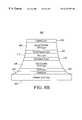
- FIG. 5depicts a bottom spin valve 200 accordance with the present invention.
- the bottom spin valve 200is formed using the method 100 in which IrMn, PtMn, PtPdMn, NiMn, RhMn, or CrPtMn is used in step 104 .
- the bottom spin valve 200is grown on a substrate 202 and includes an underlayer 204 , a seed layer 206 , an AFM layer 208 , a pinned layer 210 , a spacer layer 212 , a free layer 214 , and a capping layer 216 .
- the underlayer 204 and capping layer 216are preferably Ta.
- the substrateis preferably the first gap 3 of the MR head 1 .
- the pinned layer 210 and the free layer 214are magnetic and preferably made of a material such as Ni, Fe, Co, or alloys thereof
- the spacer layer 212is nonmagnetic and preferably Cu, Ag, or Au.
- the AFM layer 208is preferably PtMn, IrMn, PtPdMn, NiMn, RhMn, or CrPtMn.
- the seed layermay include NiFeX, Cu, or a bilayer of NiFe and Cu. In a preferred embodiment, X is Cr. Also in a preferred embodiment, the seed layer includes between twenty and fifty percent Cr and is on the order of thirty to forty Angstroms thick. Of this range, approximately twenty-five percent Cr is desired. If the seed layer 206 is NiFe alone, approximately fifteen to twenty Angstroms is desired. If the seed layer 206 is Cu, then approximately twenty Angstroms is desired.
- FIG. 6depicts a flow chart of a method 300 for providing a bottom spin valve having a synthetic antiferromagnet in accordance with the present invention.
- the bottom spin valvemay be used in a MR read head 1 depicted in FIG. 1.
- a seed layer having a preferred texture for the antiferromagnet that will be usedis provided in step 302 .
- the seed layer in step 302could be provided on a substrate or on an underlayer, such as a Ta underlayer.
- the seed layerhas several characteristics.
- the seed layerhas a texture appropriate for the desired synthetic antiferromagnet.
- the desired synthetic antiferromagnetincludes a layer IrMn, a layer of PtMn, a layer of PtPdMn, a layer of NiMn, a layer of RhMn, or a layer of CrPtMn.
- the seed layerincludes at least NiFe or Cu.
- the seed layeralso should have a relatively high resistivity. A seed layer having lower resistivity will shunt current away from the spin valve, reducing the magnetoresistance.
- NiFeXfulfills all these criteria.
- NiFeXis preferred for the seed layer provided in step 302 .
- the Xcan indicate a material in the Cr family, such as chromium, niobium, or rhodium.
- the Xcan also indicate absence of any material (NiFe alone).
- a synthetic AFM layeris then grown on the seed layer, via step 304 .
- the synthetic AFM layer formed in step 304includes a layer of PtMn and two layers of CoFe. The CoFe layers are separated by a Ru layer.
- the synthetic AFM layer formed in step 304includes a layer of IrMn and two layers of CoFe.
- the synthetic AFM layer formed in step 304could include a layer of RhMn, NiMn, CrPtMn or PtPdMn and two layers of CoFe. The CoFe layers are separated by a Ru layer.
- the CoFe and Ru layerswould each have the appropriate thickness to achieve strong antiferromagnetic coupling between the two CoFe layers and high magnetoresistance ( ⁇ R/R).
- a spacer layer and a free layerare then provided, via steps 306 and 308 , respectively.
- FIG. 7depicts the bottom spin valve 400 in which a synthetic antiferromagnet replaces the AFM layer 208 and the pinned layer 210 .
- the bottom spin valve 400is grown on a substrate 402 and includes an underlayer 404 , a seed layer 406 , a synthetic AFM layer 408 , a spacer layer 410 , a free layer 412 , and a capping layer 414 .
- the substrateis preferably the first gap 3 of the MR head 1 depicted in FIG. 1 .
- the underlayer 404 and capping layer 414are preferably Ta.
- the synthetic AFM layer 408is preferably includes a layers PtMn, IrMn, RhMn, NiMn, CrPtMn, or PtPdMn followed by two layers of CoFe separated by a layer of Ru.
- the seed layermay be NiFeX, Cu, or a bilayer of NiFe and Cu.
- Xis Cr.
- the seed layerincludes between twenty and fifty atomic percent Cr and is on the order of thirty to forty Angstroms thick. Of this range, approximately twenty-five percent Cr is desired. If the seed layer 206 is NiFe alone, approximately fifteen to twenty Angstroms is desired. If the seed layer 206 is Cu, then approximately twenty Angstroms is desired.
- the seed layer 206 or 406facilitates appropriate growth of the AFM layer 208 or the synthetic AFM layer 408 , respectively.
- NiFeX or Cuaids in growing the AFM layer 208 or the synthetic AFM layer 408 having the desired fcc (b 111 ) structure.
- the seed layer 206 or 406facilitates the growth of the AFM layer 208 or the synthetic AFM layer 408 , respectively. Consequently, the exchange coupling, measured by the exchange field, is increased. The magnetoresistance is also increased above that of the conventional bottom spin valve 50 not using a seed layer 206 or 406 .
- Table 1summarizes the results for bottom spin valves. Most of the bottom spin valves of Table 1 include a Ta underlayer that is thirty Angstroms thick, an AFM layer and a pinned layer or a synthetic AFM layer, a Cu spacer layer of twenty-five Angstroms, a free layer including ten Angstroms of CoFe and fifty Angstroms of NiFe, and a Ta capping layer of thirty Angstroms.
- the first bottom spin valve listedwhich has no seed layer, has a free layer that is different form the remaining bottom spin valves.
- the free layer for the first bottom spin valveincludes fifty Angstroms of NiFe and twenty Angstroms of CoFe. Consequently, the first bottom spin valve has a lower resistivity.
- the bottom spin valves 400 having a seed layer in accordance with the present inventionhave improved magnetoresistance while using PtMn and IrMn in the AFM layer 208 or the synthetic AFM layer 408 .
- NiO and CoOneed not be used in the bottom spin valve 400 .
- the method and systemcan be used to provide a dual spin valve.
- FIGS. 8A and 8Bdepict dual spin valves 500 and 800 , respectively, in accordance with the present invention.
- the dual spin valve 500includes an underlayer 204 ′, a seed layer 206 ′, a first AFM layer 208 ′, a first pinned layer 210 ′, a first spacer layer 212 ′, and a free layer 214 ′ that are analogous to the underlayer 204 , the seed layer 206 , the AFM layer 208 , the pinned layer 210 , the spacer layer 212 , and the free layer 214 of the bottom spin valve 200 .
- the dual spin valve 500also includes a second spacer layer 502 , a second pinned layer 504 , a second AFM layer 506 , and a capping layer 508 .
- the capping layer 508is analogous to the capping layer 216 or 414 .
- the second spacer layer 502 , the second pinned layer 504 , and the second AFM layer 506may be made of those materials used for the first spacer layer 212 ′, the first pinned layer 210 ′, and the first AFM layer 208 ′.
- the dual spin valve 600includes an underlayer 404 ′, a seed layer 406 ′, a first synthetic AFM layer 408 ′, a first spacer layer 410 ′, and a free layer 412 ′ that are analogous to the underlayer 404 , the seed layer 406 , synthetic the AFM layer 408 , the spacer layer 410 , and the free layer 412 of the bottom spin valve 400 .
- the dual spin valve 600also includes a second spacer layer 602 , a second synthetic AFM layer 604 , and a capping layer 606 .
- the capping layer 606is analogous to the capping layer 216 or 414 .
- the second spacer layer 602 and the second synthetic AFM layer 604may be made of those materials used for the first spacer layer 410 ′ and the first synthetic AFM layer 408 ′.
- a dual spin valvenot depicted in Table 1, was also fabricated and characterized.
- the dual spin valvewas fabricated without an underlayer and using thirty Angstroms of NiFeCr as a seed layer.
- the dual spin valvehad a magnetoresistance of fourteen percent, an exchange field of approximately 3200 Oe, and a resistivity of 8.89 ⁇ /sq.
- a method and systemhas been disclosed for providing a bottom spin valve using an antiferromagnet other than NiO or NiCoO and which has improved magnetoresistance.
- the method and systemcould also be used to provide a dual spin valve, which includes a bottom spin valve and a top spin valve.
- the free layer of the bottom spin valveis also the free layer of the top spin valve.
Landscapes
- Engineering & Computer Science (AREA)
- Chemical & Material Sciences (AREA)
- Crystallography & Structural Chemistry (AREA)
- Nanotechnology (AREA)
- Power Engineering (AREA)
- Manufacturing & Machinery (AREA)
- Physics & Mathematics (AREA)
- Mathematical Physics (AREA)
- Theoretical Computer Science (AREA)
- Hall/Mr Elements (AREA)
Abstract
Description
| TABLE 1 | ||||||
| Seed Layer | AFM/ | Exchange | Coercivity | Sheet | ||
| Seed Layer | Thickness | Synthetic | ΔR/R | Field | Of Pinned | Resistance |
| Composition | (Angstroms) | AFM | (percent) | (Oe) | Layer (Oe) | (Ω/sq) |
| None | N/A | PtMn | 5.35 | 449 | 598 | 14.87 |
| None | 15 | PtMn | 6.33 | 838 | 703 | 15.56 |
| Cu | 15 | PtMn | 5.92 | 886 | 641 | 16.1 |
| NiFe/Cu | 15/10 | 6 | 630 | 654 | 14.14 | |
| NiFe | 15 | Synthetic | 7.9 | 3390 | N/A | 13.4 |
| PtMn | ||||||
| NiFeCr | 30 | Synthetic | 9.42 | 3720 | N/A | 12.77 |
| PtMn | ||||||
| NiFeCr | 30 | Synthetic | 10.19 | Approx. | NIA | 14.9 |
| IrMn | 4500 | |||||
Claims (14)
Priority Applications (1)
| Application Number | Priority Date | Filing Date | Title |
|---|---|---|---|
| US09/221,799US6222707B1 (en) | 1998-12-28 | 1998-12-28 | Bottom or dual spin valve having a seed layer that results in an improved antiferromagnetic layer |
Applications Claiming Priority (1)
| Application Number | Priority Date | Filing Date | Title |
|---|---|---|---|
| US09/221,799US6222707B1 (en) | 1998-12-28 | 1998-12-28 | Bottom or dual spin valve having a seed layer that results in an improved antiferromagnetic layer |
Publications (1)
| Publication Number | Publication Date |
|---|---|
| US6222707B1true US6222707B1 (en) | 2001-04-24 |
Family
ID=22829440
Family Applications (1)
| Application Number | Title | Priority Date | Filing Date |
|---|---|---|---|
| US09/221,799Expired - LifetimeUS6222707B1 (en) | 1998-12-28 | 1998-12-28 | Bottom or dual spin valve having a seed layer that results in an improved antiferromagnetic layer |
Country Status (1)
| Country | Link |
|---|---|
| US (1) | US6222707B1 (en) |
Cited By (197)
| Publication number | Priority date | Publication date | Assignee | Title |
|---|---|---|---|---|
| US6317299B1 (en)* | 2000-02-17 | 2001-11-13 | International Business Machines Corporation | Seed layer for improving pinning field spin valve sensor |
| US6381105B1 (en)* | 1999-10-22 | 2002-04-30 | Read-Rite Corporation | Hybrid dual spin valve sensor and method for making same |
| US20020085320A1 (en)* | 2001-01-04 | 2002-07-04 | International Business Machines Corporation | AP-pinned spin valve design using very thin Pt-Mn AFM layer |
| US6433972B1 (en)* | 1999-04-28 | 2002-08-13 | Seagate Technology Llc | Giant magnetoresistive sensor with pinning layer |
| US6437950B1 (en)* | 2000-10-12 | 2002-08-20 | International Business Machines Corporation | Top spin valve sensor that has an iridium manganese (IrMn) pinning layer and an iridium manganese oxide (IrMnO) seed layer |
| US6496337B1 (en)* | 2000-03-20 | 2002-12-17 | Headway Technologies, Inc. | Copper alloy GMR recording head |
| US20020191356A1 (en)* | 2001-02-20 | 2002-12-19 | Alps Electric Co., Ltd. | Exchange coupled film having improved current-carrying reliability and improved rate of change in resistance and magnetic sensing element using same |
| US6498707B1 (en)* | 1999-04-20 | 2002-12-24 | Seagate Technology, Llc | Giant magnetoresistive sensor with a CrMnPt pinning layer and a NiFeCr seed layer |
| US20030002228A1 (en)* | 2001-06-28 | 2003-01-02 | Shigekazu Suwabe | Magnetic head |
| US6507457B2 (en)* | 2000-08-15 | 2003-01-14 | Qing He | Magnetic head |
| US6517896B1 (en)* | 2000-08-07 | 2003-02-11 | Headway Technologies, Inc. | Spin filter bottom spin valve head with continuous spacer exchange bias |
| US6535363B1 (en)* | 1999-01-13 | 2003-03-18 | Read-Rite Smi Corporation | Magnetic resistance effect type thin-film magnetic head and method for manufacturing the same |
| US20030053269A1 (en)* | 2001-09-14 | 2003-03-20 | Alps Electric Co., Ltd. | CPP magnetic sensing element and method for making the same |
| US6581272B1 (en) | 2002-01-04 | 2003-06-24 | Headway Technologies, Inc. | Method for forming a bottom spin valve magnetoresistive sensor element |
| US20030156362A1 (en)* | 2002-02-20 | 2003-08-21 | Gill Hardayal Singh | Magnetoresistance sensor having an antiferromagnetic pinning layer with both surfaces pinning ferromagnetic bias layers |
| US20030156361A1 (en)* | 2002-02-15 | 2003-08-21 | Min Li | Synthetic pattern exchange cofiguration for side reading reduction |
| US20030179517A1 (en)* | 2002-03-22 | 2003-09-25 | Headway Technologies, Inc. | Transverse or longitudinal patterned synthetic exchange biasing for stabilizing GMR sensors |
| US20030179514A1 (en)* | 2002-03-21 | 2003-09-25 | International Business Machines Corporation | Current perpendicular to the planes (CPP) spin valve sensor with in-stack biased free layer and self-pinned antiparallel (AP) pinned layer structure |
| US6650512B1 (en)* | 2000-03-21 | 2003-11-18 | International Business Machines Corporation | GMR coefficient enhancement of a spin valve structure |
| US20030231436A1 (en)* | 2002-06-13 | 2003-12-18 | Alps Electric Co., Ltd. | GMR magnetic sensing element having an antiferromagnetic layer extending beyond the track width and method for making the same |
| US20040047084A1 (en)* | 2002-09-10 | 2004-03-11 | Headway Technologies, Inc. | Novel spin-valve GMR with patterned synthetic exchange bias |
| US6710985B2 (en)* | 2000-06-14 | 2004-03-23 | Fujitsu Limited | Magnetoresistive film, magnetoresistive head, and information regeneration apparatus |
| US20040105193A1 (en)* | 2002-12-03 | 2004-06-03 | Headway Technologies, Inc. | Novel seed layers for fabricating spin valve heads for ultra-high density recordings |
| US6751072B2 (en) | 2002-03-21 | 2004-06-15 | Hitachi Global Storage Technologies Netherlands B.V. | High magnetoresistance spin valve sensor with self-pinned antiparallel (AP) pinned layer structure |
| US6771472B1 (en) | 2001-12-07 | 2004-08-03 | Seagate Technology Llc | Structure to achieve thermally stable high sensitivity and linear range in bridge GMR sensor using SAF magnetic alignments |
| US6770382B1 (en)* | 1999-11-22 | 2004-08-03 | Headway Technologies, Inc. | GMR configuration with enhanced spin filtering |
| US6773515B2 (en) | 2002-01-16 | 2004-08-10 | Headway Technologies, Inc. | FeTa nano-oxide layer as a capping layer for enhancement of giant magnetoresistance in bottom spin valve structures |
| US6775111B2 (en)* | 1999-10-28 | 2004-08-10 | International Business Machines Corporation | Trilayer seed layer structure for spin valve sensor |
| US6779248B2 (en) | 2002-03-07 | 2004-08-24 | Headway Technologies, Inc. | Method of manufacturing a lead overlay bottom spin valve with improved side reading |
| US6785102B2 (en) | 2002-04-18 | 2004-08-31 | Hitachi Global Storage Technologies Netherlands B.V. | Spin valve sensor with dual self-pinned AP pinned layer structures |
| US20040169958A1 (en)* | 2003-02-27 | 2004-09-02 | Krounbi Mohamad T. | Thin film recording head with a buried coil providing a shortened yoke and improved dimension control |
| US6807033B2 (en) | 2002-01-23 | 2004-10-19 | Carnegie Mellon University | Magnetic sensor with reduced wing region magnetic sensitivity |
| US20040252418A1 (en)* | 2003-06-12 | 2004-12-16 | Headway Technologies, Inc. | Bottom spin valve with laminated CoFe free layer for ultra-high density recording |
| US20050024793A1 (en)* | 2003-07-29 | 2005-02-03 | Alps Electric Co., Ltd. | Exchange-coupled film, method for making exchange-coupled film, and magnetic sensing element including exchange-coupled film |
| US6856493B2 (en) | 2002-03-21 | 2005-02-15 | International Business Machines Corporation | Spin valve sensor with in-stack biased free layer and antiparallel (AP) pinned layer pinned without a pinning layer |
| US20050047029A1 (en)* | 2003-09-03 | 2005-03-03 | Fujitsu Limited | Magnetoresistance effect film, magnetoresistance effect head and solid state memory |
| US6865062B2 (en) | 2002-03-21 | 2005-03-08 | International Business Machines Corporation | Spin valve sensor with exchange biased free layer and antiparallel (AP) pinned layer pinned without a pinning layer |
| US20050063105A1 (en)* | 2003-09-24 | 2005-03-24 | Hitachi Global Storage Technologies | GMR enhancing seedlayer for self pinned spin valves |
| US6873500B2 (en) | 2001-07-19 | 2005-03-29 | Alps Electric Co., Ltd. | Exchange coupling film capable of improving playback characteristics |
| US20050111143A1 (en)* | 2003-11-20 | 2005-05-26 | Headway Technologies, Inc. | Self-alignment scheme for enhancement of CPP-GMR |
| US20050111148A1 (en)* | 2003-11-20 | 2005-05-26 | Headway Technologies, Inc. | Method of increasing CPP GMR in a spin valve structure |
| US20050146912A1 (en)* | 2003-12-29 | 2005-07-07 | Deak James G. | Magnetic memory having synthetic antiferromagnetic pinned layer |
| US6954342B2 (en)* | 2001-04-30 | 2005-10-11 | Hitachi Global Storage Technologies Netherlands B.V. | Underlayer for high amplitude spin valve sensors |
| US20060002038A1 (en)* | 2004-07-01 | 2006-01-05 | Hitachi Global Storage Technologies | Pinning structure with trilayer pinned layer |
| US20060018057A1 (en)* | 2004-07-26 | 2006-01-26 | Yiming Huai | Magnetic tunnel junction having diffusion stop layer |
| US20060061915A1 (en)* | 2004-09-23 | 2006-03-23 | Headway Technologies, Inc. | CoFe insertion for exchange bias and sensor improvement |
| US20060092563A1 (en)* | 2004-10-29 | 2006-05-04 | Quang Le | Magnetic head with common seed layer for coil and pedestal |
| US20060168797A1 (en)* | 2005-01-31 | 2006-08-03 | Jinshan Li | Method of fabricating magnetic sensors with pinned layers with zero net magnetic moment |
| US20060193089A1 (en)* | 2005-02-28 | 2006-08-31 | Jinshan Li | GMR sensors with strongly pinning and pinned layers |
| US20070019342A1 (en)* | 2005-07-22 | 2007-01-25 | Hitachi Global Storage Technologies | Magnetoresistive sensor having an in stack bias structure with NiFeCr spacer layer for improved bias layer pinning |
| US20070063237A1 (en)* | 2005-09-20 | 2007-03-22 | Yiming Huai | Magnetic device having multilayered free ferromagnetic layer |
| US7196880B1 (en) | 1999-07-19 | 2007-03-27 | Western Digital (Fremont), Inc. | Spin valve sensor having a nonmagnetic enhancement layer adjacent an ultra thin free layer |
| US7224601B2 (en) | 2005-08-25 | 2007-05-29 | Grandis Inc. | Oscillating-field assisted spin torque switching of a magnetic tunnel junction memory element |
| US20070146928A1 (en)* | 2005-12-23 | 2007-06-28 | Headway Technologies, Inc. | Ultra thin seed layer for CPP or TMR structure |
| US20070171694A1 (en)* | 2005-12-23 | 2007-07-26 | Yiming Huai | Current-switched spin-transfer magnetic devices with reduced spin-transfer switching current density |
| US20070246787A1 (en)* | 2006-03-29 | 2007-10-25 | Lien-Chang Wang | On-plug magnetic tunnel junction devices based on spin torque transfer switching |
| US20080061388A1 (en)* | 2006-09-13 | 2008-03-13 | Zhitao Diao | Devices and circuits based on magnetic tunnel junctions utilizing a multilayer barrier |
| US20090050991A1 (en)* | 2007-08-22 | 2009-02-26 | Hide Nagai | Magnetic Element Having Low Saturation Magnetization |
| US20100067293A1 (en)* | 2008-09-12 | 2010-03-18 | David Chang-Cheng Yu | Programmable and Redundant Circuitry Based On Magnetic Tunnel Junction (MTJ) |
| US20100072524A1 (en)* | 2005-09-20 | 2010-03-25 | Yiming Huai | Magnetic Devices Having Oxide Antiferromagnetic Layer Next To Free Ferromagnetic Layer |
| US7777261B2 (en) | 2005-09-20 | 2010-08-17 | Grandis Inc. | Magnetic device having stabilized free ferromagnetic layer |
| US20100214835A1 (en)* | 2007-06-27 | 2010-08-26 | Yunfei Ding | Magnetic shielding in magnetic multilayer structures |
| US8493693B1 (en) | 2012-03-30 | 2013-07-23 | Western Digital (Fremont), Llc | Perpendicular magnetic recording transducer with AFM insertion layer |
| US8755152B1 (en) | 2008-09-24 | 2014-06-17 | Western Digital (Fremont), Llc | Method and system for providing an improved sensor stack for a recording head |
| US8830628B1 (en) | 2009-02-23 | 2014-09-09 | Western Digital (Fremont), Llc | Method and system for providing a perpendicular magnetic recording head |
| US8879207B1 (en) | 2011-12-20 | 2014-11-04 | Western Digital (Fremont), Llc | Method for providing a side shield for a magnetic recording transducer using an air bridge |
| US8883017B1 (en) | 2013-03-12 | 2014-11-11 | Western Digital (Fremont), Llc | Method and system for providing a read transducer having seamless interfaces |
| US8917581B1 (en) | 2013-12-18 | 2014-12-23 | Western Digital Technologies, Inc. | Self-anneal process for a near field transducer and chimney in a hard disk drive assembly |
| US8923102B1 (en) | 2013-07-16 | 2014-12-30 | Western Digital (Fremont), Llc | Optical grating coupling for interferometric waveguides in heat assisted magnetic recording heads |
| US8947985B1 (en) | 2013-07-16 | 2015-02-03 | Western Digital (Fremont), Llc | Heat assisted magnetic recording transducers having a recessed pole |
| US8953422B1 (en) | 2014-06-10 | 2015-02-10 | Western Digital (Fremont), Llc | Near field transducer using dielectric waveguide core with fine ridge feature |
| US8958272B1 (en) | 2014-06-10 | 2015-02-17 | Western Digital (Fremont), Llc | Interfering near field transducer for energy assisted magnetic recording |
| US8971160B1 (en) | 2013-12-19 | 2015-03-03 | Western Digital (Fremont), Llc | Near field transducer with high refractive index pin for heat assisted magnetic recording |
| US8970988B1 (en) | 2013-12-31 | 2015-03-03 | Western Digital (Fremont), Llc | Electric gaps and method for making electric gaps for multiple sensor arrays |
| US8976635B1 (en) | 2014-06-10 | 2015-03-10 | Western Digital (Fremont), Llc | Near field transducer driven by a transverse electric waveguide for energy assisted magnetic recording |
| US8980109B1 (en) | 2012-12-11 | 2015-03-17 | Western Digital (Fremont), Llc | Method for providing a magnetic recording transducer using a combined main pole and side shield CMP for a wraparound shield scheme |
| US8982508B1 (en) | 2011-10-31 | 2015-03-17 | Western Digital (Fremont), Llc | Method for providing a side shield for a magnetic recording transducer |
| US8984740B1 (en) | 2012-11-30 | 2015-03-24 | Western Digital (Fremont), Llc | Process for providing a magnetic recording transducer having a smooth magnetic seed layer |
| US8988825B1 (en) | 2014-02-28 | 2015-03-24 | Western Digital (Fremont, LLC | Method for fabricating a magnetic writer having half-side shields |
| US8988812B1 (en) | 2013-11-27 | 2015-03-24 | Western Digital (Fremont), Llc | Multi-sensor array configuration for a two-dimensional magnetic recording (TDMR) operation |
| US8993217B1 (en) | 2013-04-04 | 2015-03-31 | Western Digital (Fremont), Llc | Double exposure technique for high resolution disk imaging |
| US8995087B1 (en) | 2006-11-29 | 2015-03-31 | Western Digital (Fremont), Llc | Perpendicular magnetic recording write head having a wrap around shield |
| US8997832B1 (en) | 2010-11-23 | 2015-04-07 | Western Digital (Fremont), Llc | Method of fabricating micrometer scale components |
| US9001467B1 (en) | 2014-03-05 | 2015-04-07 | Western Digital (Fremont), Llc | Method for fabricating side shields in a magnetic writer |
| US9001628B1 (en) | 2013-12-16 | 2015-04-07 | Western Digital (Fremont), Llc | Assistant waveguides for evaluating main waveguide coupling efficiency and diode laser alignment tolerances for hard disk |
| US9007725B1 (en) | 2014-10-07 | 2015-04-14 | Western Digital (Fremont), Llc | Sensor with positive coupling between dual ferromagnetic free layer laminates |
| US9007719B1 (en) | 2013-10-23 | 2015-04-14 | Western Digital (Fremont), Llc | Systems and methods for using double mask techniques to achieve very small features |
| US9007879B1 (en) | 2014-06-10 | 2015-04-14 | Western Digital (Fremont), Llc | Interfering near field transducer having a wide metal bar feature for energy assisted magnetic recording |
| US9013836B1 (en) | 2013-04-02 | 2015-04-21 | Western Digital (Fremont), Llc | Method and system for providing an antiferromagnetically coupled return pole |
| US9042058B1 (en) | 2013-10-17 | 2015-05-26 | Western Digital Technologies, Inc. | Shield designed for middle shields in a multiple sensor array |
| US9042057B1 (en) | 2013-01-09 | 2015-05-26 | Western Digital (Fremont), Llc | Methods for providing magnetic storage elements with high magneto-resistance using Heusler alloys |
| US9042208B1 (en) | 2013-03-11 | 2015-05-26 | Western Digital Technologies, Inc. | Disk drive measuring fly height by applying a bias voltage to an electrically insulated write component of a head |
| US9042051B2 (en) | 2013-08-15 | 2015-05-26 | Western Digital (Fremont), Llc | Gradient write gap for perpendicular magnetic recording writer |
| US9042052B1 (en) | 2014-06-23 | 2015-05-26 | Western Digital (Fremont), Llc | Magnetic writer having a partially shunted coil |
| US9053735B1 (en) | 2014-06-20 | 2015-06-09 | Western Digital (Fremont), Llc | Method for fabricating a magnetic writer using a full-film metal planarization |
| US9064527B1 (en) | 2013-04-12 | 2015-06-23 | Western Digital (Fremont), Llc | High order tapered waveguide for use in a heat assisted magnetic recording head |
| US9064528B1 (en) | 2013-05-17 | 2015-06-23 | Western Digital Technologies, Inc. | Interferometric waveguide usable in shingled heat assisted magnetic recording in the absence of a near-field transducer |
| US9065043B1 (en) | 2012-06-29 | 2015-06-23 | Western Digital (Fremont), Llc | Tunnel magnetoresistance read head with narrow shield-to-shield spacing |
| US9064507B1 (en) | 2009-07-31 | 2015-06-23 | Western Digital (Fremont), Llc | Magnetic etch-stop layer for magnetoresistive read heads |
| US9070381B1 (en) | 2013-04-12 | 2015-06-30 | Western Digital (Fremont), Llc | Magnetic recording read transducer having a laminated free layer |
| US9082423B1 (en) | 2013-12-18 | 2015-07-14 | Western Digital (Fremont), Llc | Magnetic recording write transducer having an improved trailing surface profile |
| US9087534B1 (en) | 2011-12-20 | 2015-07-21 | Western Digital (Fremont), Llc | Method and system for providing a read transducer having soft and hard magnetic bias structures |
| US9087527B1 (en) | 2014-10-28 | 2015-07-21 | Western Digital (Fremont), Llc | Apparatus and method for middle shield connection in magnetic recording transducers |
| US9093639B2 (en) | 2012-02-21 | 2015-07-28 | Western Digital (Fremont), Llc | Methods for manufacturing a magnetoresistive structure utilizing heating and cooling |
| US9104107B1 (en) | 2013-04-03 | 2015-08-11 | Western Digital (Fremont), Llc | DUV photoresist process |
| US9111564B1 (en) | 2013-04-02 | 2015-08-18 | Western Digital (Fremont), Llc | Magnetic recording writer having a main pole with multiple flare angles |
| US9111558B1 (en) | 2014-03-14 | 2015-08-18 | Western Digital (Fremont), Llc | System and method of diffractive focusing of light in a waveguide |
| US9111550B1 (en) | 2014-12-04 | 2015-08-18 | Western Digital (Fremont), Llc | Write transducer having a magnetic buffer layer spaced between a side shield and a write pole by non-magnetic layers |
| US9123359B1 (en) | 2010-12-22 | 2015-09-01 | Western Digital (Fremont), Llc | Magnetic recording transducer with sputtered antiferromagnetic coupling trilayer between plated ferromagnetic shields and method of fabrication |
| US9123374B1 (en) | 2015-02-12 | 2015-09-01 | Western Digital (Fremont), Llc | Heat assisted magnetic recording writer having an integrated polarization rotation plate |
| US9123358B1 (en) | 2012-06-11 | 2015-09-01 | Western Digital (Fremont), Llc | Conformal high moment side shield seed layer for perpendicular magnetic recording writer |
| US9123362B1 (en) | 2011-03-22 | 2015-09-01 | Western Digital (Fremont), Llc | Methods for assembling an electrically assisted magnetic recording (EAMR) head |
| US9135937B1 (en) | 2014-05-09 | 2015-09-15 | Western Digital (Fremont), Llc | Current modulation on laser diode for energy assisted magnetic recording transducer |
| US9135930B1 (en) | 2014-03-06 | 2015-09-15 | Western Digital (Fremont), Llc | Method for fabricating a magnetic write pole using vacuum deposition |
| US9142233B1 (en) | 2014-02-28 | 2015-09-22 | Western Digital (Fremont), Llc | Heat assisted magnetic recording writer having a recessed pole |
| JP2015169530A (en)* | 2014-03-06 | 2015-09-28 | アルプス電気株式会社 | magnetic sensor |
| US9147404B1 (en) | 2015-03-31 | 2015-09-29 | Western Digital (Fremont), Llc | Method and system for providing a read transducer having a dual free layer |
| US9147408B1 (en) | 2013-12-19 | 2015-09-29 | Western Digital (Fremont), Llc | Heated AFM layer deposition and cooling process for TMR magnetic recording sensor with high pinning field |
| US9153255B1 (en) | 2014-03-05 | 2015-10-06 | Western Digital (Fremont), Llc | Method for fabricating a magnetic writer having an asymmetric gap and shields |
| US9183854B2 (en) | 2014-02-24 | 2015-11-10 | Western Digital (Fremont), Llc | Method to make interferometric taper waveguide for HAMR light delivery |
| US9190079B1 (en) | 2014-09-22 | 2015-11-17 | Western Digital (Fremont), Llc | Magnetic write pole having engineered radius of curvature and chisel angle profiles |
| US9190085B1 (en) | 2014-03-12 | 2015-11-17 | Western Digital (Fremont), Llc | Waveguide with reflective grating for localized energy intensity |
| US9194692B1 (en) | 2013-12-06 | 2015-11-24 | Western Digital (Fremont), Llc | Systems and methods for using white light interferometry to measure undercut of a bi-layer structure |
| US9202493B1 (en) | 2014-02-28 | 2015-12-01 | Western Digital (Fremont), Llc | Method of making an ultra-sharp tip mode converter for a HAMR head |
| US9202480B2 (en) | 2009-10-14 | 2015-12-01 | Western Digital (Fremont), LLC. | Double patterning hard mask for damascene perpendicular magnetic recording (PMR) writer |
| US9214172B2 (en) | 2013-10-23 | 2015-12-15 | Western Digital (Fremont), Llc | Method of manufacturing a magnetic read head |
| US9213322B1 (en) | 2012-08-16 | 2015-12-15 | Western Digital (Fremont), Llc | Methods for providing run to run process control using a dynamic tuner |
| US9214169B1 (en) | 2014-06-20 | 2015-12-15 | Western Digital (Fremont), Llc | Magnetic recording read transducer having a laminated free layer |
| US9214165B1 (en) | 2014-12-18 | 2015-12-15 | Western Digital (Fremont), Llc | Magnetic writer having a gradient in saturation magnetization of the shields |
| US9230565B1 (en) | 2014-06-24 | 2016-01-05 | Western Digital (Fremont), Llc | Magnetic shield for magnetic recording head |
| US9236560B1 (en) | 2014-12-08 | 2016-01-12 | Western Digital (Fremont), Llc | Spin transfer torque tunneling magnetoresistive device having a laminated free layer with perpendicular magnetic anisotropy |
| US9245562B1 (en) | 2015-03-30 | 2016-01-26 | Western Digital (Fremont), Llc | Magnetic recording writer with a composite main pole |
| US9245543B1 (en) | 2010-06-25 | 2016-01-26 | Western Digital (Fremont), Llc | Method for providing an energy assisted magnetic recording head having a laser integrally mounted to the slider |
| US9245545B1 (en) | 2013-04-12 | 2016-01-26 | Wester Digital (Fremont), Llc | Short yoke length coils for magnetic heads in disk drives |
| US9251813B1 (en) | 2009-04-19 | 2016-02-02 | Western Digital (Fremont), Llc | Method of making a magnetic recording head |
| US9263071B1 (en) | 2015-03-31 | 2016-02-16 | Western Digital (Fremont), Llc | Flat NFT for heat assisted magnetic recording |
| US9263067B1 (en) | 2013-05-29 | 2016-02-16 | Western Digital (Fremont), Llc | Process for making PMR writer with constant side wall angle |
| US9269382B1 (en) | 2012-06-29 | 2016-02-23 | Western Digital (Fremont), Llc | Method and system for providing a read transducer having improved pinning of the pinned layer at higher recording densities |
| US9275657B1 (en) | 2013-08-14 | 2016-03-01 | Western Digital (Fremont), Llc | Process for making PMR writer with non-conformal side gaps |
| US9280990B1 (en) | 2013-12-11 | 2016-03-08 | Western Digital (Fremont), Llc | Method for fabricating a magnetic writer using multiple etches |
| US9287494B1 (en) | 2013-06-28 | 2016-03-15 | Western Digital (Fremont), Llc | Magnetic tunnel junction (MTJ) with a magnesium oxide tunnel barrier |
| US9286919B1 (en) | 2014-12-17 | 2016-03-15 | Western Digital (Fremont), Llc | Magnetic writer having a dual side gap |
| US9305583B1 (en) | 2014-02-18 | 2016-04-05 | Western Digital (Fremont), Llc | Method for fabricating a magnetic writer using multiple etches of damascene materials |
| US9312064B1 (en) | 2015-03-02 | 2016-04-12 | Western Digital (Fremont), Llc | Method to fabricate a magnetic head including ion milling of read gap using dual layer hard mask |
| US9318130B1 (en) | 2013-07-02 | 2016-04-19 | Western Digital (Fremont), Llc | Method to fabricate tunneling magnetic recording heads with extended pinned layer |
| US9336814B1 (en) | 2013-03-12 | 2016-05-10 | Western Digital (Fremont), Llc | Inverse tapered waveguide for use in a heat assisted magnetic recording head |
| US9343086B1 (en) | 2013-09-11 | 2016-05-17 | Western Digital (Fremont), Llc | Magnetic recording write transducer having an improved sidewall angle profile |
| US9343098B1 (en) | 2013-08-23 | 2016-05-17 | Western Digital (Fremont), Llc | Method for providing a heat assisted magnetic recording transducer having protective pads |
| US9343087B1 (en) | 2014-12-21 | 2016-05-17 | Western Digital (Fremont), Llc | Method for fabricating a magnetic writer having half shields |
| US9341685B2 (en) | 2013-05-13 | 2016-05-17 | HGST Netherlands B.V. | Antiferromagnetic (AFM) grain growth controlled random telegraph noise (RTN) suppressed magnetic head |
| US9349394B1 (en) | 2013-10-18 | 2016-05-24 | Western Digital (Fremont), Llc | Method for fabricating a magnetic writer having a gradient side gap |
| US9349392B1 (en) | 2012-05-24 | 2016-05-24 | Western Digital (Fremont), Llc | Methods for improving adhesion on dielectric substrates |
| US9361913B1 (en) | 2013-06-03 | 2016-06-07 | Western Digital (Fremont), Llc | Recording read heads with a multi-layer AFM layer methods and apparatuses |
| US9361914B1 (en) | 2014-06-18 | 2016-06-07 | Western Digital (Fremont), Llc | Magnetic sensor with thin capping layer |
| US9368134B1 (en) | 2010-12-16 | 2016-06-14 | Western Digital (Fremont), Llc | Method and system for providing an antiferromagnetically coupled writer |
| US9384765B1 (en) | 2015-09-24 | 2016-07-05 | Western Digital (Fremont), Llc | Method and system for providing a HAMR writer having improved optical efficiency |
| US9384763B1 (en) | 2015-03-26 | 2016-07-05 | Western Digital (Fremont), Llc | Dual free layer magnetic reader having a rear bias structure including a soft bias layer |
| US9396743B1 (en) | 2014-02-28 | 2016-07-19 | Western Digital (Fremont), Llc | Systems and methods for controlling soft bias thickness for tunnel magnetoresistance readers |
| US9396742B1 (en) | 2012-11-30 | 2016-07-19 | Western Digital (Fremont), Llc | Magnetoresistive sensor for a magnetic storage system read head, and fabrication method thereof |
| US9406331B1 (en) | 2013-06-17 | 2016-08-02 | Western Digital (Fremont), Llc | Method for making ultra-narrow read sensor and read transducer device resulting therefrom |
| US9424866B1 (en) | 2015-09-24 | 2016-08-23 | Western Digital (Fremont), Llc | Heat assisted magnetic recording write apparatus having a dielectric gap |
| US9431031B1 (en) | 2015-03-24 | 2016-08-30 | Western Digital (Fremont), Llc | System and method for magnetic transducers having multiple sensors and AFC shields |
| US9431047B1 (en) | 2013-05-01 | 2016-08-30 | Western Digital (Fremont), Llc | Method for providing an improved AFM reader shield |
| US9431039B1 (en) | 2013-05-21 | 2016-08-30 | Western Digital (Fremont), Llc | Multiple sensor array usable in two-dimensional magnetic recording |
| US9431038B1 (en) | 2015-06-29 | 2016-08-30 | Western Digital (Fremont), Llc | Method for fabricating a magnetic write pole having an improved sidewall angle profile |
| US9431032B1 (en) | 2013-08-14 | 2016-08-30 | Western Digital (Fremont), Llc | Electrical connection arrangement for a multiple sensor array usable in two-dimensional magnetic recording |
| US9437251B1 (en) | 2014-12-22 | 2016-09-06 | Western Digital (Fremont), Llc | Apparatus and method having TDMR reader to reader shunts |
| US9443541B1 (en) | 2015-03-24 | 2016-09-13 | Western Digital (Fremont), Llc | Magnetic writer having a gradient in saturation magnetization of the shields and return pole |
| US9441938B1 (en) | 2013-10-08 | 2016-09-13 | Western Digital (Fremont), Llc | Test structures for measuring near field transducer disc length |
| US9449625B1 (en) | 2014-12-24 | 2016-09-20 | Western Digital (Fremont), Llc | Heat assisted magnetic recording head having a plurality of diffusion barrier layers |
| US9449621B1 (en) | 2015-03-26 | 2016-09-20 | Western Digital (Fremont), Llc | Dual free layer magnetic reader having a rear bias structure having a high aspect ratio |
| US9472216B1 (en) | 2015-09-23 | 2016-10-18 | Western Digital (Fremont), Llc | Differential dual free layer magnetic reader |
| US9484051B1 (en) | 2015-11-09 | 2016-11-01 | The Provost, Fellows, Foundation Scholars and the other members of Board, of the College of the Holy and Undivided Trinity of Queen Elizabeth near Dublin | Method and system for reducing undesirable reflections in a HAMR write apparatus |
| US9508363B1 (en) | 2014-06-17 | 2016-11-29 | Western Digital (Fremont), Llc | Method for fabricating a magnetic write pole having a leading edge bevel |
| US9508365B1 (en) | 2015-06-24 | 2016-11-29 | Western Digital (Fremont), LLC. | Magnetic reader having a crystal decoupling structure |
| US9508372B1 (en) | 2015-06-03 | 2016-11-29 | Western Digital (Fremont), Llc | Shingle magnetic writer having a low sidewall angle pole |
| US9530443B1 (en) | 2015-06-25 | 2016-12-27 | Western Digital (Fremont), Llc | Method for fabricating a magnetic recording device having a high aspect ratio structure |
| US9564150B1 (en) | 2015-11-24 | 2017-02-07 | Western Digital (Fremont), Llc | Magnetic read apparatus having an improved read sensor isolation circuit |
| US9595273B1 (en) | 2015-09-30 | 2017-03-14 | Western Digital (Fremont), Llc | Shingle magnetic writer having nonconformal shields |
| US9646639B2 (en) | 2015-06-26 | 2017-05-09 | Western Digital (Fremont), Llc | Heat assisted magnetic recording writer having integrated polarization rotation waveguides |
| US9666214B1 (en) | 2015-09-23 | 2017-05-30 | Western Digital (Fremont), Llc | Free layer magnetic reader that may have a reduced shield-to-shield spacing |
| US9721595B1 (en) | 2014-12-04 | 2017-08-01 | Western Digital (Fremont), Llc | Method for providing a storage device |
| US9741366B1 (en) | 2014-12-18 | 2017-08-22 | Western Digital (Fremont), Llc | Method for fabricating a magnetic writer having a gradient in saturation magnetization of the shields |
| US9740805B1 (en) | 2015-12-01 | 2017-08-22 | Western Digital (Fremont), Llc | Method and system for detecting hotspots for photolithographically-defined devices |
| US9754611B1 (en) | 2015-11-30 | 2017-09-05 | Western Digital (Fremont), Llc | Magnetic recording write apparatus having a stepped conformal trailing shield |
| US9767831B1 (en) | 2015-12-01 | 2017-09-19 | Western Digital (Fremont), Llc | Magnetic writer having convex trailing surface pole and conformal write gap |
| US9786301B1 (en) | 2014-12-02 | 2017-10-10 | Western Digital (Fremont), Llc | Apparatuses and methods for providing thin shields in a multiple sensor array |
| US9799351B1 (en) | 2015-11-30 | 2017-10-24 | Western Digital (Fremont), Llc | Short yoke length writer having assist coils |
| US9812155B1 (en) | 2015-11-23 | 2017-11-07 | Western Digital (Fremont), Llc | Method and system for fabricating high junction angle read sensors |
| US9842615B1 (en) | 2015-06-26 | 2017-12-12 | Western Digital (Fremont), Llc | Magnetic reader having a nonmagnetic insertion layer for the pinning layer |
| US9858951B1 (en) | 2015-12-01 | 2018-01-02 | Western Digital (Fremont), Llc | Method for providing a multilayer AFM layer in a read sensor |
| US9881638B1 (en) | 2014-12-17 | 2018-01-30 | Western Digital (Fremont), Llc | Method for providing a near-field transducer (NFT) for a heat assisted magnetic recording (HAMR) device |
| US9934811B1 (en) | 2014-03-07 | 2018-04-03 | Western Digital (Fremont), Llc | Methods for controlling stray fields of magnetic features using magneto-elastic anisotropy |
| US9953670B1 (en) | 2015-11-10 | 2018-04-24 | Western Digital (Fremont), Llc | Method and system for providing a HAMR writer including a multi-mode interference device |
| US10037770B1 (en) | 2015-11-12 | 2018-07-31 | Western Digital (Fremont), Llc | Method for providing a magnetic recording write apparatus having a seamless pole |
| US10074387B1 (en) | 2014-12-21 | 2018-09-11 | Western Digital (Fremont), Llc | Method and system for providing a read transducer having symmetric antiferromagnetically coupled shields |
| US11127420B1 (en) | 2018-09-06 | 2021-09-21 | Western Digital Technologies, Inc. | Seed layer for spin torque oscillator in microwave assisted magnetic recording device |
Citations (22)
| Publication number | Priority date | Publication date | Assignee | Title |
|---|---|---|---|---|
| US4900650A (en) | 1988-05-12 | 1990-02-13 | Digital Equipment Corporation | Method of producing a pole piece with improved magnetic domain structure |
| US4912584A (en) | 1988-03-09 | 1990-03-27 | Digital Equipment Corporation | Method for fabricating magnetic recording poles |
| US5111352A (en) | 1987-07-29 | 1992-05-05 | Digital Equipment Corporation | Three-pole magnetic head with reduced flux leakage |
| US5126971A (en) | 1989-12-22 | 1992-06-30 | Magnex Corporation | Thin film magnetic core memory and method of making same |
| US5311387A (en) | 1987-07-29 | 1994-05-10 | Digital Equipment Corporation | Three-pole magnetic recording head with high readback resolution |
| US5331728A (en) | 1989-11-07 | 1994-07-26 | International Business Machines Corporation | Method of fabricating magnetic thin film structures with edge closure layers |
| US5414580A (en) | 1994-05-13 | 1995-05-09 | International Business Machines Corporation | Magnetic storage system using thin film magnetic recording heads using phase-shifting mask |
| US5462637A (en) | 1993-07-22 | 1995-10-31 | International Business Machines Corporation | Process for fabrication of thin film magnetic heads |
| US5486968A (en) | 1993-11-10 | 1996-01-23 | International Business Machines Corporation | Method and apparatus for simultaneous write head planarization and lead routing |
| US5543989A (en) | 1993-01-15 | 1996-08-06 | International Business Machines Corporation | Magnetic storage system including a magnetoresistive read sensor with sendust shield utilizing an optimized sendust seed layer |
| US5559654A (en) | 1992-05-21 | 1996-09-24 | Das; Shyam C. | Narrow track thin film head for high track density recording |
| US5650897A (en) | 1992-07-21 | 1997-07-22 | Seagate Technology, Inc. | Thin film magnetic head including lightning arrester and process for making the same |
| US5659451A (en) | 1992-07-21 | 1997-08-19 | Seagate Technology, Inc. | Studless thin film magnetic head and process for making the same |
| US5703740A (en) | 1995-08-24 | 1997-12-30 | Velocidata, Inc. | Toroidal thin film head |
| US5751526A (en) | 1995-06-05 | 1998-05-12 | Mke-Quantum Components Colorado Llc | Flux enhanced write transducer and process for producing the same in conjunction with shared shields on magnetoresistive read heads |
| US5751528A (en) | 1996-04-15 | 1998-05-12 | Read-Rite Corporation | Multilayer exchange coupled magnetic poles with approximate zero magnetostriction |
| US5764056A (en)* | 1996-05-16 | 1998-06-09 | Seagate Technology, Inc. | Nickel-manganese as a pinning layer in spin valve/GMR magnetic sensors |
| US5766780A (en) | 1996-10-15 | 1998-06-16 | Seagate Technology, Inc. | Reversed order NIMN exchange biasing for dual magnetoresistive heads |
| JPH10331916A (en) | 1997-05-29 | 1998-12-15 | Mitsubishi Motors Corp | Damper device |
| US5883764A (en)* | 1997-10-03 | 1999-03-16 | International Business Machines Corporation | Magnetoresistive sensor having multi-layered refractory metal conductor leads |
| US5966012A (en)* | 1997-10-07 | 1999-10-12 | International Business Machines Corporation | Magnetic tunnel junction device with improved fixed and free ferromagnetic layers |
| US6074566A (en)* | 1997-09-16 | 2000-06-13 | International Business Machines Corporation | Thin film inductive write head with minimal organic insulation material and method for its manufacture |
- 1998
- 1998-12-28USUS09/221,799patent/US6222707B1/ennot_activeExpired - Lifetime
Patent Citations (25)
| Publication number | Priority date | Publication date | Assignee | Title |
|---|---|---|---|---|
| US5111352A (en) | 1987-07-29 | 1992-05-05 | Digital Equipment Corporation | Three-pole magnetic head with reduced flux leakage |
| US5311387A (en) | 1987-07-29 | 1994-05-10 | Digital Equipment Corporation | Three-pole magnetic recording head with high readback resolution |
| US4912584A (en) | 1988-03-09 | 1990-03-27 | Digital Equipment Corporation | Method for fabricating magnetic recording poles |
| US4900650A (en) | 1988-05-12 | 1990-02-13 | Digital Equipment Corporation | Method of producing a pole piece with improved magnetic domain structure |
| US5331728A (en) | 1989-11-07 | 1994-07-26 | International Business Machines Corporation | Method of fabricating magnetic thin film structures with edge closure layers |
| US5126971A (en) | 1989-12-22 | 1992-06-30 | Magnex Corporation | Thin film magnetic core memory and method of making same |
| US5559654A (en) | 1992-05-21 | 1996-09-24 | Das; Shyam C. | Narrow track thin film head for high track density recording |
| US5650897A (en) | 1992-07-21 | 1997-07-22 | Seagate Technology, Inc. | Thin film magnetic head including lightning arrester and process for making the same |
| US5659451A (en) | 1992-07-21 | 1997-08-19 | Seagate Technology, Inc. | Studless thin film magnetic head and process for making the same |
| US5686193A (en) | 1993-01-15 | 1997-11-11 | International Business Machines Corporation | Multilayered sendust films with a gas-doped sendust seed layer |
| US5543989A (en) | 1993-01-15 | 1996-08-06 | International Business Machines Corporation | Magnetic storage system including a magnetoresistive read sensor with sendust shield utilizing an optimized sendust seed layer |
| US5462637A (en) | 1993-07-22 | 1995-10-31 | International Business Machines Corporation | Process for fabrication of thin film magnetic heads |
| US5761013A (en) | 1993-11-10 | 1998-06-02 | International Business Machines Corporation | Apparatus for simultaneous write head planarization and lead routing |
| US5486968A (en) | 1993-11-10 | 1996-01-23 | International Business Machines Corporation | Method and apparatus for simultaneous write head planarization and lead routing |
| US5512394A (en) | 1994-05-13 | 1996-04-30 | International Business Machines Corporation | Method of coil fabrication for thin-film magnetic recording heads using phase-shifting masks |
| US5414580A (en) | 1994-05-13 | 1995-05-09 | International Business Machines Corporation | Magnetic storage system using thin film magnetic recording heads using phase-shifting mask |
| US5751526A (en) | 1995-06-05 | 1998-05-12 | Mke-Quantum Components Colorado Llc | Flux enhanced write transducer and process for producing the same in conjunction with shared shields on magnetoresistive read heads |
| US5703740A (en) | 1995-08-24 | 1997-12-30 | Velocidata, Inc. | Toroidal thin film head |
| US5751528A (en) | 1996-04-15 | 1998-05-12 | Read-Rite Corporation | Multilayer exchange coupled magnetic poles with approximate zero magnetostriction |
| US5764056A (en)* | 1996-05-16 | 1998-06-09 | Seagate Technology, Inc. | Nickel-manganese as a pinning layer in spin valve/GMR magnetic sensors |
| US5766780A (en) | 1996-10-15 | 1998-06-16 | Seagate Technology, Inc. | Reversed order NIMN exchange biasing for dual magnetoresistive heads |
| JPH10331916A (en) | 1997-05-29 | 1998-12-15 | Mitsubishi Motors Corp | Damper device |
| US6074566A (en)* | 1997-09-16 | 2000-06-13 | International Business Machines Corporation | Thin film inductive write head with minimal organic insulation material and method for its manufacture |
| US5883764A (en)* | 1997-10-03 | 1999-03-16 | International Business Machines Corporation | Magnetoresistive sensor having multi-layered refractory metal conductor leads |
| US5966012A (en)* | 1997-10-07 | 1999-10-12 | International Business Machines Corporation | Magnetic tunnel junction device with improved fixed and free ferromagnetic layers |
Cited By (285)
| Publication number | Priority date | Publication date | Assignee | Title |
|---|---|---|---|---|
| US6535363B1 (en)* | 1999-01-13 | 2003-03-18 | Read-Rite Smi Corporation | Magnetic resistance effect type thin-film magnetic head and method for manufacturing the same |
| US6498707B1 (en)* | 1999-04-20 | 2002-12-24 | Seagate Technology, Llc | Giant magnetoresistive sensor with a CrMnPt pinning layer and a NiFeCr seed layer |
| US6433972B1 (en)* | 1999-04-28 | 2002-08-13 | Seagate Technology Llc | Giant magnetoresistive sensor with pinning layer |
| US7196880B1 (en) | 1999-07-19 | 2007-03-27 | Western Digital (Fremont), Inc. | Spin valve sensor having a nonmagnetic enhancement layer adjacent an ultra thin free layer |
| US6381105B1 (en)* | 1999-10-22 | 2002-04-30 | Read-Rite Corporation | Hybrid dual spin valve sensor and method for making same |
| US6775111B2 (en)* | 1999-10-28 | 2004-08-10 | International Business Machines Corporation | Trilayer seed layer structure for spin valve sensor |
| US20040170867A1 (en)* | 1999-11-22 | 2004-09-02 | Headway Technologies, Inc. | GMR configuration with enhanced spin filtering |
| US6770382B1 (en)* | 1999-11-22 | 2004-08-03 | Headway Technologies, Inc. | GMR configuration with enhanced spin filtering |
| US6882509B2 (en)* | 1999-11-22 | 2005-04-19 | Headway Technologies, Inc. | GMR configuration with enhanced spin filtering |
| US6317299B1 (en)* | 2000-02-17 | 2001-11-13 | International Business Machines Corporation | Seed layer for improving pinning field spin valve sensor |
| US6496337B1 (en)* | 2000-03-20 | 2002-12-17 | Headway Technologies, Inc. | Copper alloy GMR recording head |
| US6650512B1 (en)* | 2000-03-21 | 2003-11-18 | International Business Machines Corporation | GMR coefficient enhancement of a spin valve structure |
| SG100636A1 (en)* | 2000-03-21 | 2003-12-26 | Ibm | Gmr coefficient enhancement of a spin valve structure |
| US6710985B2 (en)* | 2000-06-14 | 2004-03-23 | Fujitsu Limited | Magnetoresistive film, magnetoresistive head, and information regeneration apparatus |
| US6517896B1 (en)* | 2000-08-07 | 2003-02-11 | Headway Technologies, Inc. | Spin filter bottom spin valve head with continuous spacer exchange bias |
| US6507457B2 (en)* | 2000-08-15 | 2003-01-14 | Qing He | Magnetic head |
| US6437950B1 (en)* | 2000-10-12 | 2002-08-20 | International Business Machines Corporation | Top spin valve sensor that has an iridium manganese (IrMn) pinning layer and an iridium manganese oxide (IrMnO) seed layer |
| US6738237B2 (en)* | 2001-01-04 | 2004-05-18 | Hitachi Global Storage Technologies Netherlands B.V. | AP-pinned spin valve design using very thin Pt-Mn AFM layer |
| US20020085320A1 (en)* | 2001-01-04 | 2002-07-04 | International Business Machines Corporation | AP-pinned spin valve design using very thin Pt-Mn AFM layer |
| US7372672B2 (en) | 2001-02-05 | 2008-05-13 | Tdk Corporation | GMR magnetic sensing element having an antiferromagnetic layer extending beyond the track width and method for making the same |
| US20070252588A1 (en)* | 2001-02-05 | 2007-11-01 | Yoshihiro Nishiyama | GMR magnetic sensing element having an antiferromagnetic layer extending beyond the track width and method for making the same |
| US7050275B2 (en) | 2001-02-20 | 2006-05-23 | Alps Electric Co., Ltd. | Exchange coupled film having improved current-carrying reliability and improved rate of change in resistance and magnetic sensing element using same |
| US20020191356A1 (en)* | 2001-02-20 | 2002-12-19 | Alps Electric Co., Ltd. | Exchange coupled film having improved current-carrying reliability and improved rate of change in resistance and magnetic sensing element using same |
| US7092222B2 (en) | 2001-02-20 | 2006-08-15 | Alps Electric Co., Ltd. | Exchange coupled film having improved current-carrying reliability and improved rate of change in resistance and magnetic sensing element using same |
| US20050135021A1 (en)* | 2001-02-20 | 2005-06-23 | Alps Electric Co., Ltd. | Exchange coupled film having improved current-carrying reliability and improved rate of change in resistance and magnetic sensing element using same |
| US6954342B2 (en)* | 2001-04-30 | 2005-10-11 | Hitachi Global Storage Technologies Netherlands B.V. | Underlayer for high amplitude spin valve sensors |
| US6833981B2 (en)* | 2001-06-28 | 2004-12-21 | Hitachi, Ltd. | Spin valve magnetic head with three underlayers |
| US20030002228A1 (en)* | 2001-06-28 | 2003-01-02 | Shigekazu Suwabe | Magnetic head |
| US6873500B2 (en) | 2001-07-19 | 2005-03-29 | Alps Electric Co., Ltd. | Exchange coupling film capable of improving playback characteristics |
| US20030053269A1 (en)* | 2001-09-14 | 2003-03-20 | Alps Electric Co., Ltd. | CPP magnetic sensing element and method for making the same |
| US7248445B2 (en)* | 2001-09-14 | 2007-07-24 | Alps Electric Co., Ltd. | CPP magnetic sensing element and method for making the same |
| US6771472B1 (en) | 2001-12-07 | 2004-08-03 | Seagate Technology Llc | Structure to achieve thermally stable high sensitivity and linear range in bridge GMR sensor using SAF magnetic alignments |
| US6581272B1 (en) | 2002-01-04 | 2003-06-24 | Headway Technologies, Inc. | Method for forming a bottom spin valve magnetoresistive sensor element |
| US6909583B2 (en) | 2002-01-04 | 2005-06-21 | Headway Technologies, Inc. | FeTa nano-oxide layer in pinned layer for enhancement of giant magnetoresistance in bottom spin valve structures |
| US20030192168A1 (en)* | 2002-01-04 | 2003-10-16 | Headway Technologies, Inc. | FeTa nano-oxide layer in pinned layer for enhancement of giant magnetoresistance in bottom spin valve structures |
| US6773515B2 (en) | 2002-01-16 | 2004-08-10 | Headway Technologies, Inc. | FeTa nano-oxide layer as a capping layer for enhancement of giant magnetoresistance in bottom spin valve structures |
| US7262941B2 (en) | 2002-01-16 | 2007-08-28 | Headway Technologies, Inc. | FeTa nano-oxide layer as a capping layer for enhancement of giant magnetoresistance in bottom spin valve structures |
| US20040223266A1 (en)* | 2002-01-16 | 2004-11-11 | Headway Technologies, Inc. | FeTa nano-oxide layer as a capping layer for enhancement of giant magnetoresistance in bottom spin valve structures |
| US6807033B2 (en) | 2002-01-23 | 2004-10-19 | Carnegie Mellon University | Magnetic sensor with reduced wing region magnetic sensitivity |
| US20030156361A1 (en)* | 2002-02-15 | 2003-08-21 | Min Li | Synthetic pattern exchange cofiguration for side reading reduction |
| US20060061918A1 (en)* | 2002-02-15 | 2006-03-23 | Headway Technologies, Inc. | Synthetic pattern exchange configuration for side reading reduction |
| US7184248B2 (en) | 2002-02-15 | 2007-02-27 | Headway Technologies, Inc. | Synthetic pattern exchange configuration for side reading reduction |
| US7010848B2 (en) | 2002-02-15 | 2006-03-14 | Headway Technologies, Inc. | Synthetic pattern exchange configuration for side reading reduction |
| US20030156362A1 (en)* | 2002-02-20 | 2003-08-21 | Gill Hardayal Singh | Magnetoresistance sensor having an antiferromagnetic pinning layer with both surfaces pinning ferromagnetic bias layers |
| US6961225B2 (en)* | 2002-02-20 | 2005-11-01 | International Business Machines Corporation | Magnetoresistance sensor having an antiferromagnetic pinning layer with both surfaces pinning ferromagnetic bias layers |
| US20050007706A1 (en)* | 2002-03-07 | 2005-01-13 | Headway Technologies, Inc. | Lead overlay bottom spin valve with improved side reading |
| US7116531B2 (en) | 2002-03-07 | 2006-10-03 | Headway Technologies, Inc. | Lead overlay bottom spin valve with improved side reading |
| US6779248B2 (en) | 2002-03-07 | 2004-08-24 | Headway Technologies, Inc. | Method of manufacturing a lead overlay bottom spin valve with improved side reading |
| US6751072B2 (en) | 2002-03-21 | 2004-06-15 | Hitachi Global Storage Technologies Netherlands B.V. | High magnetoresistance spin valve sensor with self-pinned antiparallel (AP) pinned layer structure |
| US6856493B2 (en) | 2002-03-21 | 2005-02-15 | International Business Machines Corporation | Spin valve sensor with in-stack biased free layer and antiparallel (AP) pinned layer pinned without a pinning layer |
| US6865062B2 (en) | 2002-03-21 | 2005-03-08 | International Business Machines Corporation | Spin valve sensor with exchange biased free layer and antiparallel (AP) pinned layer pinned without a pinning layer |
| US20030179514A1 (en)* | 2002-03-21 | 2003-09-25 | International Business Machines Corporation | Current perpendicular to the planes (CPP) spin valve sensor with in-stack biased free layer and self-pinned antiparallel (AP) pinned layer structure |
| US6741432B2 (en)* | 2002-03-21 | 2004-05-25 | International Business Machines Corporation | Current perpendicular to the planes (CPP) spin valve sensor with in-stack biased free layer and self-pinned antiparallel (AP) pinned layer structure |
| US20050122638A1 (en)* | 2002-03-22 | 2005-06-09 | Headway Technologies, Inc. | Transverse or longitudinal patterned synthetic exchange biasing for stabilizing GMR sensors |
| US20050141149A1 (en)* | 2002-03-22 | 2005-06-30 | Headway Technologies, Inc. | Transverse or longitudinal patterned synthetic exchange biasing for stabilizing GMR sensors |
| US6857180B2 (en) | 2002-03-22 | 2005-02-22 | Headway Technologies, Inc. | Method for fabricating a patterned synthetic longitudinal exchange biased GMR sensor |
| US7134186B2 (en) | 2002-03-22 | 2006-11-14 | Headway Technologies, Inc. | Method for fabricating a patterned, synthetic transversely exchanged biased GMR sensor |
| US20050122637A1 (en)* | 2002-03-22 | 2005-06-09 | Headway Technologies, Inc. | Transverse or longitudinal patterned synthetic exchange biasing for stabilizing GMR sensors |
| US7152304B2 (en) | 2002-03-22 | 2006-12-26 | Headway Technologies, Inc. | Method for fabricating a patterned, synthetic transverse exchange biased GMR sensor |
| US20030179517A1 (en)* | 2002-03-22 | 2003-09-25 | Headway Technologies, Inc. | Transverse or longitudinal patterned synthetic exchange biasing for stabilizing GMR sensors |
| US7400475B2 (en) | 2002-03-22 | 2008-07-15 | Headway Technologies, Inc. | Patterned, synthetic longitudinally exchange biased GMR sensor |
| US6785102B2 (en) | 2002-04-18 | 2004-08-31 | Hitachi Global Storage Technologies Netherlands B.V. | Spin valve sensor with dual self-pinned AP pinned layer structures |
| US20030231436A1 (en)* | 2002-06-13 | 2003-12-18 | Alps Electric Co., Ltd. | GMR magnetic sensing element having an antiferromagnetic layer extending beyond the track width and method for making the same |
| US7050276B2 (en)* | 2002-06-13 | 2006-05-23 | Alps Electric Co., Ltd. | GMR magnetic sensing element having an antiferromagnetic layer extending beyond the track width and method for making the same |
| US20040047084A1 (en)* | 2002-09-10 | 2004-03-11 | Headway Technologies, Inc. | Novel spin-valve GMR with patterned synthetic exchange bias |
| US7123452B2 (en) | 2002-09-10 | 2006-10-17 | Headway Technologies, Inc. | Spin-valve GMR with patterned synthetic exchange bias |
| US7630176B2 (en) | 2002-12-03 | 2009-12-08 | Headway Technologies, Inc. | Seed layer for fabricating spin valve heads for ultra-high density recordings |
| US7234228B2 (en) | 2002-12-03 | 2007-06-26 | Headway Technologies, Inc. | Method of fabricating novel seed layers for fabricating spin valve heads |
| US20040105193A1 (en)* | 2002-12-03 | 2004-06-03 | Headway Technologies, Inc. | Novel seed layers for fabricating spin valve heads for ultra-high density recordings |
| US20070220740A1 (en)* | 2002-12-03 | 2007-09-27 | Headway Technologies, Inc. | Novel seed layer for fabricating spin valve heads for ultra-high density recordings |
| US20070223151A1 (en)* | 2002-12-03 | 2007-09-27 | Headway Technologies, Inc. | Novel seed layer for fabricating spin valve heads for ultra-high density recordings |
| US7564660B2 (en) | 2002-12-03 | 2009-07-21 | Headway Technologies, Inc. | Seed layer for fabricating spin valve heads for ultra-high density recordings |
| US7006327B2 (en) | 2003-02-27 | 2006-02-28 | Western Digital (Fremont), Inc. | Thin film recording head with a buried coil providing a shortened yoke and improved dimension control |
| US7386933B1 (en) | 2003-02-27 | 2008-06-17 | Western Digital (Fremont), Llc | Method of fabricating thin film write heads with a shortened yoke and improved dimension control |
| US20040169958A1 (en)* | 2003-02-27 | 2004-09-02 | Krounbi Mohamad T. | Thin film recording head with a buried coil providing a shortened yoke and improved dimension control |
| US20040252418A1 (en)* | 2003-06-12 | 2004-12-16 | Headway Technologies, Inc. | Bottom spin valve with laminated CoFe free layer for ultra-high density recording |
| US7542249B2 (en) | 2003-06-12 | 2009-06-02 | Headway Technologies, Inc. | Bottom spin valve with laminated CoFe free layer for ultra-high density recording |
| US7536772B2 (en) | 2003-06-12 | 2009-05-26 | Headway Technologies, Inc. | Method of manufacturing a bottom spin valve with a laminated CoFe free layer |
| US6993827B2 (en) | 2003-06-12 | 2006-02-07 | Headway Technologies, Inc. | Method of making a bottom spin valve |
| US20060056116A1 (en)* | 2003-06-12 | 2006-03-16 | Headway Technologies, Inc. | Bottom spin valve with laminated CoFe free layer for ultra-high density recording |
| US20050024793A1 (en)* | 2003-07-29 | 2005-02-03 | Alps Electric Co., Ltd. | Exchange-coupled film, method for making exchange-coupled film, and magnetic sensing element including exchange-coupled film |
| US20080068767A1 (en)* | 2003-07-29 | 2008-03-20 | Alps Electric Co., Ltd. | Exchange-coupled film, method for making exchange-coupled film, and magnetic sensing element including exchange-coupled film |
| US7365948B2 (en)* | 2003-07-29 | 2008-04-29 | Alps Electric Co., Ltd | Exchange-coupled film, method for making exchange-coupled film, and magnetic sensing element including exchange-coupled film |
| GB2404490B (en)* | 2003-07-29 | 2008-11-26 | Alps Electric Co Ltd | Exchange-coupled film and magnetic sensing element |
| US20050047029A1 (en)* | 2003-09-03 | 2005-03-03 | Fujitsu Limited | Magnetoresistance effect film, magnetoresistance effect head and solid state memory |
| US7154717B2 (en) | 2003-09-03 | 2006-12-26 | Fujitsu Limited | Magnetoresistance effect film, magnetoresistance effect head and solid state memory |
| EP1513167A3 (en)* | 2003-09-03 | 2005-09-07 | Fujitsu Limited | Magnetoresistance effect film, magnetoresistance effect head and solid state memory |
| US6961224B2 (en) | 2003-09-24 | 2005-11-01 | Hitachi Global Storage Technologies Netherlands, B.V. | GMR enhancing seed layer for self pinned spin valves |
| US20050063105A1 (en)* | 2003-09-24 | 2005-03-24 | Hitachi Global Storage Technologies | GMR enhancing seedlayer for self pinned spin valves |
| US7118680B2 (en)* | 2003-11-20 | 2006-10-10 | Headway Technologies, Inc. | Self-alignment scheme for enhancement of CPP-GMR |
| US20050111143A1 (en)* | 2003-11-20 | 2005-05-26 | Headway Technologies, Inc. | Self-alignment scheme for enhancement of CPP-GMR |
| US20050111148A1 (en)* | 2003-11-20 | 2005-05-26 | Headway Technologies, Inc. | Method of increasing CPP GMR in a spin valve structure |
| US7016168B2 (en)* | 2003-11-20 | 2006-03-21 | Headway Technologies, Inc. | Method of increasing CPP GMR in a spin valve structure |
| US20050146912A1 (en)* | 2003-12-29 | 2005-07-07 | Deak James G. | Magnetic memory having synthetic antiferromagnetic pinned layer |
| US20060226458A1 (en)* | 2003-12-29 | 2006-10-12 | Deak James G | Magnetic memory having synthetic antiferromagnetic pinned layer |
| US7072209B2 (en) | 2003-12-29 | 2006-07-04 | Micron Technology, Inc. | Magnetic memory having synthetic antiferromagnetic pinned layer |
| US7385842B2 (en) | 2003-12-29 | 2008-06-10 | Micron Technology, Inc. | Magnetic memory having synthetic antiferromagnetic pinned layer |
| US20060002038A1 (en)* | 2004-07-01 | 2006-01-05 | Hitachi Global Storage Technologies | Pinning structure with trilayer pinned layer |
| US7446982B2 (en) | 2004-07-01 | 2008-11-04 | Hitachi Global Storage Technologies Netherlands B.V. | Pinning structure with trilayer pinned layer |
| US20060018057A1 (en)* | 2004-07-26 | 2006-01-26 | Yiming Huai | Magnetic tunnel junction having diffusion stop layer |
| US7576956B2 (en) | 2004-07-26 | 2009-08-18 | Grandis Inc. | Magnetic tunnel junction having diffusion stop layer |
| US7564658B2 (en) | 2004-09-23 | 2009-07-21 | Headway Technologies, Inc. | CoFe insertion for exchange bias and sensor improvement |
| US20060061915A1 (en)* | 2004-09-23 | 2006-03-23 | Headway Technologies, Inc. | CoFe insertion for exchange bias and sensor improvement |
| US20060092563A1 (en)* | 2004-10-29 | 2006-05-04 | Quang Le | Magnetic head with common seed layer for coil and pedestal |
| US7228619B2 (en) | 2004-10-29 | 2007-06-12 | Hitachi Global Storage Technologies Netherlands B.V. | Method of manufacturing a magnetic head with common seed layer for coil and pedestal |
| US7367109B2 (en) | 2005-01-31 | 2008-05-06 | Hitachi Global Storage Technologies Netherlands B.V. | Method of fabricating magnetic sensors with pinned layers with zero net magnetic moment |
| US20060168797A1 (en)* | 2005-01-31 | 2006-08-03 | Jinshan Li | Method of fabricating magnetic sensors with pinned layers with zero net magnetic moment |
| US20060193089A1 (en)* | 2005-02-28 | 2006-08-31 | Jinshan Li | GMR sensors with strongly pinning and pinned layers |
| US7554775B2 (en) | 2005-02-28 | 2009-06-30 | Hitachi Global Storage Technologies Netherlands B.V. | GMR sensors with strongly pinning and pinned layers |
| US7397638B2 (en) | 2005-07-22 | 2008-07-08 | Hitachi Global Storage Technologies Netherlands B.V. | Magnetoresistive sensor having an in stack bias structure with NiFeCr spacer layer for improved bias layer pinning |
| US20070019342A1 (en)* | 2005-07-22 | 2007-01-25 | Hitachi Global Storage Technologies | Magnetoresistive sensor having an in stack bias structure with NiFeCr spacer layer for improved bias layer pinning |
| US7224601B2 (en) | 2005-08-25 | 2007-05-29 | Grandis Inc. | Oscillating-field assisted spin torque switching of a magnetic tunnel junction memory element |
| US20100072524A1 (en)* | 2005-09-20 | 2010-03-25 | Yiming Huai | Magnetic Devices Having Oxide Antiferromagnetic Layer Next To Free Ferromagnetic Layer |
| US7859034B2 (en) | 2005-09-20 | 2010-12-28 | Grandis Inc. | Magnetic devices having oxide antiferromagnetic layer next to free ferromagnetic layer |
| US20070063237A1 (en)* | 2005-09-20 | 2007-03-22 | Yiming Huai | Magnetic device having multilayered free ferromagnetic layer |
| US7973349B2 (en) | 2005-09-20 | 2011-07-05 | Grandis Inc. | Magnetic device having multilayered free ferromagnetic layer |
| US7777261B2 (en) | 2005-09-20 | 2010-08-17 | Grandis Inc. | Magnetic device having stabilized free ferromagnetic layer |
| US20070146928A1 (en)* | 2005-12-23 | 2007-06-28 | Headway Technologies, Inc. | Ultra thin seed layer for CPP or TMR structure |
| US7430135B2 (en) | 2005-12-23 | 2008-09-30 | Grandis Inc. | Current-switched spin-transfer magnetic devices with reduced spin-transfer switching current density |
| US20070171694A1 (en)* | 2005-12-23 | 2007-07-26 | Yiming Huai | Current-switched spin-transfer magnetic devices with reduced spin-transfer switching current density |
| US7646568B2 (en)* | 2005-12-23 | 2010-01-12 | Headway Technologies, Inc. | Ultra thin seed layer for CPP or TMR structure |
| US20070246787A1 (en)* | 2006-03-29 | 2007-10-25 | Lien-Chang Wang | On-plug magnetic tunnel junction devices based on spin torque transfer switching |
| US20080061388A1 (en)* | 2006-09-13 | 2008-03-13 | Zhitao Diao | Devices and circuits based on magnetic tunnel junctions utilizing a multilayer barrier |
| US7851840B2 (en) | 2006-09-13 | 2010-12-14 | Grandis Inc. | Devices and circuits based on magnetic tunnel junctions utilizing a multilayer barrier |
| US8995087B1 (en) | 2006-11-29 | 2015-03-31 | Western Digital (Fremont), Llc | Perpendicular magnetic recording write head having a wrap around shield |
| US8213221B2 (en) | 2007-06-27 | 2012-07-03 | Grandis, Inc. | Magnetic shielding in magnetic multilayer structures |
| US7957179B2 (en) | 2007-06-27 | 2011-06-07 | Grandis Inc. | Magnetic shielding in magnetic multilayer structures |
| US20110210410A1 (en)* | 2007-06-27 | 2011-09-01 | Grandis Inc. | Magnetic shielding in magnetic multilayer structures |
| US20100214835A1 (en)* | 2007-06-27 | 2010-08-26 | Yunfei Ding | Magnetic shielding in magnetic multilayer structures |
| US20090050991A1 (en)* | 2007-08-22 | 2009-02-26 | Hide Nagai | Magnetic Element Having Low Saturation Magnetization |
| US7982275B2 (en) | 2007-08-22 | 2011-07-19 | Grandis Inc. | Magnetic element having low saturation magnetization |
| US8476723B2 (en) | 2007-08-22 | 2013-07-02 | Grandis, Inc. | Magnetic element having low saturation magnetization |
| US7894248B2 (en) | 2008-09-12 | 2011-02-22 | Grandis Inc. | Programmable and redundant circuitry based on magnetic tunnel junction (MTJ) |
| US20100067293A1 (en)* | 2008-09-12 | 2010-03-18 | David Chang-Cheng Yu | Programmable and Redundant Circuitry Based On Magnetic Tunnel Junction (MTJ) |
| US8755152B1 (en) | 2008-09-24 | 2014-06-17 | Western Digital (Fremont), Llc | Method and system for providing an improved sensor stack for a recording head |
| US8830628B1 (en) | 2009-02-23 | 2014-09-09 | Western Digital (Fremont), Llc | Method and system for providing a perpendicular magnetic recording head |
| US9251813B1 (en) | 2009-04-19 | 2016-02-02 | Western Digital (Fremont), Llc | Method of making a magnetic recording head |
| US9064507B1 (en) | 2009-07-31 | 2015-06-23 | Western Digital (Fremont), Llc | Magnetic etch-stop layer for magnetoresistive read heads |
| US9202480B2 (en) | 2009-10-14 | 2015-12-01 | Western Digital (Fremont), LLC. | Double patterning hard mask for damascene perpendicular magnetic recording (PMR) writer |
| US9245543B1 (en) | 2010-06-25 | 2016-01-26 | Western Digital (Fremont), Llc | Method for providing an energy assisted magnetic recording head having a laser integrally mounted to the slider |
| US9159345B1 (en) | 2010-11-23 | 2015-10-13 | Western Digital (Fremont), Llc | Micrometer scale components |
| US9672847B2 (en) | 2010-11-23 | 2017-06-06 | Western Digital (Fremont), Llc | Micrometer scale components |
| US8997832B1 (en) | 2010-11-23 | 2015-04-07 | Western Digital (Fremont), Llc | Method of fabricating micrometer scale components |
| US9368134B1 (en) | 2010-12-16 | 2016-06-14 | Western Digital (Fremont), Llc | Method and system for providing an antiferromagnetically coupled writer |
| US9123359B1 (en) | 2010-12-22 | 2015-09-01 | Western Digital (Fremont), Llc | Magnetic recording transducer with sputtered antiferromagnetic coupling trilayer between plated ferromagnetic shields and method of fabrication |
| US9123362B1 (en) | 2011-03-22 | 2015-09-01 | Western Digital (Fremont), Llc | Methods for assembling an electrically assisted magnetic recording (EAMR) head |
| US8982508B1 (en) | 2011-10-31 | 2015-03-17 | Western Digital (Fremont), Llc | Method for providing a side shield for a magnetic recording transducer |
| US9087534B1 (en) | 2011-12-20 | 2015-07-21 | Western Digital (Fremont), Llc | Method and system for providing a read transducer having soft and hard magnetic bias structures |
| US8879207B1 (en) | 2011-12-20 | 2014-11-04 | Western Digital (Fremont), Llc | Method for providing a side shield for a magnetic recording transducer using an air bridge |
| US9093639B2 (en) | 2012-02-21 | 2015-07-28 | Western Digital (Fremont), Llc | Methods for manufacturing a magnetoresistive structure utilizing heating and cooling |
| US8493693B1 (en) | 2012-03-30 | 2013-07-23 | Western Digital (Fremont), Llc | Perpendicular magnetic recording transducer with AFM insertion layer |
| US9349392B1 (en) | 2012-05-24 | 2016-05-24 | Western Digital (Fremont), Llc | Methods for improving adhesion on dielectric substrates |
| US9940950B2 (en) | 2012-05-24 | 2018-04-10 | Western Digital (Fremont), Llc | Methods for improving adhesion on dielectric substrates |
| US9123358B1 (en) | 2012-06-11 | 2015-09-01 | Western Digital (Fremont), Llc | Conformal high moment side shield seed layer for perpendicular magnetic recording writer |
| US9412400B2 (en) | 2012-06-29 | 2016-08-09 | Western Digital (Fremont), Llc | Tunnel magnetoresistance read head with narrow shield-to-shield spacing |
| US9065043B1 (en) | 2012-06-29 | 2015-06-23 | Western Digital (Fremont), Llc | Tunnel magnetoresistance read head with narrow shield-to-shield spacing |
| US9269382B1 (en) | 2012-06-29 | 2016-02-23 | Western Digital (Fremont), Llc | Method and system for providing a read transducer having improved pinning of the pinned layer at higher recording densities |
| US9213322B1 (en) | 2012-08-16 | 2015-12-15 | Western Digital (Fremont), Llc | Methods for providing run to run process control using a dynamic tuner |
| US8984740B1 (en) | 2012-11-30 | 2015-03-24 | Western Digital (Fremont), Llc | Process for providing a magnetic recording transducer having a smooth magnetic seed layer |
| US9396742B1 (en) | 2012-11-30 | 2016-07-19 | Western Digital (Fremont), Llc | Magnetoresistive sensor for a magnetic storage system read head, and fabrication method thereof |
| US8980109B1 (en) | 2012-12-11 | 2015-03-17 | Western Digital (Fremont), Llc | Method for providing a magnetic recording transducer using a combined main pole and side shield CMP for a wraparound shield scheme |
| US9042057B1 (en) | 2013-01-09 | 2015-05-26 | Western Digital (Fremont), Llc | Methods for providing magnetic storage elements with high magneto-resistance using Heusler alloys |
| US9042208B1 (en) | 2013-03-11 | 2015-05-26 | Western Digital Technologies, Inc. | Disk drive measuring fly height by applying a bias voltage to an electrically insulated write component of a head |
| US8883017B1 (en) | 2013-03-12 | 2014-11-11 | Western Digital (Fremont), Llc | Method and system for providing a read transducer having seamless interfaces |
| US9336814B1 (en) | 2013-03-12 | 2016-05-10 | Western Digital (Fremont), Llc | Inverse tapered waveguide for use in a heat assisted magnetic recording head |
| US9013836B1 (en) | 2013-04-02 | 2015-04-21 | Western Digital (Fremont), Llc | Method and system for providing an antiferromagnetically coupled return pole |
| US9111564B1 (en) | 2013-04-02 | 2015-08-18 | Western Digital (Fremont), Llc | Magnetic recording writer having a main pole with multiple flare angles |
| US9104107B1 (en) | 2013-04-03 | 2015-08-11 | Western Digital (Fremont), Llc | DUV photoresist process |
| US8993217B1 (en) | 2013-04-04 | 2015-03-31 | Western Digital (Fremont), Llc | Double exposure technique for high resolution disk imaging |
| US9064527B1 (en) | 2013-04-12 | 2015-06-23 | Western Digital (Fremont), Llc | High order tapered waveguide for use in a heat assisted magnetic recording head |
| US9070381B1 (en) | 2013-04-12 | 2015-06-30 | Western Digital (Fremont), Llc | Magnetic recording read transducer having a laminated free layer |
| US9245545B1 (en) | 2013-04-12 | 2016-01-26 | Wester Digital (Fremont), Llc | Short yoke length coils for magnetic heads in disk drives |
| US9431047B1 (en) | 2013-05-01 | 2016-08-30 | Western Digital (Fremont), Llc | Method for providing an improved AFM reader shield |
| US9341685B2 (en) | 2013-05-13 | 2016-05-17 | HGST Netherlands B.V. | Antiferromagnetic (AFM) grain growth controlled random telegraph noise (RTN) suppressed magnetic head |
| US9064528B1 (en) | 2013-05-17 | 2015-06-23 | Western Digital Technologies, Inc. | Interferometric waveguide usable in shingled heat assisted magnetic recording in the absence of a near-field transducer |
| US9431039B1 (en) | 2013-05-21 | 2016-08-30 | Western Digital (Fremont), Llc | Multiple sensor array usable in two-dimensional magnetic recording |
| US9263067B1 (en) | 2013-05-29 | 2016-02-16 | Western Digital (Fremont), Llc | Process for making PMR writer with constant side wall angle |
| US9361913B1 (en) | 2013-06-03 | 2016-06-07 | Western Digital (Fremont), Llc | Recording read heads with a multi-layer AFM layer methods and apparatuses |
| US9406331B1 (en) | 2013-06-17 | 2016-08-02 | Western Digital (Fremont), Llc | Method for making ultra-narrow read sensor and read transducer device resulting therefrom |
| US9287494B1 (en) | 2013-06-28 | 2016-03-15 | Western Digital (Fremont), Llc | Magnetic tunnel junction (MTJ) with a magnesium oxide tunnel barrier |
| US9318130B1 (en) | 2013-07-02 | 2016-04-19 | Western Digital (Fremont), Llc | Method to fabricate tunneling magnetic recording heads with extended pinned layer |
| US8947985B1 (en) | 2013-07-16 | 2015-02-03 | Western Digital (Fremont), Llc | Heat assisted magnetic recording transducers having a recessed pole |
| US8923102B1 (en) | 2013-07-16 | 2014-12-30 | Western Digital (Fremont), Llc | Optical grating coupling for interferometric waveguides in heat assisted magnetic recording heads |
| US9275657B1 (en) | 2013-08-14 | 2016-03-01 | Western Digital (Fremont), Llc | Process for making PMR writer with non-conformal side gaps |
| US9431032B1 (en) | 2013-08-14 | 2016-08-30 | Western Digital (Fremont), Llc | Electrical connection arrangement for a multiple sensor array usable in two-dimensional magnetic recording |
| US9042051B2 (en) | 2013-08-15 | 2015-05-26 | Western Digital (Fremont), Llc | Gradient write gap for perpendicular magnetic recording writer |
| US9343098B1 (en) | 2013-08-23 | 2016-05-17 | Western Digital (Fremont), Llc | Method for providing a heat assisted magnetic recording transducer having protective pads |
| US9343086B1 (en) | 2013-09-11 | 2016-05-17 | Western Digital (Fremont), Llc | Magnetic recording write transducer having an improved sidewall angle profile |
| US9441938B1 (en) | 2013-10-08 | 2016-09-13 | Western Digital (Fremont), Llc | Test structures for measuring near field transducer disc length |
| US9042058B1 (en) | 2013-10-17 | 2015-05-26 | Western Digital Technologies, Inc. | Shield designed for middle shields in a multiple sensor array |
| US9349394B1 (en) | 2013-10-18 | 2016-05-24 | Western Digital (Fremont), Llc | Method for fabricating a magnetic writer having a gradient side gap |
| US9830936B2 (en) | 2013-10-23 | 2017-11-28 | Western Digital (Fremont), Llc | Magnetic read head with antiferromagentic layer |
| US9007719B1 (en) | 2013-10-23 | 2015-04-14 | Western Digital (Fremont), Llc | Systems and methods for using double mask techniques to achieve very small features |
| US9214172B2 (en) | 2013-10-23 | 2015-12-15 | Western Digital (Fremont), Llc | Method of manufacturing a magnetic read head |
| US8988812B1 (en) | 2013-11-27 | 2015-03-24 | Western Digital (Fremont), Llc | Multi-sensor array configuration for a two-dimensional magnetic recording (TDMR) operation |
| US9194692B1 (en) | 2013-12-06 | 2015-11-24 | Western Digital (Fremont), Llc | Systems and methods for using white light interferometry to measure undercut of a bi-layer structure |
| US9280990B1 (en) | 2013-12-11 | 2016-03-08 | Western Digital (Fremont), Llc | Method for fabricating a magnetic writer using multiple etches |
| US9001628B1 (en) | 2013-12-16 | 2015-04-07 | Western Digital (Fremont), Llc | Assistant waveguides for evaluating main waveguide coupling efficiency and diode laser alignment tolerances for hard disk |
| US9082423B1 (en) | 2013-12-18 | 2015-07-14 | Western Digital (Fremont), Llc | Magnetic recording write transducer having an improved trailing surface profile |
| US8917581B1 (en) | 2013-12-18 | 2014-12-23 | Western Digital Technologies, Inc. | Self-anneal process for a near field transducer and chimney in a hard disk drive assembly |
| US8971160B1 (en) | 2013-12-19 | 2015-03-03 | Western Digital (Fremont), Llc | Near field transducer with high refractive index pin for heat assisted magnetic recording |
| US9147408B1 (en) | 2013-12-19 | 2015-09-29 | Western Digital (Fremont), Llc | Heated AFM layer deposition and cooling process for TMR magnetic recording sensor with high pinning field |
| US8970988B1 (en) | 2013-12-31 | 2015-03-03 | Western Digital (Fremont), Llc | Electric gaps and method for making electric gaps for multiple sensor arrays |
| US9305583B1 (en) | 2014-02-18 | 2016-04-05 | Western Digital (Fremont), Llc | Method for fabricating a magnetic writer using multiple etches of damascene materials |
| US9183854B2 (en) | 2014-02-24 | 2015-11-10 | Western Digital (Fremont), Llc | Method to make interferometric taper waveguide for HAMR light delivery |
| US9142233B1 (en) | 2014-02-28 | 2015-09-22 | Western Digital (Fremont), Llc | Heat assisted magnetic recording writer having a recessed pole |
| US9396743B1 (en) | 2014-02-28 | 2016-07-19 | Western Digital (Fremont), Llc | Systems and methods for controlling soft bias thickness for tunnel magnetoresistance readers |
| US8988825B1 (en) | 2014-02-28 | 2015-03-24 | Western Digital (Fremont, LLC | Method for fabricating a magnetic writer having half-side shields |
| US9202493B1 (en) | 2014-02-28 | 2015-12-01 | Western Digital (Fremont), Llc | Method of making an ultra-sharp tip mode converter for a HAMR head |
| US9153255B1 (en) | 2014-03-05 | 2015-10-06 | Western Digital (Fremont), Llc | Method for fabricating a magnetic writer having an asymmetric gap and shields |
| US9349393B2 (en) | 2014-03-05 | 2016-05-24 | Western Digital (Fremont), Llc | Magnetic writer having an asymmetric gap and shields |
| US9001467B1 (en) | 2014-03-05 | 2015-04-07 | Western Digital (Fremont), Llc | Method for fabricating side shields in a magnetic writer |
| JP2015169530A (en)* | 2014-03-06 | 2015-09-28 | アルプス電気株式会社 | magnetic sensor |
| US9135930B1 (en) | 2014-03-06 | 2015-09-15 | Western Digital (Fremont), Llc | Method for fabricating a magnetic write pole using vacuum deposition |
| US9934811B1 (en) | 2014-03-07 | 2018-04-03 | Western Digital (Fremont), Llc | Methods for controlling stray fields of magnetic features using magneto-elastic anisotropy |
| US9495984B2 (en) | 2014-03-12 | 2016-11-15 | Western Digital (Fremont), Llc | Waveguide with reflective grating for localized energy intensity |
| US9190085B1 (en) | 2014-03-12 | 2015-11-17 | Western Digital (Fremont), Llc | Waveguide with reflective grating for localized energy intensity |
| US9111558B1 (en) | 2014-03-14 | 2015-08-18 | Western Digital (Fremont), Llc | System and method of diffractive focusing of light in a waveguide |
| US9135937B1 (en) | 2014-05-09 | 2015-09-15 | Western Digital (Fremont), Llc | Current modulation on laser diode for energy assisted magnetic recording transducer |
| US8976635B1 (en) | 2014-06-10 | 2015-03-10 | Western Digital (Fremont), Llc | Near field transducer driven by a transverse electric waveguide for energy assisted magnetic recording |
| US9311952B2 (en) | 2014-06-10 | 2016-04-12 | Western Digital (Fremont), Llc | Interfering near field transducer for energy assisted magnetic recording |
| US9159346B1 (en) | 2014-06-10 | 2015-10-13 | Western Digital (Fremont), Llc | Near field transducer using dielectric waveguide core with fine ridge feature |
| US8953422B1 (en) | 2014-06-10 | 2015-02-10 | Western Digital (Fremont), Llc | Near field transducer using dielectric waveguide core with fine ridge feature |
| US8958272B1 (en) | 2014-06-10 | 2015-02-17 | Western Digital (Fremont), Llc | Interfering near field transducer for energy assisted magnetic recording |
| US9007879B1 (en) | 2014-06-10 | 2015-04-14 | Western Digital (Fremont), Llc | Interfering near field transducer having a wide metal bar feature for energy assisted magnetic recording |
| US9508363B1 (en) | 2014-06-17 | 2016-11-29 | Western Digital (Fremont), Llc | Method for fabricating a magnetic write pole having a leading edge bevel |
| US9361914B1 (en) | 2014-06-18 | 2016-06-07 | Western Digital (Fremont), Llc | Magnetic sensor with thin capping layer |
| US9053735B1 (en) | 2014-06-20 | 2015-06-09 | Western Digital (Fremont), Llc | Method for fabricating a magnetic writer using a full-film metal planarization |
| US9214169B1 (en) | 2014-06-20 | 2015-12-15 | Western Digital (Fremont), Llc | Magnetic recording read transducer having a laminated free layer |
| US9042052B1 (en) | 2014-06-23 | 2015-05-26 | Western Digital (Fremont), Llc | Magnetic writer having a partially shunted coil |
| US9230565B1 (en) | 2014-06-24 | 2016-01-05 | Western Digital (Fremont), Llc | Magnetic shield for magnetic recording head |
| US9190079B1 (en) | 2014-09-22 | 2015-11-17 | Western Digital (Fremont), Llc | Magnetic write pole having engineered radius of curvature and chisel angle profiles |
| US9007725B1 (en) | 2014-10-07 | 2015-04-14 | Western Digital (Fremont), Llc | Sensor with positive coupling between dual ferromagnetic free layer laminates |
| US9087527B1 (en) | 2014-10-28 | 2015-07-21 | Western Digital (Fremont), Llc | Apparatus and method for middle shield connection in magnetic recording transducers |
| US9786301B1 (en) | 2014-12-02 | 2017-10-10 | Western Digital (Fremont), Llc | Apparatuses and methods for providing thin shields in a multiple sensor array |
| US9721595B1 (en) | 2014-12-04 | 2017-08-01 | Western Digital (Fremont), Llc | Method for providing a storage device |
| US9111550B1 (en) | 2014-12-04 | 2015-08-18 | Western Digital (Fremont), Llc | Write transducer having a magnetic buffer layer spaced between a side shield and a write pole by non-magnetic layers |
| US9236560B1 (en) | 2014-12-08 | 2016-01-12 | Western Digital (Fremont), Llc | Spin transfer torque tunneling magnetoresistive device having a laminated free layer with perpendicular magnetic anisotropy |
| US9705072B2 (en) | 2014-12-08 | 2017-07-11 | Western Digital (Fremont), Llc | Spin transfer torque tunneling magnetoresistive device having a laminated free layer with perpendicular magnetic anisotropy |
| US10553241B2 (en) | 2014-12-17 | 2020-02-04 | Western Digital Technologies, Inc. | Near-field transducer (NFT) for a heat assisted magnetic recording (HAMR) device |
| US9286919B1 (en) | 2014-12-17 | 2016-03-15 | Western Digital (Fremont), Llc | Magnetic writer having a dual side gap |
| US9881638B1 (en) | 2014-12-17 | 2018-01-30 | Western Digital (Fremont), Llc | Method for providing a near-field transducer (NFT) for a heat assisted magnetic recording (HAMR) device |
| US9741366B1 (en) | 2014-12-18 | 2017-08-22 | Western Digital (Fremont), Llc | Method for fabricating a magnetic writer having a gradient in saturation magnetization of the shields |
| US9214165B1 (en) | 2014-12-18 | 2015-12-15 | Western Digital (Fremont), Llc | Magnetic writer having a gradient in saturation magnetization of the shields |
| US10074387B1 (en) | 2014-12-21 | 2018-09-11 | Western Digital (Fremont), Llc | Method and system for providing a read transducer having symmetric antiferromagnetically coupled shields |
| US9343087B1 (en) | 2014-12-21 | 2016-05-17 | Western Digital (Fremont), Llc | Method for fabricating a magnetic writer having half shields |
| US9437251B1 (en) | 2014-12-22 | 2016-09-06 | Western Digital (Fremont), Llc | Apparatus and method having TDMR reader to reader shunts |
| US9449625B1 (en) | 2014-12-24 | 2016-09-20 | Western Digital (Fremont), Llc | Heat assisted magnetic recording head having a plurality of diffusion barrier layers |
| US9123374B1 (en) | 2015-02-12 | 2015-09-01 | Western Digital (Fremont), Llc | Heat assisted magnetic recording writer having an integrated polarization rotation plate |
| US9312064B1 (en) | 2015-03-02 | 2016-04-12 | Western Digital (Fremont), Llc | Method to fabricate a magnetic head including ion milling of read gap using dual layer hard mask |
| US9443541B1 (en) | 2015-03-24 | 2016-09-13 | Western Digital (Fremont), Llc | Magnetic writer having a gradient in saturation magnetization of the shields and return pole |
| US9431031B1 (en) | 2015-03-24 | 2016-08-30 | Western Digital (Fremont), Llc | System and method for magnetic transducers having multiple sensors and AFC shields |
| US9449621B1 (en) | 2015-03-26 | 2016-09-20 | Western Digital (Fremont), Llc | Dual free layer magnetic reader having a rear bias structure having a high aspect ratio |
| US9922672B1 (en) | 2015-03-26 | 2018-03-20 | Western Digital (Fremont), Llc | Dual free layer magnetic reader having a rear bias structure having a high aspect ratio |
| US9384763B1 (en) | 2015-03-26 | 2016-07-05 | Western Digital (Fremont), Llc | Dual free layer magnetic reader having a rear bias structure including a soft bias layer |
| US9245562B1 (en) | 2015-03-30 | 2016-01-26 | Western Digital (Fremont), Llc | Magnetic recording writer with a composite main pole |
| US9147404B1 (en) | 2015-03-31 | 2015-09-29 | Western Digital (Fremont), Llc | Method and system for providing a read transducer having a dual free layer |
| US9263071B1 (en) | 2015-03-31 | 2016-02-16 | Western Digital (Fremont), Llc | Flat NFT for heat assisted magnetic recording |
| US9508372B1 (en) | 2015-06-03 | 2016-11-29 | Western Digital (Fremont), Llc | Shingle magnetic writer having a low sidewall angle pole |
| US9508365B1 (en) | 2015-06-24 | 2016-11-29 | Western Digital (Fremont), LLC. | Magnetic reader having a crystal decoupling structure |
| US9530443B1 (en) | 2015-06-25 | 2016-12-27 | Western Digital (Fremont), Llc | Method for fabricating a magnetic recording device having a high aspect ratio structure |
| US10242700B2 (en) | 2015-06-26 | 2019-03-26 | Western Digital (Fremont), Llc | Magnetic reader having a nonmagnetic insertion layer for the pinning layer |
| US9646639B2 (en) | 2015-06-26 | 2017-05-09 | Western Digital (Fremont), Llc | Heat assisted magnetic recording writer having integrated polarization rotation waveguides |
| US9842615B1 (en) | 2015-06-26 | 2017-12-12 | Western Digital (Fremont), Llc | Magnetic reader having a nonmagnetic insertion layer for the pinning layer |
| US9431038B1 (en) | 2015-06-29 | 2016-08-30 | Western Digital (Fremont), Llc | Method for fabricating a magnetic write pole having an improved sidewall angle profile |
| US9472216B1 (en) | 2015-09-23 | 2016-10-18 | Western Digital (Fremont), Llc | Differential dual free layer magnetic reader |
| US9666214B1 (en) | 2015-09-23 | 2017-05-30 | Western Digital (Fremont), Llc | Free layer magnetic reader that may have a reduced shield-to-shield spacing |
| US9424866B1 (en) | 2015-09-24 | 2016-08-23 | Western Digital (Fremont), Llc | Heat assisted magnetic recording write apparatus having a dielectric gap |
| US9384765B1 (en) | 2015-09-24 | 2016-07-05 | Western Digital (Fremont), Llc | Method and system for providing a HAMR writer having improved optical efficiency |
| US9595273B1 (en) | 2015-09-30 | 2017-03-14 | Western Digital (Fremont), Llc | Shingle magnetic writer having nonconformal shields |
| US9484051B1 (en) | 2015-11-09 | 2016-11-01 | The Provost, Fellows, Foundation Scholars and the other members of Board, of the College of the Holy and Undivided Trinity of Queen Elizabeth near Dublin | Method and system for reducing undesirable reflections in a HAMR write apparatus |
| US9953670B1 (en) | 2015-11-10 | 2018-04-24 | Western Digital (Fremont), Llc | Method and system for providing a HAMR writer including a multi-mode interference device |
| US10381029B2 (en) | 2015-11-10 | 2019-08-13 | Western Digital (Fremont), Llc | Method and system for providing a HAMR writer including a multi-mode interference device |
| US10037770B1 (en) | 2015-11-12 | 2018-07-31 | Western Digital (Fremont), Llc | Method for providing a magnetic recording write apparatus having a seamless pole |
| US9812155B1 (en) | 2015-11-23 | 2017-11-07 | Western Digital (Fremont), Llc | Method and system for fabricating high junction angle read sensors |
| US9564150B1 (en) | 2015-11-24 | 2017-02-07 | Western Digital (Fremont), Llc | Magnetic read apparatus having an improved read sensor isolation circuit |
| US9799351B1 (en) | 2015-11-30 | 2017-10-24 | Western Digital (Fremont), Llc | Short yoke length writer having assist coils |
| US10121495B2 (en) | 2015-11-30 | 2018-11-06 | Western Digital (Fremont), Llc | Magnetic recording write apparatus having a stepped conformal trailing shield |
| US9754611B1 (en) | 2015-11-30 | 2017-09-05 | Western Digital (Fremont), Llc | Magnetic recording write apparatus having a stepped conformal trailing shield |
| US9858951B1 (en) | 2015-12-01 | 2018-01-02 | Western Digital (Fremont), Llc | Method for providing a multilayer AFM layer in a read sensor |
| US9997177B2 (en) | 2015-12-01 | 2018-06-12 | Western Digital (Fremont), Llc | Magnetic writer having convex trailing surface pole and conformal write gap |
| US9767831B1 (en) | 2015-12-01 | 2017-09-19 | Western Digital (Fremont), Llc | Magnetic writer having convex trailing surface pole and conformal write gap |
| US9740805B1 (en) | 2015-12-01 | 2017-08-22 | Western Digital (Fremont), Llc | Method and system for detecting hotspots for photolithographically-defined devices |
| US11127420B1 (en) | 2018-09-06 | 2021-09-21 | Western Digital Technologies, Inc. | Seed layer for spin torque oscillator in microwave assisted magnetic recording device |
| US11682420B2 (en) | 2018-09-06 | 2023-06-20 | Western Digital Technologies, Inc. | Seed layer for spin torque oscillator in microwave assisted magnetic recording device |
Similar Documents
| Publication | Publication Date | Title |
|---|---|---|
| US6222707B1 (en) | Bottom or dual spin valve having a seed layer that results in an improved antiferromagnetic layer | |
| US10777222B1 (en) | Two-dimensional magnetic recording (TDMR) read head structure with different stacked sensors and disk drive incorporating the structure | |
| US5739987A (en) | Magnetoresistive read transducers with multiple longitudinal stabilization layers | |
| US6980403B2 (en) | Magnetic sensing element with side shield layers | |
| US8514525B2 (en) | Current-perpendicular-to-the-plane (CPP) magnetoresistive (MR) sensor with reference layer integrated in magnetic shield | |
| EP0611033B1 (en) | A magnetoresistive spin valve sensor and magnetic storage system incorporating such a sensor | |
| US9047892B2 (en) | Current-perpendicular-to-the-plane (CPP) magnetoresistive (MR) sensor having an antiparallel free (APF) structure with improved magnetic stability | |
| US8780506B1 (en) | Current-perpendicular-to-the-plane (CPP) magnetoresistive (MR) sensor with side shields and an antiparallel structure top shield | |
| US7505235B2 (en) | Method and apparatus for providing magnetostriction control in a freelayer of a magnetic memory device | |
| US8474127B2 (en) | Method for enhancing thermal stability, improving biasing and reducing damage from electrostatic discharge in self-pinned abutted junction heads | |
| US20020015268A1 (en) | Spin valve head using high-coercivity hard bias layer | |
| US20030026049A1 (en) | GMR magnetic transducer with nano-oxide exchange coupled free layers | |
| US7092220B2 (en) | Apparatus for enhancing thermal stability, improving biasing and reducing damage from electrostatic discharge in self-pinned abutted junction heads having a first self-pinned layer extending under the hard bias layers | |
| US6456469B1 (en) | Buffer layer of a spin valve structure | |
| US6728079B2 (en) | Magnetoresistive effect thin-film magnetic head | |
| US7177120B2 (en) | Self-pinned spin valve sensor with a high coercivity antiparallel (AP) pinned layer | |
| US7072154B2 (en) | Method and apparatus for providing a self-pinned bias layer that extends beyond the ends of the free layer | |
| US7145755B2 (en) | Spin valve sensor having one of two AP pinned layers made of cobalt | |
| US7119997B2 (en) | Spin valve sensor having an antiparallel (AP) self-pinned layer structure comprising cobalt for high magnetostriction | |
| US7583482B2 (en) | Magnetoresistive element and magnetoresistive device having a free layer stabilized by an in-stack bias | |
| US7050277B2 (en) | Apparatus having a self-pinned abutted junction magnetic read sensor with hard bias layers formed over ends of a self-pinned layer and extending under a hard bias layer | |
| US7173796B2 (en) | Spin valve with a capping layer comprising an oxidized cobalt layer and method of forming same | |
| US6704176B2 (en) | Spin valve sensor | |
| US20040120082A1 (en) | Optical proximity spatial transmission system | |
| US6980405B2 (en) | Method and apparatus for providing precise control of magnetic coupling field in NiMn top spin valve heads and amplitude enhancement |
Legal Events
| Date | Code | Title | Description |
|---|---|---|---|
| AS | Assignment | Owner name:READ-RITE CORPORATION, CALIFORNIA Free format text:ASSIGNMENT OF ASSIGNORS INTEREST;ASSIGNORS:HUAI, YIMING;ANDERSON, GEOFFREY;ZHU, NINGJIA;AND OTHERS;REEL/FRAME:009683/0869;SIGNING DATES FROM 19981204 TO 19981214 | |
| STCF | Information on status: patent grant | Free format text:PATENTED CASE | |
| AS | Assignment | Owner name:TENNENBAUM CAPITAL PARTNERS, LLC, CALIFORNIA Free format text:SECURITY INTEREST;ASSIGNOR:READ-RITE CORPORATION;REEL/FRAME:013616/0399 Effective date:20021224 | |
| AS | Assignment | Owner name:WESTERN DIGITAL (FREMONT), INC., CALIFORNIA Free format text:ASSIGNMENT OF ASSIGNORS INTEREST;ASSIGNOR:READ-RITE CORPORATION;REEL/FRAME:014506/0765 Effective date:20030731 | |
| AS | Assignment | Owner name:READ-RITE CORPORATION, CALIFORNIA Free format text:RELEASE OF SECURITY INTEREST;ASSIGNOR:TENNENBAUM CAPITAL PARTNERS, LLC;REEL/FRAME:014499/0476 Effective date:20030731 | |
| AS | Assignment | Owner name:GENERAL ELECTRIC CAPITAL CORPORATION, AS AGENT, CA Free format text:SECURITY INTEREST;ASSIGNORS:WESTERN DIGITAL TECHNOLOGIES, INC.;WESTERN DIGITAL (FREMONT), INC.;REEL/FRAME:014830/0957 Effective date:20030919 | |
| REMI | Maintenance fee reminder mailed | ||
| FPAY | Fee payment | Year of fee payment:4 | |
| SULP | Surcharge for late payment | ||
| AS | Assignment | Owner name:WESTERN DIGITAL (FREMONT), INC., CALIFORNIA Free format text:RELEASE BY SECURED PARTY;ASSIGNOR:GENERAL ELECTRIC CAPITAL CORPORATION, AS AGENT;REEL/FRAME:020599/0489 Effective date:20070809 Owner name:WESTERN DIGITAL TECHNOLOGIES, INC., CALIFORNIA Free format text:RELEASE BY SECURED PARTY;ASSIGNOR:GENERAL ELECTRIC CAPITAL CORPORATION, AS AGENT;REEL/FRAME:020599/0489 Effective date:20070809 | |
| FPAY | Fee payment | Year of fee payment:8 | |
| FPAY | Fee payment | Year of fee payment:12 | |
| AS | Assignment | Owner name:JPMORGAN CHASE BANK, N.A., AS COLLATERAL AGENT, IL Free format text:SECURITY AGREEMENT;ASSIGNOR:WESTERN DIGITAL (FREMONT), LLC;REEL/FRAME:038710/0845 Effective date:20160512 Owner name:JPMORGAN CHASE BANK, N.A., AS COLLATERAL AGENT, IL Free format text:SECURITY AGREEMENT;ASSIGNOR:WESTERN DIGITAL (FREMONT), LLC;REEL/FRAME:038744/0755 Effective date:20160512 Owner name:U.S. BANK NATIONAL ASSOCIATION, AS COLLATERAL AGEN Free format text:SECURITY AGREEMENT;ASSIGNOR:WESTERN DIGITAL (FREMONT), LLC;REEL/FRAME:038744/0675 Effective date:20160512 | |
| AS | Assignment | Owner name:WESTERN DIGITAL (FREMONT), LLC, CALIFORNIA Free format text:RELEASE BY SECURED PARTY;ASSIGNOR:U.S. BANK NATIONAL ASSOCIATION, AS COLLATERAL AGENT;REEL/FRAME:045501/0158 Effective date:20180227 | |
| AS | Assignment | Owner name:WESTERN DIGITAL (FREMONT), LLC, CALIFORNIA Free format text:ENTITY CONVERSION FROM INC TO LLC;ASSIGNOR:WESTERN DIGITAL (FREMONT), INC;REEL/FRAME:048501/0925 Effective date:20070629 | |
| AS | Assignment | Owner name:WESTERN DIGITAL TECHNOLOGIES, INC., CALIFORNIA Free format text:ASSIGNMENT OF ASSIGNORS INTEREST;ASSIGNOR:WESTERN DIGITAL (FREMONT), LLC;REEL/FRAME:050450/0582 Effective date:20190508 | |
| AS | Assignment | Owner name:WESTERN DIGITAL TECHNOLOGIES, INC., CALIFORNIA Free format text:RELEASE OF SECURITY INTEREST AT REEL 038710 FRAME 0845;ASSIGNOR:JPMORGAN CHASE BANK, N.A.;REEL/FRAME:058965/0445 Effective date:20220203 Owner name:WESTERN DIGITAL (FREMONT), LLC, CALIFORNIA Free format text:RELEASE OF SECURITY INTEREST AT REEL 038710 FRAME 0845;ASSIGNOR:JPMORGAN CHASE BANK, N.A.;REEL/FRAME:058965/0445 Effective date:20220203 |