US6221727B1 - Method to trap air at the silicon substrate for improving the quality factor of RF inductors in CMOS technology - Google Patents
Method to trap air at the silicon substrate for improving the quality factor of RF inductors in CMOS technologyDownload PDFInfo
- Publication number
- US6221727B1 US6221727B1US09/385,524US38552499AUS6221727B1US 6221727 B1US6221727 B1US 6221727B1US 38552499 AUS38552499 AUS 38552499AUS 6221727 B1US6221727 B1US 6221727B1
- Authority
- US
- United States
- Prior art keywords
- layer
- spin
- inductor
- well
- oxide
- Prior art date
- Legal status (The legal status is an assumption and is not a legal conclusion. Google has not performed a legal analysis and makes no representation as to the accuracy of the status listed.)
- Expired - Lifetime
Links
Images


Classifications
- H—ELECTRICITY
- H10—SEMICONDUCTOR DEVICES; ELECTRIC SOLID-STATE DEVICES NOT OTHERWISE PROVIDED FOR
- H10D—INORGANIC ELECTRIC SEMICONDUCTOR DEVICES
- H10D1/00—Resistors, capacitors or inductors
- H10D1/20—Inductors
- H—ELECTRICITY
- H01—ELECTRIC ELEMENTS
- H01L—SEMICONDUCTOR DEVICES NOT COVERED BY CLASS H10
- H01L21/00—Processes or apparatus adapted for the manufacture or treatment of semiconductor or solid state devices or of parts thereof
- H01L21/70—Manufacture or treatment of devices consisting of a plurality of solid state components formed in or on a common substrate or of parts thereof; Manufacture of integrated circuit devices or of parts thereof
- H01L21/71—Manufacture of specific parts of devices defined in group H01L21/70
- H01L21/76—Making of isolation regions between components
- H01L21/764—Air gaps
- H—ELECTRICITY
- H10—SEMICONDUCTOR DEVICES; ELECTRIC SOLID-STATE DEVICES NOT OTHERWISE PROVIDED FOR
- H10D—INORGANIC ELECTRIC SEMICONDUCTOR DEVICES
- H10D84/00—Integrated devices formed in or on semiconductor substrates that comprise only semiconducting layers, e.g. on Si wafers or on GaAs-on-Si wafers
Definitions
- the inventionrelates to a method of forming an inductor in the fabrication of integrated circuits, and more particularly, to a method of forming a high quality inductor using air as a barrier in the manufacture of integrated circuits.
- RFradio frequency
- Some of the techniquesinclude: (i) selectively etching out silicon under the inductor by micro-machining, (ii) employing multi-metal layer of aluminum interconnects or copper damascene interconnects, (iii) using a high resistivity silicon substrate, (iv) employing a biased well underneath a spiral inductor, (v) inserting various types of patterned ground shield between the spiral inductor and the silicon substrate, and (vi) increasing the thickness of the interlayer dielectric. This is not an exhaustive listing.
- the common objectives of all of these techniquesare: 1) to enhance the Q value of the inductor and 2) to increase the self-resonance frequency so that the usable frequency range of the inductor is widened.
- U.S. Pat. No. 5,539,241 to Abidi et alshows a method of etching out a pit under an inductor during CMOS processing.
- U.S. Pat. No. 5,844,299 to Merrill et alshows an inductor formed over a pit containing silicon oxide.
- U.S. Pat. No. 5,742,091 to Hebert et alteaches deep trenches filled with a low dielectric constant material.
- U.S. Pat. No. 5,773,870 to Su et aldiscloses backside etching of the substrate under an inductor.
- U.S. Pat. No. 5,770,509 to Yu et alteaches another inductor process.
- a principal objective of the present inventionis to provide an effective and very manufacturable method of forming a high quality inductor in the fabrication of integrated circuit devices.
- Another objective of the inventionis to provide a method of fabricating an inductor utilizing air as an underlying barrier in the manufacture of integrated circuits.
- a further objective of the inventionis to provide a method of fabricating an inductor having an air well within the silicon substrate thereunder.
- a new method of fabricating an inductor utilizing air as an underlying barrier in the manufacture of integrated circuitsis achieved.
- a field oxide regionis formed in and on a semiconductor substrate and then removed whereby a well is left in the semiconductor substrate.
- a polish stop layeris deposited over the substrate and within the well. The polish stop layer is covered and the well filled with a spin-on-glass layer. The spin-on-glass layer is polished back to the polish stop layer. The polish stop layer is removed.
- a first oxide layeris deposited overlying the spin-on-glass layer and the semiconductor substrate and is patterned using an inductor reticle whereby a plurality of openings are made through the first oxide layer to the spin-on-glass layer.
- All of the spin-on-glass layer within the wellis removed through the plurality of openings. Thereafter, a second oxide layer is deposited overlying the first oxide layer and capping the plurality of openings thereby forming an air barrier within the well. A metal layer is deposited overlying the second oxide layer and patterned using the same inductor reticle to form the inductor in the fabrication of an integrated circuit device.
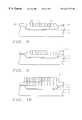
- FIGS. 1 through 10schematically illustrate in cross-sectional representation a preferred embodiment of the present invention.
- the process of the present inventionforms an air well at the substrate underlying the inductor. It is expected that the presence of the air well will reduce substantially the parasitic capacitance and series resistance.
- a field oxide region 12is formed in and on the semiconductor substrate 10 using a conventional local oxidation of silicon (LOCOS) process.
- LOClocal oxidation of silicon
- the field oxidationshould be performed so that the thickness A of the field oxide region into the substrate is between about 2000 and 5000 Angstroms.
- the field oxide region 12is removed by wet etching, for example using a hydrofluoric acid solution, leaving a well 14 in the substrate.
- the depth of the wellis between about 2000 and 5000 Angstroms.
- a thin layer of undoped silicate glass (USG) 16is deposited over the surface of the substrate and lining the well, as shown.
- the USG layer 16has a thickness of between about 1000 and 1500 Angstroms.
- this layer 16may be a stacked nitride-oxide layer, for example 1000 Angstroms of nitride and 500 Angstroms of oxide, or layer 16 may be a thin thermally grown oxide.
- a spin-on-glass layer 18is formed on the substrate and filling the well.
- the spin-on-glass layeris formed as is conventional in the art. That is, a spin-on-glass layer is coated over the wafer by a spin-on method and then baked and cured.
- the spin-on-glass layer 18may be formed by multiple spin-on steps followed by baking and curing of the layers.
- the thickness of the final spin-on-glass film 18may be between about 3000 and 6000 Angstroms.
- the spin-on-glass layer 18is polished back, such as by chemical mechanical polishing (CMP).
- CMPchemical mechanical polishing
- the USG (or other material) layer 16acts as a polish stop.
- the remaining spin-on-glass layer 18has a flat surface just below the surface of the USG layer 16 , as shown in FIG. 4 .
- an oxide layer 20is deposited by chemical vapor deposition (CVD) over the surface of the substrate and over the spin-on-glass-filled well 18 .
- the oxide layerhas a preferred thickness of between about 2000 and 3000 Angstroms.
- a layer of photoresistis coated over the surface of the oxide layer 20 .
- a photoresist mask 25is formed over the oxide using the inductor reticle, as shown in FIG. 6 .
- the oxide 20is etched through to the spin-on-glass layer 18 where the oxide layer is not covered by the photoresist mask 25 using a dry etching process.
- etching chemistriesmay include C 4 F 8 /Co, C 4 F 8 /CHF 3 , or CHF 3 /CF 4 .
- the photoresist mask 25is stripped, for example, using a plasma reactive strip such as O 2 plasma and/or a chemical reactive strip such as H 2 SO 4 /H 2 O 2 .
- a plasma reactive stripsuch as O 2 plasma and/or a chemical reactive strip such as H 2 SO 4 /H 2 O 2 .
- the spin-on-glass 18 underlying the openings 28 within the oxide layeris removed using a dilute hydrofluoric acid (HF) solution having a selectivity of spin-on-glass to oxide of at least 100:1.
- HFdilute hydrofluoric acid
- a thin oxide layeris deposited by chemical vapor deposition (CVD) over the oxide layer 20 .
- This thin oxide layerhaving a thickness of between about 500 and 2000 Angstroms, does not penetrate through the openings 28 into the air well 30 .
- the oxide layerprovides a cap over the openings 28 and together with the first oxide layer 20 forms the oxide layer 32 illustrated in FIG. 9 .
- the thickness of the combined first and second oxide layersis between about 2500 and 5000 Angstroms. This completes formation of the air well 30 within the substrate.
- a layer of metalis deposited and patterned to form the inductor 36 .
- the metalmay be aluminum/copper or copper, for example, and have a thickness of between about 4000 and 10,000 Angstroms.
- the inductor 36may either be a square or a circular spiral.
- the process of the present inventionprovides a method for forming an air well in a silicon substrate underlying the inductor. This process does not involve micro-machining and is simple and compatible with existing processes.
- the inductor fabricated according to the process of the inventioncan have a quality factor (Q) as high as 6 to 7.
Landscapes
- Engineering & Computer Science (AREA)
- Physics & Mathematics (AREA)
- Condensed Matter Physics & Semiconductors (AREA)
- General Physics & Mathematics (AREA)
- Manufacturing & Machinery (AREA)
- Computer Hardware Design (AREA)
- Microelectronics & Electronic Packaging (AREA)
- Power Engineering (AREA)
- Semiconductor Integrated Circuits (AREA)
Abstract
Description
(1) Field of the Invention
The invention relates to a method of forming an inductor in the fabrication of integrated circuits, and more particularly, to a method of forming a high quality inductor using air as a barrier in the manufacture of integrated circuits.
(2) Description of the Prior Art
The integration of radio frequency (RF) integrated circuits on silicon is one of the greatest challenges for the growing markets of wireless communications. The incorporation of RF inductors on silicon without sacrificing the quality factor (Q) due to substrate losses has been researched heavily in recent years. Some of the techniques include: (i) selectively etching out silicon under the inductor by micro-machining, (ii) employing multi-metal layer of aluminum interconnects or copper damascene interconnects, (iii) using a high resistivity silicon substrate, (iv) employing a biased well underneath a spiral inductor, (v) inserting various types of patterned ground shield between the spiral inductor and the silicon substrate, and (vi) increasing the thickness of the interlayer dielectric. This is not an exhaustive listing. The common objectives of all of these techniques are: 1) to enhance the Q value of the inductor and 2) to increase the self-resonance frequency so that the usable frequency range of the inductor is widened.
The self-resonance caused by the parasitic capacitance of the spiral inductor to the silicon substrate will limit the use of these inductors at high frequencies. The increasing series spreading resistance will degrade the Q factor. This impacts the usefulness of integrated spiral inductors implemented on silicon substrates. These problems can be overcome if the area under the inductor is made to appear locally insulating by selectively removing the underlying silicon resulting in inductors “hanging” in air. Air, which has the lowest dielectric constant, is the most ideal barrier. However, micro-machining, used to etch away the silicon under the inductor, is complex and is not compatible with any normal process flow. It is desired to utilize air as a barrier in a process that is implemented easily and is compatible with any process flow with minimal changes.
U.S. Pat. No. 5,539,241 to Abidi et al shows a method of etching out a pit under an inductor during CMOS processing. U.S. Pat. No. 5,844,299 to Merrill et al shows an inductor formed over a pit containing silicon oxide. U.S. Pat. No. 5,742,091 to Hebert et al teaches deep trenches filled with a low dielectric constant material. U.S. Pat. No. 5,773,870 to Su et al discloses backside etching of the substrate under an inductor. U.S. Pat. No. 5,770,509 to Yu et al teaches another inductor process.
A principal objective of the present invention is to provide an effective and very manufacturable method of forming a high quality inductor in the fabrication of integrated circuit devices.
Another objective of the invention is to provide a method of fabricating an inductor utilizing air as an underlying barrier in the manufacture of integrated circuits.
A further objective of the invention is to provide a method of fabricating an inductor having an air well within the silicon substrate thereunder.
In accordance with the objectives of this invention a new method of fabricating an inductor utilizing air as an underlying barrier in the manufacture of integrated circuits is achieved. A field oxide region is formed in and on a semiconductor substrate and then removed whereby a well is left in the semiconductor substrate. A polish stop layer is deposited over the substrate and within the well. The polish stop layer is covered and the well filled with a spin-on-glass layer. The spin-on-glass layer is polished back to the polish stop layer. The polish stop layer is removed. A first oxide layer is deposited overlying the spin-on-glass layer and the semiconductor substrate and is patterned using an inductor reticle whereby a plurality of openings are made through the first oxide layer to the spin-on-glass layer. All of the spin-on-glass layer within the well is removed through the plurality of openings. Thereafter, a second oxide layer is deposited overlying the first oxide layer and capping the plurality of openings thereby forming an air barrier within the well. A metal layer is deposited overlying the second oxide layer and patterned using the same inductor reticle to form the inductor in the fabrication of an integrated circuit device.
In the accompanying drawings forming a material part of this description, there is shown:
FIGS. 1 through 10 schematically illustrate in cross-sectional representation a preferred embodiment of the present invention.
The process of the present invention forms an air well at the substrate underlying the inductor. It is expected that the presence of the air well will reduce substantially the parasitic capacitance and series resistance.
Referring now to FIG. 1, there is shown a portion of asemiconductor substrate 10, preferably composed of monocrystalline silicon. In the first step to form an air well at the substrate underlying an inductor, afield oxide region 12 is formed in and on thesemiconductor substrate 10 using a conventional local oxidation of silicon (LOCOS) process. The field oxidation should be performed so that the thickness A of the field oxide region into the substrate is between about 2000 and 5000 Angstroms.
Next, as shown in FIG. 2, thefield oxide region 12 is removed by wet etching, for example using a hydrofluoric acid solution, leaving awell 14 in the substrate. The depth of the well is between about 2000 and 5000 Angstroms. A thin layer of undoped silicate glass (USG)16 is deposited over the surface of the substrate and lining the well, as shown. TheUSG layer 16 has a thickness of between about 1000 and 1500 Angstroms. Alternatively, thislayer 16 may be a stacked nitride-oxide layer, for example1000 Angstroms of nitride and 500 Angstroms of oxide, orlayer 16 may be a thin thermally grown oxide.
Referring now to FIG. 3, a spin-on-glass layer 18 is formed on the substrate and filling the well. The spin-on-glass layer is formed as is conventional in the art. That is, a spin-on-glass layer is coated over the wafer by a spin-on method and then baked and cured. The spin-on-glass layer 18 may be formed by multiple spin-on steps followed by baking and curing of the layers. The thickness of the final spin-on-glass film 18 may be between about 3000 and 6000 Angstroms.
The spin-on-glass layer 18 is polished back, such as by chemical mechanical polishing (CMP). The USG (or other material)layer 16 acts as a polish stop. The remaining spin-on-glass layer 18 has a flat surface just below the surface of theUSG layer 16, as shown in FIG.4.
Referring now to FIG. 5, anoxide layer 20 is deposited by chemical vapor deposition (CVD) over the surface of the substrate and over the spin-on-glass-filled well18. The oxide layer has a preferred thickness of between about 2000 and 3000 Angstroms.
Next, a layer of photoresist is coated over the surface of theoxide layer 20. Aphotoresist mask 25 is formed over the oxide using the inductor reticle, as shown in FIG.6.
Referring to FIG. 7, theoxide 20 is etched through to the spin-on-glass layer 18 where the oxide layer is not covered by thephotoresist mask 25 using a dry etching process. For example, etching chemistries may include C4F8/Co, C4F8/CHF3, or CHF3/CF4.
Referring now to FIG. 8, thephotoresist mask 25 is stripped, for example, using a plasma reactive strip such as O2plasma and/or a chemical reactive strip such as H2SO4/H2O2. Now, the spin-on-glass 18 underlying theopenings 28 within the oxide layer is removed using a dilute hydrofluoric acid (HF) solution having a selectivity of spin-on-glass to oxide of at least 100:1. After the spin-on-glass 18 has been removed from the well, onlyair 30 remains, as shown in FIG.8.
A thin oxide layer is deposited by chemical vapor deposition (CVD) over theoxide layer 20. This thin oxide layer, having a thickness of between about 500 and 2000 Angstroms, does not penetrate through theopenings 28 into the air well30. The oxide layer provides a cap over theopenings 28 and together with thefirst oxide layer 20 forms theoxide layer 32 illustrated in FIG.9. The thickness of the combined first and second oxide layers is between about 2500 and 5000 Angstroms. This completes formation of the air well30 within the substrate.
Now, as shown in FIG. 10, a layer of metal is deposited and patterned to form theinductor 36. The metal may be aluminum/copper or copper, for example, and have a thickness of between about 4000 and 10,000 Angstroms. Theinductor 36 may either be a square or a circular spiral.
The process of the present invention provides a method for forming an air well in a silicon substrate underlying the inductor. This process does not involve micro-machining and is simple and compatible with existing processes. At a frequency of about 2 gigahertz (GHz), the inductor fabricated according to the process of the invention can have a quality factor (Q) as high as 6 to 7.
While the invention has been particularly shown and described with reference to the preferred embodiments thereof, it will be understood by those skilled in the art that various changes in form and details may be made without departing from the spirit and scope of the invention.
Claims (26)
1. A method of fabricating an inductor in the fabrication of an integrated circuit device comprising:
forming a field oxide region in and on a semiconductor substrate;
removing said field oxide region whereby a well is left in said semiconductor substrate;
depositing a polish stop layer over said substrate and within said well;
covering said polish stop layer and filling said well with a spin-on-glass layer;
polishing back said spin-on-glass layer to said polish stop layer;
depositing a first oxide layer overlying said spin-on-glass layer and said semiconductor substrate;
patterning said first oxide layer using an inductor reticle whereby a plurality of openings are made through said first oxide layer to said spin-on-glass layer;
removing all of said spin-on-glass layer within said well through said plurality of openings;
thereafter depositing a second oxide layer overlying said first oxide layer and capping said plurality of openings thereby forming an air barrier within said well; and
depositing a metal layer overlying said second oxide layer and patterning said metal layer using same said inductor reticle to form said inductor in the fabrication of said integrated circuit.
2. The method according to claim1 wherein said well has a depth of between about 2000 and 5000 Angstroms into said semiconductor substrate.
3. The method according to claim1 wherein said polish stop layer comprises undoped silicon glass having a thickness of between about 1000 and 1500 Angstroms.
4. The method according to claim1 wherein said polish stop layer comprises thermally grown silicon oxide.
5. The method according to claim1 wherein said polish stop layer comprises a stacked silicon nitride/silicon oxide layer having a thickness of between about 1000 and 1500 Angstroms.
6. The method according to claim1 wherein said first oxide layer is deposited to a thickness of between about 2000 and 3000 Angstroms.
7. The method according to claim1 wherein said step of removing said spin-on-glass layer is performed using a dilute hydrofluoric acid solution having a selectivity of spin-on-glass to oxide of at least 100:1.
8. The method according to claim1 wherein said second oxide layer is deposited to a thickness of between about 500 and 2000 Angstroms.
9. The method according to claim1 wherein said metal layer comprises aluminum-copper and is deposited to a thickness of between about 4000 and 10,000 Angstroms.
10. The method according to claim1 wherein said metal layer comprises copper and is deposited to a thickness of between about 4000 and 10,000 Angstroms.
11. The method according to claim1 wherein said inductor has a square shape.
12. The method according to claim1 wherein said inductor has a circular spiral shape.
13. A method of fabricating an inductor in the fabrication of an integrated circuit device comprising:
forming a field oxide region in and on a semiconductor substrate;
removing said field oxide region whereby a well is left in said semiconductor substrate;
depositing an undoped silicate glass layer over said substrate and within said well;
covering said undoped silicate glass layer and filling said well with a spin-on-glass layer;
polishing back said spin-on-glass layer to leave said spin-on-glass layer only within said well wherein said undoped silicate glass layer acts as a polish stop;
depositing a first oxide layer overlying said spinon-glass layer and said semiconductor substrate;
patterning said first oxide layer using an inductor reticle whereby a plurality of openings are made through said first oxide layer to said spin-on-glass layer;
removing all of said spin-on-glass layer within said well through said plurality of openings;
thereafter depositing a second oxide layer overlying said first oxide layer and capping said plurality of openings thereby forming an air barrier within said well; and
depositing a metal layer overlying said second oxide layer and patterning said metal layer using same said inductor reticle to form said inductor in the fabrication of said integrated circuit.
14. The method according to claim13 wherein said well has a depth of between about 2000 and 5000 Angstroms into said semiconductor substrate.
15. The method according to claim13 wherein said undoped silicate glass layer has a thickness of between about 1000 and 1500 Angstroms.
16. The method according to claim13 wherein said first oxide layer is deposited to a thickness of between about 2000 and 3000 Angstroms.
17. The method according to claim13 wherein said step of removing said spin-on-glass layer is performed using a dilute hydrofluoric acid solution having a selectivity of spin-on-glass to oxide of at least 100:1.
18. The method according to claim13 wherein said second oxide layer is deposited to a thickness of between about 500 and 2000 Angstroms.
19. The method according to claim13 wherein said metal layer comprises one of the group containing aluminum-copper and copper and is deposited to a thickness of between about 4000 and 10,000 Angstroms.
20. The method according to claim13 wherein said inductor has a square shape.
21. The method according to claim13 wherein said inductor has a circular spiral shape.
22. A method of fabricating an inductor in the fabrication of an integrated circuit device comprising:
forming a field oxide region in and on a semiconductor substrate;
removing said field oxide region whereby a well is left in said semiconductor substrate;
depositing an undoped silicate glass layer over said substrate and within said well;
covering said undoped silicate glass layer and filling said well with a spin-on-glass layer;
polishing back said spin-on-glass layer to leave said spin-on-glass layer only within said well wherein said undoped silicate glass layer acts as a polish stop;
depositing a first oxide layer overlying said spinon-glass layer and said semiconductor substrate;
patterning said first oxide layer using an inductor reticle whereby a plurality of openings are made through said first oxide layer to said spin-on-glass layer;
removing all of said spin-on-glass layer within said well through said plurality of openings using a dilute hydrofluoric acid solution having a selectivity of spin-on-glass to oxide of at least 100:1;
thereafter depositing a second oxide layer overlying said first oxide layer and capping said plurality of openings thereby forming an air barrier within said well; and
depositing a metal layer overlying said second oxide layer and patterning said metal layer using same said inductor reticle to form said inductor in the fabrication of said integrated circuit.
23. The method according to claim22 wherein said well has a depth of between about 2000 and 5000 Angstroms into said semiconductor substrate.
24. The method according to claim22 wherein the combined thickness of said first and second oxide layers is between about 2500 and 5000 Angstroms.
25. The method according to claim22 wherein said inductor comprises one of the group containing aluminum-copper and copper and has a thickness of between about 4000 and 10,000 Angstroms and wherein said inductor has a circular spiral shape.
26. The method according to claim22 wherein said tor comprises one of the group containing aluminum-copper and has a thickness of between about 4,000 and 10,000 Angstroms and wherein said inductor has a square shape.
Priority Applications (2)
| Application Number | Priority Date | Filing Date | Title |
|---|---|---|---|
| US09/385,524US6221727B1 (en) | 1999-08-30 | 1999-08-30 | Method to trap air at the silicon substrate for improving the quality factor of RF inductors in CMOS technology |
| SG200001839ASG105456A1 (en) | 1999-08-30 | 2000-03-30 | A method to trap air at the silicon substrate for improving the quality factor of rf inductors in cmos technology |
Applications Claiming Priority (1)
| Application Number | Priority Date | Filing Date | Title |
|---|---|---|---|
| US09/385,524US6221727B1 (en) | 1999-08-30 | 1999-08-30 | Method to trap air at the silicon substrate for improving the quality factor of RF inductors in CMOS technology |
Publications (1)
| Publication Number | Publication Date |
|---|---|
| US6221727B1true US6221727B1 (en) | 2001-04-24 |
Family
ID=23521757
Family Applications (1)
| Application Number | Title | Priority Date | Filing Date |
|---|---|---|---|
| US09/385,524Expired - LifetimeUS6221727B1 (en) | 1999-08-30 | 1999-08-30 | Method to trap air at the silicon substrate for improving the quality factor of RF inductors in CMOS technology |
Country Status (2)
| Country | Link |
|---|---|
| US (1) | US6221727B1 (en) |
| SG (1) | SG105456A1 (en) |
Cited By (30)
| Publication number | Priority date | Publication date | Assignee | Title |
|---|---|---|---|---|
| WO2001071809A1 (en)* | 2000-03-17 | 2001-09-27 | Robert Bruce Davies | A die attachment surface having pedestals for receiving components and method of using the attachment |
| US6383889B2 (en)* | 1998-04-10 | 2002-05-07 | Nec Corporation | Semiconductor device having improved parasitic capacitance and mechanical strength |
| US6489663B2 (en)* | 2001-01-02 | 2002-12-03 | International Business Machines Corporation | Spiral inductor semiconducting device with grounding strips and conducting vias |
| US6495903B2 (en)* | 2000-05-25 | 2002-12-17 | Institute Of Microelectronics | Integrated circuit inductor |
| US20030096435A1 (en)* | 2001-02-10 | 2003-05-22 | Acosta Raul E. | High Q inductor with faraday shield and dielectric well buried in substrate |
| US20030146490A1 (en)* | 2002-02-07 | 2003-08-07 | Semiconductor Components Industries, Llc. | Semiconductor device and method of providing regions of low substrate capacitance |
| US20030153171A1 (en)* | 2002-02-13 | 2003-08-14 | Gu-Sung Kim | Wafer level package with air pads and manufacturing method thereof |
| US6661068B2 (en) | 2002-03-20 | 2003-12-09 | Semiconductor Components Industries Llc | Semiconductor device and method of providing regions of low substrate capacitance |
| US20040084750A1 (en)* | 2000-08-01 | 2004-05-06 | Ahn Kie Y. | Low loss high Q inductor |
| US20040245580A1 (en)* | 1998-12-21 | 2004-12-09 | Mou-Shiung Lin | [chip structure with a passive device and method for forming the same] |
| US6917091B2 (en) | 2003-03-28 | 2005-07-12 | Mitsubishi Denki Kabushiki Kaisha | High power semiconductor device having source electrodes connected by air bridges and having opposite current path directions |
| US20050173777A1 (en)* | 2004-02-09 | 2005-08-11 | Semiconductor Components Industries, Llc | Semiconductor device having reduced capacitance to substrate and method |
| US20050184358A1 (en)* | 1998-12-21 | 2005-08-25 | Megic Corporation | High performance system-on-chip using post passivation process |
| US20060001124A1 (en)* | 2004-07-02 | 2006-01-05 | Georgia Tech Research Corporation | Low-loss substrate for high quality components |
| US7148553B1 (en) | 2001-08-01 | 2006-12-12 | Davies Robert B | Semiconductor device with inductive component and method of making |
| US20070202684A1 (en)* | 2003-05-27 | 2007-08-30 | Megica Corporation | High performance system-on-chip inductor using post passivation process |
| US20070262456A1 (en)* | 1998-12-21 | 2007-11-15 | Mou-Shiung Lin | Top layers of metal for high performance IC's |
| CN100465786C (en)* | 2004-08-24 | 2009-03-04 | 华新丽华股份有限公司 | Optical microelectromechanical element and manufacturing method thereof |
| US20090184394A1 (en)* | 1998-12-21 | 2009-07-23 | Megica Corporation | High performance system-on-chip inductor using post passivation process |
| US20100078760A1 (en)* | 2008-09-30 | 2010-04-01 | Freescale Semiconductor, Inc. | Integrated circuit module with integrated passive device |
| US20100165585A1 (en)* | 2008-12-26 | 2010-07-01 | Megica Corporation | Chip packages with power management integrated circuits and related techniques |
| US7960269B2 (en) | 2005-07-22 | 2011-06-14 | Megica Corporation | Method for forming a double embossing structure |
| US7973629B2 (en) | 2001-09-04 | 2011-07-05 | Megica Corporation | Method for making high-performance RF integrated circuits |
| US8008775B2 (en) | 2004-09-09 | 2011-08-30 | Megica Corporation | Post passivation interconnection structures |
| US8018060B2 (en) | 2004-09-09 | 2011-09-13 | Megica Corporation | Post passivation interconnection process and structures |
| US8178435B2 (en) | 1998-12-21 | 2012-05-15 | Megica Corporation | High performance system-on-chip inductor using post passivation process |
| US8384189B2 (en) | 2005-03-29 | 2013-02-26 | Megica Corporation | High performance system-on-chip using post passivation process |
| US8749021B2 (en) | 2006-12-26 | 2014-06-10 | Megit Acquisition Corp. | Voltage regulator integrated with semiconductor chip |
| US8907227B2 (en) | 2012-08-02 | 2014-12-09 | Hong Kong Science and Technology Research Institute Company Limited | Multiple surface integrated devices on low resistivity substrates |
| DE102010000895B4 (en)* | 2010-01-14 | 2018-12-27 | Robert Bosch Gmbh | A method of making a via of a semiconductor device having a surrounding annular isolation trench and corresponding semiconductor device |
Citations (8)
| Publication number | Priority date | Publication date | Assignee | Title |
|---|---|---|---|---|
| US5539241A (en) | 1993-01-29 | 1996-07-23 | The Regents Of The University Of California | Monolithic passive component |
| US5742091A (en) | 1995-07-12 | 1998-04-21 | National Semiconductor Corporation | Semiconductor device having a passive device formed over one or more deep trenches |
| US5770509A (en) | 1996-12-06 | 1998-06-23 | Electronics & Telecommunications Research Institute | Method for forming an inductor devices using substrate biasing technique |
| US5773870A (en) | 1996-09-10 | 1998-06-30 | National Science Council | Membrane type integrated inductor and the process thereof |
| US5844299A (en) | 1997-01-31 | 1998-12-01 | National Semiconductor Corporation | Integrated inductor |
| US5856703A (en)* | 1995-12-27 | 1999-01-05 | Micron Technology, Inc. | Integrated circuitry having a pair of adjacent conductive lines |
| US6081030A (en)* | 1997-06-27 | 2000-06-27 | Stmicroelectronics S.A. | Semiconductor device having separated exchange means |
| US6140197A (en)* | 1999-08-30 | 2000-10-31 | Chartered Semiconductor Manufacturing Ltd. | Method of making spiral-type RF inductors having a high quality factor (Q) |
- 1999
- 1999-08-30USUS09/385,524patent/US6221727B1/ennot_activeExpired - Lifetime
- 2000
- 2000-03-30SGSG200001839Apatent/SG105456A1/enunknown
Patent Citations (8)
| Publication number | Priority date | Publication date | Assignee | Title |
|---|---|---|---|---|
| US5539241A (en) | 1993-01-29 | 1996-07-23 | The Regents Of The University Of California | Monolithic passive component |
| US5742091A (en) | 1995-07-12 | 1998-04-21 | National Semiconductor Corporation | Semiconductor device having a passive device formed over one or more deep trenches |
| US5856703A (en)* | 1995-12-27 | 1999-01-05 | Micron Technology, Inc. | Integrated circuitry having a pair of adjacent conductive lines |
| US5773870A (en) | 1996-09-10 | 1998-06-30 | National Science Council | Membrane type integrated inductor and the process thereof |
| US5770509A (en) | 1996-12-06 | 1998-06-23 | Electronics & Telecommunications Research Institute | Method for forming an inductor devices using substrate biasing technique |
| US5844299A (en) | 1997-01-31 | 1998-12-01 | National Semiconductor Corporation | Integrated inductor |
| US6081030A (en)* | 1997-06-27 | 2000-06-27 | Stmicroelectronics S.A. | Semiconductor device having separated exchange means |
| US6140197A (en)* | 1999-08-30 | 2000-10-31 | Chartered Semiconductor Manufacturing Ltd. | Method of making spiral-type RF inductors having a high quality factor (Q) |
Cited By (66)
| Publication number | Priority date | Publication date | Assignee | Title |
|---|---|---|---|---|
| US6383889B2 (en)* | 1998-04-10 | 2002-05-07 | Nec Corporation | Semiconductor device having improved parasitic capacitance and mechanical strength |
| US20070267714A1 (en)* | 1998-12-21 | 2007-11-22 | Mou-Shiung Lin | Top layers of metal for high performance IC's |
| US8178435B2 (en) | 1998-12-21 | 2012-05-15 | Megica Corporation | High performance system-on-chip inductor using post passivation process |
| US20070290358A1 (en)* | 1998-12-21 | 2007-12-20 | Mou-Shiung Lin | Top layers of metal for high performance IC's |
| US7422941B2 (en) | 1998-12-21 | 2008-09-09 | Megica Corporation | High performance system-on-chip using post passivation process |
| US8531038B2 (en) | 1998-12-21 | 2013-09-10 | Megica Corporation | Top layers of metal for high performance IC's |
| US8487400B2 (en) | 1998-12-21 | 2013-07-16 | Megica Corporation | High performance system-on-chip using post passivation process |
| US8471384B2 (en) | 1998-12-21 | 2013-06-25 | Megica Corporation | Top layers of metal for high performance IC's |
| US20080111243A1 (en)* | 1998-12-21 | 2008-05-15 | Megica Corporation | High performance system-on-chip using post passivation process |
| US20080044976A1 (en)* | 1998-12-21 | 2008-02-21 | Megica Corporation | High performance system-on-chip using post passivation process |
| US8022545B2 (en) | 1998-12-21 | 2011-09-20 | Megica Corporation | Top layers of metal for high performance IC's |
| US20040245580A1 (en)* | 1998-12-21 | 2004-12-09 | Mou-Shiung Lin | [chip structure with a passive device and method for forming the same] |
| US20080035972A1 (en)* | 1998-12-21 | 2008-02-14 | Megica Corporation | High performance system-on-chip using post passivation process |
| US8421158B2 (en) | 1998-12-21 | 2013-04-16 | Megica Corporation | Chip structure with a passive device and method for forming the same |
| US8415800B2 (en) | 1998-12-21 | 2013-04-09 | Megica Corporation | Top layers of metal for high performance IC's |
| US20050184358A1 (en)* | 1998-12-21 | 2005-08-25 | Megic Corporation | High performance system-on-chip using post passivation process |
| US20080038869A1 (en)* | 1998-12-21 | 2008-02-14 | Megica Corporation | High performance system-on-chip using post passivation process |
| US7999384B2 (en) | 1998-12-21 | 2011-08-16 | Megica Corporation | Top layers of metal for high performance IC's |
| US20080042238A1 (en)* | 1998-12-21 | 2008-02-21 | Megica Corporation | High performance system-on-chip using post passivation process |
| US20070284752A1 (en)* | 1998-12-21 | 2007-12-13 | Mou-Shiung Lin | Top layers of metal for high performance IC's |
| US20070278686A1 (en)* | 1998-12-21 | 2007-12-06 | Mou-Shiung Lin | Top layers of metal for high performance IC's |
| US7884479B2 (en) | 1998-12-21 | 2011-02-08 | Megica Corporation | Top layers of metal for high performance IC's |
| US7863654B2 (en) | 1998-12-21 | 2011-01-04 | Megica Corporation | Top layers of metal for high performance IC's |
| US20090184394A1 (en)* | 1998-12-21 | 2009-07-23 | Megica Corporation | High performance system-on-chip inductor using post passivation process |
| US20090045516A1 (en)* | 1998-12-21 | 2009-02-19 | Megica Corporation | TOP LAYERS OF METAL FOR HIGH PERFORMANCE IC's |
| US20070262456A1 (en)* | 1998-12-21 | 2007-11-15 | Mou-Shiung Lin | Top layers of metal for high performance IC's |
| US20070262457A1 (en)* | 1998-12-21 | 2007-11-15 | Mou-Shiung Lin | Top layers of metal for high performance IC's |
| US7459761B2 (en)* | 1998-12-21 | 2008-12-02 | Megica Corporation | High performance system-on-chip using post passivation process |
| WO2001071809A1 (en)* | 2000-03-17 | 2001-09-27 | Robert Bruce Davies | A die attachment surface having pedestals for receiving components and method of using the attachment |
| US6908825B2 (en) | 2000-05-25 | 2005-06-21 | Institute Of Microelectronics | Method of making an integrated circuit inductor wherein a plurality of apertures are formed beneath an inductive loop |
| US6495903B2 (en)* | 2000-05-25 | 2002-12-17 | Institute Of Microelectronics | Integrated circuit inductor |
| US6806805B2 (en)* | 2000-08-01 | 2004-10-19 | Micron Technology, Inc. | Low loss high Q inductor |
| US20040084750A1 (en)* | 2000-08-01 | 2004-05-06 | Ahn Kie Y. | Low loss high Q inductor |
| US6489663B2 (en)* | 2001-01-02 | 2002-12-03 | International Business Machines Corporation | Spiral inductor semiconducting device with grounding strips and conducting vias |
| US6762088B2 (en)* | 2001-02-10 | 2004-07-13 | International Business Machines Corporation | High Q inductor with faraday shield and dielectric well buried in substrate |
| US20030096435A1 (en)* | 2001-02-10 | 2003-05-22 | Acosta Raul E. | High Q inductor with faraday shield and dielectric well buried in substrate |
| US7148553B1 (en) | 2001-08-01 | 2006-12-12 | Davies Robert B | Semiconductor device with inductive component and method of making |
| US20110175195A1 (en)* | 2001-09-04 | 2011-07-21 | Megica Corporation | Method for making high-performance rf integrated circuits |
| US8384508B2 (en) | 2001-09-04 | 2013-02-26 | Megica Corporation | Method for making high-performance RF integrated circuits |
| US7973629B2 (en) | 2001-09-04 | 2011-07-05 | Megica Corporation | Method for making high-performance RF integrated circuits |
| US20030146490A1 (en)* | 2002-02-07 | 2003-08-07 | Semiconductor Components Industries, Llc. | Semiconductor device and method of providing regions of low substrate capacitance |
| US20070085219A1 (en)* | 2002-02-13 | 2007-04-19 | Samsung Electronics Co., Ltd. | Method for manufacture of wafer level package with air pads |
| US7550317B2 (en) | 2002-02-13 | 2009-06-23 | Samsung Electronics Co., Ltd. | Method for manufacture of wafer level package with air pads |
| US20030153171A1 (en)* | 2002-02-13 | 2003-08-14 | Gu-Sung Kim | Wafer level package with air pads and manufacturing method thereof |
| DE10301432B4 (en)* | 2002-02-13 | 2007-10-18 | Samsung Electronics Co., Ltd., Suwon | Interconnect structure in a wafer-level package and manufacturing process |
| US7141885B2 (en) | 2002-02-13 | 2006-11-28 | Samsung Electronics Co., Ltd. | Wafer level package with air pads and manufacturing method thereof |
| CN100336195C (en)* | 2002-03-20 | 2007-09-05 | 半导体元件工业有限责任公司 | Semiconductor device and method for providing low substrate capacitor area |
| US6661068B2 (en) | 2002-03-20 | 2003-12-09 | Semiconductor Components Industries Llc | Semiconductor device and method of providing regions of low substrate capacitance |
| US6917091B2 (en) | 2003-03-28 | 2005-07-12 | Mitsubishi Denki Kabushiki Kaisha | High power semiconductor device having source electrodes connected by air bridges and having opposite current path directions |
| US20070202685A1 (en)* | 2003-05-27 | 2007-08-30 | Megica Corporation | High performance system-on-chip inductor using post passivation process |
| US20070202684A1 (en)* | 2003-05-27 | 2007-08-30 | Megica Corporation | High performance system-on-chip inductor using post passivation process |
| US7087925B2 (en) | 2004-02-09 | 2006-08-08 | Semiconductor Components Industries, L.L.C. | Semiconductor device having reduced capacitance to substrate and method |
| US20050173777A1 (en)* | 2004-02-09 | 2005-08-11 | Semiconductor Components Industries, Llc | Semiconductor device having reduced capacitance to substrate and method |
| US20060001124A1 (en)* | 2004-07-02 | 2006-01-05 | Georgia Tech Research Corporation | Low-loss substrate for high quality components |
| CN100465786C (en)* | 2004-08-24 | 2009-03-04 | 华新丽华股份有限公司 | Optical microelectromechanical element and manufacturing method thereof |
| US8008775B2 (en) | 2004-09-09 | 2011-08-30 | Megica Corporation | Post passivation interconnection structures |
| US8018060B2 (en) | 2004-09-09 | 2011-09-13 | Megica Corporation | Post passivation interconnection process and structures |
| US8384189B2 (en) | 2005-03-29 | 2013-02-26 | Megica Corporation | High performance system-on-chip using post passivation process |
| US7960269B2 (en) | 2005-07-22 | 2011-06-14 | Megica Corporation | Method for forming a double embossing structure |
| US8749021B2 (en) | 2006-12-26 | 2014-06-10 | Megit Acquisition Corp. | Voltage regulator integrated with semiconductor chip |
| US20100078760A1 (en)* | 2008-09-30 | 2010-04-01 | Freescale Semiconductor, Inc. | Integrated circuit module with integrated passive device |
| US7763976B2 (en) | 2008-09-30 | 2010-07-27 | Freescale Semiconductor, Inc. | Integrated circuit module with integrated passive device |
| US20100165585A1 (en)* | 2008-12-26 | 2010-07-01 | Megica Corporation | Chip packages with power management integrated circuits and related techniques |
| US8809951B2 (en) | 2008-12-26 | 2014-08-19 | Megit Acquisition Corp. | Chip packages having dual DMOS devices with power management integrated circuits |
| DE102010000895B4 (en)* | 2010-01-14 | 2018-12-27 | Robert Bosch Gmbh | A method of making a via of a semiconductor device having a surrounding annular isolation trench and corresponding semiconductor device |
| US8907227B2 (en) | 2012-08-02 | 2014-12-09 | Hong Kong Science and Technology Research Institute Company Limited | Multiple surface integrated devices on low resistivity substrates |
Also Published As
| Publication number | Publication date |
|---|---|
| SG105456A1 (en) | 2004-08-27 |
Similar Documents
| Publication | Publication Date | Title |
|---|---|---|
| US6221727B1 (en) | Method to trap air at the silicon substrate for improving the quality factor of RF inductors in CMOS technology | |
| US6140197A (en) | Method of making spiral-type RF inductors having a high quality factor (Q) | |
| US6274920B1 (en) | Integrated inductor device and method for fabricating the same | |
| US5728621A (en) | Method for shallow trench isolation | |
| US6057202A (en) | Method for manufacturing an inductor with resonant frequency and Q value increased in semiconductor process | |
| KR100421055B1 (en) | Method for forming metal interconnection layer of semiconductor device | |
| US5010039A (en) | Method of forming contacts to a semiconductor device | |
| US5654216A (en) | Formation of a metal via structure from a composite metal layer | |
| US6399461B1 (en) | Addition of planarizing dielectric layer to reduce a dishing phenomena experienced during a chemical mechanical procedure used in the formation of shallow trench isolation regions | |
| JPH09162354A (en) | Integrated inductor structure and its manufacture | |
| TW200524128A (en) | A device and method for providing shielding in radio frequency integrated circuits to reduce noise coupling | |
| US6261923B1 (en) | Method to solve the dishing issue in CMP planarization by using a nitride hard mask for local inverse etchback and CMP | |
| CN112614833A (en) | Groove type capacitor device and preparation method thereof | |
| US6406992B1 (en) | Fabrication method for a dual damascene structure | |
| US6825080B1 (en) | Method for forming a MIM capacitor | |
| KR100234416B1 (en) | Method of forming a device isolation film of semiconductor device | |
| CN100390926C (en) | Method for manufacturing contact region on Silicon On Insulator (SOI) wafer | |
| US6133113A (en) | Method of manufacturing shallow trench isolation | |
| US6486017B1 (en) | Method of reducing substrate coupling for chip inductors by creation of dielectric islands by selective EPI deposition | |
| JP7703458B2 (en) | Integrated circuits including composite dielectric layers - Patents.com | |
| US6794269B1 (en) | Method for and structure formed from fabricating a relatively deep isolation structure | |
| US6518141B2 (en) | Method for manufacturing a radio frequency integrated circuit on epitaxial silicon | |
| JPH10116904A (en) | Manufacture of semiconductor device | |
| US20040229442A1 (en) | Method for forming high resistive region in semiconductor device | |
| US6214735B1 (en) | Method for planarizing a semiconductor substrate |
Legal Events
| Date | Code | Title | Description |
|---|---|---|---|
| AS | Assignment | Owner name:NATIONAL UNIVERSITY OF SINGAPORE, SINGAPORE Free format text:ASSIGNMENT OF ASSIGNORS INTEREST;ASSIGNORS:CHAN, LAP;CHEW, JOHNNY KOK WAI;CHA, CHER LIANG;AND OTHERS;REEL/FRAME:010208/0689 Effective date:19990730 Owner name:CHARTERED SEMICONDUCOR MANUFACTURING, LTD., SINGAP Free format text:ASSIGNMENT OF ASSIGNORS INTEREST;ASSIGNORS:CHAN, LAP;CHEW, JOHNNY KOK WAI;CHA, CHER LIANG;AND OTHERS;REEL/FRAME:010208/0689 Effective date:19990730 | |
| STCF | Information on status: patent grant | Free format text:PATENTED CASE | |
| CC | Certificate of correction | ||
| FPAY | Fee payment | Year of fee payment:4 | |
| FPAY | Fee payment | Year of fee payment:8 | |
| FPAY | Fee payment | Year of fee payment:12 |