US6220934B1 - Method for controlling pH during planarization and cleaning of microelectronic substrates - Google Patents
Method for controlling pH during planarization and cleaning of microelectronic substratesDownload PDFInfo
- Publication number
- US6220934B1 US6220934B1US09/122,187US12218798AUS6220934B1US 6220934 B1US6220934 B1US 6220934B1US 12218798 AUS12218798 AUS 12218798AUS 6220934 B1US6220934 B1US 6220934B1
- Authority
- US
- United States
- Prior art keywords
- planarizing
- microelectronic substrate
- fluid
- polishing pad
- approximately
- Prior art date
- Legal status (The legal status is an assumption and is not a legal conclusion. Google has not performed a legal analysis and makes no representation as to the accuracy of the status listed.)
- Expired - Lifetime
Links
Images


Classifications
- B—PERFORMING OPERATIONS; TRANSPORTING
- B24—GRINDING; POLISHING
- B24B—MACHINES, DEVICES, OR PROCESSES FOR GRINDING OR POLISHING; DRESSING OR CONDITIONING OF ABRADING SURFACES; FEEDING OF GRINDING, POLISHING, OR LAPPING AGENTS
- B24B57/00—Devices for feeding, applying, grading or recovering grinding, polishing or lapping agents
- B24B57/02—Devices for feeding, applying, grading or recovering grinding, polishing or lapping agents for feeding of fluid, sprayed, pulverised, or liquefied grinding, polishing or lapping agents
- B—PERFORMING OPERATIONS; TRANSPORTING
- B24—GRINDING; POLISHING
- B24B—MACHINES, DEVICES, OR PROCESSES FOR GRINDING OR POLISHING; DRESSING OR CONDITIONING OF ABRADING SURFACES; FEEDING OF GRINDING, POLISHING, OR LAPPING AGENTS
- B24B37/00—Lapping machines or devices; Accessories
- B24B37/005—Control means for lapping machines or devices
- B24B37/0056—Control means for lapping machines or devices taking regard of the pH-value of lapping agents
- B—PERFORMING OPERATIONS; TRANSPORTING
- B24—GRINDING; POLISHING
- B24B—MACHINES, DEVICES, OR PROCESSES FOR GRINDING OR POLISHING; DRESSING OR CONDITIONING OF ABRADING SURFACES; FEEDING OF GRINDING, POLISHING, OR LAPPING AGENTS
- B24B37/00—Lapping machines or devices; Accessories
- B24B37/04—Lapping machines or devices; Accessories designed for working plane surfaces
- B24B37/042—Lapping machines or devices; Accessories designed for working plane surfaces operating processes therefor
- B—PERFORMING OPERATIONS; TRANSPORTING
- B24—GRINDING; POLISHING
- B24B—MACHINES, DEVICES, OR PROCESSES FOR GRINDING OR POLISHING; DRESSING OR CONDITIONING OF ABRADING SURFACES; FEEDING OF GRINDING, POLISHING, OR LAPPING AGENTS
- B24B49/00—Measuring or gauging equipment for controlling the feed movement of the grinding tool or work; Arrangements of indicating or measuring equipment, e.g. for indicating the start of the grinding operation
- H—ELECTRICITY
- H01—ELECTRIC ELEMENTS
- H01L—SEMICONDUCTOR DEVICES NOT COVERED BY CLASS H10
- H01L21/00—Processes or apparatus adapted for the manufacture or treatment of semiconductor or solid state devices or of parts thereof
- H01L21/02—Manufacture or treatment of semiconductor devices or of parts thereof
- H01L21/02002—Preparing wafers
- H01L21/02005—Preparing bulk and homogeneous wafers
- H01L21/02008—Multistep processes
- H01L21/0201—Specific process step
- H01L21/02024—Mirror polishing
- H—ELECTRICITY
- H01—ELECTRIC ELEMENTS
- H01L—SEMICONDUCTOR DEVICES NOT COVERED BY CLASS H10
- H01L21/00—Processes or apparatus adapted for the manufacture or treatment of semiconductor or solid state devices or of parts thereof
- H01L21/02—Manufacture or treatment of semiconductor devices or of parts thereof
- H01L21/02041—Cleaning
- H01L21/02043—Cleaning before device manufacture, i.e. Begin-Of-Line process
- H01L21/02052—Wet cleaning only
Definitions
- the present inventionrelates to mechanical and chemical-mechanical planarization of microelectronic substrates. More particularly, the present invention relates to controlling the pH of a microelectronic substrate during planarization and post-planarization processing of the microelectronic substrate.
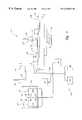
- FIG. Ischematically illustrates a planarizing machine 10 with a platen or base 20 , a carrier assembly 30 , a polishing pad 41 positioned on the platen 20 , and a planarizing liquid 44 on the polishing pad 41 .
- the planarizing machine 10can also have an under-pad 25 attached to an upper surface 22 of the platen 20 for supporting the polishing pad 41 .
- a drive assembly 26rotates (arrow A) and/or reciprocates (arrow B) the platen 20 to move the polishing pad 41 during planarization.
- the carrier assembly 30controls and protects a substrate 12 during planarization.
- the carrier assembly 30generally has a substrate holder 32 with a pad 34 that holds the substrate 12 via suction.
- a carrier drive assembly 36typically rotates and/or translates the substrate holder 32 (arrows C and D, respectively).
- the substrate holder 32can include a weighted, free-floating disk (not shown) that slides over the polishing pad 41 .
- the combination of the polishing pad 41 and the planarizing liquid 44generally defines a planarizing medium 40 that mechanically and/or chemically-mechanically removes material from the surface of the substrate 12 .
- the polishing pad 41may be a conventional polishing pad composed of a polymeric material (e.g., polyurethane) without abrasive particles, or it may be an abrasive polishing pad with abrasive particles fixedly bonded to a suspension material.
- the planarizing liquid 44may be a chemical-mechanical planarization slurry with abrasive particles and chemicals for use with a conventional non-abrasive polishing pad.
- the planarizing liquid 44may be a chemical solution without abrasive particles for use with an abrasive polishing pad.
- the planarizing liquid 44can be pumped from a planarizing liquid supply 45 through a conduit 46 , and through orifices 43 to a planarizing surface 42 of the polishing pad 41 .
- the carrier assembly 30presses the substrate 12 against the planarizing surface 42 of the polishing pad 41 in the presence of the planarizing liquid 44 .
- the platen 20 and/or the substrate holder 32then move relative to one another to translate the substrate 12 across the planarizing surface 42 .
- the abrasive particles and/or the chemicals of the planarizing medium 40remove material from the surface of the substrate 12 .
- particulate mattersuch as abrasive particles, particles removed from the polishing pad 41 , and/or particles removed from the substrate 12 may adhere to the substrate. Accordingly, the substrate 12 can be rinsed to remove the particulate matter before the substrate 12 undergoes additional processing.
- One conventional approach to rinsing the substrate 12is to pump a rinsing solution 53 from a rinsing solution supply 54 through the orifices 43 to the planarizing surface 42 of the polishing pad 41 .
- the rinsing solution 53rinses the substrate 12 while the substrate remains in situ on the polishing pad 41 .
- the rinsing solution 53may be introduced to the polishing pad 41 as the relative velocity between the substrate 12 and the polishing pad 41 is reduced or ramped down.
- the substrate transporter 60can include a grasping device 62 that engages the substrate 12 after the substrate has been detached from the carrier assembly 30 .
- the substrate transporter 60can further include one or more movable arms 61 that can robotically move the substrate 12 to the rinse chamber 50 .
- the rinse chamber 50can include a plurality of opposing spray bars 51 , each having a plurality of nozzles 52 for directing a spray of the rinsing solution 53 onto the substrate 12 .
- the rinse chamber 50 shown in FIG. 1can simultaneously accommodate two substrates 12 positioned upright in adjacent bays 57 .
- a third approach to removing particulate matter from the substrate 12is to remove the substrate from the polishing pad 41 and place the substrate 12 on a separate buffing pad (not shown).
- the buffing padthen moves relative to the substrate and may also be supplied with a rinsing solution to convey the particulate matter away.
- the planarizing machine 10can include a conditioner 70 that removes polishing pad material from the planarizing surface 42 to expose new polishing pad material.
- the conditioner 70can include an abrasive disk 71 for mechanically roughening the planarizing surface 42 of the polishing pad 41 .
- the conditioner 70can also include a conditioning fluid source 72 that supplies conditioning fluid to the polishing pad 41 for chemically conditioning the planarizing surface 42 of the polishing pad 41 .
- Planarizing processesmust consistently and accurately produce a uniformly planar surface on the microelectronic substrate 12 to enable precise fabrication of circuits and photo-patterns. As the density of integrated circuits increases, the uniformity and planarity of the substrate surface is becoming increasingly important because it is difficult to form sub-micron features or photo-patterns to within a tolerance of approximately 0.1 microns on non-uniform substrate surfaces. Thus, planarizing processes must create a highly uniform, planar surface on the substrate.
- planarizing solutionis an ammonia-based solution
- the rinsing and conditioning fluidsare deionized water.
- Each chemical solutionmay have different chemical characteristics and sequentially exposing the microelectronic substrate 12 to different chemical solutions may cause particulates to adhere to the surfaces of the substrate. These particulates may damage the wafer during subsequent polishing and handling steps, or may interfere with subsequent processing steps, such as masking and etching. Furthermore, the particulates may become incorporated into the devices formed on the substrate, potentially causing the devices to fail.
- the apparatuscan include a polishing pad having a planarizing surface and a source of planarizing liquid in fluid communication with the planarizing surface of the polishing pad.
- the microelectronic substrateis planarized by engaging the substrate with the polishing pad while the planarizing liquid is disposed on the polishing pad, and moving one of the substrate and the polishing pad relative to the other of the substrate and the polishing pad. As the relative motion between the substrate and the polishing pad is decreased, rinsing fluid having a pH approximately the same as a pH of the planarizing liquid can be introduced to the planarizing surface to maintain the pH of the microelectronic substrate at an approximately constant level.
- the microelectronic substratecan be removed from the polishing pad and rinsed remotely with a rinsing liquid having a pH approximately the same as a pH of the planarizing liquid.
- the rinsing liquid in either of the foregoing embodimentscan be selected to include tetramethyl ammonium hydroxide and deionized water, or other substances where a pH of the rinsing liquid is approximately the same as the pH of the planarizing liquid.
- the polishing padcan include a nonabrasive polishing pad and the planarizing liquid can include an abrasive slurry.
- the pH of the microelectronic substratecan be maintained by maintaining the pH of the abrasive slurry at an approximately constant level as the relative velocity between the microelectronic substrate and the polishing pad is reduced to approximately zero.
- the polishing padcan be conditioned by supplying to the polishing pad a conditioning liquid having a pH approximately the same as the pH of the planarizing liquid.
- the microelectronic substratecan be cleaned by engaging the microelectronic substrate with the polishing pad, after the polishing pad has been conditioned, and moving at least one of the polishing pad and the substrate relative to the other of the polishing pad and the substrate.
- FIG. 1is a schematic side elevation view of a planarizing machine in accordance with the prior art.
- FIG. 2is a schematic side elevation view of a planarizing machine having a source of rinsing liquid and a source of planarizing liquid, each liquid having an approximately equal pH in accordance with an embodiment of the present invention.
- FIG. 3is a schematic side elevation view of a planarizing machine having a source of conditioning liquid and a source of planarizing liquid, each liquid having an approximately equal pH in accordance with another embodiment of the present invention.
- the present inventionis an apparatus and method for mechanical and/or chemical-mechanical planarization of substrates used in the manufacture of microelectronic devices. Many specific details of certain embodiments of the present invention are set forth in the following description and in FIGS. 2-3 to provide a thorough understanding of such embodiments. One skilled in the ail, however, will understand that the present invention may have additional embodiments or that the invention may be practiced without several of the details described in the following description.
- FIG. 2is a schematic side elevation view of a CMP machine 110 having a platen 120 and a planarizing medium 140 .
- the CMP machinecan include a model number 676 manufactured by IPEC Corp. of Portland, Oreg., and in other embodiments, the CMP machine can include other devices, such as a web-format plananizing machine, manufactured by EDC Corporation.
- the planarizing medium 140includes a polishing pad 141 and an under-pad 125 releasably attached to the platen 120 .
- the planarizing mediumcan further include a planarizing liquid 144 disposed on a planarizing surface 142 of the polishing pad 141 .
- the platen 120can be movable by means of a platen drive assembly 126 that can impart a rotational motion (indicated by arrow A) and/or a translational motion (indicated by arrow B) to the platen 120 .
- the CMP apparatus 110can also include a carrier assembly 130 having a substrate holder 132 and a resilient pad 134 that together press a microelectronic substrate 112 against the planarizing surface 142 of the polishing pad 141 .
- a carrier drive assembly 136can be coupled to the carrier assembly 130 to move the carrier assembly axially (indicated by arrow C) and/or rotationally (indicated by arrow D) relative to the platen 120 .
- the planarizing liquid 144can be supplied to the polishing pad 141 from a planarizing liquid supply 145 via a conduit 146 .
- the conduit 146can include a flexible coupling 147 , shown schematically in FIG. 2, to allow for translational or rotational motion of the platen 120 relative to the planarizing liquid supply 145 .
- the coupling 147can be connected to a manifold 148 in the platen 120 .
- the manifold 148can include a plurality of orifices 143 that extend upwardly through the under-pad 145 and the polishing pad 141 to the planarizing surface 142 of the polishing pad.
- the planarizing medium 140i.e., the polishing pad 141 and/or the planarizing liquid 144 . removes material from the microelectronic substrate 112 . The process may also cause material to be removed from the polishing pad 141 .
- the CMP machine 110can include a rinsing liquid 153 that is pumped from a rinsing liquid supply 154 through the conduit 146 to the orifices 143 in the polishing pad 141 .
- the conduit 146can include a valve 149 that can be adjusted to couple the rinsing liquid supply 154 and/or the planarizing liquid supply 145 with the orifices 143 , to selectively provide rinsing liquid 153 and/or planarizing fluid 144 to the polishing pad 141 .
- the rinsing liquid 153is selected to have a pH approximately the same as a pH of the planarizing liquid 144 , to maintain the pH of the substrate 112 at an approximately constant level as the substrate 112 is exposed to the rinsing liquid 153 .
- the CMP machine 110can include a pH meter 158 coupled to the rinsing liquid supply 154 and the planarizing liquid supply 145 to monitor the pH levels of both liquids.
- the pH metercan include a conductivity meter or other device that detects pH.
- the planarizing liquid 144can include Klebosol, an ammonia-based solution available from Rodel Corp. of Newark, Del. having a pH in the range of approximately 10.6 to approximately 11.4, and more particularly, approximately 11.0.
- the pH of the rinsing liquid 153can be selected to have a pH in approximately the same range.
- the rinsing liquid 153can include a mixture of deionized water provided by a deionized water supply 155 and tetramethyl ammonium hydroxide (TMAH) provided by a TMAH supply 156 .
- TMAHtetramethyl ammonium hydroxide
- the relative amount of deionized water and TMAH included in the rinsing liquid 153can be controlled by adjusting a rinsing liquid valve 157 coupled between the deionized water supply 155 and the TMAH supply 156 .
- the rinsing liquid 153can include 99.994% deionized water and 0.006% TMAH by volume, to have a pH of approximately 11.0.
- the planarizing liquid 144 and the rinsing liquid 153can include other compositions having other pHs, so long as the pH of the rinsing liquid 153 is selected to be approximately the same as the pH of the planarizing liquid 144 .
- the rinsing liquid 153can be selected to have an electrical charge that is approximately the same as an electric charge of the planarizing liquid 144 .
- the electrical charge of the rinsing liquid 153 and the planarizing liquid 144can be selected to be approximately zero to reduce the likelihood of imparting unwanted electrical charges to the substrate 112 .
- the substrate 112 , the rinsing liquid 153 , and/or the planarizing liquid 144can have other non-zero electrical charges.
- the CMP machine 110can also include a substrate transporter 160 and a rinse chamber 150 .
- the substrate transporter 160can include a plurality of articulated movable arms 161 coupled to a grasping device 162 .
- the grasping device 162can engage the substrate 112 after it has been released from the carrier assembly 130 and the arms 161 can be controlled to robotically transfer the substrate 112 to the rinse chamber 150 .
- the rinse chamber 150can include spray bars 151 positioned on opposite sides of adjacent rinse bays 157 .
- the spray bars 151can direct the rinsing liquid 153 through nozzles 152 toward the substrate 112 to clean opposing surfaces of the substrate 112 when the substrate is positioned in one of the rinse bays 157 .
- the rinsing liquid 153can have a pH that is approximately the same as the pH of the planarizing liquid 144 , to maintain the pH of the substrate 112 at an approximately constant level for an additional portion of the postplanarization processing operation.
- the rinsing fluid 153can be supplied from the same rinsing liquid supply 154 that supplies rinsing liquid the polishing pad 141 .
- the valve 149can be adjustable to provide the rinsing solution 153 to the polishing pad 141 and/or the rinsing chamber 153 , as well as provide the planarizing liquid 144 to the polishing pad 141 .
- the planarizing liquid 144is pumped from the planarizing liquid supply 145 through the orifices 143 .
- the microelectronic substrate 112engages the planarizing surface 142 of the polishing pad 141 while the platen 120 and/or the carrier assembly 130 are moved relative to each other to planarize the microelectronic substrate 112 .
- the relative velocity between the microelectronic substrate 112 and the polishing pad 141is ramped down or reduced to zero by gradually halting the motion of the platen 120 and/or the carrier assembly 130 .
- the time required to halt the relative motion between the substrate 112 and the polishing pad 141is in the range of approximately twenty to approximately forty seconds, and preferably approximately forty seconds.
- the substrate 112can be rinsed on the polishing pad 141 for greater or lesser periods of time, depending upon, for example, the initial relative velocity between the substrate 112 and the polishing pad 141 , the normal force between the substrate 112 and the polishing pad 141 , and the fluid characteristics of the planarizing liquid 144 and the rinsing liquid 153 .
- the carrier assembly 130disengages from the substrate 112 and the substrate transporter 160 engages the substrate 112 and removes the substrate from the polishing pad 141 .
- the substrate transporter 160moves the substrate 112 to the rinse chamber 150 where the substrate is sprayed with the rinsing solution 153 .
- the substrate 112can be rinsed for approximately five seconds in the rinse chamber, and in other embodiments, the substrate may be rinsed for greater or lesser periods of times.
- An advantage of the CMP machine 110 and the process described above with reference to FIG. 2is that the substrate 112 can be maintained at an approximately constant pH level throughout the planarization, ramp down, and rinsing operations. This is advantageous because particulate matter, such as material removed from the substrate 112 , material removed from the polishing pad 141 , and/or abrasive particles in the planarizing liquid 144 may be less likely to adhere to the microelectronic substrate 112 when the pH of the substrate 112 remains approximately constant. Accordingly, the likelihood of contaminating the substrate 112 with particulate matter can be substantially reduced, increasing the number of defect-free substrates. The absence of particulate matter may also be advantageous because post-CMP processing steps, such as masking, may be more accurately performed without the interference created by the particulate matter.
- CMP machine 110can increase the throughput of substrates 112 .
- conventional CMP methodsthat include changing the pH of the substrate 112 before all of the particulates have been removed may require that the substrate be rinsed in a rinse chamber for approximately thirty seconds.
- the process described abovecan include rinse times in the rinse chamber 150 on the order of approximately five seconds.
- the CMP machine 110can be operated in accordance with another embodiment of the invention by supplying the planarizing fluid 144 to the polishing pad 141 during both the planarization and ramp-down steps. Accordingly, the pH of the microelectronic substrate 112 can remain approximately constant during both the planarization and ramp-down steps.
- the substrate 112can then be moved directly to the rinse chamber 150 and rinsed with the rinsing liquid 153 without first rinsing the substrate 112 on the polishing pad 141 .
- An advantage of this processis that it does not require the rinsing solution supply 154 to be coupled to the polishing pad 141 , potentially simplifying the CMP machine 110 .
- an advantage of rinsing the substrate 112 on the polishing pad 141 before moving the substrate to the rinse chamber 150is that the additional rinse step may increase the likelihood that any particulate matter adhering to the substrate 112 is removed.
- FIG. 3is a schematic side elevation view of a CMP machine 210 having a conduit 246 that delivers fluid downwardly onto the planarizing surface 142 of the polishing pad 141 , in accordance with another embodiment of the invention.
- an advantage of the CMP machine 210 when compared with the CMP machine 110 shown in FIG. 2is that the need for orifices 143 (FIG. 2) and a manifold 148 (FIG. 2) is eliminated, potentially simplifying the construction and maintenance of the CMP machine 210 .
- an advantage of the CMP machine 110is that it may more uniformly distribute the planarizing fluid 144 over the planarizing surface 142 , and may distribute the planarizing fluid 144 independent of the location of the carrier assembly 130 .
- the CMP machine 210can include a conditioner 270 to refurbish the polishing pad 141 after planarization.
- the conditioner 270can include an abrasive disk 271 that roughens the planarizing surface 142 of the polishing pad 141 and removes polishing pad material from the planarizing surface.
- the conditioner 270can also include a conditioning fluid source 272 in addition to or in lieu of the abrasive disk 271 , for removing polishing pad material from the polishing pad 141 .
- the conditioning fluidcan be chemically active to chemically remove the polishing material.
- the conditioning fluidcan be chemically inactive, but can act to flush the removed polishing pad material away from the polishing pad 141 .
- a pH of the conditioning fluidcan be selected to be approximately the same as the pH of the planarizing liquid 144 .
- the conditioning fluidcan have the same chemical composition as the rinsing liquid 153 . Accordingly, the conditioning fluid can be supplied by the rinsing solution supply 154 in one embodiment and the separate conditioning fluid source 172 can be eliminated.
- the CMP machine 210can be initially operated according to the steps discussed above with reference to FIG. 2 to planarize the substrate 112 .
- the substrate 112can be moved directly to the rinse chamber after planarization (as was generally discussed above with reference to FIG. 2 ).
- the polishing pad 141can be conditioned after planarization, and the substrate 112 can be buffed or cleaned on the conditioned polishing pad 141 .
- the polishing pad 141can be conditioned by moving the abrasive disk 271 over the planarizing surface 142 and/or by flushing the planarizing surface 142 with the conditioning liquid.
- the substrate 112can be buffed by moving the substrate 112 relative to the newly conditioned planarizing surface 142 in the presence of the rinsing solution 153 .
- the buffing stepcan remove substrate material from the substrate 112 and/or can remove particulates that adhere to the surface of the substrate 112 .
- the ramp-down timecan be reduced from a range of twenty to forty seconds to a range of approximately ten to approximately thirty seconds (preferably approximately fifteen seconds) when the ramp-down step is followed by the buffing step.
- the substrate 112can then be rinsed in the rinse chamber 150 .
- the conditioning fluidhas a pH approximately the same as the pH of the planarizing liquid 144 . Accordingly, the pH of the polishing pad 141 can be maintained at an approximately constant level, increasing the likelihood that the substrates 112 contacting the polishing pad 141 also remain at an approximately constant pH. As discussed above, keeping the pH of the microelectronic substrate 112 at an approximately constant level can reduce the tendency for particulate matter to adhere to the substrate 112 .
- microelectronic substrate 112can be buffed on the same polishing pad 141 as was used to planarize the substrate 112 , unlike some conventional methods which require a separate buffing pad. This is advantageous because it can reduce the number of pads necessary for CMP and post-CMP processing, and can also increase throughput by eliminating the step of moving the wafer from the polishing pad to a separate buffing pad.
Landscapes
- Engineering & Computer Science (AREA)
- Mechanical Engineering (AREA)
- Physics & Mathematics (AREA)
- Condensed Matter Physics & Semiconductors (AREA)
- General Physics & Mathematics (AREA)
- Manufacturing & Machinery (AREA)
- Computer Hardware Design (AREA)
- Microelectronics & Electronic Packaging (AREA)
- Power Engineering (AREA)
- Mechanical Treatment Of Semiconductor (AREA)
- Cleaning Or Drying Semiconductors (AREA)
Abstract
Description
Claims (27)
Priority Applications (5)
| Application Number | Priority Date | Filing Date | Title |
|---|---|---|---|
| US09/122,187US6220934B1 (en) | 1998-07-23 | 1998-07-23 | Method for controlling pH during planarization and cleaning of microelectronic substrates |
| US09/573,091US6368194B1 (en) | 1998-07-23 | 2000-05-17 | Apparatus for controlling PH during planarization and cleaning of microelectronic substrates |
| US09/843,293US6716089B2 (en) | 1998-07-23 | 2001-04-24 | Method for controlling pH during planarization and cleaning of microelectronic substrates |
| US10/806,765US6913523B2 (en) | 1998-07-23 | 2004-03-22 | Method for controlling pH during planarization and cleaning of microelectronic substrates |
| US11/149,972US7214125B2 (en) | 1998-07-23 | 2005-06-10 | Method for controlling pH during planarization and cleaning of microelectronic substrates |
Applications Claiming Priority (1)
| Application Number | Priority Date | Filing Date | Title |
|---|---|---|---|
| US09/122,187US6220934B1 (en) | 1998-07-23 | 1998-07-23 | Method for controlling pH during planarization and cleaning of microelectronic substrates |
Related Child Applications (2)
| Application Number | Title | Priority Date | Filing Date |
|---|---|---|---|
| US09/573,091DivisionUS6368194B1 (en) | 1998-07-23 | 2000-05-17 | Apparatus for controlling PH during planarization and cleaning of microelectronic substrates |
| US09/843,293ContinuationUS6716089B2 (en) | 1998-07-23 | 2001-04-24 | Method for controlling pH during planarization and cleaning of microelectronic substrates |
Publications (1)
| Publication Number | Publication Date |
|---|---|
| US6220934B1true US6220934B1 (en) | 2001-04-24 |
Family
ID=22401196
Family Applications (5)
| Application Number | Title | Priority Date | Filing Date |
|---|---|---|---|
| US09/122,187Expired - LifetimeUS6220934B1 (en) | 1998-07-23 | 1998-07-23 | Method for controlling pH during planarization and cleaning of microelectronic substrates |
| US09/573,091Expired - Fee RelatedUS6368194B1 (en) | 1998-07-23 | 2000-05-17 | Apparatus for controlling PH during planarization and cleaning of microelectronic substrates |
| US09/843,293Expired - Fee RelatedUS6716089B2 (en) | 1998-07-23 | 2001-04-24 | Method for controlling pH during planarization and cleaning of microelectronic substrates |
| US10/806,765Expired - Fee RelatedUS6913523B2 (en) | 1998-07-23 | 2004-03-22 | Method for controlling pH during planarization and cleaning of microelectronic substrates |
| US11/149,972Expired - Fee RelatedUS7214125B2 (en) | 1998-07-23 | 2005-06-10 | Method for controlling pH during planarization and cleaning of microelectronic substrates |
Family Applications After (4)
| Application Number | Title | Priority Date | Filing Date |
|---|---|---|---|
| US09/573,091Expired - Fee RelatedUS6368194B1 (en) | 1998-07-23 | 2000-05-17 | Apparatus for controlling PH during planarization and cleaning of microelectronic substrates |
| US09/843,293Expired - Fee RelatedUS6716089B2 (en) | 1998-07-23 | 2001-04-24 | Method for controlling pH during planarization and cleaning of microelectronic substrates |
| US10/806,765Expired - Fee RelatedUS6913523B2 (en) | 1998-07-23 | 2004-03-22 | Method for controlling pH during planarization and cleaning of microelectronic substrates |
| US11/149,972Expired - Fee RelatedUS7214125B2 (en) | 1998-07-23 | 2005-06-10 | Method for controlling pH during planarization and cleaning of microelectronic substrates |
Country Status (1)
| Country | Link |
|---|---|
| US (5) | US6220934B1 (en) |
Cited By (35)
| Publication number | Priority date | Publication date | Assignee | Title |
|---|---|---|---|---|
| US6375791B1 (en)* | 1999-12-20 | 2002-04-23 | Lsi Logic Corporation | Method and apparatus for detecting presence of residual polishing slurry subsequent to polishing of a semiconductor wafer |
| US20020127496A1 (en)* | 2000-08-31 | 2002-09-12 | Blalock Guy T. | Methods and apparatuses for making and using planarizing pads for mechanical and chemical-mechanical planarization of microelectronic substrates |
| US6511576B2 (en) | 1999-11-17 | 2003-01-28 | Micron Technology, Inc. | System for planarizing microelectronic substrates having apertures |
| WO2003018256A1 (en)* | 2001-08-31 | 2003-03-06 | Koninklijke Philips Electronics N.V. | Method and apparatus for chemical mechanical planarization end-o f-polish optimization |
| WO2003019638A1 (en)* | 2001-08-31 | 2003-03-06 | Koninklijke Philips Electronics N.V. | Constant ph polish and scrub |
| WO2003018258A1 (en)* | 2001-08-31 | 2003-03-06 | Koninklijke Philips Electronics N.V. | Short cmp polish method by maintaining a high ph at the wafer suface |
| US6533893B2 (en) | 1999-09-02 | 2003-03-18 | Micron Technology, Inc. | Method and apparatus for chemical-mechanical planarization of microelectronic substrates with selected planarizing liquids |
| US20030068963A1 (en)* | 2000-06-02 | 2003-04-10 | Vanell James F. | Pad conditioner coupling and end effector for a chemical mechanical planarization system and method therefor |
| US6548407B1 (en) | 2000-04-26 | 2003-04-15 | Micron Technology, Inc. | Method and apparatus for controlling chemical interactions during planarization of microelectronic substrates |
| US6640816B2 (en) | 1999-01-22 | 2003-11-04 | Micron Technology, Inc. | Method for post chemical-mechanical planarization cleaning of semiconductor wafers |
| US20040038623A1 (en)* | 2002-08-26 | 2004-02-26 | Nagasubramaniyan Chandrasekaran | Methods and systems for conditioning planarizing pads used in planarizing substrates |
| US20040038534A1 (en)* | 2002-08-21 | 2004-02-26 | Taylor Theodore M. | Apparatus and method for conditioning a polishing pad used for mechanical and/or chemical-mechanical planarization |
| US20040053567A1 (en)* | 2002-09-18 | 2004-03-18 | Henderson Gary O. | End effectors and methods for manufacturing end effectors with contact elements to condition polishing pads used in polishing micro-device workpieces |
| US6722943B2 (en) | 2001-08-24 | 2004-04-20 | Micron Technology, Inc. | Planarizing machines and methods for dispensing planarizing solutions in the processing of microelectronic workpieces |
| US20040089070A1 (en)* | 2002-11-12 | 2004-05-13 | Elledge Jason B. | Methods and systems to detect defects in an end effector for conditioning polishing pads used in polishing micro-device workpieces |
| US6736869B1 (en) | 2000-08-28 | 2004-05-18 | Micron Technology, Inc. | Method for forming a planarizing pad for planarization of microelectronic substrates |
| US20040192174A1 (en)* | 1998-07-23 | 2004-09-30 | Sharples Judson R. | Method for controlling PH during planarization and cleaning of microelectronic substrates |
| US6838382B1 (en) | 2000-08-28 | 2005-01-04 | Micron Technology, Inc. | Method and apparatus for forming a planarizing pad having a film and texture elements for planarization of microelectronic substrates |
| US20050040813A1 (en)* | 2003-08-21 | 2005-02-24 | Suresh Ramarajan | Apparatuses and methods for monitoring rotation of a conductive microfeature workpiece |
| US6884152B2 (en) | 2003-02-11 | 2005-04-26 | Micron Technology, Inc. | Apparatuses and methods for conditioning polishing pads used in polishing micro-device workpieces |
| US6935929B2 (en) | 2003-04-28 | 2005-08-30 | Micron Technology, Inc. | Polishing machines including under-pads and methods for mechanical and/or chemical-mechanical polishing of microfeature workpieces |
| US20060025054A1 (en)* | 2004-08-02 | 2006-02-02 | Mayes Brett A | Systems and methods for actuating end effectors to condition polishing pads used for polishing microfeature workpieces |
| US20060035568A1 (en)* | 2004-08-12 | 2006-02-16 | Dunn Freddie L | Polishing pad conditioners having abrasives and brush elements, and associated systems and methods |
| US20060040591A1 (en)* | 2004-08-20 | 2006-02-23 | Sujit Naik | Polishing liquids for activating and/or conditioning fixed abrasive polishing pads, and associated systems and methods |
| US20060073767A1 (en)* | 2002-08-29 | 2006-04-06 | Micron Technology, Inc. | Apparatus and method for mechanical and/or chemical-mechanical planarization of micro-device workpieces |
| US7066792B2 (en) | 2004-08-06 | 2006-06-27 | Micron Technology, Inc. | Shaped polishing pads for beveling microfeature workpiece edges, and associate system and methods |
| US20070049177A1 (en)* | 2005-09-01 | 2007-03-01 | Micron Technology, Inc. | Method and apparatus for removing material from microfeature workpieces |
| JP2007123523A (en)* | 2005-10-27 | 2007-05-17 | Ebara Corp | Polishing method, polishing device, and electrolytic polishing device |
| US20070161332A1 (en)* | 2005-07-13 | 2007-07-12 | Micron Technology, Inc. | Systems and methods for removing microfeature workpiece surface defects |
| US20080233749A1 (en)* | 2007-03-14 | 2008-09-25 | Micron Technology, Inc. | Methods and apparatuses for removing polysilicon from semiconductor workpieces |
| US20080305725A1 (en)* | 2006-07-26 | 2008-12-11 | Taiwan Semiconductor Manufacturing Company, Ltd. | Chemical mechanical polish system having multiple slurry-dispensing systems |
| CN105817991A (en)* | 2015-01-06 | 2016-08-03 | 中芯国际集成电路制造(上海)有限公司 | Chemical mechanical grinding method |
| CN110328607A (en)* | 2019-08-05 | 2019-10-15 | 衢州学院 | A kind of germanium plane mirror chemically polishing method using field effect enhancing machining area pH value |
| CN111015500A (en)* | 2019-12-27 | 2020-04-17 | 北京天科合达半导体股份有限公司 | Polishing solution circulating device and method for processing large-size wafer |
| US20230077988A1 (en)* | 2021-09-03 | 2023-03-16 | Chempower Corporation | Tools for chemical planarization |
Families Citing this family (34)
| Publication number | Priority date | Publication date | Assignee | Title |
|---|---|---|---|---|
| US6387289B1 (en)* | 2000-05-04 | 2002-05-14 | Micron Technology, Inc. | Planarizing machines and methods for mechanical and/or chemical-mechanical planarization of microelectronic-device substrate assemblies |
| US6612901B1 (en)* | 2000-06-07 | 2003-09-02 | Micron Technology, Inc. | Apparatus for in-situ optical endpointing of web-format planarizing machines in mechanical or chemical-mechanical planarization of microelectronic-device substrate assemblies |
| JP2002103227A (en)* | 2000-09-25 | 2002-04-09 | Canon Inc | Polishing or grinding method, optical element processing method, fluorite processing method, polishing and / or grinding apparatus, optical element polishing and / or grinding apparatus, apparatus for processing the surface of optical element, lens |
| US6572445B2 (en)* | 2001-05-16 | 2003-06-03 | Speedfam-Ipec | Multizone slurry delivery for chemical mechanical polishing tool |
| US7131889B1 (en)* | 2002-03-04 | 2006-11-07 | Micron Technology, Inc. | Method for planarizing microelectronic workpieces |
| US6869335B2 (en) | 2002-07-08 | 2005-03-22 | Micron Technology, Inc. | Retaining rings, planarizing apparatuses including retaining rings, and methods for planarizing micro-device workpieces |
| US7341502B2 (en) | 2002-07-18 | 2008-03-11 | Micron Technology, Inc. | Methods and systems for planarizing workpieces, e.g., microelectronic workpieces |
| FR2842755B1 (en)* | 2002-07-23 | 2005-02-18 | Soitec Silicon On Insulator | RINSING WITH A SURFACE SOLUTION AFTER MECHANICAL CHEMICAL PLANARIZATION OF A WAFER |
| US6860798B2 (en)* | 2002-08-08 | 2005-03-01 | Micron Technology, Inc. | Carrier assemblies, planarizing apparatuses including carrier assemblies, and methods for planarizing micro-device workpieces |
| US7004817B2 (en) | 2002-08-23 | 2006-02-28 | Micron Technology, Inc. | Carrier assemblies, planarizing apparatuses including carrier assemblies, and methods for planarizing micro-device workpieces |
| US6841991B2 (en)* | 2002-08-29 | 2005-01-11 | Micron Technology, Inc. | Planarity diagnostic system, E.G., for microelectronic component test systems |
| US7074114B2 (en) | 2003-01-16 | 2006-07-11 | Micron Technology, Inc. | Carrier assemblies, polishing machines including carrier assemblies, and methods for polishing micro-device workpieces |
| US6872132B2 (en) | 2003-03-03 | 2005-03-29 | Micron Technology, Inc. | Systems and methods for monitoring characteristics of a polishing pad used in polishing micro-device workpieces |
| US7131891B2 (en)* | 2003-04-28 | 2006-11-07 | Micron Technology, Inc. | Systems and methods for mechanical and/or chemical-mechanical polishing of microfeature workpieces |
| US7040965B2 (en)* | 2003-09-18 | 2006-05-09 | Micron Technology, Inc. | Methods for removing doped silicon material from microfeature workpieces |
| US6939211B2 (en) | 2003-10-09 | 2005-09-06 | Micron Technology, Inc. | Planarizing solutions including abrasive elements, and methods for manufacturing and using such planarizing solutions |
| US7086927B2 (en)* | 2004-03-09 | 2006-08-08 | Micron Technology, Inc. | Methods and systems for planarizing workpieces, e.g., microelectronic workpieces |
| JP4064943B2 (en)* | 2004-04-02 | 2008-03-19 | 株式会社東芝 | Manufacturing method of semiconductor device |
| US7223157B2 (en)* | 2005-08-30 | 2007-05-29 | United Microelectronics Corp. | Chemical-mechanical polishing apparatus and method of conditioning polishing pad |
| US7438626B2 (en) | 2005-08-31 | 2008-10-21 | Micron Technology, Inc. | Apparatus and method for removing material from microfeature workpieces |
| US7326105B2 (en) | 2005-08-31 | 2008-02-05 | Micron Technology, Inc. | Retaining rings, and associated planarizing apparatuses, and related methods for planarizing micro-device workpieces |
| US7258599B2 (en)* | 2005-09-15 | 2007-08-21 | Fujitsu Limited | Polishing machine, workpiece supporting table pad, polishing method and manufacturing method of semiconductor device |
| US8283257B2 (en)* | 2007-06-21 | 2012-10-09 | Micron Technology, Inc. | Systems and methods for oscillating exposure of a semiconductor workpiece to multiple chemistries |
| US8128461B1 (en)* | 2008-06-16 | 2012-03-06 | Novellus Systems, Inc. | Chemical mechanical polishing with multi-zone slurry delivery |
| JP5408789B2 (en)* | 2009-03-06 | 2014-02-05 | エルジー・ケム・リミテッド | Float glass polishing system |
| US8500515B2 (en) | 2010-03-12 | 2013-08-06 | Wayne O. Duescher | Fixed-spindle and floating-platen abrasive system using spherical mounts |
| US8740668B2 (en)* | 2010-03-12 | 2014-06-03 | Wayne O. Duescher | Three-point spindle-supported floating abrasive platen |
| US8647171B2 (en)* | 2010-03-12 | 2014-02-11 | Wayne O. Duescher | Fixed-spindle floating-platen workpiece loader apparatus |
| US8602842B2 (en)* | 2010-03-12 | 2013-12-10 | Wayne O. Duescher | Three-point fixed-spindle floating-platen abrasive system |
| TWI421135B (en)* | 2011-04-28 | 2014-01-01 | China Steel Corp | Precise positioning method and auxiliary device of welding nozzle |
| CN104742007B (en)* | 2013-12-30 | 2017-08-25 | 中芯国际集成电路制造(北京)有限公司 | Chemical mechanical polishing device and chemical and mechanical grinding method |
| JP6936237B2 (en)* | 2016-02-08 | 2021-09-15 | アプライド マテリアルズ インコーポレイテッドApplied Materials,Incorporated | Systems, equipment, and methods for chemical polishing |
| US10800004B2 (en)* | 2018-09-28 | 2020-10-13 | Taiwan Semiconductor Manufacturing Company, Ltd. | System and method of chemical mechanical polishing |
| JP7692342B2 (en)* | 2021-12-20 | 2025-06-13 | 株式会社荏原製作所 | Method for raising a polishing head after polishing a workpiece, and apparatus for polishing a workpiece |
Citations (49)
| Publication number | Priority date | Publication date | Assignee | Title |
|---|---|---|---|---|
| US3638366A (en) | 1969-12-03 | 1972-02-01 | Norton Co | Lapping method for metallic workpieces |
| US3841031A (en) | 1970-10-21 | 1974-10-15 | Monsanto Co | Process for polishing thin elements |
| US3957553A (en) | 1972-08-09 | 1976-05-18 | Pennwalt Corporation | Non-chromated alkaline etching bath and etching process for aluminum |
| US4638553A (en) | 1982-12-08 | 1987-01-27 | International Rectifier Corporation | Method of manufacture of semiconductor device |
| US4879258A (en) | 1988-08-31 | 1989-11-07 | Texas Instruments Incorporated | Integrated circuit planarization by mechanical polishing |
| US4903440A (en) | 1988-11-23 | 1990-02-27 | Minnesota Mining And Manufacturing Company | Abrasive product having binder comprising an aminoplast resin |
| US4910155A (en) | 1988-10-28 | 1990-03-20 | International Business Machines Corporation | Wafer flood polishing |
| US4927432A (en) | 1986-03-25 | 1990-05-22 | Rodel, Inc. | Pad material for grinding, lapping and polishing |
| US4954141A (en) | 1988-01-28 | 1990-09-04 | Showa Denko Kabushiki Kaisha | Polishing pad for semiconductor wafers |
| US4954142A (en) | 1989-03-07 | 1990-09-04 | International Business Machines Corporation | Method of chemical-mechanical polishing an electronic component substrate and polishing slurry therefor |
| US4962776A (en) | 1987-03-26 | 1990-10-16 | Regents Of The University Of Minnesota | Process for surface and fluid cleaning |
| US4973563A (en) | 1988-07-13 | 1990-11-27 | Wacker Chemitronic Gesellschaft | Process for preserving the surface of silicon wafers |
| US4992135A (en) | 1990-07-24 | 1991-02-12 | Micron Technology, Inc. | Method of etching back of tungsten layers on semiconductor wafers, and solution therefore |
| US5174816A (en) | 1990-06-14 | 1992-12-29 | Mitsubishi Gas Chemical Company, Inc. | Surface treating agent for aluminum line pattern substrate |
| US5209816A (en) | 1992-06-04 | 1993-05-11 | Micron Technology, Inc. | Method of chemical mechanical polishing aluminum containing metal layers and slurry for chemical mechanical polishing |
| US5262354A (en) | 1992-02-26 | 1993-11-16 | International Business Machines Corporation | Refractory metal capped low resistivity metal conductor lines and vias |
| US5300155A (en) | 1992-12-23 | 1994-04-05 | Micron Semiconductor, Inc. | IC chemical mechanical planarization process incorporating slurry temperature control |
| US5318927A (en) | 1993-04-29 | 1994-06-07 | Micron Semiconductor, Inc. | Methods of chemical-mechanical polishing insulating inorganic metal oxide materials |
| US5335453A (en) | 1991-06-06 | 1994-08-09 | Commissariat A L'energie Atomique | Polishing machine having a taut microabrasive strip and an improved wafer support head |
| US5340370A (en) | 1993-11-03 | 1994-08-23 | Intel Corporation | Slurries for chemical mechanical polishing |
| US5354490A (en) | 1992-06-04 | 1994-10-11 | Micron Technology, Inc. | Slurries for chemical mechanically polishing copper containing metal layers |
| US5389194A (en) | 1993-02-05 | 1995-02-14 | Lsi Logic Corporation | Methods of cleaning semiconductor substrates after polishing |
| US5391258A (en) | 1993-05-26 | 1995-02-21 | Rodel, Inc. | Compositions and methods for polishing |
| US5397397A (en) | 1992-09-18 | 1995-03-14 | Crestek, Inc. | Method for cleaning and drying of metallic and nonmetallic surfaces |
| US5453312A (en) | 1993-10-29 | 1995-09-26 | Minnesota Mining And Manufacturing Company | Abrasive article, a process for its manufacture, and a method of using it to reduce a workpiece surface |
| US5456627A (en) | 1993-12-20 | 1995-10-10 | Westech Systems, Inc. | Conditioner for a polishing pad and method therefor |
| EP0685299A1 (en) | 1994-06-03 | 1995-12-06 | Shin-Etsu Handotai Company Limited | Polishing pad used for polishing silicon wafers and polishing method using the same |
| US5482497A (en) | 1992-12-30 | 1996-01-09 | International Business Machines Corporation | Method and apparatus for texturing zones of a magnetic disk |
| US5492858A (en) | 1994-04-20 | 1996-02-20 | Digital Equipment Corporation | Shallow trench isolation process for high aspect ratio trenches |
| EP0708160A2 (en) | 1994-10-06 | 1996-04-24 | Cabot Corporation | Chemical mechanical polishing slurry for metal layers |
| JPH08112740A (en) | 1994-10-13 | 1996-05-07 | Olympus Optical Co Ltd | Polishing method of aluminum nitride |
| WO1996016436A1 (en) | 1994-11-18 | 1996-05-30 | Advanced Micro Devices, Inc. | Method of making a chemical-mechanical polishing slurry and the polishing slurry |
| US5551986A (en) | 1995-02-15 | 1996-09-03 | Taxas Instruments Incorporated | Mechanical scrubbing for particle removal |
| US5575885A (en) | 1993-12-14 | 1996-11-19 | Kabushiki Kaisha Toshiba | Copper-based metal polishing solution and method for manufacturing semiconductor device |
| US5578362A (en) | 1992-08-19 | 1996-11-26 | Rodel, Inc. | Polymeric polishing pad containing hollow polymeric microelements |
| US5578523A (en) | 1995-02-24 | 1996-11-26 | Motorola, Inc. | Method for forming inlaid interconnects in a semiconductor device |
| US5624303A (en) | 1996-01-22 | 1997-04-29 | Micron Technology, Inc. | Polishing pad and a method for making a polishing pad with covalently bonded particles |
| US5643044A (en) | 1994-11-01 | 1997-07-01 | Lund; Douglas E. | Automatic chemical and mechanical polishing system for semiconductor wafers |
| US5645682A (en)* | 1996-05-28 | 1997-07-08 | Micron Technology, Inc. | Apparatus and method for conditioning a planarizing substrate used in chemical-mechanical planarization of semiconductor wafers |
| US5679169A (en) | 1995-12-19 | 1997-10-21 | Micron Technology, Inc. | Method for post chemical-mechanical planarization cleaning of semiconductor wafers |
| US5692950A (en) | 1996-08-08 | 1997-12-02 | Minnesota Mining And Manufacturing Company | Abrasive construction for semiconductor wafer modification |
| US5707492A (en) | 1995-12-18 | 1998-01-13 | Motorola, Inc. | Metallized pad polishing process |
| US5759427A (en) | 1996-08-28 | 1998-06-02 | International Business Machines Corporation | Method and apparatus for polishing metal surfaces |
| US5782675A (en)* | 1996-10-21 | 1998-07-21 | Micron Technology, Inc. | Apparatus and method for refurbishing fixed-abrasive polishing pads used in chemical-mechanical planarization of semiconductor wafers |
| US5879226A (en)* | 1996-05-21 | 1999-03-09 | Micron Technology, Inc. | Method for conditioning a polishing pad used in chemical-mechanical planarization of semiconductor wafers |
| US5938505A (en)* | 1997-01-10 | 1999-08-17 | Texas Instruments Incorporated | High selectivity oxide to nitride slurry |
| US6028006A (en)* | 1997-08-01 | 2000-02-22 | Texas Instruments Incorporated | Method for maintaining the buffer capacity of siliceous chemical-mechanical silicon polishing slurries |
| US6054015A (en)* | 1996-10-31 | 2000-04-25 | Micron Technology, Inc. | Apparatus for loading and unloading substrates to a chemical-mechanical planarization machine |
| US6060396A (en)* | 1997-12-17 | 2000-05-09 | Shin-Etsu Handotai Co., Ltd. | Polishing agent used for polishing semiconductor silicon wafers and polishing method using the same |
Family Cites Families (4)
| Publication number | Priority date | Publication date | Assignee | Title |
|---|---|---|---|---|
| GB9100825D0 (en)* | 1991-01-15 | 1991-02-27 | Univ Guelph | Pasteurella haemolytica glycoprotease gene and the purified enzyme |
| JPH0864562A (en) | 1994-08-24 | 1996-03-08 | Matsushita Electric Ind Co Ltd | Semiconductor polishing method and device |
| US5972792A (en) | 1996-10-18 | 1999-10-26 | Micron Technology, Inc. | Method for chemical-mechanical planarization of a substrate on a fixed-abrasive polishing pad |
| US6220934B1 (en)* | 1998-07-23 | 2001-04-24 | Micron Technology, Inc. | Method for controlling pH during planarization and cleaning of microelectronic substrates |
- 1998
- 1998-07-23USUS09/122,187patent/US6220934B1/ennot_activeExpired - Lifetime
- 2000
- 2000-05-17USUS09/573,091patent/US6368194B1/ennot_activeExpired - Fee Related
- 2001
- 2001-04-24USUS09/843,293patent/US6716089B2/ennot_activeExpired - Fee Related
- 2004
- 2004-03-22USUS10/806,765patent/US6913523B2/ennot_activeExpired - Fee Related
- 2005
- 2005-06-10USUS11/149,972patent/US7214125B2/ennot_activeExpired - Fee Related
Patent Citations (49)
| Publication number | Priority date | Publication date | Assignee | Title |
|---|---|---|---|---|
| US3638366A (en) | 1969-12-03 | 1972-02-01 | Norton Co | Lapping method for metallic workpieces |
| US3841031A (en) | 1970-10-21 | 1974-10-15 | Monsanto Co | Process for polishing thin elements |
| US3957553A (en) | 1972-08-09 | 1976-05-18 | Pennwalt Corporation | Non-chromated alkaline etching bath and etching process for aluminum |
| US4638553A (en) | 1982-12-08 | 1987-01-27 | International Rectifier Corporation | Method of manufacture of semiconductor device |
| US4927432A (en) | 1986-03-25 | 1990-05-22 | Rodel, Inc. | Pad material for grinding, lapping and polishing |
| US4962776A (en) | 1987-03-26 | 1990-10-16 | Regents Of The University Of Minnesota | Process for surface and fluid cleaning |
| US4954141A (en) | 1988-01-28 | 1990-09-04 | Showa Denko Kabushiki Kaisha | Polishing pad for semiconductor wafers |
| US4973563A (en) | 1988-07-13 | 1990-11-27 | Wacker Chemitronic Gesellschaft | Process for preserving the surface of silicon wafers |
| US4879258A (en) | 1988-08-31 | 1989-11-07 | Texas Instruments Incorporated | Integrated circuit planarization by mechanical polishing |
| US4910155A (en) | 1988-10-28 | 1990-03-20 | International Business Machines Corporation | Wafer flood polishing |
| US4903440A (en) | 1988-11-23 | 1990-02-27 | Minnesota Mining And Manufacturing Company | Abrasive product having binder comprising an aminoplast resin |
| US4954142A (en) | 1989-03-07 | 1990-09-04 | International Business Machines Corporation | Method of chemical-mechanical polishing an electronic component substrate and polishing slurry therefor |
| US5174816A (en) | 1990-06-14 | 1992-12-29 | Mitsubishi Gas Chemical Company, Inc. | Surface treating agent for aluminum line pattern substrate |
| US4992135A (en) | 1990-07-24 | 1991-02-12 | Micron Technology, Inc. | Method of etching back of tungsten layers on semiconductor wafers, and solution therefore |
| US5335453A (en) | 1991-06-06 | 1994-08-09 | Commissariat A L'energie Atomique | Polishing machine having a taut microabrasive strip and an improved wafer support head |
| US5262354A (en) | 1992-02-26 | 1993-11-16 | International Business Machines Corporation | Refractory metal capped low resistivity metal conductor lines and vias |
| US5209816A (en) | 1992-06-04 | 1993-05-11 | Micron Technology, Inc. | Method of chemical mechanical polishing aluminum containing metal layers and slurry for chemical mechanical polishing |
| US5354490A (en) | 1992-06-04 | 1994-10-11 | Micron Technology, Inc. | Slurries for chemical mechanically polishing copper containing metal layers |
| US5578362A (en) | 1992-08-19 | 1996-11-26 | Rodel, Inc. | Polymeric polishing pad containing hollow polymeric microelements |
| US5397397A (en) | 1992-09-18 | 1995-03-14 | Crestek, Inc. | Method for cleaning and drying of metallic and nonmetallic surfaces |
| US5300155A (en) | 1992-12-23 | 1994-04-05 | Micron Semiconductor, Inc. | IC chemical mechanical planarization process incorporating slurry temperature control |
| US5482497A (en) | 1992-12-30 | 1996-01-09 | International Business Machines Corporation | Method and apparatus for texturing zones of a magnetic disk |
| US5389194A (en) | 1993-02-05 | 1995-02-14 | Lsi Logic Corporation | Methods of cleaning semiconductor substrates after polishing |
| US5318927A (en) | 1993-04-29 | 1994-06-07 | Micron Semiconductor, Inc. | Methods of chemical-mechanical polishing insulating inorganic metal oxide materials |
| US5391258A (en) | 1993-05-26 | 1995-02-21 | Rodel, Inc. | Compositions and methods for polishing |
| US5453312A (en) | 1993-10-29 | 1995-09-26 | Minnesota Mining And Manufacturing Company | Abrasive article, a process for its manufacture, and a method of using it to reduce a workpiece surface |
| US5340370A (en) | 1993-11-03 | 1994-08-23 | Intel Corporation | Slurries for chemical mechanical polishing |
| US5575885A (en) | 1993-12-14 | 1996-11-19 | Kabushiki Kaisha Toshiba | Copper-based metal polishing solution and method for manufacturing semiconductor device |
| US5456627A (en) | 1993-12-20 | 1995-10-10 | Westech Systems, Inc. | Conditioner for a polishing pad and method therefor |
| US5492858A (en) | 1994-04-20 | 1996-02-20 | Digital Equipment Corporation | Shallow trench isolation process for high aspect ratio trenches |
| EP0685299A1 (en) | 1994-06-03 | 1995-12-06 | Shin-Etsu Handotai Company Limited | Polishing pad used for polishing silicon wafers and polishing method using the same |
| EP0708160A2 (en) | 1994-10-06 | 1996-04-24 | Cabot Corporation | Chemical mechanical polishing slurry for metal layers |
| JPH08112740A (en) | 1994-10-13 | 1996-05-07 | Olympus Optical Co Ltd | Polishing method of aluminum nitride |
| US5643044A (en) | 1994-11-01 | 1997-07-01 | Lund; Douglas E. | Automatic chemical and mechanical polishing system for semiconductor wafers |
| WO1996016436A1 (en) | 1994-11-18 | 1996-05-30 | Advanced Micro Devices, Inc. | Method of making a chemical-mechanical polishing slurry and the polishing slurry |
| US5551986A (en) | 1995-02-15 | 1996-09-03 | Taxas Instruments Incorporated | Mechanical scrubbing for particle removal |
| US5578523A (en) | 1995-02-24 | 1996-11-26 | Motorola, Inc. | Method for forming inlaid interconnects in a semiconductor device |
| US5707492A (en) | 1995-12-18 | 1998-01-13 | Motorola, Inc. | Metallized pad polishing process |
| US5679169A (en) | 1995-12-19 | 1997-10-21 | Micron Technology, Inc. | Method for post chemical-mechanical planarization cleaning of semiconductor wafers |
| US5624303A (en) | 1996-01-22 | 1997-04-29 | Micron Technology, Inc. | Polishing pad and a method for making a polishing pad with covalently bonded particles |
| US5879226A (en)* | 1996-05-21 | 1999-03-09 | Micron Technology, Inc. | Method for conditioning a polishing pad used in chemical-mechanical planarization of semiconductor wafers |
| US5645682A (en)* | 1996-05-28 | 1997-07-08 | Micron Technology, Inc. | Apparatus and method for conditioning a planarizing substrate used in chemical-mechanical planarization of semiconductor wafers |
| US5692950A (en) | 1996-08-08 | 1997-12-02 | Minnesota Mining And Manufacturing Company | Abrasive construction for semiconductor wafer modification |
| US5759427A (en) | 1996-08-28 | 1998-06-02 | International Business Machines Corporation | Method and apparatus for polishing metal surfaces |
| US5782675A (en)* | 1996-10-21 | 1998-07-21 | Micron Technology, Inc. | Apparatus and method for refurbishing fixed-abrasive polishing pads used in chemical-mechanical planarization of semiconductor wafers |
| US6054015A (en)* | 1996-10-31 | 2000-04-25 | Micron Technology, Inc. | Apparatus for loading and unloading substrates to a chemical-mechanical planarization machine |
| US5938505A (en)* | 1997-01-10 | 1999-08-17 | Texas Instruments Incorporated | High selectivity oxide to nitride slurry |
| US6028006A (en)* | 1997-08-01 | 2000-02-22 | Texas Instruments Incorporated | Method for maintaining the buffer capacity of siliceous chemical-mechanical silicon polishing slurries |
| US6060396A (en)* | 1997-12-17 | 2000-05-09 | Shin-Etsu Handotai Co., Ltd. | Polishing agent used for polishing semiconductor silicon wafers and polishing method using the same |
Cited By (98)
| Publication number | Priority date | Publication date | Assignee | Title |
|---|---|---|---|---|
| US6913523B2 (en) | 1998-07-23 | 2005-07-05 | Micron Technology, Inc. | Method for controlling pH during planarization and cleaning of microelectronic substrates |
| US20040192174A1 (en)* | 1998-07-23 | 2004-09-30 | Sharples Judson R. | Method for controlling PH during planarization and cleaning of microelectronic substrates |
| US6640816B2 (en) | 1999-01-22 | 2003-11-04 | Micron Technology, Inc. | Method for post chemical-mechanical planarization cleaning of semiconductor wafers |
| US6533893B2 (en) | 1999-09-02 | 2003-03-18 | Micron Technology, Inc. | Method and apparatus for chemical-mechanical planarization of microelectronic substrates with selected planarizing liquids |
| US6511576B2 (en) | 1999-11-17 | 2003-01-28 | Micron Technology, Inc. | System for planarizing microelectronic substrates having apertures |
| US6375791B1 (en)* | 1999-12-20 | 2002-04-23 | Lsi Logic Corporation | Method and apparatus for detecting presence of residual polishing slurry subsequent to polishing of a semiconductor wafer |
| US6548407B1 (en) | 2000-04-26 | 2003-04-15 | Micron Technology, Inc. | Method and apparatus for controlling chemical interactions during planarization of microelectronic substrates |
| US6579799B2 (en) | 2000-04-26 | 2003-06-17 | Micron Technology, Inc. | Method and apparatus for controlling chemical interactions during planarization of microelectronic substrates |
| US6796885B2 (en)* | 2000-06-02 | 2004-09-28 | Freescale Semiconductor, Inc. | Pad conditioner coupling and end effector for a chemical mechanical planarization system and method therfor |
| US20030068963A1 (en)* | 2000-06-02 | 2003-04-10 | Vanell James F. | Pad conditioner coupling and end effector for a chemical mechanical planarization system and method therefor |
| US7151056B2 (en) | 2000-08-28 | 2006-12-19 | Micron Technology, In.C | Method and apparatus for forming a planarizing pad having a film and texture elements for planarization of microelectronic substrates |
| US6838382B1 (en) | 2000-08-28 | 2005-01-04 | Micron Technology, Inc. | Method and apparatus for forming a planarizing pad having a film and texture elements for planarization of microelectronic substrates |
| US20040166792A1 (en)* | 2000-08-28 | 2004-08-26 | Agarwal Vishnu K. | Planarizing pads for planarization of microelectronic substrates |
| US20040154533A1 (en)* | 2000-08-28 | 2004-08-12 | Agarwal Vishnu K. | Apparatuses for forming a planarizing pad for planarization of microlectronic substrates |
| US7374476B2 (en) | 2000-08-28 | 2008-05-20 | Micron Technology, Inc. | Method and apparatus for forming a planarizing pad having a film and texture elements for planarization of microelectronic substrates |
| US20050037696A1 (en)* | 2000-08-28 | 2005-02-17 | Meikle Scott G. | Method and apparatus for forming a planarizing pad having a film and texture elements for planarization of microelectronic substrates |
| US7112245B2 (en) | 2000-08-28 | 2006-09-26 | Micron Technology, Inc. | Apparatuses for forming a planarizing pad for planarization of microlectronic substrates |
| US20070080142A1 (en)* | 2000-08-28 | 2007-04-12 | Micron Technology, Inc. | Method and apparatus for forming a planarizing pad having a film and texture elements for planarization of microelectronic substrates |
| US6932687B2 (en) | 2000-08-28 | 2005-08-23 | Micron Technology, Inc. | Planarizing pads for planarization of microelectronic substrates |
| US6736869B1 (en) | 2000-08-28 | 2004-05-18 | Micron Technology, Inc. | Method for forming a planarizing pad for planarization of microelectronic substrates |
| US20020127496A1 (en)* | 2000-08-31 | 2002-09-12 | Blalock Guy T. | Methods and apparatuses for making and using planarizing pads for mechanical and chemical-mechanical planarization of microelectronic substrates |
| US6746317B2 (en) | 2000-08-31 | 2004-06-08 | Micron Technology, Inc. | Methods and apparatuses for making and using planarizing pads for mechanical and chemical mechanical planarization of microelectronic substrates |
| US6758735B2 (en) | 2000-08-31 | 2004-07-06 | Micron Technology, Inc. | Methods and apparatuses for making and using planarizing pads for mechanical and chemical-mechanical planarization of microelectronic substrates |
| US6652764B1 (en) | 2000-08-31 | 2003-11-25 | Micron Technology, Inc. | Methods and apparatuses for making and using planarizing pads for mechanical and chemical-mechanical planarization of microelectronic substrates |
| US7037179B2 (en) | 2000-08-31 | 2006-05-02 | Micron Technology, Inc. | Methods and apparatuses for making and using planarizing pads for mechanical and chemical-mechanical planarization of microelectronic substrates |
| US6722943B2 (en) | 2001-08-24 | 2004-04-20 | Micron Technology, Inc. | Planarizing machines and methods for dispensing planarizing solutions in the processing of microelectronic workpieces |
| US7210989B2 (en) | 2001-08-24 | 2007-05-01 | Micron Technology, Inc. | Planarizing machines and methods for dispensing planarizing solutions in the processing of microelectronic workpieces |
| US20040209549A1 (en)* | 2001-08-24 | 2004-10-21 | Joslyn Michael J. | Planarizing machines and methods for dispensing planarizing solutions in the processing of microelectronic workpieces |
| US20040209548A1 (en)* | 2001-08-24 | 2004-10-21 | Joslyn Michael J. | Planarizing machines and methods for dispensing planarizing solutions in the processing of microelectronic workpieces |
| US6638145B2 (en) | 2001-08-31 | 2003-10-28 | Koninklijke Philips Electronics N.V. | Constant pH polish and scrub |
| US6875089B2 (en)* | 2001-08-31 | 2005-04-05 | Koninklijke Philips Electronics N.V. | Constant pH polish and scrub |
| US20040058546A1 (en)* | 2001-08-31 | 2004-03-25 | Hall Stacy W. | Constant pH polish and scrub |
| US6585567B1 (en) | 2001-08-31 | 2003-07-01 | Koninklijke Philips Electronics N.V. | Short CMP polish method |
| WO2003018258A1 (en)* | 2001-08-31 | 2003-03-06 | Koninklijke Philips Electronics N.V. | Short cmp polish method by maintaining a high ph at the wafer suface |
| WO2003019638A1 (en)* | 2001-08-31 | 2003-03-06 | Koninklijke Philips Electronics N.V. | Constant ph polish and scrub |
| WO2003018256A1 (en)* | 2001-08-31 | 2003-03-06 | Koninklijke Philips Electronics N.V. | Method and apparatus for chemical mechanical planarization end-o f-polish optimization |
| US7094695B2 (en) | 2002-08-21 | 2006-08-22 | Micron Technology, Inc. | Apparatus and method for conditioning a polishing pad used for mechanical and/or chemical-mechanical planarization |
| US20040038534A1 (en)* | 2002-08-21 | 2004-02-26 | Taylor Theodore M. | Apparatus and method for conditioning a polishing pad used for mechanical and/or chemical-mechanical planarization |
| US20060199472A1 (en)* | 2002-08-21 | 2006-09-07 | Micron Technology, Inc. | Apparatus and method for conditioning a polishing pad used for mechanical and/or chemical-mechanical planarization |
| US20040038623A1 (en)* | 2002-08-26 | 2004-02-26 | Nagasubramaniyan Chandrasekaran | Methods and systems for conditioning planarizing pads used in planarizing substrates |
| US20060128273A1 (en)* | 2002-08-26 | 2006-06-15 | Micron Technology, Inc. | Methods and systems for conditioning planarizing pads used in planarizing substrates |
| US7163439B2 (en) | 2002-08-26 | 2007-01-16 | Micron Technology, Inc. | Methods and systems for conditioning planarizing pads used in planarizing substrates |
| US20070010170A1 (en)* | 2002-08-26 | 2007-01-11 | Micron Technology, Inc. | Methods and systems for conditioning planarizing pads used in planarizing substrates |
| US20060194515A1 (en)* | 2002-08-26 | 2006-08-31 | Micron Technology, Inc. | Methods and systems for conditioning planarizing pads used in planarizing substrates |
| US7314401B2 (en) | 2002-08-26 | 2008-01-01 | Micron Technology, Inc. | Methods and systems for conditioning planarizing pads used in planarizing substrates |
| US7011566B2 (en) | 2002-08-26 | 2006-03-14 | Micron Technology, Inc. | Methods and systems for conditioning planarizing pads used in planarizing substrates |
| US20070032171A1 (en)* | 2002-08-26 | 2007-02-08 | Micron Technology, Inc. | Methods and systems for conditioning planarizing pads used in planarizing susbstrates |
| US7201635B2 (en) | 2002-08-26 | 2007-04-10 | Micron Technology, Inc. | Methods and systems for conditioning planarizing pads used in planarizing substrates |
| US7235000B2 (en) | 2002-08-26 | 2007-06-26 | Micron Technology, Inc. | Methods and systems for conditioning planarizing pads used in planarizing substrates |
| US20060073767A1 (en)* | 2002-08-29 | 2006-04-06 | Micron Technology, Inc. | Apparatus and method for mechanical and/or chemical-mechanical planarization of micro-device workpieces |
| US7115016B2 (en) | 2002-08-29 | 2006-10-03 | Micron Technology, Inc. | Apparatus and method for mechanical and/or chemical-mechanical planarization of micro-device workpieces |
| US20060025056A1 (en)* | 2002-09-18 | 2006-02-02 | Micron Technology, Inc. | End effectors and methods for manufacturing end effectors with contact elements to condition polishing pads used in polishing micro-device workpieces |
| US20040053567A1 (en)* | 2002-09-18 | 2004-03-18 | Henderson Gary O. | End effectors and methods for manufacturing end effectors with contact elements to condition polishing pads used in polishing micro-device workpieces |
| US20050124266A1 (en)* | 2002-09-18 | 2005-06-09 | Henderson Gary O. | End effectors and methods for manufacturing end effectors with contact elements to condition polishing pads used in polishing micro-device workpieces |
| US6852016B2 (en) | 2002-09-18 | 2005-02-08 | Micron Technology, Inc. | End effectors and methods for manufacturing end effectors with contact elements to condition polishing pads used in polishing micro-device workpieces |
| US7189333B2 (en) | 2002-09-18 | 2007-03-13 | Micron Technology, Inc. | End effectors and methods for manufacturing end effectors with contact elements to condition polishing pads used in polishing micro-device workpieces |
| US20040089070A1 (en)* | 2002-11-12 | 2004-05-13 | Elledge Jason B. | Methods and systems to detect defects in an end effector for conditioning polishing pads used in polishing micro-device workpieces |
| US6918301B2 (en) | 2002-11-12 | 2005-07-19 | Micron Technology, Inc. | Methods and systems to detect defects in an end effector for conditioning polishing pads used in polishing micro-device workpieces |
| US20050170761A1 (en)* | 2003-02-11 | 2005-08-04 | Micron Technology, Inc. | Apparatuses and methods for conditioning polishing pads used in polishing micro-device workpieces |
| US7997958B2 (en) | 2003-02-11 | 2011-08-16 | Micron Technology, Inc. | Apparatuses and methods for conditioning polishing pads used in polishing micro-device workpieces |
| US6884152B2 (en) | 2003-02-11 | 2005-04-26 | Micron Technology, Inc. | Apparatuses and methods for conditioning polishing pads used in polishing micro-device workpieces |
| US7708622B2 (en) | 2003-02-11 | 2010-05-04 | Micron Technology, Inc. | Apparatuses and methods for conditioning polishing pads used in polishing micro-device workpieces |
| US6935929B2 (en) | 2003-04-28 | 2005-08-30 | Micron Technology, Inc. | Polishing machines including under-pads and methods for mechanical and/or chemical-mechanical polishing of microfeature workpieces |
| US7030603B2 (en) | 2003-08-21 | 2006-04-18 | Micron Technology, Inc. | Apparatuses and methods for monitoring rotation of a conductive microfeature workpiece |
| US20060170413A1 (en)* | 2003-08-21 | 2006-08-03 | Micron Technology, Inc. | Apparatuses and methods for monitoring rotation of a conductive microfeature workpiece |
| US20050040813A1 (en)* | 2003-08-21 | 2005-02-24 | Suresh Ramarajan | Apparatuses and methods for monitoring rotation of a conductive microfeature workpiece |
| US7176676B2 (en) | 2003-08-21 | 2007-02-13 | Micron Technology, Inc. | Apparatuses and methods for monitoring rotation of a conductive microfeature workpiece |
| US20060025054A1 (en)* | 2004-08-02 | 2006-02-02 | Mayes Brett A | Systems and methods for actuating end effectors to condition polishing pads used for polishing microfeature workpieces |
| US7077722B2 (en) | 2004-08-02 | 2006-07-18 | Micron Technology, Inc. | Systems and methods for actuating end effectors to condition polishing pads used for polishing microfeature workpieces |
| US7210984B2 (en) | 2004-08-06 | 2007-05-01 | Micron Technology, Inc. | Shaped polishing pads for beveling microfeature workpiece edges, and associated systems and methods |
| US20060189261A1 (en)* | 2004-08-06 | 2006-08-24 | Micron Technology, Inc. | Shaped polishing pads for beveling microfeature workpiece edges, and associated systems and methods |
| US7210985B2 (en) | 2004-08-06 | 2007-05-01 | Micron Technology, Inc. | Shaped polishing pads for beveling microfeature workpiece edges, and associated systems and methods |
| US20060189262A1 (en)* | 2004-08-06 | 2006-08-24 | Micron Technology, Inc. | Shaped polishing pads for beveling microfeature workpiece edges, and associated systems and methods |
| US7066792B2 (en) | 2004-08-06 | 2006-06-27 | Micron Technology, Inc. | Shaped polishing pads for beveling microfeature workpiece edges, and associate system and methods |
| US20060035568A1 (en)* | 2004-08-12 | 2006-02-16 | Dunn Freddie L | Polishing pad conditioners having abrasives and brush elements, and associated systems and methods |
| US7033253B2 (en) | 2004-08-12 | 2006-04-25 | Micron Technology, Inc. | Polishing pad conditioners having abrasives and brush elements, and associated systems and methods |
| US20070032172A1 (en)* | 2004-08-20 | 2007-02-08 | Micron Technology, Inc. | Polishing liquids for activating and/or conditioning fixed abrasive polishing pads, and associated systems and methods |
| US20070093185A1 (en)* | 2004-08-20 | 2007-04-26 | Micron Technology, Inc. | Polishing liquids for activating and/or conditioning fixed abrasive polishing pads, and associated systems and methods |
| US7153191B2 (en) | 2004-08-20 | 2006-12-26 | Micron Technology, Inc. | Polishing liquids for activating and/or conditioning fixed abrasive polishing pads, and associated systems and methods |
| US20060040591A1 (en)* | 2004-08-20 | 2006-02-23 | Sujit Naik | Polishing liquids for activating and/or conditioning fixed abrasive polishing pads, and associated systems and methods |
| US8485863B2 (en) | 2004-08-20 | 2013-07-16 | Micron Technology, Inc. | Polishing liquids for activating and/or conditioning fixed abrasive polishing pads, and associated systems and methods |
| US20070161332A1 (en)* | 2005-07-13 | 2007-07-12 | Micron Technology, Inc. | Systems and methods for removing microfeature workpiece surface defects |
| US7264539B2 (en) | 2005-07-13 | 2007-09-04 | Micron Technology, Inc. | Systems and methods for removing microfeature workpiece surface defects |
| US7854644B2 (en) | 2005-07-13 | 2010-12-21 | Micron Technology, Inc. | Systems and methods for removing microfeature workpiece surface defects |
| US7294049B2 (en) | 2005-09-01 | 2007-11-13 | Micron Technology, Inc. | Method and apparatus for removing material from microfeature workpieces |
| US7628680B2 (en) | 2005-09-01 | 2009-12-08 | Micron Technology, Inc. | Method and apparatus for removing material from microfeature workpieces |
| US20070049177A1 (en)* | 2005-09-01 | 2007-03-01 | Micron Technology, Inc. | Method and apparatus for removing material from microfeature workpieces |
| US8105131B2 (en) | 2005-09-01 | 2012-01-31 | Micron Technology, Inc. | Method and apparatus for removing material from microfeature workpieces |
| US20080064306A1 (en)* | 2005-09-01 | 2008-03-13 | Micron Technology, Inc. | Method and apparatus for removing material from microfeature workpieces |
| JP2007123523A (en)* | 2005-10-27 | 2007-05-17 | Ebara Corp | Polishing method, polishing device, and electrolytic polishing device |
| US20080305725A1 (en)* | 2006-07-26 | 2008-12-11 | Taiwan Semiconductor Manufacturing Company, Ltd. | Chemical mechanical polish system having multiple slurry-dispensing systems |
| US8071480B2 (en) | 2007-03-14 | 2011-12-06 | Micron Technology, Inc. | Method and apparatuses for removing polysilicon from semiconductor workpieces |
| US7754612B2 (en) | 2007-03-14 | 2010-07-13 | Micron Technology, Inc. | Methods and apparatuses for removing polysilicon from semiconductor workpieces |
| US20080233749A1 (en)* | 2007-03-14 | 2008-09-25 | Micron Technology, Inc. | Methods and apparatuses for removing polysilicon from semiconductor workpieces |
| CN105817991A (en)* | 2015-01-06 | 2016-08-03 | 中芯国际集成电路制造(上海)有限公司 | Chemical mechanical grinding method |
| CN110328607A (en)* | 2019-08-05 | 2019-10-15 | 衢州学院 | A kind of germanium plane mirror chemically polishing method using field effect enhancing machining area pH value |
| CN111015500A (en)* | 2019-12-27 | 2020-04-17 | 北京天科合达半导体股份有限公司 | Polishing solution circulating device and method for processing large-size wafer |
| US20230077988A1 (en)* | 2021-09-03 | 2023-03-16 | Chempower Corporation | Tools for chemical planarization |
Also Published As
| Publication number | Publication date |
|---|---|
| US6716089B2 (en) | 2004-04-06 |
| US20040192174A1 (en) | 2004-09-30 |
| US7214125B2 (en) | 2007-05-08 |
| US6368194B1 (en) | 2002-04-09 |
| US6913523B2 (en) | 2005-07-05 |
| US20060011585A1 (en) | 2006-01-19 |
| US20020019197A1 (en) | 2002-02-14 |
Similar Documents
| Publication | Publication Date | Title |
|---|---|---|
| US6220934B1 (en) | Method for controlling pH during planarization and cleaning of microelectronic substrates | |
| US7052371B2 (en) | Vacuum-assisted pad conditioning system and method utilizing an apertured conditioning disk | |
| US6712676B2 (en) | Methods and apparatuses for mechanical and chemical-mechanical planarization of microelectronic-device substrate assemblies on planarizing pads | |
| US7040967B2 (en) | Multi-step, in-situ pad conditioning system and method for chemical mechanical planarization | |
| US8025555B1 (en) | System for measuring and controlling the level of vacuum applied to a conditioning holder within a CMP system | |
| KR100873571B1 (en) | How to reduce defects on wafer surface and chemical mechanical planarization system | |
| US6390902B1 (en) | Multi-conditioner arrangement of a CMP system | |
| US7708622B2 (en) | Apparatuses and methods for conditioning polishing pads used in polishing micro-device workpieces | |
| EP1069972A1 (en) | Apparatus and methods for slurry removal in chemical mechanical polishing | |
| JPH09155732A (en) | Wafer polishing method | |
| WO2000060645A2 (en) | Dual cmp pad conditioner | |
| US20010029155A1 (en) | Multi-step conditioning process | |
| US20030143924A1 (en) | Method and system for slurry usage reduction in chemical mechanical polishing | |
| JP2001274123A (en) | Substrate polishing apparatus and substrate polishing method | |
| KR20060130321A (en) | Chemical Mechanical Polishing Equipment |
Legal Events
| Date | Code | Title | Description |
|---|---|---|---|
| AS | Assignment | Owner name:MICRON TECHNOLOGY, INC., IDAHO Free format text:ASSIGNMENT OF ASSIGNORS INTEREST;ASSIGNORS:SHARPLES, JUDSON R.;ZACHARIAS, KENNETH F.;HUDSON, GUY F.;REEL/FRAME:009357/0184;SIGNING DATES FROM 19980720 TO 19980721 | |
| STCF | Information on status: patent grant | Free format text:PATENTED CASE | |
| FEPP | Fee payment procedure | Free format text:PAYOR NUMBER ASSIGNED (ORIGINAL EVENT CODE: ASPN); ENTITY STATUS OF PATENT OWNER: LARGE ENTITY Free format text:PAYER NUMBER DE-ASSIGNED (ORIGINAL EVENT CODE: RMPN); ENTITY STATUS OF PATENT OWNER: LARGE ENTITY | |
| CC | Certificate of correction | ||
| FPAY | Fee payment | Year of fee payment:4 | |
| FPAY | Fee payment | Year of fee payment:8 | |
| FPAY | Fee payment | Year of fee payment:12 | |
| AS | Assignment | Owner name:U.S. BANK NATIONAL ASSOCIATION, AS COLLATERAL AGENT, CALIFORNIA Free format text:SECURITY INTEREST;ASSIGNOR:MICRON TECHNOLOGY, INC.;REEL/FRAME:038669/0001 Effective date:20160426 Owner name:U.S. BANK NATIONAL ASSOCIATION, AS COLLATERAL AGEN Free format text:SECURITY INTEREST;ASSIGNOR:MICRON TECHNOLOGY, INC.;REEL/FRAME:038669/0001 Effective date:20160426 | |
| AS | Assignment | Owner name:MORGAN STANLEY SENIOR FUNDING, INC., AS COLLATERAL AGENT, MARYLAND Free format text:PATENT SECURITY AGREEMENT;ASSIGNOR:MICRON TECHNOLOGY, INC.;REEL/FRAME:038954/0001 Effective date:20160426 Owner name:MORGAN STANLEY SENIOR FUNDING, INC., AS COLLATERAL Free format text:PATENT SECURITY AGREEMENT;ASSIGNOR:MICRON TECHNOLOGY, INC.;REEL/FRAME:038954/0001 Effective date:20160426 | |
| AS | Assignment | Owner name:U.S. BANK NATIONAL ASSOCIATION, AS COLLATERAL AGENT, CALIFORNIA Free format text:CORRECTIVE ASSIGNMENT TO CORRECT THE REPLACE ERRONEOUSLY FILED PATENT #7358718 WITH THE CORRECT PATENT #7358178 PREVIOUSLY RECORDED ON REEL 038669 FRAME 0001. ASSIGNOR(S) HEREBY CONFIRMS THE SECURITY INTEREST;ASSIGNOR:MICRON TECHNOLOGY, INC.;REEL/FRAME:043079/0001 Effective date:20160426 Owner name:U.S. BANK NATIONAL ASSOCIATION, AS COLLATERAL AGEN Free format text:CORRECTIVE ASSIGNMENT TO CORRECT THE REPLACE ERRONEOUSLY FILED PATENT #7358718 WITH THE CORRECT PATENT #7358178 PREVIOUSLY RECORDED ON REEL 038669 FRAME 0001. ASSIGNOR(S) HEREBY CONFIRMS THE SECURITY INTEREST;ASSIGNOR:MICRON TECHNOLOGY, INC.;REEL/FRAME:043079/0001 Effective date:20160426 | |
| AS | Assignment | Owner name:JPMORGAN CHASE BANK, N.A., AS COLLATERAL AGENT, ILLINOIS Free format text:SECURITY INTEREST;ASSIGNORS:MICRON TECHNOLOGY, INC.;MICRON SEMICONDUCTOR PRODUCTS, INC.;REEL/FRAME:047540/0001 Effective date:20180703 Owner name:JPMORGAN CHASE BANK, N.A., AS COLLATERAL AGENT, IL Free format text:SECURITY INTEREST;ASSIGNORS:MICRON TECHNOLOGY, INC.;MICRON SEMICONDUCTOR PRODUCTS, INC.;REEL/FRAME:047540/0001 Effective date:20180703 | |
| AS | Assignment | Owner name:MICRON TECHNOLOGY, INC., IDAHO Free format text:RELEASE BY SECURED PARTY;ASSIGNOR:U.S. BANK NATIONAL ASSOCIATION, AS COLLATERAL AGENT;REEL/FRAME:047243/0001 Effective date:20180629 | |
| AS | Assignment | Owner name:MICRON TECHNOLOGY, INC., IDAHO Free format text:RELEASE BY SECURED PARTY;ASSIGNOR:MORGAN STANLEY SENIOR FUNDING, INC., AS COLLATERAL AGENT;REEL/FRAME:050937/0001 Effective date:20190731 | |
| AS | Assignment | Owner name:MICRON TECHNOLOGY, INC., IDAHO Free format text:RELEASE BY SECURED PARTY;ASSIGNOR:JPMORGAN CHASE BANK, N.A., AS COLLATERAL AGENT;REEL/FRAME:051028/0001 Effective date:20190731 Owner name:MICRON SEMICONDUCTOR PRODUCTS, INC., IDAHO Free format text:RELEASE BY SECURED PARTY;ASSIGNOR:JPMORGAN CHASE BANK, N.A., AS COLLATERAL AGENT;REEL/FRAME:051028/0001 Effective date:20190731 |