US6219006B1 - High efficiency broadband antenna - Google Patents
High efficiency broadband antennaDownload PDFInfo
- Publication number
- US6219006B1 US6219006B1US09/251,162US25116299AUS6219006B1US 6219006 B1US6219006 B1US 6219006B1US 25116299 AUS25116299 AUS 25116299AUS 6219006 B1US6219006 B1US 6219006B1
- Authority
- US
- United States
- Prior art keywords
- antenna
- rods
- substantially planar
- dielectric
- dielectric substrate
- Prior art date
- Legal status (The legal status is an assumption and is not a legal conclusion. Google has not performed a legal analysis and makes no representation as to the accuracy of the status listed.)
- Expired - Lifetime
Links
- 239000000758substrateSubstances0.000claimsabstractdescription70
- 239000007787solidSubstances0.000claimsabstractdescription48
- 238000004804windingMethods0.000claimsabstractdescription27
- 239000004020conductorSubstances0.000claimsabstractdescription18
- 238000003491arrayMethods0.000claimsabstractdescription15
- 239000000463materialSubstances0.000claimsdescription20
- 238000000034methodMethods0.000claimsdescription10
- RYGMFSIKBFXOCR-UHFFFAOYSA-NCopperChemical compound[Cu]RYGMFSIKBFXOCR-UHFFFAOYSA-N0.000claimsdescription8
- 229910052802copperInorganic materials0.000claimsdescription8
- 239000010949copperSubstances0.000claimsdescription8
- 238000005245sinteringMethods0.000claimsdescription4
- PNEYBMLMFCGWSK-UHFFFAOYSA-Naluminium oxideInorganic materials[O-2].[O-2].[O-2].[Al+3].[Al+3]PNEYBMLMFCGWSK-UHFFFAOYSA-N0.000claimsdescription3
- 238000005530etchingMethods0.000claimsdescription3
- 238000004519manufacturing processMethods0.000claimsdescription2
- 229910010293ceramic materialInorganic materials0.000claims2
- 238000000465mouldingMethods0.000claims1
- 230000005855radiationEffects0.000description8
- 239000000919ceramicSubstances0.000description7
- 239000006096absorbing agentSubstances0.000description6
- 230000000737periodic effectEffects0.000description4
- 239000004038photonic crystalSubstances0.000description4
- 239000002131composite materialSubstances0.000description3
- 230000035945sensitivityEffects0.000description3
- 230000005540biological transmissionEffects0.000description2
- 239000003989dielectric materialSubstances0.000description2
- 230000001747exhibiting effectEffects0.000description2
- 239000006260foamSubstances0.000description2
- 239000007943implantSubstances0.000description2
- 238000010521absorption reactionMethods0.000description1
- 239000000853adhesiveSubstances0.000description1
- 230000001070adhesive effectEffects0.000description1
- 239000012237artificial materialSubstances0.000description1
- 230000015572biosynthetic processEffects0.000description1
- 239000013078crystalSubstances0.000description1
- 230000007613environmental effectEffects0.000description1
- 238000012854evaluation processMethods0.000description1
- 230000005284excitationEffects0.000description1
- 239000011521glassSubstances0.000description1
- 230000010363phase shiftEffects0.000description1
- 239000004065semiconductorSubstances0.000description1
Images

Classifications
- H—ELECTRICITY
- H01—ELECTRIC ELEMENTS
- H01Q—ANTENNAS, i.e. RADIO AERIALS
- H01Q1/00—Details of, or arrangements associated with, antennas
- H01Q1/36—Structural form of radiating elements, e.g. cone, spiral, umbrella; Particular materials used therewith
- H—ELECTRICITY
- H01—ELECTRIC ELEMENTS
- H01Q—ANTENNAS, i.e. RADIO AERIALS
- H01Q9/00—Electrically-short antennas having dimensions not more than twice the operating wavelength and consisting of conductive active radiating elements
- H01Q9/04—Resonant antennas
- H01Q9/16—Resonant antennas with feed intermediate between the extremities of the antenna, e.g. centre-fed dipole
- H01Q9/26—Resonant antennas with feed intermediate between the extremities of the antenna, e.g. centre-fed dipole with folded element or elements, the folded parts being spaced apart a small fraction of operating wavelength
- H01Q9/27—Spiral antennas
Definitions
- This inventionrelates generally to antennas that exhibit wide bandwidth and wide beamwidth, and more specifically relates to wideband planar antennas. Even more particularly, the present invention relates to multi-octave bandwidth spiral antennas, log-periodic antennas and sinuous antennas.
- the multi-octave bandwidth spiral antennais a preferred antenna-type for Electronic Warfare Support Measures (ESM) and ELectronic INTelligence (ELINT) radar systems.
- EMMElectronic Warfare Support Measures
- ELINTELectronic INTelligence
- the reasons for choosing a spiral antenna over othersare that its wide bandwidth offers a high probability of intercept, and its wide beamwidth is well matched to either the field-of-view requirements of a wide-angle system or to the included angle of a reflector in a narrow field-of-view system. Nevertheless, the spiral antenna does have a significant fault; its efficiency is less than fifty percent since it invariably depends on an absorber-filled back cavity for unidirectionality.
- the conventional, planar, two-arm, spiral antennacomprises two planar conductors that are wound in a planar, bifilar fashion from a central termination.
- a balanced transmission lineis connected to the arms of the antenna and projects at right angles to the plane of the spiral.
- the conductive arms of the spiral antennaare wound outwardly in the form of either an Archimedes or equiangular spiral. Stated differently, the radial position of either winding is linearly proportional to the winding angle, or its logarithm in the case of the equiangular spiral antenna.
- the spiral antennais typically used as a receiving antenna.
- the operation of the spiral antennais more easily explained by considering the spiral antenna as a transmitting antenna.
- a balanced excitation applied to the central transmission lineinduces equal, but oppositely-phased, currents in the two conductive arms near the center of the spiral.
- the two currentsindependently progress outwardly following the paths of their respective conductive arms.
- the currentsprogress to the section of the spiral that is approximately one free-space wavelength in circumference.
- the differential phase shifthas progressed to 180 degrees so that the adjacent conductor currents which started in opposition are now fully in phase.
- the currents in diametrically opposing arc sections of the spiral antennaare now co-directed because of a phase reversal, which enables strong, efficient broadside radiation from these currents.
- the region of efficient radiation of the spiral antennascales in physical diameter with operating wavelength.
- a spiral antennacomprising many windings (i.e., greater physical diameter) has a large bandwidth.
- the spiral antennaradiates efficiently in both forward and backward directions normal to its plane. If only forward coverage is desired, then the backward radiation is wasted, resulting in a 3 dB decrease in efficiency, and a directive gain of only about 2 dBi.
- portions of the backward radiationcan also be reflected or scattered forward by structures behind the spiral antenna.
- This forward-scattered radiationinteracts with the directly-forward radiation to cause scalloping of the forward pattern.
- the spiral windingis typically backed by a microwave absorber within a metallic cavity. The microwave absorber and the metallic cavity increase shielding and provide environmental protection.
- a microstrip version of the spiral antennawas also attempted.
- This structureis distinguished by its use of material with a high dielectric constant and low loss to fill the space between the spiral antenna and the cavity backwall.
- This structurealso fails to achieve a greater-than-octave bandwidth since most of the radiation is directed into the substrate rather than into the air, and much of the substrate signal is trapped in the radial propagation of a surface wave.
- a high efficiency broadband antennaincludes at least two substantially planar conductors cooperatingly arranged in a substantially planar configuration of a bifilar spiral winding a structure, a log-periodic structure or a sinuous structure and a frequency-independent reflective backing situated on an axial side of the spiral winding.
- the frequency-independent reflective backingincludes a radially scaled, photonic crystal-like, quasi-periodic dielectric structure.
- the quasi-periodic dielectric structurepreferably includes a solid dielectric substrate having a predetermined dielectric constant, and three mutually perpendicular arrays of elongated dielectric elements.
- the elongated dielectric elementsare at least partially embedded in the solid dielectric substrate.
- the elongated dielectric elementshave a predetermined dielectric constant which is less than that of the solid dielectric substrate.
- the substrateis preferably formed as a solid disk exhibiting a high dielectric constant in which are at least partially embedded the three mutually perpendicular arrays of low dielectric constant material in the form of rods, cones and rings.
- the dielectric rodsextend axially through the disk-shaped solid substrate and are arranged side-by-side in radial planes extending through the substrate.
- the conesextend radially through the substrate and are positioned between the side-by-side radial rows of rods.
- the ringsare concentrically arranged and reside in a plane extending radially outwardly from the center of the disk-shaped substrate.
- the substantially planar configurationis preferably formed by etching the winding, log-periodic or sinuous structure on copper clad KaptonTM or MylarTM material.
- the copper clad materialis affixed or bonded to the disk-shaped solid dielectric substrate.
- the substrateis formed from a high dielectric constant material and can be molded to a desired shape.
- the rods, cones and ringsare added in the green state (i.e., before sintering) of the higher dielectric constant substrate.
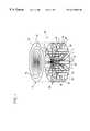
- FIG. 1is a partially exploded view of one embodiment of a high efficiency broadband antenna of the present invention.
- FIG. 2is an assembled view of the high efficiency broadband antenna of FIG. 1 shown with a cylindrical housing partially removed and a spiral winding.
- FIG. 3is a log-periodic structure for use in the high efficiency broadband antenna of the present invention.
- FIG. 4is a sinuous structure for use in the high efficiency broadband antenna of the present invention.
- a high efficiency broadband antenna 10constructed in accordance with the present invention, preferably comprises a unidirectional spiral antenna or spiral winding 12 .
- the high efficiency broadband antenna 10is the antenna of choice for ESM and ELINT systems.
- the spiral antenna 10is multi-octave in bandwidth, which offers a high probability of intercept.
- the spiral antenna 10also exhibits a wide beamwidth, which fulfills the field-of-view requirements of a wide-angle system.
- the unidirectional spiral antenna 10includes at least two planar conductors 14 , 16 , which are cooperatingly arranged in a substantially planar, bifilar spiral winding 12 .
- the two planar conductors 14 , 16may be wound in an equiangular or Archimedean spiral as is well known in the art.
- the planar conductors 14 , 16are etched on a thin copper clad KaptonTM or MylarTM material 18 , which is preferably approximately two mils in thickness.
- the high efficiency broadband antenna 10 of the present inventionalso includes a substantially frequency-independent reflective backing 20 situated on one axial side of the spiral winding 12 .
- the reflective backing 20includes a photonic crystal-like, quasi-periodic dielectric structure whose elements are scaled in radial dimension to the spiral winding of the planar conductors. Stated another way, the reflective backing 20 is formed as dielectric exhibiting propagation band-stop properties which scale in band-stop frequencies inversely with the radius of the spiral winding 12 .
- Photonic band-gap (PBG) materialsare analogous to a semiconductor crystal which has electron band gaps. Band gaps are energy levels which are not occupied by electrons.
- a PBG material or photonic crystalis an artificial material made of periodic implants within a surrounding medium. Electromagnetic wave propagation through such a medium is affected by the scattering and diffraction properties of the periodic implants creating frequency “stop bands” in which wave propagation is blocked.
- the photonic crystalas a substrate material for planar antennas, results in an antenna that radiates predominantly into the air rather than into the substrate.
- the quasi-periodic dielectric structure or reflective backing 20preferably includes a solid dielectric substrate 22 formed as a disk, which is situated on one side of the spiral winding 12 and, preferably, inside a cavity defined by the cylindrical housing 24 of the high efficiency broadband antenna 10 .
- the solid dielectric substrate 22has a predetermined dielectric constant, which is relatively high.
- the dielectric constant of the solid dielectric substrate 22is preferably about 10 and, even more preferably, even greater so that spacings in the periodic structure can both appear microscopic to the radiating element and yet be commensurate with the wavelength within the dielectric in order to enhance Bragg scattering within it.
- Aluminacomprising a dielectric constant near 10
- the solid dielectric substrate 22may be molded to the desired shape and dimensions.
- the reflective backing 20also includes three mutually perpendicular arrays of elongated dielectric elements.
- the dielectric elements of the arraysare at least partially embedded in the solid dielectric substrate 22 .
- the elongated dielectric elementsalso have a predetermined dielectric constant, which is relatively low, and which is preferably much less than that of the solid dielectric substrate to provide sufficient scattering. More specifically, the dielectric constant of the three elongated dielectric elements is preferably between about 1 and about 2. Also, with this lower dielectric constant, the elongated dielectric elements should be able to withstand relatively high temperatures if the composite backing material is formed by sintering.
- the first arrayincludes a plurality of first elongated dielectric elements in the form of rods 26 . These rods 26 are arranged in a plurality of planes extending substantially radially through the solid dielectric substrate 22 , outwardly from the center of the substrate 22 .
- the center of the solid dielectric substrate 22is preferably situated substantially co-axially with the center of the spiral winding 12 .
- Adjacent planes in which the rods 26 residediverge outwardly through the solid dielectric substrate 22 at a predetermined angle ⁇ . Stated differently, adjacent planes of rods 26 are offset from one another at angle ⁇ .
- the rods 26 of any respective planeare disposed substantially in parallel and spaced apart from one another in a side-by-side arrangement. Each rod 26 has a substantially constant diameter along its length. The diameter of the rods 26 and the spacing between adjacent rods 26 are at least approximately scaled with the radius of the spiral winding 12 . In other words, a more radially outwardly disposed rod 26 in any respective plane has a greater diameter than that of a more radially inwardly disposed rod 26 in the same respective plane.
- the spacing between more radially outwardly disposed adjacent pairs of rods 26 of any respective planeis greater than the spacing between more radially inwardly disposed adjacent pairs of rods 26 of the same respective plane.
- the spacing between rod A and rod Bis greater than the spacing between rod B and rod C, and so forth towards the center of the solid dielectric substrate 22 .
- the quasi-periodic dielectric reflective backing 20further includes a second array having a plurality of second elongated dielectric elements in the form of cones 28 .
- the cones 28are situated between adjacent planes of rods 26 of the first array.
- the cones 28extend radially through the solid dielectric substrate 22 , from the center of the solid dielectric substrate 22 to its circumference.
- the cones 28have a diameter which increases in a radially outward direction through the dielectric substrate 22 .
- the diameter of the cones 28is at least approximately scaled with the radius of the spiral winding 12 .
- One or more cones 28may be situated between adjacent planes of rods 26 of the second array. As shown in FIGS. 1 and 2, two cones are disposed in a sidewise, tiered arrangement axially through the solid dielectric substrate 22 to define upper and lower dielectric cones respectively residing in upper and lower planes extending radially through the solid dielectric substrate 22 and substantially orthogonally to the planes in which the dielectric rods 26 reside.
- the quasi-periodic dielectric backing 20further includes a third array having a plurality of third elongated dielectric elements in the form of rings 30 .
- the rings 30are arranged substantially concentrically to each other and reside in a plane extending through the solid dielectric substrate 22 .
- the plane in which the rings 20 resideis substantially orthogonal to the planes in which the dielectric rods 26 of the first array reside.
- Each ring 30has a substantially constant diameter along its elongated length. However, the diameter of the rings 30 and the spacing between adjacent rings 30 are at least approximately scaled with the radius of the spiral winding 12 . Stated differently, a more radially outwardly disposed ring 30 , such as ring D, has a greater diameter than that of a more radially inwardly disposed ring, for example, ring E. Also, the spacing between more radially outwardly disposed adjacent pairs of rings 30 , such as between rings D and E, is greater than the spacing between more radially inwardly disposed adjacent pairs of rings, such as rings F and G, as illustrated by FIG. 1 .
- the quasi-periodic dielectric backing 20includes upper and lower dielectric cones I, J respectively residing in upper and lower parallel planes, and the rings 30 are situated between the upper and lower cones. Any one concentric ring 30 is further preferably situated between a respective pair of adjacent dielectric rods 26 of each of the radially disposed planes in which the rods 26 reside.
- ring Dresides between the upper cones I and lower cones J, and passes between rods A and B as well as the other outermost pair of dielectric rods 26 embedded in the solid dielectric substrate 22 .
- Ring Ethe next innermost concentric ring, passes between the upper and lower cones 28 as well as between rods B and C and the other rods 26 in other planes in a similar radial disposition with respect to rods B and C.
- the radial scaling of the rods, cones and ringscauses the band-stop properties of the composite structure to radially scale (i.e., the stop frequency increases with radius).
- the composite structurewill exhibit a stop-band in the active region of the spiral winding 12 regardless of the operating frequency.
- the solid dielectric substrate 22is formed from a ceramic commonly used for dielectric resonators.
- a ceramiccommonly used for dielectric resonators.
- Such ceramicshave a high dielectric constant and exhibit low losses. These parameters remain substantially stable with temperature.
- the dielectric constantis preferably chosen to be relatively high so that spacings in the periodic structure appear microscopic to the radiating spiral winding of antenna 12 , yet are commensurate with the wavelength within the solid dielectric substrate 22 so that Bragg scattering is enhanced.
- Such ceramicsinclude, but are not limited to, alumina and S8500, as described previously.
- the elongated dielectric elements (i.e., the rods 26 , cones 28 and rings 30 ) of the three mutually perpendicular arraysare formed of a lower dielectric-constant material, as mentioned previously.
- the quasi-periodic dielectric backing 20is formed by adding the lower dielectric-constant rods 26 , cones 28 and rings 30 to the higher-dielectric constant solid dielectric substrate 22 structure during the green state, that is, before sintering.
- cast dielectric materialsmay also be used in the formation of the solid dielectric substrate 22 and the embedded rods 26 , cones 28 and rings 30 . Although cast dielectric materials have a higher loss than that of sintered ceramics, such materials facilitate the fabrication and evaluation process.
- the spiral winding 12is affixed to one axial side of the reflective backing by preferably bonding with an adhesive or the like.
- the winding 12may also be formed by etching it on copper clad KaptonTM or MylarTM material or their equivalent, and then bonding the etched material to an axial side of the reflective backing 20 .
- the high efficiency broadband antenna 10 of the present inventionprovides unidirectionality and frequency independence, as well as wide bandwidth and beamwidth found in conventional spiral antennas.
- the reflective backing 20provides the antenna 10 with forward radiation as opposed to backward reflection or absorption, and increases the gain by 3 dB over conventional spiral antennas having absorber backings.
- planar spiral windingmay be replaced with a planar log-periodic structure such as that shown in FIG. 3 and described in the following references, which are hereby incorporated by reference.
- spiral windingmay be replaced by a sinuous structure such as that shown in FIG. 4 and described in the following references, which are hereby incorporated by reference.
Landscapes
- Aerials With Secondary Devices (AREA)
Abstract
Description
Claims (22)
Priority Applications (2)
| Application Number | Priority Date | Filing Date | Title |
|---|---|---|---|
| US09/251,162US6219006B1 (en) | 1999-02-17 | 1999-02-17 | High efficiency broadband antenna |
| US09/832,628US6424317B2 (en) | 1999-02-17 | 2001-04-11 | High efficiency broadband antenna |
Applications Claiming Priority (1)
| Application Number | Priority Date | Filing Date | Title |
|---|---|---|---|
| US09/251,162US6219006B1 (en) | 1999-02-17 | 1999-02-17 | High efficiency broadband antenna |
Related Child Applications (1)
| Application Number | Title | Priority Date | Filing Date |
|---|---|---|---|
| US09/832,628ContinuationUS6424317B2 (en) | 1999-02-17 | 2001-04-11 | High efficiency broadband antenna |
Publications (1)
| Publication Number | Publication Date |
|---|---|
| US6219006B1true US6219006B1 (en) | 2001-04-17 |
Family
ID=22950754
Family Applications (2)
| Application Number | Title | Priority Date | Filing Date |
|---|---|---|---|
| US09/251,162Expired - LifetimeUS6219006B1 (en) | 1999-02-17 | 1999-02-17 | High efficiency broadband antenna |
| US09/832,628Expired - Fee RelatedUS6424317B2 (en) | 1999-02-17 | 2001-04-11 | High efficiency broadband antenna |
Family Applications After (1)
| Application Number | Title | Priority Date | Filing Date |
|---|---|---|---|
| US09/832,628Expired - Fee RelatedUS6424317B2 (en) | 1999-02-17 | 2001-04-11 | High efficiency broadband antenna |
Country Status (1)
| Country | Link |
|---|---|
| US (2) | US6219006B1 (en) |
Cited By (133)
| Publication number | Priority date | Publication date | Assignee | Title |
|---|---|---|---|---|
| US6424317B2 (en)* | 1999-02-17 | 2002-07-23 | Ail Systems, Inc. | High efficiency broadband antenna |
| US6525697B1 (en)* | 2001-07-11 | 2003-02-25 | Cisco Technology, Inc. | Archimedes spiral array antenna |
| US20030087606A1 (en)* | 2001-11-07 | 2003-05-08 | Dybdal Robert B. | Method of determining communication link quality employing beacon signals |
| US6731248B2 (en)* | 2002-06-27 | 2004-05-04 | Harris Corporation | High efficiency printed circuit array of log-periodic dipole arrays |
| US6734827B2 (en)* | 2002-06-27 | 2004-05-11 | Harris Corporation | High efficiency printed circuit LPDA |
| FR2922687A1 (en)* | 2007-10-23 | 2009-04-24 | Thales Sa | COMPACT BROADBAND ANTENNA. |
| WO2010132368A1 (en) | 2009-05-11 | 2010-11-18 | Colby Leigh E | Therapeutic tooth bud ablation |
| US20130012144A1 (en)* | 2011-07-05 | 2013-01-10 | Broadcom Corporation | Wireless communication device utilizing radiation-pattern and/or polarization coded modulation |
| EP2629367A1 (en)* | 2012-02-17 | 2013-08-21 | Elettronica S.p.A. | Ultra-wide-band low-profile sinuous slot antenna array |
| US20130249762A1 (en)* | 2010-10-01 | 2013-09-26 | Thales | Broadband antenna reflector for a circular-polarized planar wire antenna and method for producing said antenna reflector |
| US20130252560A1 (en)* | 2012-03-23 | 2013-09-26 | Broadcom Corporation | Antenna System with Spiral Antenna Sections and Applications Thereof |
| FR3017493A1 (en)* | 2014-02-07 | 2015-08-14 | Thales Sa | COMPACT WIRED ANTENNA WITH RESISTIVE PATTERNS |
| US9674711B2 (en) | 2013-11-06 | 2017-06-06 | At&T Intellectual Property I, L.P. | Surface-wave communications and methods thereof |
| US9685992B2 (en) | 2014-10-03 | 2017-06-20 | At&T Intellectual Property I, L.P. | Circuit panel network and methods thereof |
| US9705610B2 (en) | 2014-10-21 | 2017-07-11 | At&T Intellectual Property I, L.P. | Transmission device with impairment compensation and methods for use therewith |
| US9705561B2 (en) | 2015-04-24 | 2017-07-11 | At&T Intellectual Property I, L.P. | Directional coupling device and methods for use therewith |
| US9722318B2 (en) | 2015-07-14 | 2017-08-01 | At&T Intellectual Property I, L.P. | Method and apparatus for coupling an antenna to a device |
| US9729197B2 (en) | 2015-10-01 | 2017-08-08 | At&T Intellectual Property I, L.P. | Method and apparatus for communicating network management traffic over a network |
| US9735833B2 (en) | 2015-07-31 | 2017-08-15 | At&T Intellectual Property I, L.P. | Method and apparatus for communications management in a neighborhood network |
| US9742462B2 (en) | 2014-12-04 | 2017-08-22 | At&T Intellectual Property I, L.P. | Transmission medium and communication interfaces and methods for use therewith |
| US9742521B2 (en) | 2014-11-20 | 2017-08-22 | At&T Intellectual Property I, L.P. | Transmission device with mode division multiplexing and methods for use therewith |
| US9748626B2 (en) | 2015-05-14 | 2017-08-29 | At&T Intellectual Property I, L.P. | Plurality of cables having different cross-sectional shapes which are bundled together to form a transmission medium |
| US9749013B2 (en) | 2015-03-17 | 2017-08-29 | At&T Intellectual Property I, L.P. | Method and apparatus for reducing attenuation of electromagnetic waves guided by a transmission medium |
| US9749053B2 (en) | 2015-07-23 | 2017-08-29 | At&T Intellectual Property I, L.P. | Node device, repeater and methods for use therewith |
| US9769128B2 (en) | 2015-09-28 | 2017-09-19 | At&T Intellectual Property I, L.P. | Method and apparatus for encryption of communications over a network |
| US9768833B2 (en) | 2014-09-15 | 2017-09-19 | At&T Intellectual Property I, L.P. | Method and apparatus for sensing a condition in a transmission medium of electromagnetic waves |
| US9769020B2 (en) | 2014-10-21 | 2017-09-19 | At&T Intellectual Property I, L.P. | Method and apparatus for responding to events affecting communications in a communication network |
| US9780834B2 (en) | 2014-10-21 | 2017-10-03 | At&T Intellectual Property I, L.P. | Method and apparatus for transmitting electromagnetic waves |
| US9787412B2 (en) | 2015-06-25 | 2017-10-10 | At&T Intellectual Property I, L.P. | Methods and apparatus for inducing a fundamental wave mode on a transmission medium |
| US9793951B2 (en) | 2015-07-15 | 2017-10-17 | At&T Intellectual Property I, L.P. | Method and apparatus for launching a wave mode that mitigates interference |
| US9793955B2 (en) | 2015-04-24 | 2017-10-17 | At&T Intellectual Property I, Lp | Passive electrical coupling device and methods for use therewith |
| US9793954B2 (en) | 2015-04-28 | 2017-10-17 | At&T Intellectual Property I, L.P. | Magnetic coupling device and methods for use therewith |
| US9800327B2 (en) | 2014-11-20 | 2017-10-24 | At&T Intellectual Property I, L.P. | Apparatus for controlling operations of a communication device and methods thereof |
| US9820146B2 (en) | 2015-06-12 | 2017-11-14 | At&T Intellectual Property I, L.P. | Method and apparatus for authentication and identity management of communicating devices |
| US9838896B1 (en) | 2016-12-09 | 2017-12-05 | At&T Intellectual Property I, L.P. | Method and apparatus for assessing network coverage |
| US9838078B2 (en) | 2015-07-31 | 2017-12-05 | At&T Intellectual Property I, L.P. | Method and apparatus for exchanging communication signals |
| US9847850B2 (en) | 2014-10-14 | 2017-12-19 | At&T Intellectual Property I, L.P. | Method and apparatus for adjusting a mode of communication in a communication network |
| US9847566B2 (en) | 2015-07-14 | 2017-12-19 | At&T Intellectual Property I, L.P. | Method and apparatus for adjusting a field of a signal to mitigate interference |
| US9853342B2 (en) | 2015-07-14 | 2017-12-26 | At&T Intellectual Property I, L.P. | Dielectric transmission medium connector and methods for use therewith |
| US9860075B1 (en) | 2016-08-26 | 2018-01-02 | At&T Intellectual Property I, L.P. | Method and communication node for broadband distribution |
| US9865911B2 (en) | 2015-06-25 | 2018-01-09 | At&T Intellectual Property I, L.P. | Waveguide system for slot radiating first electromagnetic waves that are combined into a non-fundamental wave mode second electromagnetic wave on a transmission medium |
| US9866276B2 (en) | 2014-10-10 | 2018-01-09 | At&T Intellectual Property I, L.P. | Method and apparatus for arranging communication sessions in a communication system |
| US9866309B2 (en) | 2015-06-03 | 2018-01-09 | At&T Intellectual Property I, Lp | Host node device and methods for use therewith |
| US9871282B2 (en) | 2015-05-14 | 2018-01-16 | At&T Intellectual Property I, L.P. | At least one transmission medium having a dielectric surface that is covered at least in part by a second dielectric |
| US9871283B2 (en) | 2015-07-23 | 2018-01-16 | At&T Intellectual Property I, Lp | Transmission medium having a dielectric core comprised of plural members connected by a ball and socket configuration |
| US9871558B2 (en) | 2014-10-21 | 2018-01-16 | At&T Intellectual Property I, L.P. | Guided-wave transmission device and methods for use therewith |
| US9876605B1 (en) | 2016-10-21 | 2018-01-23 | At&T Intellectual Property I, L.P. | Launcher and coupling system to support desired guided wave mode |
| US9876264B2 (en) | 2015-10-02 | 2018-01-23 | At&T Intellectual Property I, Lp | Communication system, guided wave switch and methods for use therewith |
| US9876571B2 (en) | 2015-02-20 | 2018-01-23 | At&T Intellectual Property I, Lp | Guided-wave transmission device with non-fundamental mode propagation and methods for use therewith |
| US9882257B2 (en) | 2015-07-14 | 2018-01-30 | At&T Intellectual Property I, L.P. | Method and apparatus for launching a wave mode that mitigates interference |
| US9887447B2 (en) | 2015-05-14 | 2018-02-06 | At&T Intellectual Property I, L.P. | Transmission medium having multiple cores and methods for use therewith |
| US9893795B1 (en) | 2016-12-07 | 2018-02-13 | At&T Intellectual Property I, Lp | Method and repeater for broadband distribution |
| US9906269B2 (en) | 2014-09-17 | 2018-02-27 | At&T Intellectual Property I, L.P. | Monitoring and mitigating conditions in a communication network |
| US9904535B2 (en) | 2015-09-14 | 2018-02-27 | At&T Intellectual Property I, L.P. | Method and apparatus for distributing software |
| US9913139B2 (en) | 2015-06-09 | 2018-03-06 | At&T Intellectual Property I, L.P. | Signal fingerprinting for authentication of communicating devices |
| US9912381B2 (en) | 2015-06-03 | 2018-03-06 | At&T Intellectual Property I, Lp | Network termination and methods for use therewith |
| US9912033B2 (en) | 2014-10-21 | 2018-03-06 | At&T Intellectual Property I, Lp | Guided wave coupler, coupling module and methods for use therewith |
| US9912027B2 (en) | 2015-07-23 | 2018-03-06 | At&T Intellectual Property I, L.P. | Method and apparatus for exchanging communication signals |
| US9911020B1 (en) | 2016-12-08 | 2018-03-06 | At&T Intellectual Property I, L.P. | Method and apparatus for tracking via a radio frequency identification device |
| US9917341B2 (en) | 2015-05-27 | 2018-03-13 | At&T Intellectual Property I, L.P. | Apparatus and method for launching electromagnetic waves and for modifying radial dimensions of the propagating electromagnetic waves |
| US9927517B1 (en) | 2016-12-06 | 2018-03-27 | At&T Intellectual Property I, L.P. | Apparatus and methods for sensing rainfall |
| US9929755B2 (en) | 2015-07-14 | 2018-03-27 | At&T Intellectual Property I, L.P. | Method and apparatus for coupling an antenna to a device |
| US9948333B2 (en) | 2015-07-23 | 2018-04-17 | At&T Intellectual Property I, L.P. | Method and apparatus for wireless communications to mitigate interference |
| US9954287B2 (en) | 2014-11-20 | 2018-04-24 | At&T Intellectual Property I, L.P. | Apparatus for converting wireless signals and electromagnetic waves and methods thereof |
| US9954286B2 (en) | 2014-10-21 | 2018-04-24 | At&T Intellectual Property I, L.P. | Guided-wave transmission device with non-fundamental mode propagation and methods for use therewith |
| US9967173B2 (en) | 2015-07-31 | 2018-05-08 | At&T Intellectual Property I, L.P. | Method and apparatus for authentication and identity management of communicating devices |
| US9973940B1 (en) | 2017-02-27 | 2018-05-15 | At&T Intellectual Property I, L.P. | Apparatus and methods for dynamic impedance matching of a guided wave launcher |
| US9973416B2 (en) | 2014-10-02 | 2018-05-15 | At&T Intellectual Property I, L.P. | Method and apparatus that provides fault tolerance in a communication network |
| US9991580B2 (en) | 2016-10-21 | 2018-06-05 | At&T Intellectual Property I, L.P. | Launcher and coupling system for guided wave mode cancellation |
| US9998870B1 (en) | 2016-12-08 | 2018-06-12 | At&T Intellectual Property I, L.P. | Method and apparatus for proximity sensing |
| US9999038B2 (en) | 2013-05-31 | 2018-06-12 | At&T Intellectual Property I, L.P. | Remote distributed antenna system |
| US9997819B2 (en) | 2015-06-09 | 2018-06-12 | At&T Intellectual Property I, L.P. | Transmission medium and method for facilitating propagation of electromagnetic waves via a core |
| US10009067B2 (en) | 2014-12-04 | 2018-06-26 | At&T Intellectual Property I, L.P. | Method and apparatus for configuring a communication interface |
| US10020844B2 (en) | 2016-12-06 | 2018-07-10 | T&T Intellectual Property I, L.P. | Method and apparatus for broadcast communication via guided waves |
| US10027397B2 (en) | 2016-12-07 | 2018-07-17 | At&T Intellectual Property I, L.P. | Distributed antenna system and methods for use therewith |
| US10044409B2 (en) | 2015-07-14 | 2018-08-07 | At&T Intellectual Property I, L.P. | Transmission medium and methods for use therewith |
| US10051630B2 (en) | 2013-05-31 | 2018-08-14 | At&T Intellectual Property I, L.P. | Remote distributed antenna system |
| US10069185B2 (en) | 2015-06-25 | 2018-09-04 | At&T Intellectual Property I, L.P. | Methods and apparatus for inducing a non-fundamental wave mode on a transmission medium |
| US10069535B2 (en) | 2016-12-08 | 2018-09-04 | At&T Intellectual Property I, L.P. | Apparatus and methods for launching electromagnetic waves having a certain electric field structure |
| US10090606B2 (en) | 2015-07-15 | 2018-10-02 | At&T Intellectual Property I, L.P. | Antenna system with dielectric array and methods for use therewith |
| US10090594B2 (en) | 2016-11-23 | 2018-10-02 | At&T Intellectual Property I, L.P. | Antenna system having structural configurations for assembly |
| US10103422B2 (en) | 2016-12-08 | 2018-10-16 | At&T Intellectual Property I, L.P. | Method and apparatus for mounting network devices |
| US10135145B2 (en) | 2016-12-06 | 2018-11-20 | At&T Intellectual Property I, L.P. | Apparatus and methods for generating an electromagnetic wave along a transmission medium |
| US10135147B2 (en) | 2016-10-18 | 2018-11-20 | At&T Intellectual Property I, L.P. | Apparatus and methods for launching guided waves via an antenna |
| US10139820B2 (en) | 2016-12-07 | 2018-11-27 | At&T Intellectual Property I, L.P. | Method and apparatus for deploying equipment of a communication system |
| US10148016B2 (en) | 2015-07-14 | 2018-12-04 | At&T Intellectual Property I, L.P. | Apparatus and methods for communicating utilizing an antenna array |
| US10168695B2 (en) | 2016-12-07 | 2019-01-01 | At&T Intellectual Property I, L.P. | Method and apparatus for controlling an unmanned aircraft |
| US10178445B2 (en) | 2016-11-23 | 2019-01-08 | At&T Intellectual Property I, L.P. | Methods, devices, and systems for load balancing between a plurality of waveguides |
| US10205655B2 (en) | 2015-07-14 | 2019-02-12 | At&T Intellectual Property I, L.P. | Apparatus and methods for communicating utilizing an antenna array and multiple communication paths |
| US10225025B2 (en) | 2016-11-03 | 2019-03-05 | At&T Intellectual Property I, L.P. | Method and apparatus for detecting a fault in a communication system |
| US10224634B2 (en) | 2016-11-03 | 2019-03-05 | At&T Intellectual Property I, L.P. | Methods and apparatus for adjusting an operational characteristic of an antenna |
| US10243270B2 (en) | 2016-12-07 | 2019-03-26 | At&T Intellectual Property I, L.P. | Beam adaptive multi-feed dielectric antenna system and methods for use therewith |
| US10243784B2 (en) | 2014-11-20 | 2019-03-26 | At&T Intellectual Property I, L.P. | System for generating topology information and methods thereof |
| US10264586B2 (en) | 2016-12-09 | 2019-04-16 | At&T Mobility Ii Llc | Cloud-based packet controller and methods for use therewith |
| US10291334B2 (en) | 2016-11-03 | 2019-05-14 | At&T Intellectual Property I, L.P. | System for detecting a fault in a communication system |
| US10298293B2 (en) | 2017-03-13 | 2019-05-21 | At&T Intellectual Property I, L.P. | Apparatus of communication utilizing wireless network devices |
| US10305190B2 (en) | 2016-12-01 | 2019-05-28 | At&T Intellectual Property I, L.P. | Reflecting dielectric antenna system and methods for use therewith |
| US10312567B2 (en) | 2016-10-26 | 2019-06-04 | At&T Intellectual Property I, L.P. | Launcher with planar strip antenna and methods for use therewith |
| US10326494B2 (en) | 2016-12-06 | 2019-06-18 | At&T Intellectual Property I, L.P. | Apparatus for measurement de-embedding and methods for use therewith |
| US10326689B2 (en) | 2016-12-08 | 2019-06-18 | At&T Intellectual Property I, L.P. | Method and system for providing alternative communication paths |
| US10340573B2 (en) | 2016-10-26 | 2019-07-02 | At&T Intellectual Property I, L.P. | Launcher with cylindrical coupling device and methods for use therewith |
| US10340603B2 (en) | 2016-11-23 | 2019-07-02 | At&T Intellectual Property I, L.P. | Antenna system having shielded structural configurations for assembly |
| US10340601B2 (en) | 2016-11-23 | 2019-07-02 | At&T Intellectual Property I, L.P. | Multi-antenna system and methods for use therewith |
| US10340983B2 (en) | 2016-12-09 | 2019-07-02 | At&T Intellectual Property I, L.P. | Method and apparatus for surveying remote sites via guided wave communications |
| US10355367B2 (en) | 2015-10-16 | 2019-07-16 | At&T Intellectual Property I, L.P. | Antenna structure for exchanging wireless signals |
| US10359749B2 (en) | 2016-12-07 | 2019-07-23 | At&T Intellectual Property I, L.P. | Method and apparatus for utilities management via guided wave communication |
| US10361489B2 (en) | 2016-12-01 | 2019-07-23 | At&T Intellectual Property I, L.P. | Dielectric dish antenna system and methods for use therewith |
| US10374316B2 (en) | 2016-10-21 | 2019-08-06 | At&T Intellectual Property I, L.P. | System and dielectric antenna with non-uniform dielectric |
| US10382976B2 (en) | 2016-12-06 | 2019-08-13 | At&T Intellectual Property I, L.P. | Method and apparatus for managing wireless communications based on communication paths and network device positions |
| US10389037B2 (en) | 2016-12-08 | 2019-08-20 | At&T Intellectual Property I, L.P. | Apparatus and methods for selecting sections of an antenna array and use therewith |
| US10389029B2 (en) | 2016-12-07 | 2019-08-20 | At&T Intellectual Property I, L.P. | Multi-feed dielectric antenna system with core selection and methods for use therewith |
| US10411356B2 (en) | 2016-12-08 | 2019-09-10 | At&T Intellectual Property I, L.P. | Apparatus and methods for selectively targeting communication devices with an antenna array |
| US10439675B2 (en) | 2016-12-06 | 2019-10-08 | At&T Intellectual Property I, L.P. | Method and apparatus for repeating guided wave communication signals |
| US10446936B2 (en) | 2016-12-07 | 2019-10-15 | At&T Intellectual Property I, L.P. | Multi-feed dielectric antenna system and methods for use therewith |
| US10498044B2 (en) | 2016-11-03 | 2019-12-03 | At&T Intellectual Property I, L.P. | Apparatus for configuring a surface of an antenna |
| US10530505B2 (en) | 2016-12-08 | 2020-01-07 | At&T Intellectual Property I, L.P. | Apparatus and methods for launching electromagnetic waves along a transmission medium |
| US10535928B2 (en) | 2016-11-23 | 2020-01-14 | At&T Intellectual Property I, L.P. | Antenna system and methods for use therewith |
| US10547348B2 (en) | 2016-12-07 | 2020-01-28 | At&T Intellectual Property I, L.P. | Method and apparatus for switching transmission mediums in a communication system |
| US10601494B2 (en) | 2016-12-08 | 2020-03-24 | At&T Intellectual Property I, L.P. | Dual-band communication device and method for use therewith |
| US10637149B2 (en) | 2016-12-06 | 2020-04-28 | At&T Intellectual Property I, L.P. | Injection molded dielectric antenna and methods for use therewith |
| US10650940B2 (en) | 2015-05-15 | 2020-05-12 | At&T Intellectual Property I, L.P. | Transmission medium having a conductive material and methods for use therewith |
| US10694379B2 (en) | 2016-12-06 | 2020-06-23 | At&T Intellectual Property I, L.P. | Waveguide system with device-based authentication and methods for use therewith |
| US10727599B2 (en) | 2016-12-06 | 2020-07-28 | At&T Intellectual Property I, L.P. | Launcher with slot antenna and methods for use therewith |
| US10755542B2 (en) | 2016-12-06 | 2020-08-25 | At&T Intellectual Property I, L.P. | Method and apparatus for surveillance via guided wave communication |
| US10777873B2 (en) | 2016-12-08 | 2020-09-15 | At&T Intellectual Property I, L.P. | Method and apparatus for mounting network devices |
| US10797781B2 (en) | 2015-06-03 | 2020-10-06 | At&T Intellectual Property I, L.P. | Client node device and methods for use therewith |
| US10811767B2 (en) | 2016-10-21 | 2020-10-20 | At&T Intellectual Property I, L.P. | System and dielectric antenna with convex dielectric radome |
| US10819035B2 (en) | 2016-12-06 | 2020-10-27 | At&T Intellectual Property I, L.P. | Launcher with helical antenna and methods for use therewith |
| RU2737036C1 (en)* | 2019-12-31 | 2020-11-24 | Акционерное общество "Центральное конструкторское бюро автоматики" | Helical antenna |
| US10916969B2 (en) | 2016-12-08 | 2021-02-09 | At&T Intellectual Property I, L.P. | Method and apparatus for providing power using an inductive coupling |
| US10938108B2 (en) | 2016-12-08 | 2021-03-02 | At&T Intellectual Property I, L.P. | Frequency selective multi-feed dielectric antenna system and methods for use therewith |
| US11145987B2 (en)* | 2017-08-18 | 2021-10-12 | Xian Xiao S'antenna Technology Co., Ltd. | Ultralight artificial medium multilayer cylindrical lens |
| US11495886B2 (en)* | 2018-01-04 | 2022-11-08 | The Board Of Trustees Of The University Of Alabama | Cavity-backed spiral antenna with perturbation elements |
Families Citing this family (12)
| Publication number | Priority date | Publication date | Assignee | Title |
|---|---|---|---|---|
| GB0105251D0 (en) | 2001-03-02 | 2001-04-18 | Nokia Mobile Phones Ltd | Antenna |
| EP1239539A3 (en)* | 2001-03-02 | 2003-11-05 | Nokia Corporation | Antenna |
| US6759984B2 (en)* | 2001-06-01 | 2004-07-06 | Agere Systems Inc. | Low-loss printed circuit board antenna structure and method of manufacture thereof |
| US6677913B2 (en)* | 2001-06-19 | 2004-01-13 | The Regents Of The University Of California | Log-periodic antenna |
| US6842149B2 (en)* | 2003-01-24 | 2005-01-11 | Solectron Corporation | Combined mechanical package shield antenna |
| US7057560B2 (en) | 2003-05-07 | 2006-06-06 | Agere Systems Inc. | Dual-band antenna for a wireless local area network device |
| US6922179B2 (en)* | 2003-11-17 | 2005-07-26 | Winegard Company | Low profile television antenna |
| CN100463289C (en)* | 2006-03-24 | 2009-02-18 | 厦门大学 | Planar Helical Microstrip Antenna for 3G System Mobile Terminal |
| US7777689B2 (en) | 2006-12-06 | 2010-08-17 | Agere Systems Inc. | USB device, an attached protective cover therefore including an antenna and a method of wirelessly transmitting data |
| US7460083B2 (en)* | 2007-04-10 | 2008-12-02 | Harris Corporation | Antenna assembly and associated methods such as for receiving multiple signals |
| US8260201B2 (en)* | 2007-07-30 | 2012-09-04 | Bae Systems Information And Electronic Systems Integration Inc. | Dispersive antenna for RFID tags |
| US10644395B2 (en)* | 2018-05-14 | 2020-05-05 | Freefall Aerospace, Inc. | Dielectric antenna array and system |
Citations (5)
| Publication number | Priority date | Publication date | Assignee | Title |
|---|---|---|---|---|
| US4658262A (en) | 1985-02-19 | 1987-04-14 | Duhamel Raymond H | Dual polarized sinuous antennas |
| US5386215A (en) | 1992-11-20 | 1995-01-31 | Massachusetts Institute Of Technology | Highly efficient planar antenna on a periodic dielectric structure |
| US5541613A (en) | 1994-11-03 | 1996-07-30 | Hughes Aircraft Company, Hughes Electronics | Efficient broadband antenna system using photonic bandgap crystals |
| US5739796A (en) | 1995-10-30 | 1998-04-14 | The United States Of America As Represented By The Secretary Of The Army | Ultra-wideband photonic band gap crystal having selectable and controllable bad gaps and methods for achieving photonic band gaps |
| US5990850A (en)* | 1995-03-17 | 1999-11-23 | Massachusetts Institute Of Technology | Metallodielectric photonic crystal |
Family Cites Families (1)
| Publication number | Priority date | Publication date | Assignee | Title |
|---|---|---|---|---|
| US6219006B1 (en)* | 1999-02-17 | 2001-04-17 | Ail Systems, Inc. | High efficiency broadband antenna |
- 1999
- 1999-02-17USUS09/251,162patent/US6219006B1/ennot_activeExpired - Lifetime
- 2001
- 2001-04-11USUS09/832,628patent/US6424317B2/ennot_activeExpired - Fee Related
Patent Citations (5)
| Publication number | Priority date | Publication date | Assignee | Title |
|---|---|---|---|---|
| US4658262A (en) | 1985-02-19 | 1987-04-14 | Duhamel Raymond H | Dual polarized sinuous antennas |
| US5386215A (en) | 1992-11-20 | 1995-01-31 | Massachusetts Institute Of Technology | Highly efficient planar antenna on a periodic dielectric structure |
| US5541613A (en) | 1994-11-03 | 1996-07-30 | Hughes Aircraft Company, Hughes Electronics | Efficient broadband antenna system using photonic bandgap crystals |
| US5990850A (en)* | 1995-03-17 | 1999-11-23 | Massachusetts Institute Of Technology | Metallodielectric photonic crystal |
| US5739796A (en) | 1995-10-30 | 1998-04-14 | The United States Of America As Represented By The Secretary Of The Army | Ultra-wideband photonic band gap crystal having selectable and controllable bad gaps and methods for achieving photonic band gaps |
Non-Patent Citations (11)
| Title |
|---|
| D. A. Hofer, Dr. O.B. Kesler and L.L. Lovet, A Compact Multi-Polarized Broadband Antenna, IEEE Antennas & Propagation Symposium Digest, vol. 1, pp. 522-525 (1990). |
| E. R. Brown, C.D. Parker, E. Yablonovitch, Radiation Properties of a Planar Antenna on a Photonic-Crystal Subtrate, J. Opt. Soc. Am. B., vol. 10, No. 2 (Feb. 1993). |
| E. Yablonovitch, Inhibited Spontaneous Emission in Solid-State Physics and Electronics, Physical Review Letters-The American Physical Society, vol. 58, No. 20 (May 18, 1987). |
| E. Yablonovitch, Inhibited Spontaneous Emission in Solid-State Physics and Electronics, Physical Review Letters—The American Physical Society, vol. 58, No. 20 (May 18, 1987). |
| E. Yablonovitch, T.J. Gmitter, K.M. Leung, Photonic Band Structure: The Face Centered-Cubic Case Employing Non-Spherical Atoms, Physical Review Letters-The American Physical Society, vol. 67, No. 17 (Oct. 21, 1991). |
| E. Yablonovitch, T.J. Gmitter, K.M. Leung, Photonic Band Structure: The Face Centered-Cubic Case Employing Non-Spherical Atoms, Physical Review Letters—The American Physical Society, vol. 67, No. 17 (Oct. 21, 1991). |
| E. Yablonovitch, T.J. Gmitter, Photonic Band Structure: The Force-Centered Cube Case, J. Opt. Soc. Am. B., vol. 7, No. 9 (Sep. 1990). |
| H. Y. D. Yang, N.G. Alexopoulos, E. Yablonovitch, Photonic Band-Gap Materials for High Gain Printed Circuit Antennas, IEEE Transactions on Antennas and Propagation, vol. 45, No. 1 (Jan. 1997). |
| P. Asbeck, J. Mink, T. Itoh and G. Haddad, Device and Circuit Approaches for Next-Generation Wireless Communications, Microwave Journal, pp. 28-42 (1999). |
| R. E. Franks C.T. Elfving, Reflector-Type Periodic Broadband Antennas, 1958 IRE WESCON Convention Record, pp. 266-271. |
| V. K. Tripp and J. J. H. Wang, The Sinuous Microstrip Antenna, IEEE Antennas & Propagation Symposium Digest, vol. 1, pp. 52-55 (1991). |
Cited By (149)
| Publication number | Priority date | Publication date | Assignee | Title |
|---|---|---|---|---|
| US6424317B2 (en)* | 1999-02-17 | 2002-07-23 | Ail Systems, Inc. | High efficiency broadband antenna |
| US6525697B1 (en)* | 2001-07-11 | 2003-02-25 | Cisco Technology, Inc. | Archimedes spiral array antenna |
| US20030087606A1 (en)* | 2001-11-07 | 2003-05-08 | Dybdal Robert B. | Method of determining communication link quality employing beacon signals |
| US7373105B2 (en)* | 2001-11-07 | 2008-05-13 | The Aerospace Corporation | Method of determining communication link quality employing beacon signals |
| US6731248B2 (en)* | 2002-06-27 | 2004-05-04 | Harris Corporation | High efficiency printed circuit array of log-periodic dipole arrays |
| US6734827B2 (en)* | 2002-06-27 | 2004-05-11 | Harris Corporation | High efficiency printed circuit LPDA |
| FR2922687A1 (en)* | 2007-10-23 | 2009-04-24 | Thales Sa | COMPACT BROADBAND ANTENNA. |
| WO2010132368A1 (en) | 2009-05-11 | 2010-11-18 | Colby Leigh E | Therapeutic tooth bud ablation |
| US20130249762A1 (en)* | 2010-10-01 | 2013-09-26 | Thales | Broadband antenna reflector for a circular-polarized planar wire antenna and method for producing said antenna reflector |
| US9755317B2 (en)* | 2010-10-01 | 2017-09-05 | Thales | Broadband antenna reflector for a circular-polarized planar wire antenna and method for producing said antenna reflector |
| US20130012144A1 (en)* | 2011-07-05 | 2013-01-10 | Broadcom Corporation | Wireless communication device utilizing radiation-pattern and/or polarization coded modulation |
| EP2629367A1 (en)* | 2012-02-17 | 2013-08-21 | Elettronica S.p.A. | Ultra-wide-band low-profile sinuous slot antenna array |
| US20130252560A1 (en)* | 2012-03-23 | 2013-09-26 | Broadcom Corporation | Antenna System with Spiral Antenna Sections and Applications Thereof |
| US9999038B2 (en) | 2013-05-31 | 2018-06-12 | At&T Intellectual Property I, L.P. | Remote distributed antenna system |
| US10051630B2 (en) | 2013-05-31 | 2018-08-14 | At&T Intellectual Property I, L.P. | Remote distributed antenna system |
| US9674711B2 (en) | 2013-11-06 | 2017-06-06 | At&T Intellectual Property I, L.P. | Surface-wave communications and methods thereof |
| FR3017493A1 (en)* | 2014-02-07 | 2015-08-14 | Thales Sa | COMPACT WIRED ANTENNA WITH RESISTIVE PATTERNS |
| US9768833B2 (en) | 2014-09-15 | 2017-09-19 | At&T Intellectual Property I, L.P. | Method and apparatus for sensing a condition in a transmission medium of electromagnetic waves |
| US9906269B2 (en) | 2014-09-17 | 2018-02-27 | At&T Intellectual Property I, L.P. | Monitoring and mitigating conditions in a communication network |
| US10063280B2 (en) | 2014-09-17 | 2018-08-28 | At&T Intellectual Property I, L.P. | Monitoring and mitigating conditions in a communication network |
| US9973416B2 (en) | 2014-10-02 | 2018-05-15 | At&T Intellectual Property I, L.P. | Method and apparatus that provides fault tolerance in a communication network |
| US9685992B2 (en) | 2014-10-03 | 2017-06-20 | At&T Intellectual Property I, L.P. | Circuit panel network and methods thereof |
| US9866276B2 (en) | 2014-10-10 | 2018-01-09 | At&T Intellectual Property I, L.P. | Method and apparatus for arranging communication sessions in a communication system |
| US9847850B2 (en) | 2014-10-14 | 2017-12-19 | At&T Intellectual Property I, L.P. | Method and apparatus for adjusting a mode of communication in a communication network |
| US9769020B2 (en) | 2014-10-21 | 2017-09-19 | At&T Intellectual Property I, L.P. | Method and apparatus for responding to events affecting communications in a communication network |
| US9912033B2 (en) | 2014-10-21 | 2018-03-06 | At&T Intellectual Property I, Lp | Guided wave coupler, coupling module and methods for use therewith |
| US9871558B2 (en) | 2014-10-21 | 2018-01-16 | At&T Intellectual Property I, L.P. | Guided-wave transmission device and methods for use therewith |
| US9954286B2 (en) | 2014-10-21 | 2018-04-24 | At&T Intellectual Property I, L.P. | Guided-wave transmission device with non-fundamental mode propagation and methods for use therewith |
| US9876587B2 (en) | 2014-10-21 | 2018-01-23 | At&T Intellectual Property I, L.P. | Transmission device with impairment compensation and methods for use therewith |
| US9705610B2 (en) | 2014-10-21 | 2017-07-11 | At&T Intellectual Property I, L.P. | Transmission device with impairment compensation and methods for use therewith |
| US9780834B2 (en) | 2014-10-21 | 2017-10-03 | At&T Intellectual Property I, L.P. | Method and apparatus for transmitting electromagnetic waves |
| US9960808B2 (en) | 2014-10-21 | 2018-05-01 | At&T Intellectual Property I, L.P. | Guided-wave transmission device and methods for use therewith |
| US10243784B2 (en) | 2014-11-20 | 2019-03-26 | At&T Intellectual Property I, L.P. | System for generating topology information and methods thereof |
| US9749083B2 (en) | 2014-11-20 | 2017-08-29 | At&T Intellectual Property I, L.P. | Transmission device with mode division multiplexing and methods for use therewith |
| US9954287B2 (en) | 2014-11-20 | 2018-04-24 | At&T Intellectual Property I, L.P. | Apparatus for converting wireless signals and electromagnetic waves and methods thereof |
| US9800327B2 (en) | 2014-11-20 | 2017-10-24 | At&T Intellectual Property I, L.P. | Apparatus for controlling operations of a communication device and methods thereof |
| US9742521B2 (en) | 2014-11-20 | 2017-08-22 | At&T Intellectual Property I, L.P. | Transmission device with mode division multiplexing and methods for use therewith |
| US9742462B2 (en) | 2014-12-04 | 2017-08-22 | At&T Intellectual Property I, L.P. | Transmission medium and communication interfaces and methods for use therewith |
| US10009067B2 (en) | 2014-12-04 | 2018-06-26 | At&T Intellectual Property I, L.P. | Method and apparatus for configuring a communication interface |
| US9876571B2 (en) | 2015-02-20 | 2018-01-23 | At&T Intellectual Property I, Lp | Guided-wave transmission device with non-fundamental mode propagation and methods for use therewith |
| US9876570B2 (en) | 2015-02-20 | 2018-01-23 | At&T Intellectual Property I, Lp | Guided-wave transmission device with non-fundamental mode propagation and methods for use therewith |
| US9749013B2 (en) | 2015-03-17 | 2017-08-29 | At&T Intellectual Property I, L.P. | Method and apparatus for reducing attenuation of electromagnetic waves guided by a transmission medium |
| US9831912B2 (en) | 2015-04-24 | 2017-11-28 | At&T Intellectual Property I, Lp | Directional coupling device and methods for use therewith |
| US10224981B2 (en) | 2015-04-24 | 2019-03-05 | At&T Intellectual Property I, Lp | Passive electrical coupling device and methods for use therewith |
| US9793955B2 (en) | 2015-04-24 | 2017-10-17 | At&T Intellectual Property I, Lp | Passive electrical coupling device and methods for use therewith |
| US9705561B2 (en) | 2015-04-24 | 2017-07-11 | At&T Intellectual Property I, L.P. | Directional coupling device and methods for use therewith |
| US9793954B2 (en) | 2015-04-28 | 2017-10-17 | At&T Intellectual Property I, L.P. | Magnetic coupling device and methods for use therewith |
| US9748626B2 (en) | 2015-05-14 | 2017-08-29 | At&T Intellectual Property I, L.P. | Plurality of cables having different cross-sectional shapes which are bundled together to form a transmission medium |
| US9871282B2 (en) | 2015-05-14 | 2018-01-16 | At&T Intellectual Property I, L.P. | At least one transmission medium having a dielectric surface that is covered at least in part by a second dielectric |
| US9887447B2 (en) | 2015-05-14 | 2018-02-06 | At&T Intellectual Property I, L.P. | Transmission medium having multiple cores and methods for use therewith |
| US10650940B2 (en) | 2015-05-15 | 2020-05-12 | At&T Intellectual Property I, L.P. | Transmission medium having a conductive material and methods for use therewith |
| US9917341B2 (en) | 2015-05-27 | 2018-03-13 | At&T Intellectual Property I, L.P. | Apparatus and method for launching electromagnetic waves and for modifying radial dimensions of the propagating electromagnetic waves |
| US10812174B2 (en) | 2015-06-03 | 2020-10-20 | At&T Intellectual Property I, L.P. | Client node device and methods for use therewith |
| US9935703B2 (en) | 2015-06-03 | 2018-04-03 | At&T Intellectual Property I, L.P. | Host node device and methods for use therewith |
| US9866309B2 (en) | 2015-06-03 | 2018-01-09 | At&T Intellectual Property I, Lp | Host node device and methods for use therewith |
| US9967002B2 (en) | 2015-06-03 | 2018-05-08 | At&T Intellectual I, Lp | Network termination and methods for use therewith |
| US10797781B2 (en) | 2015-06-03 | 2020-10-06 | At&T Intellectual Property I, L.P. | Client node device and methods for use therewith |
| US10050697B2 (en) | 2015-06-03 | 2018-08-14 | At&T Intellectual Property I, L.P. | Host node device and methods for use therewith |
| US9912381B2 (en) | 2015-06-03 | 2018-03-06 | At&T Intellectual Property I, Lp | Network termination and methods for use therewith |
| US9912382B2 (en) | 2015-06-03 | 2018-03-06 | At&T Intellectual Property I, Lp | Network termination and methods for use therewith |
| US9997819B2 (en) | 2015-06-09 | 2018-06-12 | At&T Intellectual Property I, L.P. | Transmission medium and method for facilitating propagation of electromagnetic waves via a core |
| US9913139B2 (en) | 2015-06-09 | 2018-03-06 | At&T Intellectual Property I, L.P. | Signal fingerprinting for authentication of communicating devices |
| US9820146B2 (en) | 2015-06-12 | 2017-11-14 | At&T Intellectual Property I, L.P. | Method and apparatus for authentication and identity management of communicating devices |
| US9865911B2 (en) | 2015-06-25 | 2018-01-09 | At&T Intellectual Property I, L.P. | Waveguide system for slot radiating first electromagnetic waves that are combined into a non-fundamental wave mode second electromagnetic wave on a transmission medium |
| US10069185B2 (en) | 2015-06-25 | 2018-09-04 | At&T Intellectual Property I, L.P. | Methods and apparatus for inducing a non-fundamental wave mode on a transmission medium |
| US9787412B2 (en) | 2015-06-25 | 2017-10-10 | At&T Intellectual Property I, L.P. | Methods and apparatus for inducing a fundamental wave mode on a transmission medium |
| US10205655B2 (en) | 2015-07-14 | 2019-02-12 | At&T Intellectual Property I, L.P. | Apparatus and methods for communicating utilizing an antenna array and multiple communication paths |
| US10148016B2 (en) | 2015-07-14 | 2018-12-04 | At&T Intellectual Property I, L.P. | Apparatus and methods for communicating utilizing an antenna array |
| US9882257B2 (en) | 2015-07-14 | 2018-01-30 | At&T Intellectual Property I, L.P. | Method and apparatus for launching a wave mode that mitigates interference |
| US9929755B2 (en) | 2015-07-14 | 2018-03-27 | At&T Intellectual Property I, L.P. | Method and apparatus for coupling an antenna to a device |
| US10044409B2 (en) | 2015-07-14 | 2018-08-07 | At&T Intellectual Property I, L.P. | Transmission medium and methods for use therewith |
| US9847566B2 (en) | 2015-07-14 | 2017-12-19 | At&T Intellectual Property I, L.P. | Method and apparatus for adjusting a field of a signal to mitigate interference |
| US9853342B2 (en) | 2015-07-14 | 2017-12-26 | At&T Intellectual Property I, L.P. | Dielectric transmission medium connector and methods for use therewith |
| US9722318B2 (en) | 2015-07-14 | 2017-08-01 | At&T Intellectual Property I, L.P. | Method and apparatus for coupling an antenna to a device |
| US10090606B2 (en) | 2015-07-15 | 2018-10-02 | At&T Intellectual Property I, L.P. | Antenna system with dielectric array and methods for use therewith |
| US9793951B2 (en) | 2015-07-15 | 2017-10-17 | At&T Intellectual Property I, L.P. | Method and apparatus for launching a wave mode that mitigates interference |
| US9806818B2 (en) | 2015-07-23 | 2017-10-31 | At&T Intellectual Property I, Lp | Node device, repeater and methods for use therewith |
| US9871283B2 (en) | 2015-07-23 | 2018-01-16 | At&T Intellectual Property I, Lp | Transmission medium having a dielectric core comprised of plural members connected by a ball and socket configuration |
| US9749053B2 (en) | 2015-07-23 | 2017-08-29 | At&T Intellectual Property I, L.P. | Node device, repeater and methods for use therewith |
| US9948333B2 (en) | 2015-07-23 | 2018-04-17 | At&T Intellectual Property I, L.P. | Method and apparatus for wireless communications to mitigate interference |
| US9912027B2 (en) | 2015-07-23 | 2018-03-06 | At&T Intellectual Property I, L.P. | Method and apparatus for exchanging communication signals |
| US9967173B2 (en) | 2015-07-31 | 2018-05-08 | At&T Intellectual Property I, L.P. | Method and apparatus for authentication and identity management of communicating devices |
| US9838078B2 (en) | 2015-07-31 | 2017-12-05 | At&T Intellectual Property I, L.P. | Method and apparatus for exchanging communication signals |
| US9735833B2 (en) | 2015-07-31 | 2017-08-15 | At&T Intellectual Property I, L.P. | Method and apparatus for communications management in a neighborhood network |
| US9904535B2 (en) | 2015-09-14 | 2018-02-27 | At&T Intellectual Property I, L.P. | Method and apparatus for distributing software |
| US9769128B2 (en) | 2015-09-28 | 2017-09-19 | At&T Intellectual Property I, L.P. | Method and apparatus for encryption of communications over a network |
| US9729197B2 (en) | 2015-10-01 | 2017-08-08 | At&T Intellectual Property I, L.P. | Method and apparatus for communicating network management traffic over a network |
| US9876264B2 (en) | 2015-10-02 | 2018-01-23 | At&T Intellectual Property I, Lp | Communication system, guided wave switch and methods for use therewith |
| US10355367B2 (en) | 2015-10-16 | 2019-07-16 | At&T Intellectual Property I, L.P. | Antenna structure for exchanging wireless signals |
| US9860075B1 (en) | 2016-08-26 | 2018-01-02 | At&T Intellectual Property I, L.P. | Method and communication node for broadband distribution |
| US10135147B2 (en) | 2016-10-18 | 2018-11-20 | At&T Intellectual Property I, L.P. | Apparatus and methods for launching guided waves via an antenna |
| US10811767B2 (en) | 2016-10-21 | 2020-10-20 | At&T Intellectual Property I, L.P. | System and dielectric antenna with convex dielectric radome |
| US10374316B2 (en) | 2016-10-21 | 2019-08-06 | At&T Intellectual Property I, L.P. | System and dielectric antenna with non-uniform dielectric |
| US9876605B1 (en) | 2016-10-21 | 2018-01-23 | At&T Intellectual Property I, L.P. | Launcher and coupling system to support desired guided wave mode |
| US9991580B2 (en) | 2016-10-21 | 2018-06-05 | At&T Intellectual Property I, L.P. | Launcher and coupling system for guided wave mode cancellation |
| US10340573B2 (en) | 2016-10-26 | 2019-07-02 | At&T Intellectual Property I, L.P. | Launcher with cylindrical coupling device and methods for use therewith |
| US10312567B2 (en) | 2016-10-26 | 2019-06-04 | At&T Intellectual Property I, L.P. | Launcher with planar strip antenna and methods for use therewith |
| US10225025B2 (en) | 2016-11-03 | 2019-03-05 | At&T Intellectual Property I, L.P. | Method and apparatus for detecting a fault in a communication system |
| US10291334B2 (en) | 2016-11-03 | 2019-05-14 | At&T Intellectual Property I, L.P. | System for detecting a fault in a communication system |
| US10224634B2 (en) | 2016-11-03 | 2019-03-05 | At&T Intellectual Property I, L.P. | Methods and apparatus for adjusting an operational characteristic of an antenna |
| US10498044B2 (en) | 2016-11-03 | 2019-12-03 | At&T Intellectual Property I, L.P. | Apparatus for configuring a surface of an antenna |
| US10340603B2 (en) | 2016-11-23 | 2019-07-02 | At&T Intellectual Property I, L.P. | Antenna system having shielded structural configurations for assembly |
| US10340601B2 (en) | 2016-11-23 | 2019-07-02 | At&T Intellectual Property I, L.P. | Multi-antenna system and methods for use therewith |
| US10178445B2 (en) | 2016-11-23 | 2019-01-08 | At&T Intellectual Property I, L.P. | Methods, devices, and systems for load balancing between a plurality of waveguides |
| US10090594B2 (en) | 2016-11-23 | 2018-10-02 | At&T Intellectual Property I, L.P. | Antenna system having structural configurations for assembly |
| US10535928B2 (en) | 2016-11-23 | 2020-01-14 | At&T Intellectual Property I, L.P. | Antenna system and methods for use therewith |
| US10305190B2 (en) | 2016-12-01 | 2019-05-28 | At&T Intellectual Property I, L.P. | Reflecting dielectric antenna system and methods for use therewith |
| US10361489B2 (en) | 2016-12-01 | 2019-07-23 | At&T Intellectual Property I, L.P. | Dielectric dish antenna system and methods for use therewith |
| US10135145B2 (en) | 2016-12-06 | 2018-11-20 | At&T Intellectual Property I, L.P. | Apparatus and methods for generating an electromagnetic wave along a transmission medium |
| US10439675B2 (en) | 2016-12-06 | 2019-10-08 | At&T Intellectual Property I, L.P. | Method and apparatus for repeating guided wave communication signals |
| US10819035B2 (en) | 2016-12-06 | 2020-10-27 | At&T Intellectual Property I, L.P. | Launcher with helical antenna and methods for use therewith |
| US10637149B2 (en) | 2016-12-06 | 2020-04-28 | At&T Intellectual Property I, L.P. | Injection molded dielectric antenna and methods for use therewith |
| US10326494B2 (en) | 2016-12-06 | 2019-06-18 | At&T Intellectual Property I, L.P. | Apparatus for measurement de-embedding and methods for use therewith |
| US10382976B2 (en) | 2016-12-06 | 2019-08-13 | At&T Intellectual Property I, L.P. | Method and apparatus for managing wireless communications based on communication paths and network device positions |
| US10755542B2 (en) | 2016-12-06 | 2020-08-25 | At&T Intellectual Property I, L.P. | Method and apparatus for surveillance via guided wave communication |
| US10020844B2 (en) | 2016-12-06 | 2018-07-10 | T&T Intellectual Property I, L.P. | Method and apparatus for broadcast communication via guided waves |
| US10694379B2 (en) | 2016-12-06 | 2020-06-23 | At&T Intellectual Property I, L.P. | Waveguide system with device-based authentication and methods for use therewith |
| US10727599B2 (en) | 2016-12-06 | 2020-07-28 | At&T Intellectual Property I, L.P. | Launcher with slot antenna and methods for use therewith |
| US9927517B1 (en) | 2016-12-06 | 2018-03-27 | At&T Intellectual Property I, L.P. | Apparatus and methods for sensing rainfall |
| US10027397B2 (en) | 2016-12-07 | 2018-07-17 | At&T Intellectual Property I, L.P. | Distributed antenna system and methods for use therewith |
| US10139820B2 (en) | 2016-12-07 | 2018-11-27 | At&T Intellectual Property I, L.P. | Method and apparatus for deploying equipment of a communication system |
| US9893795B1 (en) | 2016-12-07 | 2018-02-13 | At&T Intellectual Property I, Lp | Method and repeater for broadband distribution |
| US10359749B2 (en) | 2016-12-07 | 2019-07-23 | At&T Intellectual Property I, L.P. | Method and apparatus for utilities management via guided wave communication |
| US10168695B2 (en) | 2016-12-07 | 2019-01-01 | At&T Intellectual Property I, L.P. | Method and apparatus for controlling an unmanned aircraft |
| US10389029B2 (en) | 2016-12-07 | 2019-08-20 | At&T Intellectual Property I, L.P. | Multi-feed dielectric antenna system with core selection and methods for use therewith |
| US10547348B2 (en) | 2016-12-07 | 2020-01-28 | At&T Intellectual Property I, L.P. | Method and apparatus for switching transmission mediums in a communication system |
| US10243270B2 (en) | 2016-12-07 | 2019-03-26 | At&T Intellectual Property I, L.P. | Beam adaptive multi-feed dielectric antenna system and methods for use therewith |
| US10446936B2 (en) | 2016-12-07 | 2019-10-15 | At&T Intellectual Property I, L.P. | Multi-feed dielectric antenna system and methods for use therewith |
| US10777873B2 (en) | 2016-12-08 | 2020-09-15 | At&T Intellectual Property I, L.P. | Method and apparatus for mounting network devices |
| US9998870B1 (en) | 2016-12-08 | 2018-06-12 | At&T Intellectual Property I, L.P. | Method and apparatus for proximity sensing |
| US10938108B2 (en) | 2016-12-08 | 2021-03-02 | At&T Intellectual Property I, L.P. | Frequency selective multi-feed dielectric antenna system and methods for use therewith |
| US10411356B2 (en) | 2016-12-08 | 2019-09-10 | At&T Intellectual Property I, L.P. | Apparatus and methods for selectively targeting communication devices with an antenna array |
| US10601494B2 (en) | 2016-12-08 | 2020-03-24 | At&T Intellectual Property I, L.P. | Dual-band communication device and method for use therewith |
| US10389037B2 (en) | 2016-12-08 | 2019-08-20 | At&T Intellectual Property I, L.P. | Apparatus and methods for selecting sections of an antenna array and use therewith |
| US10326689B2 (en) | 2016-12-08 | 2019-06-18 | At&T Intellectual Property I, L.P. | Method and system for providing alternative communication paths |
| US10103422B2 (en) | 2016-12-08 | 2018-10-16 | At&T Intellectual Property I, L.P. | Method and apparatus for mounting network devices |
| US10069535B2 (en) | 2016-12-08 | 2018-09-04 | At&T Intellectual Property I, L.P. | Apparatus and methods for launching electromagnetic waves having a certain electric field structure |
| US10916969B2 (en) | 2016-12-08 | 2021-02-09 | At&T Intellectual Property I, L.P. | Method and apparatus for providing power using an inductive coupling |
| US10530505B2 (en) | 2016-12-08 | 2020-01-07 | At&T Intellectual Property I, L.P. | Apparatus and methods for launching electromagnetic waves along a transmission medium |
| US10819034B2 (en) | 2016-12-08 | 2020-10-27 | At&T Intellectual Property I, L.P. | Apparatus and methods for selectively targeting communication devices with an antenna array |
| US9911020B1 (en) | 2016-12-08 | 2018-03-06 | At&T Intellectual Property I, L.P. | Method and apparatus for tracking via a radio frequency identification device |
| US10264586B2 (en) | 2016-12-09 | 2019-04-16 | At&T Mobility Ii Llc | Cloud-based packet controller and methods for use therewith |
| US10340983B2 (en) | 2016-12-09 | 2019-07-02 | At&T Intellectual Property I, L.P. | Method and apparatus for surveying remote sites via guided wave communications |
| US9838896B1 (en) | 2016-12-09 | 2017-12-05 | At&T Intellectual Property I, L.P. | Method and apparatus for assessing network coverage |
| US9973940B1 (en) | 2017-02-27 | 2018-05-15 | At&T Intellectual Property I, L.P. | Apparatus and methods for dynamic impedance matching of a guided wave launcher |
| US10298293B2 (en) | 2017-03-13 | 2019-05-21 | At&T Intellectual Property I, L.P. | Apparatus of communication utilizing wireless network devices |
| US11145987B2 (en)* | 2017-08-18 | 2021-10-12 | Xian Xiao S'antenna Technology Co., Ltd. | Ultralight artificial medium multilayer cylindrical lens |
| US11495886B2 (en)* | 2018-01-04 | 2022-11-08 | The Board Of Trustees Of The University Of Alabama | Cavity-backed spiral antenna with perturbation elements |
| RU2737036C1 (en)* | 2019-12-31 | 2020-11-24 | Акционерное общество "Центральное конструкторское бюро автоматики" | Helical antenna |
Also Published As
| Publication number | Publication date |
|---|---|
| US20010033251A1 (en) | 2001-10-25 |
| US6424317B2 (en) | 2002-07-23 |
Similar Documents
| Publication | Publication Date | Title |
|---|---|---|
| US6219006B1 (en) | High efficiency broadband antenna | |
| Qian et al. | A novel approach for gain and bandwidth enhancement of patch antennas | |
| US5541613A (en) | Efficient broadband antenna system using photonic bandgap crystals | |
| Ouedraogo et al. | Miniaturization of patch antennas using a metamaterial-inspired technique | |
| KR0148253B1 (en) | Flush Surface Wave Antenna | |
| US5689275A (en) | Electromagnetic antenna and transmission line utilizing photonic bandgap material | |
| US5589842A (en) | Compact microstrip antenna with magnetic substrate | |
| Yang et al. | A novel surface‐wave antenna design using a thin periodically loaded ground plane | |
| CN110199436B (en) | Multi-band circularly polarized antenna | |
| US6919854B2 (en) | Variable inclination continuous transverse stub array | |
| GB2175748A (en) | Planar/conical/helix antenna | |
| Pham et al. | High-gain conical-beam planar antenna for millimeter-wave drone applications | |
| JPH10501384A (en) | Antenna and its forming method | |
| US3745585A (en) | Broadband plane antenna with log-periodic reflectors | |
| JPH0313105A (en) | radial line slot antenna | |
| CA2408480A1 (en) | Pentagonal helical antenna array | |
| Thaysen et al. | A logarithmic spiral antenna for 0.4 to 3.8 GHz | |
| Jordan et al. | Developments in broadband antennas | |
| Tu et al. | Filtering endfire dipole antenna based on resonators | |
| Budarapu et al. | Performance enhancement of patch antenna using RIS and metamaterial superstrate for wireless applications | |
| Leung et al. | Slot antennas on photonic band gap crystals | |
| JPH07501432A (en) | Small wideband microstrip antenna | |
| Kishk | Directive Yagi–Uda dielectric resonator antennas | |
| JP2001502480A (en) | Planar antenna for mobile radiotelephone | |
| Shaikh et al. | Gain Enhancement of Patch antenna using Superstrate |
Legal Events
| Date | Code | Title | Description |
|---|---|---|---|
| AS | Assignment | Owner name:AIL SYSTEMS, INC., NEW YORK Free format text:ASSIGNMENT OF ASSIGNORS INTEREST;ASSIGNOR:RUDISH, RONALD M.;REEL/FRAME:009787/0474 Effective date:19990212 | |
| STCF | Information on status: patent grant | Free format text:PATENTED CASE | |
| AS | Assignment | Owner name:CITIBANK, N.A., NEW YORK Free format text:SECURITY AGREEMENT;ASSIGNOR:AIL SYSTEMS, INC.;REEL/FRAME:013496/0795 Effective date:20021108 | |
| FPAY | Fee payment | Year of fee payment:4 | |
| AS | Assignment | Owner name:AIL SYSTEMS, INC., NEW YORK Free format text:RELEASE BY SECURED PARTY;ASSIGNOR:CITIBANK, N.A.;REEL/FRAME:020617/0842 Effective date:20071220 | |
| FPAY | Fee payment | Year of fee payment:8 | |
| AS | Assignment | Owner name:ITT MANUFACTURING ENTERPRISES, LLC, DELAWARE Free format text:ASSIGNMENT OF ASSIGNORS INTEREST;ASSIGNOR:EDO CORPORATION, FORMERLY AIL SYSTEMS, INC.;REEL/FRAME:027069/0825 Effective date:20111014 | |
| AS | Assignment | Owner name:EXELIS INC., VIRGINIA Free format text:ASSIGNMENT OF ASSIGNORS INTEREST;ASSIGNOR:ITT MANUFACTURING ENTERPRISES LLC (FORMERLY KNOWN AS ITT MANUFACTURING ENTERPRISES, INC.);REEL/FRAME:027550/0550 Effective date:20111221 | |
| FPAY | Fee payment | Year of fee payment:12 | |
| AS | Assignment | Owner name:HARRIS CORPORATION, FLORIDA Free format text:MERGER;ASSIGNOR:EXELIS INC.;REEL/FRAME:039362/0534 Effective date:20151223 |