US6218848B1 - Semiconductor probe card having resistance measuring circuitry and method of fabrication - Google Patents
Semiconductor probe card having resistance measuring circuitry and method of fabricationDownload PDFInfo
- Publication number
- US6218848B1 US6218848B1US09/418,229US41822999AUS6218848B1US 6218848 B1US6218848 B1US 6218848B1US 41822999 AUS41822999 AUS 41822999AUS 6218848 B1US6218848 B1US 6218848B1
- Authority
- US
- United States
- Prior art keywords
- wafer
- contacts
- contact
- resistivity
- probe
- Prior art date
- Legal status (The legal status is an assumption and is not a legal conclusion. Google has not performed a legal analysis and makes no representation as to the accuracy of the status listed.)
- Expired - Lifetime
Links
- 239000000523sampleSubstances0.000titleclaimsabstractdescription186
- 239000004065semiconductorSubstances0.000titleclaimsabstractdescription23
- 238000004519manufacturing processMethods0.000titledescription6
- 238000012360testing methodMethods0.000claimsabstractdescription80
- 239000000758substrateSubstances0.000claimsabstractdescription35
- 239000004020conductorSubstances0.000claimsdescription48
- 238000004891communicationMethods0.000claimsdescription32
- 229910052710siliconInorganic materials0.000claimsdescription9
- 239000010703siliconSubstances0.000claimsdescription9
- 235000012431wafersNutrition0.000abstractdescription97
- 238000000034methodMethods0.000abstractdescription37
- 238000007373indentationMethods0.000abstractdescription4
- 230000013011matingEffects0.000abstractdescription4
- 229920000642polymerPolymers0.000abstractdescription4
- 239000010410layerSubstances0.000description91
- 229910052751metalInorganic materials0.000description26
- 239000002184metalSubstances0.000description26
- 230000008569processEffects0.000description21
- 230000004888barrier functionEffects0.000description15
- 239000000463materialSubstances0.000description15
- 239000012528membraneSubstances0.000description12
- VYPSYNLAJGMNEJ-UHFFFAOYSA-NSilicium dioxideChemical compoundO=[Si]=OVYPSYNLAJGMNEJ-UHFFFAOYSA-N0.000description10
- PXHVJJICTQNCMI-UHFFFAOYSA-NNickelChemical compound[Ni]PXHVJJICTQNCMI-UHFFFAOYSA-N0.000description9
- BASFCYQUMIYNBI-UHFFFAOYSA-NplatinumChemical compound[Pt]BASFCYQUMIYNBI-UHFFFAOYSA-N0.000description8
- XUIMIQQOPSSXEZ-UHFFFAOYSA-NSiliconChemical compound[Si]XUIMIQQOPSSXEZ-UHFFFAOYSA-N0.000description7
- 229910052782aluminiumInorganic materials0.000description7
- 239000010949copperSubstances0.000description7
- 238000010998test methodMethods0.000description7
- RYGMFSIKBFXOCR-UHFFFAOYSA-NCopperChemical compound[Cu]RYGMFSIKBFXOCR-UHFFFAOYSA-N0.000description6
- XAGFODPZIPBFFR-UHFFFAOYSA-NaluminiumChemical compound[Al]XAGFODPZIPBFFR-UHFFFAOYSA-N0.000description6
- 230000015572biosynthetic processEffects0.000description6
- 239000000356contaminantSubstances0.000description6
- 229910052802copperInorganic materials0.000description6
- 238000007772electroless platingMethods0.000description6
- PCHJSUWPFVWCPO-UHFFFAOYSA-NgoldChemical compound[Au]PCHJSUWPFVWCPO-UHFFFAOYSA-N0.000description6
- 229910052737goldInorganic materials0.000description6
- 239000010931goldSubstances0.000description6
- 150000002739metalsChemical class0.000description6
- 230000000149penetrating effectEffects0.000description6
- 238000004140cleaningMethods0.000description5
- 239000010408filmSubstances0.000description5
- 239000000377silicon dioxideSubstances0.000description5
- 239000000243solutionSubstances0.000description5
- 239000010936titaniumSubstances0.000description5
- WFKWXMTUELFFGS-UHFFFAOYSA-NtungstenChemical compound[W]WFKWXMTUELFFGS-UHFFFAOYSA-N0.000description5
- 229910052721tungstenInorganic materials0.000description5
- 239000010937tungstenSubstances0.000description5
- KDLHZDBZIXYQEI-UHFFFAOYSA-NPalladiumChemical compound[Pd]KDLHZDBZIXYQEI-UHFFFAOYSA-N0.000description4
- RTAQQCXQSZGOHL-UHFFFAOYSA-NTitaniumChemical compound[Ti]RTAQQCXQSZGOHL-UHFFFAOYSA-N0.000description4
- 239000000919ceramicSubstances0.000description4
- 238000009713electroplatingMethods0.000description4
- 238000005530etchingMethods0.000description4
- 238000001465metallisationMethods0.000description4
- 229910052759nickelInorganic materials0.000description4
- 229910052697platinumInorganic materials0.000description4
- 229910000679solderInorganic materials0.000description4
- 229910052719titaniumInorganic materials0.000description4
- ZWEHNKRNPOVVGH-UHFFFAOYSA-N2-ButanoneChemical compoundCCC(C)=OZWEHNKRNPOVVGH-UHFFFAOYSA-N0.000description3
- ZOKXTWBITQBERF-UHFFFAOYSA-NMolybdenumChemical compound[Mo]ZOKXTWBITQBERF-UHFFFAOYSA-N0.000description3
- 239000004642PolyimideSubstances0.000description3
- 229910045601alloyInorganic materials0.000description3
- 239000000956alloySubstances0.000description3
- 239000003638chemical reducing agentSubstances0.000description3
- 238000000151depositionMethods0.000description3
- 230000008021depositionEffects0.000description3
- 238000005137deposition processMethods0.000description3
- 229910052750molybdenumInorganic materials0.000description3
- 239000011733molybdenumSubstances0.000description3
- 238000000059patterningMethods0.000description3
- 229920001721polyimidePolymers0.000description3
- 229920006254polymer filmPolymers0.000description3
- 229910052715tantalumInorganic materials0.000description3
- GUVRBAGPIYLISA-UHFFFAOYSA-Ntantalum atomChemical compound[Ta]GUVRBAGPIYLISA-UHFFFAOYSA-N0.000description3
- CSCPPACGZOOCGX-UHFFFAOYSA-NAcetoneChemical compoundCC(C)=OCSCPPACGZOOCGX-UHFFFAOYSA-N0.000description2
- JBRZTFJDHDCESZ-UHFFFAOYSA-NAsGaChemical compound[As]#[Ga]JBRZTFJDHDCESZ-UHFFFAOYSA-N0.000description2
- 229910001218Gallium arsenideInorganic materials0.000description2
- ATJFFYVFTNAWJD-UHFFFAOYSA-NTinChemical compound[Sn]ATJFFYVFTNAWJD-UHFFFAOYSA-N0.000description2
- 238000006243chemical reactionMethods0.000description2
- 230000002950deficientEffects0.000description2
- 238000010586diagramMethods0.000description2
- 238000009792diffusion processMethods0.000description2
- 239000013536elastomeric materialSubstances0.000description2
- 239000012777electrically insulating materialSubstances0.000description2
- 150000002500ionsChemical class0.000description2
- 238000005259measurementMethods0.000description2
- 230000007246mechanismEffects0.000description2
- 229910044991metal oxideInorganic materials0.000description2
- 150000004706metal oxidesChemical class0.000description2
- 230000006911nucleationEffects0.000description2
- 238000010899nucleationMethods0.000description2
- 230000003647oxidationEffects0.000description2
- 238000007254oxidation reactionMethods0.000description2
- 229910052763palladiumInorganic materials0.000description2
- 230000035515penetrationEffects0.000description2
- 229920002120photoresistant polymerPolymers0.000description2
- 235000012239silicon dioxideNutrition0.000description2
- 239000002904solventSubstances0.000description2
- 238000004544sputter depositionMethods0.000description2
- HXVNBWAKAOHACI-UHFFFAOYSA-N2,4-dimethyl-3-pentanoneChemical compoundCC(C)C(=O)C(C)CHXVNBWAKAOHACI-UHFFFAOYSA-N0.000description1
- VHUUQVKOLVNVRT-UHFFFAOYSA-NAmmonium hydroxideChemical compound[NH4+].[OH-]VHUUQVKOLVNVRT-UHFFFAOYSA-N0.000description1
- NBIIXXVUZAFLBC-UHFFFAOYSA-NPhosphoric acidChemical compoundOP(O)(O)=ONBIIXXVUZAFLBC-UHFFFAOYSA-N0.000description1
- 229910052581Si3N4Inorganic materials0.000description1
- 229910001069Ti alloyInorganic materials0.000description1
- 229910001080W alloyInorganic materials0.000description1
- 239000012790adhesive layerSubstances0.000description1
- 230000002411adverseEffects0.000description1
- 239000007864aqueous solutionSubstances0.000description1
- 238000004380ashingMethods0.000description1
- 239000012298atmosphereSubstances0.000description1
- 239000010953base metalSubstances0.000description1
- 230000005540biological transmissionEffects0.000description1
- RJTANRZEWTUVMA-UHFFFAOYSA-Nboron;n-methylmethanamineChemical compound[B].CNCRJTANRZEWTUVMA-UHFFFAOYSA-N0.000description1
- 229920005549butyl rubberPolymers0.000description1
- 229910017052cobaltInorganic materials0.000description1
- 239000010941cobaltSubstances0.000description1
- GUTLYIVDDKVIGB-UHFFFAOYSA-Ncobalt atomChemical compound[Co]GUTLYIVDDKVIGB-UHFFFAOYSA-N0.000description1
- 239000003989dielectric materialSubstances0.000description1
- 238000011156evaluationMethods0.000description1
- 239000006260foamSubstances0.000description1
- 239000007789gasSubstances0.000description1
- 239000000499gelSubstances0.000description1
- 239000011521glassSubstances0.000description1
- 238000009413insulationMethods0.000description1
- 229910052741iridiumInorganic materials0.000description1
- GKOZUEZYRPOHIO-UHFFFAOYSA-Niridium atomChemical compound[Ir]GKOZUEZYRPOHIO-UHFFFAOYSA-N0.000description1
- 229910021645metal ionInorganic materials0.000description1
- 238000005459micromachiningMethods0.000description1
- 238000012986modificationMethods0.000description1
- 230000004048modificationEffects0.000description1
- 229910000510noble metalInorganic materials0.000description1
- 230000001590oxidative effectEffects0.000description1
- 239000002245particleSubstances0.000description1
- 238000002161passivationMethods0.000description1
- 230000000737periodic effectEffects0.000description1
- 230000002093peripheral effectEffects0.000description1
- ACVYVLVWPXVTIT-UHFFFAOYSA-MphosphinateChemical compound[O-][PH2]=OACVYVLVWPXVTIT-UHFFFAOYSA-M0.000description1
- 238000007747platingMethods0.000description1
- 229910021420polycrystalline siliconInorganic materials0.000description1
- 229920005591polysiliconPolymers0.000description1
- 229920001296polysiloxanePolymers0.000description1
- 229920005989resinPolymers0.000description1
- 239000011347resinSubstances0.000description1
- 230000004044responseEffects0.000description1
- 238000007650screen-printingMethods0.000description1
- 238000000926separation methodMethods0.000description1
- 229910021332silicideInorganic materials0.000description1
- FVBUAEGBCNSCDD-UHFFFAOYSA-Nsilicide(4-)Chemical compound[Si-4]FVBUAEGBCNSCDD-UHFFFAOYSA-N0.000description1
- 239000002356single layerSubstances0.000description1
- 239000007787solidSubstances0.000description1
- 239000010409thin filmSubstances0.000description1
- 238000000427thin-film depositionMethods0.000description1
- 238000012546transferMethods0.000description1
- XLYOFNOQVPJJNP-UHFFFAOYSA-NwaterChemical compoundOXLYOFNOQVPJJNP-UHFFFAOYSA-N0.000description1
Images


Classifications
- G—PHYSICS
- G01—MEASURING; TESTING
- G01R—MEASURING ELECTRIC VARIABLES; MEASURING MAGNETIC VARIABLES
- G01R1/00—Details of instruments or arrangements of the types included in groups G01R5/00 - G01R13/00 and G01R31/00
- G01R1/02—General constructional details
- G01R1/06—Measuring leads; Measuring probes
- G01R1/067—Measuring probes
- G01R1/06711—Probe needles; Cantilever beams; "Bump" contacts; Replaceable probe pins
- G01R1/06733—Geometry aspects
- G01R1/06744—Microprobes, i.e. having dimensions as IC details
- G—PHYSICS
- G01—MEASURING; TESTING
- G01R—MEASURING ELECTRIC VARIABLES; MEASURING MAGNETIC VARIABLES
- G01R1/00—Details of instruments or arrangements of the types included in groups G01R5/00 - G01R13/00 and G01R31/00
- G01R1/02—General constructional details
- G01R1/06—Measuring leads; Measuring probes
- G01R1/067—Measuring probes
- G01R1/073—Multiple probes
- G01R1/07307—Multiple probes with individual probe elements, e.g. needles, cantilever beams or bump contacts, fixed in relation to each other, e.g. bed of nails fixture or probe card
- G01R1/07314—Multiple probes with individual probe elements, e.g. needles, cantilever beams or bump contacts, fixed in relation to each other, e.g. bed of nails fixture or probe card the body of the probe being perpendicular to test object, e.g. bed of nails or probe with bump contacts on a rigid support
- G—PHYSICS
- G01—MEASURING; TESTING
- G01R—MEASURING ELECTRIC VARIABLES; MEASURING MAGNETIC VARIABLES
- G01R1/00—Details of instruments or arrangements of the types included in groups G01R5/00 - G01R13/00 and G01R31/00
- G01R1/02—General constructional details
- G01R1/06—Measuring leads; Measuring probes
- G01R1/067—Measuring probes
- G01R1/073—Multiple probes
- G01R1/07307—Multiple probes with individual probe elements, e.g. needles, cantilever beams or bump contacts, fixed in relation to each other, e.g. bed of nails fixture or probe card
- G01R1/07364—Multiple probes with individual probe elements, e.g. needles, cantilever beams or bump contacts, fixed in relation to each other, e.g. bed of nails fixture or probe card with provisions for altering position, number or connection of probe tips; Adapting to differences in pitch
- G—PHYSICS
- G01—MEASURING; TESTING
- G01R—MEASURING ELECTRIC VARIABLES; MEASURING MAGNETIC VARIABLES
- G01R27/00—Arrangements for measuring resistance, reactance, impedance, or electric characteristics derived therefrom
- G01R27/02—Measuring real or complex resistance, reactance, impedance, or other two-pole characteristics derived therefrom, e.g. time constant
- G01R27/14—Measuring resistance by measuring current or voltage obtained from a reference source
- G—PHYSICS
- G01—MEASURING; TESTING
- G01R—MEASURING ELECTRIC VARIABLES; MEASURING MAGNETIC VARIABLES
- G01R3/00—Apparatus or processes specially adapted for the manufacture or maintenance of measuring instruments, e.g. of probe tips
Definitions
- This inventionrelates generally to semiconductor manufacture and specifically to a probe card for testing semiconductor wafers. This invention also relates to a method for fabricating the probe card, to a method for testing using the probe card, and to a test system employing the probe card.
- a typical wafer-level test systemincludes a wafer handler for handling and positioning the wafers, a test controller for generating test signals, and a probe card for making temporary electrical connections with the wafer.
- a performance board associated with the probe cardcontains driver circuitry for transmitting the test signals to the probe card.
- the test signalscan include specific combinations of voltages and currents transmitted through the performance board and probe card to the wafer. During the test procedure response signals such as voltage, current and frequency can be analyzed and compared by the test controller to required values. The integrated circuits that do not meet specification can be marked or mapped in software. Following testing, defective circuits can be repaired by actuating fuses (or anti-fuses) to inactivate the defective circuitry and substitute redundant circuitry.
- probe cardDifferent types have been developed for probe testing semiconductor wafers.
- the most common type of probe cardincludes elongated needle probes adapted to electrically engage corresponding contacts on the wafer.
- An exemplary probe card having needle probesis described in U.S. Pat. No. 4,563,640 to Hasegawa et al.
- Another type of probe cardincludes buckle beam probes adapted to flex upon contact with the wafer. This type of probe card is described in U.S. Pat. No. 4,027,935 to Byrnes et al.
- An exemplary membrane probe cardis described in U.S. Pat.
- Still another type of conventional probe cardincludes a silicon substrate and probe tips that have been micro machined and covered with a conductive layer. Such a probe card is described in U.S. Pat. No. 5,177,439 to Liu et al.
- probe cardsWith any of the above types of probe cards, contacts on the probe card (e.g., probe needles, contact bumps, probe tips) must electrically engage contacts on the wafer (e.g., test pads, bond pads). A problem with making these electrical connections is that the electrical resistivity of the probe contacts can increase with continuous use of the probe card. Probe cards are designed to be used over extended periods of time with periodic cleaning and adjustments. However, a single probe card may test thousands of wafers prior to being cleaned and adjusted.
- the probe contactscan become covered with contaminants, such as particles, and residual photoresist from wafer fabrication processes. These contaminants tend to increase the electrical resistivity of the electrical connections between the probe contacts and the wafer contacts.
- the increased resistivitycan increase the time required for test signals to be transmitted and received from the wafer. Also voltage and current values of the test signals can be adversely affected by the increased resistivity.
- the wafer contactse.g., aluminum bond pads
- the metallic surfaces of the probe contacts and wafer contactswill typically be covered with a film of some type.
- Base metalssuch as copper, aluminum and nickel include a surface film comprising a metal oxide. This surface film can be up to several hundred Angstroms thick.
- Noble metalssuch as gold, can also include adsorbed gases, water vapor and organic molecules. The films are electrically insulative and can interfere with the free flow of electrons between the mating contacts.
- the present inventionis directed to an improved probe card that includes resistivity measuring circuitry, and to a method for fabricating the probe card.
- an improved probe card for testing semiconductor wafersa test system employing the probe card, a method for testing using the probe card, and a method for fabricating the probe card are provided.
- the probe cardincludes a substrate formed of a rigid material, such as silicon or ceramic, and a pattern of probe contacts formed on the substrate. The probe contacts are configured to electrically engage wafer contacts contained on a wafer under test.
- the probe contactscomprise resistivity contacts, which are configured to electrically engage selected wafer contacts.
- the selected wafer contactscomprise interconnected power (Vcc), or ground (Vss) pads, of semiconductor dice contained on the wafer.
- Vccinterconnected power
- Vssground
- the resistivity contactsare adapted for use with a resistivity measuring circuit.
- the resistivity measuring circuitevaluates a total resistance R x of the electrical path between the resistivity contacts.
- a high value for R xcan indicate a high contact resistance between the probe contacts and the wafer contacts, such as would occur with misaligned or damaged contacts.
- a high value for R xcan also indicate high resistivity in the probe contacts or wafer contacts, such as would occur with thick metal oxides, or contaminants.
- the resistivity contactsinclude two impedance sense leads, and two impedance source leads configured as a four point Kelvin structure.
- a test currentcan be applied through a known resistance R L to the resistivity contacts.
- a sense currentcan be applied through known resistances to the resistivity contacts.
- the sense currentis very low (e.g., pico-amps) such that the I-R drop is low, and the voltage seen by the sense terminals is the same as the voltage developed across the resistivity contacts.
- Thisenables a total resistance R x of the electrical path between the resistivity contacts to be quantified.
- the resistance R xcan be used to provide feed back for adjusting test signal voltages and currents.
- the resistance R xcan also be used to indicate that the probe card (or the wafer) requires cleaning.
- the probe contactscomprise etched projections covered with a conductive layer.
- the probe contactscomprise microbumps formed on an electrically insulating polymer layer.
- the probe contactscomprise indentations covered with conductive layers, and configured to electrically engage bumped wafer contacts (e.g., solder balls).
- the probe contactscomprise microbumps deposited in openings in an elastomeric mask layer.
- a system constructed in accordance with the inventionincludes the probe card, a wafer handler and a tester.
- the testerincludes the resistivity measuring circuitry and test circuitry.
- the wafer handlerincludes a wafer chuck for moving the wafer in x and y directions for aligning the wafer to the probe card, and in a z direction for moving the wafer into contact with the probe card.
- the probe cardcan be compliantly mounted to the wafer handler on a rigid mounting plate having an elastomeric cushioning member.
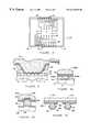
- FIG. 1is a plan view of a prior art semiconductor wafer containing multiple semiconductor dice
- FIG. 2is a plan view of a prior art semiconductor die illustrating contacts on the die and exemplary functional designations for the contacts;
- FIG. 3is a schematic cross sectional view of a test system constructed in accordance with the invention.
- FIG. 4is an enlarged cross sectional view taken along section line 4 — 4 of FIG. 3 illustrating a probe card constructed in accordance with the invention
- FIG. 5is an enlarged cross sectional view taken along section line 5 — 5 of FIG. 3 following contact of the probe card and wafer and illustrating probe card contacts electrically engaging wafer contacts;
- FIG. 5Ais an enlarged cross sectional view equivalent to FIG. 5 of an alternate embodiment probe card contact electrically engaging bumped contacts on the wafer;
- FIG. 5Bis an enlarged cross sectional view equivalent to FIG. 5 of an alternate embodiment probe card contact electrically engaging the contacts on the wafer;
- FIG. 5Cis an enlarged cross sectional view equivalent to FIG. 5 of alternate embodiment probe card contacts
- FIG. 6Ais a schematic plan view of resistivity contacts on the probe card and wafer contacts on the wafer configured for electrical engagement with the resistivity contacts;
- FIG. 6Bis a schematic electrical diagram of a resistivity measuring circuit
- FIG. 7is a flow diagram of a test method performed in accordance with the invention.
- FIGS. 8A-8Dare schematic cross sectional views illustrating process steps in fabricating the probe card embodiment of FIG. 5 C.
- a prior art semiconductor wafer 10includes multiple semiconductor dice 12 fabricated using processes that are well known in the art.
- the wafer 10also includes multiple wafer contacts 14 .
- the contacts 14comprise metal bond pads in electrical communication with integrated circuits contained on the dice 14 .
- each die 12includes twenty eight contacts 14 with the functional designations indicated in FIG. 2 .
- the number and functional arrangements of the contacts 14are merely exemplary, and other arrangements are possible.
- the dice 12can be used to fabricate semiconductor packages.
- the contacts 14can be wire bonded to lead fingers formed on a leadframe.
- the singulated dice 12can also be used in unpackaged form as known good die (KGD).
- the contacts 14can be wire bonded to a substrate, such as a printed circuit board, or alternately flip chip mounted using reflowed solder bumps.
- the singulated dice 12can also be included in chip scale packages.
- interconnectssuch as beam leads electrically contact the contacts 14 to establish electrical communication with mating external contacts on a substrate.
- test system 16constructed in accordance with the invention, and configured to test the dice 12 contained on the wafer 10 is shown.
- the test system 16includes a probe card 20 having probe contacts 22 configured to make temporary electrical connections with the wafer contacts 14 .
- the test system 16also includes a wafer handler 18 wherein the probe card 20 is mounted.
- the test system 16includes a tester 26 configured to apply test signals through the probe card 20 to the wafer 10 and to analyze the resultant signals. Suitable testers 26 are commercially available from Teradyne as well as other manufacturers.
- the wafer handler 18includes a test head 30 wherein the probe card 20 is mounted.
- the wafer handler 18also includes a wafer chuck 24 configured to move in X and Y directions to align the wafer 10 with the probe card 20 , and in the Z direction to move the wafer 10 into contact with the probe card 20 .
- One suitable wafer handler 18is manufactured by Electroglass and is designated a Model 4080.
- the test system 16also includes a prober interface board 28 for routing test signals from the tester 26 to the probe card 20 .
- the prober interface board 28can be mounted to the test head 30 of the wafer handler 18 .
- the prober interface board 28can be in electrical communication with tester pin electronics 32 physically located in the test head 30 .
- the tester pin electronics 32provide separate electrical paths 34 from test circuitry 33 and resistivity measuring circuitry 38 contained in the tester 26 , to the prober interface board 28 .
- the wafer handler 18includes a probe card fixture 62 , a force applying fixture 64 and a force applying mechanism 66 . These items can be components of a conventional wafer handler as previously described.
- the force applying mechanism 66presses against a pressure plate 68 and a compressible member 70 to bias the probe card 20 against the wafer 10 .
- the compressible member 70can be formed of an elastomeric material such as silicone, butyl rubber, or fluorosilicone; in foam, gel, solid or molded configurations.
- a flexible membrane 72is bonded to the probe card 20 and to the probe card fixture 62 .
- the flexible membrane 72functions to physically attach the probe card 20 to the probe card fixture 62 .
- the flexible membrane 72functions to provide electrical paths from the contacts 22 to the probe card fixture 62 and prober interface board 28 .
- the flexible membrane 72can be formed of thin flexible materials to allow movement of the probe card 20 in z-directions.
- the flexible membrane 72can be formed of a flexible multi layered material similar to TAB tape.
- the flexible membrane 72comprises a layer of polymer tape having metal conductors 84 (FIG. 6A) thereon. Bonded connections are formed between the conductors 84 on the membrane 72 and corresponding conductors 74 on the probe card fixture 62 . In addition, bonded connections are formed between the conductors 84 on the membrane 72 and the bonding pads 44 on the probe card 20 .
- the wafer handler 18includes spring loaded electrical connectors 76 which are in electrical communication with the prober interface board 28 .
- spring loaded electrical connector 76is manufactured by Pogo Industries of Kansas City, Mo. under the trademark “POGO PINS”.
- the electrical connectors 76electrically communicate with corresponding conductors on the probe card fixture 62 .
- probe card mounting arrangement shown in FIG. 3, as well as others,are described in U.S. Pat. No. 6,060,891, entitled “Probe Card For Semiconductor Wafers And Method And System For Testing Wafers”, incorporated herein by reference.
- these mounting arrangementsare merely exemplary and the probe card 20 can be mounted in a conventional manner on a commercially available wafer handler.
- the probe contacts 22 on the probe card 20are arranged in patterns corresponding to the patterns of the wafer contacts 14 .
- Each pattern of probe contacts 22represents a single test site S.
- only one test site S on the probe card 20is illustrated.
- the probe card 20can include multiple patterns of probe contacts 22 forming multiple test sites S to accommodate testing of multiple dice 12 at the same time.
- the patterns of probe contacts 22must exactly match the patterns of the wafer contacts 14 .
- the stepping distancei.e., x-y repeat and pattern spacing
- the software that controls the stepping processmust be able to pick valid test sites. For example, when testing at the edges of a round wafer with a probe card that includes rectangular or square patterns of probe contacts 22 , some patterns of probe contacts 22 will not have an associated device under test. It is also desirable to not have probe contacts 22 contacting a passivation layer on the dice 12 as this can damage the contacts 22 .
- the probe card 20includes patterns of conductors 36 in electrical communication with the probe contacts 22 .
- the probe contacts 22 and conductors 36are formed on a substrate 40 of the probe card 20 .
- the substrate 40can be formed of a rigid material able to resist deflection and buckling during test procedures using the probe card 20 .
- Preferred materialsinclude silicon, gallium arsenide, ceramic and glass filled resins, such as FR- 4 . In addition to being rigid, these materials have a coefficient of thermal expansion (CTE) closely matching that of the semiconductor wafer 10 .
- CTEcoefficient of thermal expansion
- the substrate 40comprises silicon.
- an electrically insulating layer 42(FIG. 5 ), such as SiO 2 , can be formed on the substrate 40 to provide insulation for the probe contacts 22 and conductors 36 .
- the substrate 40formed of an electrically insulating material, such as ceramic, the insulating layer 42 is not required.
- the conductors 36are formed on the substrate 40 to provide electrical paths from the test circuitry 33 (FIG. 3) and the resistivity measuring circuitry 38 (FIG. 3) to the probe contacts 22 .
- the conductors 36are preferably formed of a highly conductive metal such as copper, aluminum, titanium, tantalum, tungsten, molybdenum or alloys of these metals.
- the conductors 36can be formed as a single layer of metal, or as a bi-metal stack.
- the conductors 36can be formed using a thin film deposition process (e.g., CVD, patterning, etching), or using a thick film deposition process (e.g., screen printing, stenciling).
- the conductors 36also include bonding pads 44 located along the peripheral edges of the probe card 20 .
- the bonding pads 44provide bonding sites for forming separate electrical paths from a probe card fixture 62 (FIG. 1) to each of the conductors 36 .
- the bonding pads 44are located on recessed surfaces 46 of the substrate 40 to provide clearance for TAB bonds, wire bonds or other electrical connections to the bonding pads 44 .
- the probe contacts 22can be formed as raised members that project from a surface of the substrate 40 .
- the raised probe contacts 22help to provide a separation distance between the probe card 20 and the wafer 10 to clear any particulate contaminants that may be present on the opposing surfaces.
- the probe contacts 22can include penetrating projections 50 adapted to penetrate the wafer contacts 14 to a limited penetration depth.
- the penetrating projections 50have a height that is less than a thickness of the wafer contacts 14 . For thin film aluminum wafer contacts 14 , this thickness will typically be less than 2.0 ⁇ m.
- surfaces 52 at the tips of the probe contacts 22provide stop planes for limiting penetration of the probe contacts 22 into the wafer contacts 14 . These stop plane surfaces 52 , along with the dimensions of the penetrating projections 50 , insures that the probe contacts 22 minimally damage the wafer contacts 14 during a test procedure.
- the probe contacts 22 and penetrating projections 50can be formed integrally with the substrate 40 using a semiconductor fabrication process such as bulk micromachining. Such a process permits the probe contacts 22 , and penetrating projections 50 , to be formed accurately in a dense array.
- Each probe contact 22is covered with a conductive layer 54 in electrical communication with a conductor 36 .
- the conductive layers 54 for all of the probe contacts 22can be formed of a metal layer deposited and patterned to cover the probe contacts 22 , or other selected areas of the substrate 40 .
- the conductive layers 54 for the probe contacts 22can be formed of aluminum, copper, titanium, tungsten, tantalum, platinum, molybdenum, cobalt, nickel, gold, iridium or alloys of these metals. Some of these materials such as gold and platinum are non-reactive so that material transfer between the probe contacts 22 and wafer contacts 14 can be minimized.
- the conductive layers 54can also be a metal silicide or a conductive material such as polysilicon.
- the conductive layers 54can be formed as a bi-metal stack comprising a base layer and a non-reactive and oxidation resistant outer layer such as gold or platinum.
- the conductive layers 54can be formed using a metallization process comprising deposition (e.g., CVD), followed by photo patterning and etching.
- the conductive layer 54 for each probe contact 22is in electrical communication with a corresponding conductor 36 formed on the interconnect substrate 18 .
- the conductive layers 54 and conductors 36can be formed at the same time using the same metallization process. Alternately, the conductive layers 54 can be formed of a different metal than the conductors 36 using separate metallization process.
- a process for fabricating the probe contacts 22is described in U.S. Pat. No. 5,483,741, incorporated herein by reference.
- an alternate embodiment probe contact 22 Bis configured to electrically engage wafer contacts 14 B having solder bumps 56 formed thereon.
- the probe contacts 22 Bpermit bumped dice 12 B to be tested.
- the probe contact 22 Bcomprises an indentation formed in a substrate 40 B.
- the substrate 40 Bcan comprise silicon, gallium arsenide or ceramic.
- the indentationcan be etched or machined to a required size and shape, and then covered with a conductive layer 54 B.
- the probe contact 22 Bis configured to retain the solder bump 56 .
- the conductive layer 54 B for the probe contact 22 Bis in electrical communication with a conductor equivalent to the conductors 36 previously described. Further details of probe contacts 22 B are described in U.S. Pat. No. 5,962,921, entitled “Interconnect Having Recessed Contact Members With Penetrating Blades For Testing Semiconductor Dice And Packages With Contact Bumps”, incorporated herein by reference.
- an alternate embodiment probe contact 22 MBcomprises a metal microbump formed on a polymer film 58 similar to multi layered TAB tape.
- a conductor 36 MBis formed on an opposing side of the polymer film 58 in electrical communication with the contact 22 MB.
- a compliant adhesive layer 60attaches the polymer film 58 to a substrate 40 MB.
- an insulating layer 42 Bcan also be provided on the substrate 40 MB. Further details of probe contact 22 MB are described in U.S. Pat. No. 5,678,301, entitled “Method For Forming An Interconnect For Testing Unpackaged Semiconductor Dice”.
- probe contacts 22 Care illustrated.
- the probe contacts 22 Care formed on a substrate 40 C having an insulating layer 42 C formed thereon.
- the probe contacts 22 Care in electrical communication with conductors 36 C.
- a mask layer 80is formed on the conductors 36 C, and the probe contacts 22 C are formed in openings 82 in the mask layer 80 . Further details of the probe contacts 22 C, including a fabrication process, will subsequently be described with reference to FIGS. 8A-8D.
- resistivity contacts 22 - 1 , 22 - 2(FIG. 6A) and resistivity measuring circuit 38 (FIG. 6B) are illustrated.
- the resistivity measuring circuit 38can be included in a conventional digital multimeter contained within the tester 26 . This type of multimeter is commercially available from Keithley Instruments, Cleveland, Ohio, and other instrument manufacturers.
- Resistivity contact 22 - 1is in electrical communication with a source hi conductor 36 - 1 A and associated bonding pad 44 - 1 A. Resistivity contact 22 - 1 is also in electrical communication with a sense hi conductor 36 - 1 B and associated bonding pad 44 - 1 B. Resistivity contact 22 - 2 is in electrical communication with a source low conductor 36 - 2 A and associated bonding pad 44 - 2 A. Resistivity contact 22 - 2 is also in electrical communication with a sense low conductor 36 - 2 B and associated bonding pad 44 - 2 B.
- the resistivity contacts 22 - 1 , 22 - 2 , and bonding pads 44 - 1 A, 44 - 1 B, 44 - 2 B, 44 - 2 Aform a four point Kelvin structure 86 .
- the bonding pads 44 - 1 A, 44 - 1 B, 44 - 2 B, 44 - 2 Aare in electrical communication with conductors 84 on the flexible membrane 72 .
- the conductors 84are in electrical communication with the resistivity measuring circuit 38 contained in the tester 26 .
- the resistivity contacts 22 - 1 , 22 - 2are configured to electrically engage wafer contacts 14 Vcc- 1 , 14 Vcc- 2 .
- the wafer contacts 14 Vcc- 1 , 14 Vcc- 2are in electrical communication with one another via internal traces 88 contained within the particular die 12 on which the wafer contacts 14 Vcc are formed.
- Vss contacts on the die 12can be utilized instead of wafer contacts 14 Vcc- 1 , 14 Vcc- 2 . This is because the Vss contacts on the die 12 are also in electrical communication via internal traces.
- an unknown resistance R x(FIG. 6B) between the resistivity contacts 22 - 1 , 22 - 2 can be measured by applying a test current from source terminals (source Hi, source Lo) through a known resistance R L to the resistivity contacts 22 - 1 , 22 - 2 .
- a sense currentcan be applied from sense terminals (sense Hi, sense Lo) through known resistances to the resistivity contacts 22 - 1 , 22 - 2 .
- the sense currentis very low (e.g., pico-amps) such that the I-R drop is low and the voltage seen by the sense terminals (sense Hi, sense Lo) is the same as the voltage developed across R x .
- One method for evaluating the resistance R xis by making resistance measurements when the probe card 20 is new, or immediately following cleaning. These initial values for R x can then be compared to measured values for R x during test procedures using the probe card 20 .
- the contact resistances (Rc 1 and Rc 2 ) between the resistivity contacts 22 - 1 , 22 - 2 and the wafer contacts 14 Vcc- 1 , 14 Vcc- 2is a major component of the resistance R x . Accordingly, a high value for R x may indicate that the electrical connections between the probe contacts 22 and wafer contacts 14 are also substandard. This may be due to misalignment of the probe card 20 and wafer 10 or due to contaminants on the mating surfaces thereof.
- the resistivity of the contacts 22 - 1 , 22 - 2 , and of the contacts 14 Vcc- 1 , 14 Vcc- 2are also components of the resistance R x . Accordingly, a high value for R x may indicate contaminated or dirty probe contacts 22 , or wafer contacts 14 .
- the resistivity measuring circuitry 38(FIG. 6B) can be used to evaluate the contact resistances (Rc 1 and Rc 2 ) between the resistivity contacts 22 - 1 , 22 - 2 (FIG. 6A) and the selected contacts 14 Vcc- 1 , 14 Vcc- 2 on the wafer 10 .
- the measured contact resistancecan be used to provide feedback to the tester 26 for generating test signals. For example, with high contact resistance the test signals to the probe card contacts 22 can be adjusted to compensate for the high contact resistance. The adjusted test signals can then be analyzed by the tester 26 . Also, if the measured contact resistance is too high an operator of the probe test system 16 can be notified. If the contact resistance is within an acceptable range, the test signals can be analyzed without adjustment. The measured contact resistance can also be an indication that the probe card contacts 22 require cleaning, or that the probe card contacts 22 and the wafer contacts 14 are misaligned.
- the conductors 36 Ccomprise a bi-metal stack including a barrier layer 94 and a conductive layer 92 .
- the substrate 40 Cis formed or provided.
- the substrate 40 Ccomprises silicon.
- the insulating layer 42 Ccan be formed on the substrate 40 C to protect and insulate the substrate 40 C.
- the insulating layer 42 Ccan be formed of an electrically insulating material such as an oxide, dielectric or insulating polymer.
- a representative thickness for the insulating layer 42 Ccan be from about 1000 ⁇ to 10 ⁇ m.
- the insulating layer 42 Ccan be silicon dioxide (SiO 2 ) deposited using a CVD process.
- TEOStetraethylorthosilane
- the insulating layer 42 Ccan also be formed by exposing the substrate 40 C to an oxidizing atmosphere in a reaction chamber.
- the insulating layer 42 Ccan be formed of a dielectric material, such as Si 3 N 4 , deposited using CVD or other deposition process.
- the insulating layer 42 Ccan be formed of polyimide, or similar electrically insulating polymeric material, spun on or otherwise deposited on the substrate 40 C.
- the natural resiliency of the materialallows the insulating layer 42 C to function as a compliant layer. This compliancy will allow the subsequently formed contacts 22 C (FIG. 8D) to flex to accommodate dimensional variations in the z-direction.
- the conductors 36 Ccan be formed on the insulating layer 42 C.
- the conductors 36 Cinclude the barrier layer 94 formed on the insulating layer 42 C and the conductive layer 92 formed on the barrier layer 94 .
- the barrier layer 94can comprise an inert metal such as a titanium (Ti) or an alloy of titanium such as TiW or TiN. Other suitable materials for the barrier layer 94 include tungsten (W), and alloys of tungsten such as WN.
- the barrier layer 94provides adhesion to the substrate 40 C and prevents diffusion of the conductive layer 92 into the substrate 40 C.
- the barrier layer 94can be blanket deposited using a suitable deposition process such as CVD, sputtering, or plating.
- a representative thickness for the barrier layer 94is from 200 ⁇ to 1 ⁇ m.
- the conductive layer 92can then be blanket deposited on the barrier layer 94 .
- the conductive layer 92is preferably formed of a highly conductive metal such as copper, aluminum, titanium, tantalum, tungsten, molybdenum or alloys of these metals.
- the conductive layer 92can be blanket deposited on the barrier layer 94 by CVD or sputtering.
- the conductive layer 92can also be deposited on the barrier layer 94 using electroplating or electroless plating.
- the barrier layer 94can function as a nucleation surface for forming the conductive layer 92 .
- the conductive layer 92can function as a nucleation surface for subsequent formation of contacts 22 C (FIG. 8 C).
- a representative thickness for the conductive layer 92can be from about 200 ⁇ to 10 ⁇ m.
- a layer of resist 90is deposited on the conductive layer 92 and developed.
- the layer of resist 90can be deposited using a spin-on process and then soft baked to drive out solvents.
- a typical thickness for the layer of resist 90can be about 1,000 ⁇ to 30,000 ⁇ .
- the layer of resist 90can be aligned with a mask and exposed using collimated UV light.
- the layer of resist 90(FIG. 8A) can be developed to form a resist mask (not shown) which is used to etch the conductive layer 92 and barrier layer 94 to form the pattern of bi-metal conductors 36 C.
- a suitable wet etch processcan be used to etch the layers to form the conductors 36 C.
- a wet etchantsuch as H 3 PO 4 followed by NH 4 OH can be used to etch the pattern of conductors 36 C.
- the layer of resist 90can be stripped using a suitable wet etchant along with organic ashing.
- a solventsuch as acetone, methylethylketone or 1-methylethylketone can be used.
- a solution that will not attack the underlying metalcan be used.
- the mask layer 80can be deposited.
- the mask layercomprises an elastomeric material.
- One suitable material for forming the mask layer 80comprises polyimide deposited using a spin on process.
- a representative thickness of the mask layer 80can be from 1 to 5 mils.
- the mask layer 80can be patterned and etched to form the pattern of openings 82 in alignment with the conductors 36 C.
- the openings 82are located near a terminal end of the conductors 36 C.
- the location of the openings 82corresponds to the pattern of the wafer contacts 14 (FIG. 2 ). Patterning and etching the openings 32 for the mask layer 30 can be performed using a resist mask as previously described and a suitable wet etchant.
- the contacts 22 Care formed on the conductors 36 C by filling the openings 82 with metal.
- Suitable metalsinclude copper, nickel, gold and palladium.
- One method for forming the contacts 22 Ccomprises an electroplating process. Equipment and solutions used for electroplating the above metals are well known in the art.
- electroless platingan aqueous solution comprising metal ions and reducing agents is used. These solutions are also known in the art.
- electroless plating of nickelcan be performed using a solution containing Ni ions and a reducing agent such as hypophosphite or dimethylamine borane.
- Electroless plating of coppercan be performed using a solution containing Cu ions and a suitable reducing agent.
- a cap layer 96can optionally be formed on the exposed tip portions of the contacts 22 C.
- the cap layer 96can be formed of an inert metal that will inhibit oxidation and diffusion of the metal which forms the contacts 22 C.
- the cap layer 96can be formed using an electroplating process, an electroless plating process, or a metallization process (e.g., deposition, photopatterning, etching). Suitable metals for forming the cap layer 96 include palladium, gold, and platinum. For applications in which a hard metal is required the cap layer 96 can comprise tungsten.
- a representative thickness for the cap layer 96can be from 100 ⁇ to 2 ⁇ m.
- the mask layer 80can be partially stripped, as previously described, leaving a thin layer insulating the conductors 36 C.
- the inventionprovides an improved probe card for testing semiconductors wafers, a system for testing wafers using the probe card, a method for testing wafers using the probe card, and a method for fabricating the probe card.
- the probe cardincludes resistivity contacts configured for use with resistivity measuring circuitry.
Landscapes
- Physics & Mathematics (AREA)
- General Physics & Mathematics (AREA)
- Geometry (AREA)
- Testing Or Measuring Of Semiconductors Or The Like (AREA)
- Measuring Leads Or Probes (AREA)
Abstract
Description
Claims (9)
Priority Applications (1)
| Application Number | Priority Date | Filing Date | Title |
|---|---|---|---|
| US09/418,229US6218848B1 (en) | 1998-02-25 | 1999-10-14 | Semiconductor probe card having resistance measuring circuitry and method of fabrication |
Applications Claiming Priority (2)
| Application Number | Priority Date | Filing Date | Title |
|---|---|---|---|
| US09/030,181US6181144B1 (en) | 1998-02-25 | 1998-02-25 | Semiconductor probe card having resistance measuring circuitry and method fabrication |
| US09/418,229US6218848B1 (en) | 1998-02-25 | 1999-10-14 | Semiconductor probe card having resistance measuring circuitry and method of fabrication |
Related Parent Applications (1)
| Application Number | Title | Priority Date | Filing Date |
|---|---|---|---|
| US09/030,181DivisionUS6181144B1 (en) | 1998-02-25 | 1998-02-25 | Semiconductor probe card having resistance measuring circuitry and method fabrication |
Publications (1)
| Publication Number | Publication Date |
|---|---|
| US6218848B1true US6218848B1 (en) | 2001-04-17 |
Family
ID=21852925
Family Applications (2)
| Application Number | Title | Priority Date | Filing Date |
|---|---|---|---|
| US09/030,181Expired - LifetimeUS6181144B1 (en) | 1998-02-25 | 1998-02-25 | Semiconductor probe card having resistance measuring circuitry and method fabrication |
| US09/418,229Expired - LifetimeUS6218848B1 (en) | 1998-02-25 | 1999-10-14 | Semiconductor probe card having resistance measuring circuitry and method of fabrication |
Family Applications Before (1)
| Application Number | Title | Priority Date | Filing Date |
|---|---|---|---|
| US09/030,181Expired - LifetimeUS6181144B1 (en) | 1998-02-25 | 1998-02-25 | Semiconductor probe card having resistance measuring circuitry and method fabrication |
Country Status (1)
| Country | Link |
|---|---|
| US (2) | US6181144B1 (en) |
Cited By (51)
| Publication number | Priority date | Publication date | Assignee | Title |
|---|---|---|---|---|
| US6297653B1 (en) | 1999-06-28 | 2001-10-02 | Micron Technology, Inc. | Interconnect and carrier with resistivity measuring contacts for testing semiconductor components |
| US6337577B1 (en) | 1998-05-11 | 2002-01-08 | Micron Technology, Inc. | Interconnect and system for testing bumped semiconductor components with on-board multiplex circuitry for expanding tester resources |
| US6356098B1 (en) | 1998-02-23 | 2002-03-12 | Micron Technology, Inc. | Probe card, test method and test system for semiconductor wafers |
| US20020078409A1 (en)* | 2000-12-19 | 2002-06-20 | Andrew Marshall | Method and system for detecting an outlying resistance in a plurality of resistive elements |
| US6419844B1 (en) | 1998-05-26 | 2002-07-16 | Micron Technology, Inc. | Method for fabricating calibration target for calibrating semiconductor wafer test systems |
| US20020105348A1 (en)* | 2000-12-12 | 2002-08-08 | Resor Griffith L. | Electronically measuring pin-to-pad alignment using resistive pads |
| US6503765B1 (en)* | 2001-07-31 | 2003-01-07 | Xilinx, Inc. | Testing vias and contacts in integrated circuit fabrication |
| US20030048624A1 (en)* | 2001-08-22 | 2003-03-13 | Tessera, Inc. | Low-height multi-component assemblies |
| US20030082936A1 (en)* | 2001-10-25 | 2003-05-01 | Agilent Technologies, Inc. | Connection box, system, and method for evaluating a DUT board |
| US20030107118A1 (en)* | 2001-10-09 | 2003-06-12 | Tessera, Inc. | Stacked packages |
| US6677776B2 (en) | 1998-05-11 | 2004-01-13 | Micron Technology, Inc. | Method and system having switching network for testing semiconductor components on a substrate |
| US6677744B1 (en)* | 2000-04-13 | 2004-01-13 | Formfactor, Inc. | System for measuring signal path resistance for an integrated circuit tester interconnect structure |
| US20040031972A1 (en)* | 2001-10-09 | 2004-02-19 | Tessera, Inc. | Stacked packages |
| US6696850B1 (en) | 2002-10-02 | 2004-02-24 | Interconnect Devices, Inc. | Contact probe with off-centered back-drilled aperture |
| US6717423B1 (en)* | 2002-10-09 | 2004-04-06 | Lsi Logic Corporation | Substrate impedance measurement |
| US20040099938A1 (en)* | 2002-09-11 | 2004-05-27 | Tessera, Inc. | Assemblies having stacked semiconductor chips and methods of making same |
| US20040104470A1 (en)* | 2002-08-16 | 2004-06-03 | Tessera, Inc. | Microelectronic packages with self-aligning features |
| WO2004070405A1 (en)* | 2003-02-05 | 2004-08-19 | Systems On Silicon Manufacturing Co. Pte. Ltd. | Probe card needle cleaning frequency optimization |
| US20040164758A1 (en)* | 2003-02-21 | 2004-08-26 | Nagar Mohan R. | Substrate impedance measurement |
| US20040217461A1 (en)* | 2002-08-05 | 2004-11-04 | Tessera, Inc. | Microelectronic adaptors, assemblies and methods |
| US20040217762A1 (en)* | 2003-04-30 | 2004-11-04 | Gifford Carl B. | Apparatus and methods for measuring resistance of conductive layers |
| US20040251925A1 (en)* | 2003-05-30 | 2004-12-16 | Aritharan Thurairajaratnam | Measurement of package interconnect impedance using tester and supporting tester |
| US6885106B1 (en) | 2001-01-11 | 2005-04-26 | Tessera, Inc. | Stacked microelectronic assemblies and methods of making same |
| US20050116734A1 (en)* | 2003-12-02 | 2005-06-02 | Savagaonkar Uday R. | Dynamic overdrive compensation test system and method |
| US20050164527A1 (en)* | 2003-04-11 | 2005-07-28 | Radza Eric M. | Method and system for batch forming spring elements in three dimensions |
| US20050173796A1 (en)* | 2001-10-09 | 2005-08-11 | Tessera, Inc. | Microelectronic assembly having array including passive elements and interconnects |
| US20050204538A1 (en)* | 2004-03-19 | 2005-09-22 | Epic Technology Inc. | Contact and method for making same |
| US20050205988A1 (en)* | 2004-03-19 | 2005-09-22 | Epic Technology Inc. | Die package with higher useable die contact pad area |
| US20050208788A1 (en)* | 2004-03-19 | 2005-09-22 | Dittmann Larry E | Electrical connector in a flexible host |
| US20060103399A1 (en)* | 2004-11-02 | 2006-05-18 | Yian-Liang Kuo | Apparatus and method for testing conductive bumps |
| US20060125500A1 (en)* | 2003-10-14 | 2006-06-15 | Watkins Charles M | Compliant contact structure |
| US7064564B2 (en)* | 2001-02-01 | 2006-06-20 | Antares Contech, Inc. | Bundled probe apparatus for multiple terminal contacting |
| US20060132162A1 (en)* | 2004-12-16 | 2006-06-22 | Romi Mayder | Mock wafer, system calibrated using mock wafer, and method for calibrating automated test equipment |
| US20060258183A1 (en)* | 2003-04-11 | 2006-11-16 | Neoconix, Inc. | Electrical connector on a flexible carrier |
| US20060258182A1 (en)* | 2004-07-20 | 2006-11-16 | Dittmann Larry E | Interposer with compliant pins |
| US20070050738A1 (en)* | 2005-08-31 | 2007-03-01 | Dittmann Larry E | Customer designed interposer |
| US20070054515A1 (en)* | 2003-04-11 | 2007-03-08 | Williams John D | Method for fabricating a contact grid array |
| US20070134949A1 (en)* | 2005-12-12 | 2007-06-14 | Dittmann Larry E | Connector having staggered contact architecture for enhanced working range |
| US20070141863A1 (en)* | 2003-04-11 | 2007-06-21 | Williams John D | Contact grid array system |
| US20070218710A1 (en)* | 2003-06-11 | 2007-09-20 | Brown Dirk D | Structure and process for a contact grid array formed in a circuitized substrate |
| US20070259539A1 (en)* | 2003-04-11 | 2007-11-08 | Brown Dirk D | Method and system for batch manufacturing of spring elements |
| US20070275572A1 (en)* | 2003-12-08 | 2007-11-29 | Williams John D | Connector for making electrical contact at semiconductor scales |
| US20080042250A1 (en)* | 2006-08-18 | 2008-02-21 | Tessera, Inc. | Stacked microelectronic assemblies and methods therefor |
| US20080042274A1 (en)* | 2002-09-06 | 2008-02-21 | Tessera, Inc. | Components, methods and assemblies for stacked packages |
| US20080156352A1 (en)* | 2006-12-28 | 2008-07-03 | Texas Instruments Incorporated | Contact mechanism cleaning |
| US20110081154A1 (en)* | 2009-10-06 | 2011-04-07 | Kabushiki Kaisha Toshiba | Apparatus for detecting connector connection state |
| US20110279137A1 (en)* | 2010-05-12 | 2011-11-17 | Stmicroelectronics S.R.L. | Probes for testing integrated electronic circuits and corresponding production method |
| US8641428B2 (en) | 2011-12-02 | 2014-02-04 | Neoconix, Inc. | Electrical connector and method of making it |
| US20140232421A1 (en)* | 2012-11-12 | 2014-08-21 | Mpi Corporation | Probe card of low power loss |
| USRE45463E1 (en) | 2003-11-12 | 2015-04-14 | Tessera, Inc. | Stacked microelectronic assemblies with central contacts |
| US9680273B2 (en) | 2013-03-15 | 2017-06-13 | Neoconix, Inc | Electrical connector with electrical contacts protected by a layer of compressible material and method of making it |
Families Citing this family (117)
| Publication number | Priority date | Publication date | Assignee | Title |
|---|---|---|---|---|
| US5345170A (en)* | 1992-06-11 | 1994-09-06 | Cascade Microtech, Inc. | Wafer probe station having integrated guarding, Kelvin connection and shielding systems |
| US6380751B2 (en)* | 1992-06-11 | 2002-04-30 | Cascade Microtech, Inc. | Wafer probe station having environment control enclosure |
| US20020053734A1 (en) | 1993-11-16 | 2002-05-09 | Formfactor, Inc. | Probe card assembly and kit, and methods of making same |
| US6232789B1 (en)* | 1997-05-28 | 2001-05-15 | Cascade Microtech, Inc. | Probe holder for low current measurements |
| US5561377A (en)* | 1995-04-14 | 1996-10-01 | Cascade Microtech, Inc. | System for evaluating probing networks |
| US6483328B1 (en) | 1995-11-09 | 2002-11-19 | Formfactor, Inc. | Probe card for probing wafers with raised contact elements |
| US5914613A (en)* | 1996-08-08 | 1999-06-22 | Cascade Microtech, Inc. | Membrane probing system with local contact scrub |
| US6002263A (en) | 1997-06-06 | 1999-12-14 | Cascade Microtech, Inc. | Probe station having inner and outer shielding |
| US7282240B1 (en)* | 1998-04-21 | 2007-10-16 | President And Fellows Of Harvard College | Elastomeric mask and use in fabrication of devices |
| US6256882B1 (en)* | 1998-07-14 | 2001-07-10 | Cascade Microtech, Inc. | Membrane probing system |
| US6578264B1 (en) | 1999-06-04 | 2003-06-17 | Cascade Microtech, Inc. | Method for constructing a membrane probe using a depression |
| US6445202B1 (en) | 1999-06-30 | 2002-09-03 | Cascade Microtech, Inc. | Probe station thermal chuck with shielding for capacitive current |
| US6838890B2 (en) | 2000-02-25 | 2005-01-04 | Cascade Microtech, Inc. | Membrane probing system |
| US6893850B2 (en)* | 2000-03-17 | 2005-05-17 | President And Fellows Of Harvard College | Method for cell patterning |
| US6476630B1 (en) | 2000-04-13 | 2002-11-05 | Formfactor, Inc. | Method for testing signal paths between an integrated circuit wafer and a wafer tester |
| US6724209B1 (en) | 2000-04-13 | 2004-04-20 | Ralph G. Whitten | Method for testing signal paths between an integrated circuit wafer and a wafer tester |
| US6622103B1 (en) | 2000-06-20 | 2003-09-16 | Formfactor, Inc. | System for calibrating timing of an integrated circuit wafer tester |
| US6965226B2 (en)* | 2000-09-05 | 2005-11-15 | Cascade Microtech, Inc. | Chuck for holding a device under test |
| US6914423B2 (en)* | 2000-09-05 | 2005-07-05 | Cascade Microtech, Inc. | Probe station |
| JP2002082130A (en) | 2000-09-06 | 2002-03-22 | Hitachi Ltd | Semiconductor device inspection apparatus and method of manufacturing the same |
| DE20114544U1 (en) | 2000-12-04 | 2002-02-21 | Cascade Microtech, Inc., Beaverton, Oreg. | wafer probe |
| US6791344B2 (en)* | 2000-12-28 | 2004-09-14 | International Business Machines Corporation | System for and method of testing a microelectronic device using a dual probe technique |
| US7143500B2 (en) | 2001-06-25 | 2006-12-05 | Micron Technology, Inc. | Method to prevent damage to probe card |
| EP1407280B1 (en)* | 2001-07-11 | 2005-11-23 | Formfactor, Inc. | Method of manufacturing a probe card |
| US6729019B2 (en)* | 2001-07-11 | 2004-05-04 | Formfactor, Inc. | Method of manufacturing a probe card |
| US6912778B2 (en)* | 2001-07-19 | 2005-07-05 | Micron Technology, Inc. | Methods of fabricating full-wafer silicon probe cards for burn-in and testing of semiconductor devices |
| US7355420B2 (en) | 2001-08-21 | 2008-04-08 | Cascade Microtech, Inc. | Membrane probing system |
| US6777964B2 (en)* | 2002-01-25 | 2004-08-17 | Cascade Microtech, Inc. | Probe station |
| US7352258B2 (en)* | 2002-03-28 | 2008-04-01 | Cascade Microtech, Inc. | Waveguide adapter for probe assembly having a detachable bias tee |
| US6894519B2 (en)* | 2002-04-11 | 2005-05-17 | Solid State Measurements, Inc. | Apparatus and method for determining electrical properties of a semiconductor wafer |
| KR100864916B1 (en)* | 2002-05-23 | 2008-10-22 | 캐스케이드 마이크로테크 인코포레이티드 | Probes for Testing Devices Under Test |
| US6847219B1 (en)* | 2002-11-08 | 2005-01-25 | Cascade Microtech, Inc. | Probe station with low noise characteristics |
| US6724205B1 (en) | 2002-11-13 | 2004-04-20 | Cascade Microtech, Inc. | Probe for combined signals |
| US7250779B2 (en) | 2002-11-25 | 2007-07-31 | Cascade Microtech, Inc. | Probe station with low inductance path |
| US6861856B2 (en)* | 2002-12-13 | 2005-03-01 | Cascade Microtech, Inc. | Guarded tub enclosure |
| US20100167561A1 (en)* | 2003-04-11 | 2010-07-01 | Neoconix, Inc. | Structure and process for a contact grid array formed in a circuitized substrate |
| US7221172B2 (en)* | 2003-05-06 | 2007-05-22 | Cascade Microtech, Inc. | Switched suspended conductor and connection |
| US7057404B2 (en)* | 2003-05-23 | 2006-06-06 | Sharp Laboratories Of America, Inc. | Shielded probe for testing a device under test |
| US7492172B2 (en)* | 2003-05-23 | 2009-02-17 | Cascade Microtech, Inc. | Chuck for holding a device under test |
| WO2004113935A2 (en)* | 2003-06-20 | 2004-12-29 | The Trustees Of Dartmouth College | Test fixture for impedance measurements |
| US7250626B2 (en)* | 2003-10-22 | 2007-07-31 | Cascade Microtech, Inc. | Probe testing structure |
| US7911218B2 (en)* | 2003-12-22 | 2011-03-22 | Robert Bosch Gmbh | Device and method for analyzing a sample plate |
| WO2005065258A2 (en)* | 2003-12-24 | 2005-07-21 | Cascade Microtech, Inc. | Active wafer probe |
| US7187188B2 (en) | 2003-12-24 | 2007-03-06 | Cascade Microtech, Inc. | Chuck with integrated wafer support |
| US7023231B2 (en)* | 2004-05-14 | 2006-04-04 | Solid State Measurements, Inc. | Work function controlled probe for measuring properties of a semiconductor wafer and method of use thereof |
| WO2005121824A2 (en)* | 2004-06-07 | 2005-12-22 | Cascade Microtech, Inc. | Thermal optical chuck |
| US7330041B2 (en) | 2004-06-14 | 2008-02-12 | Cascade Microtech, Inc. | Localizing a temperature of a device for testing |
| KR101157449B1 (en)* | 2004-07-07 | 2012-06-22 | 캐스케이드 마이크로테크 인코포레이티드 | Probe head having a membrane suspended probe |
| EP1789812A2 (en)* | 2004-09-13 | 2007-05-30 | Cascade Microtech, Inc. | Double sided probing structures |
| DE202005021436U1 (en)* | 2004-11-02 | 2008-02-14 | Cascade Microtech, Inc., Beaverton | Optically enhanced digital imaging system |
| US7656172B2 (en)* | 2005-01-31 | 2010-02-02 | Cascade Microtech, Inc. | System for testing semiconductors |
| US20060169897A1 (en)* | 2005-01-31 | 2006-08-03 | Cascade Microtech, Inc. | Microscope system for testing semiconductors |
| US7535247B2 (en)* | 2005-01-31 | 2009-05-19 | Cascade Microtech, Inc. | Interface for testing semiconductors |
| US7282941B2 (en)* | 2005-04-05 | 2007-10-16 | Solid State Measurements, Inc. | Method of measuring semiconductor wafers with an oxide enhanced probe |
| US7449899B2 (en)* | 2005-06-08 | 2008-11-11 | Cascade Microtech, Inc. | Probe for high frequency signals |
| JP5080459B2 (en)* | 2005-06-13 | 2012-11-21 | カスケード マイクロテック インコーポレイテッド | Wideband active / passive differential signal probe |
| TWI254972B (en)* | 2005-07-11 | 2006-05-11 | Siliconmotion Inc | Bond pad structure |
| US7609077B2 (en) | 2006-06-09 | 2009-10-27 | Cascade Microtech, Inc. | Differential signal probe with integral balun |
| US7764072B2 (en)* | 2006-06-12 | 2010-07-27 | Cascade Microtech, Inc. | Differential signal probing system |
| US7723999B2 (en)* | 2006-06-12 | 2010-05-25 | Cascade Microtech, Inc. | Calibration structures for differential signal probing |
| US7443186B2 (en)* | 2006-06-12 | 2008-10-28 | Cascade Microtech, Inc. | On-wafer test structures for differential signals |
| US7403028B2 (en) | 2006-06-12 | 2008-07-22 | Cascade Microtech, Inc. | Test structure and probe for differential signals |
| US7876114B2 (en)* | 2007-08-08 | 2011-01-25 | Cascade Microtech, Inc. | Differential waveguide probe |
| US20090201038A1 (en)* | 2008-02-11 | 2009-08-13 | Knickerbocker John U | Test head for functional wafer level testing, system and method therefor |
| US7924035B2 (en)* | 2008-07-15 | 2011-04-12 | Formfactor, Inc. | Probe card assembly for electronic device testing with DC test resource sharing |
| US7888957B2 (en)* | 2008-10-06 | 2011-02-15 | Cascade Microtech, Inc. | Probing apparatus with impedance optimized interface |
| US8410806B2 (en) | 2008-11-21 | 2013-04-02 | Cascade Microtech, Inc. | Replaceable coupon for a probing apparatus |
| US8319503B2 (en) | 2008-11-24 | 2012-11-27 | Cascade Microtech, Inc. | Test apparatus for measuring a characteristic of a device under test |
| US8441272B2 (en)* | 2008-12-30 | 2013-05-14 | Stmicroelectronics S.R.L. | MEMS probe for probe cards for integrated circuits |
| WO2010147939A1 (en) | 2009-06-17 | 2010-12-23 | Hsio Technologies, Llc | Semiconductor socket |
| WO2011153298A1 (en) | 2010-06-03 | 2011-12-08 | Hsio Technologies, Llc | Electrical connector insulator housing |
| US9536815B2 (en) | 2009-05-28 | 2017-01-03 | Hsio Technologies, Llc | Semiconductor socket with direct selective metalization |
| US9276336B2 (en) | 2009-05-28 | 2016-03-01 | Hsio Technologies, Llc | Metalized pad to electrical contact interface |
| US8955215B2 (en) | 2009-05-28 | 2015-02-17 | Hsio Technologies, Llc | High performance surface mount electrical interconnect |
| US9276339B2 (en) | 2009-06-02 | 2016-03-01 | Hsio Technologies, Llc | Electrical interconnect IC device socket |
| WO2010141264A1 (en)* | 2009-06-03 | 2010-12-09 | Hsio Technologies, Llc | Compliant wafer level probe assembly |
| US9603249B2 (en) | 2009-06-02 | 2017-03-21 | Hsio Technologies, Llc | Direct metalization of electrical circuit structures |
| WO2010141313A1 (en) | 2009-06-02 | 2010-12-09 | Hsio Technologies, Llc | Compliant printed circuit socket diagnostic tool |
| WO2011002709A1 (en) | 2009-06-29 | 2011-01-06 | Hsio Technologies, Llc | Compliant printed circuit semiconductor tester interface |
| US9196980B2 (en) | 2009-06-02 | 2015-11-24 | Hsio Technologies, Llc | High performance surface mount electrical interconnect with external biased normal force loading |
| US9699906B2 (en) | 2009-06-02 | 2017-07-04 | Hsio Technologies, Llc | Hybrid printed circuit assembly with low density main core and embedded high density circuit regions |
| US9613841B2 (en) | 2009-06-02 | 2017-04-04 | Hsio Technologies, Llc | Area array semiconductor device package interconnect structure with optional package-to-package or flexible circuit to package connection |
| US8912812B2 (en) | 2009-06-02 | 2014-12-16 | Hsio Technologies, Llc | Compliant printed circuit wafer probe diagnostic tool |
| US9320133B2 (en) | 2009-06-02 | 2016-04-19 | Hsio Technologies, Llc | Electrical interconnect IC device socket |
| US8988093B2 (en) | 2009-06-02 | 2015-03-24 | Hsio Technologies, Llc | Bumped semiconductor wafer or die level electrical interconnect |
| WO2010141296A1 (en) | 2009-06-02 | 2010-12-09 | Hsio Technologies, Llc | Compliant printed circuit semiconductor package |
| US9414500B2 (en) | 2009-06-02 | 2016-08-09 | Hsio Technologies, Llc | Compliant printed flexible circuit |
| US9136196B2 (en) | 2009-06-02 | 2015-09-15 | Hsio Technologies, Llc | Compliant printed circuit wafer level semiconductor package |
| US9054097B2 (en) | 2009-06-02 | 2015-06-09 | Hsio Technologies, Llc | Compliant printed circuit area array semiconductor device package |
| WO2012074963A1 (en) | 2010-12-01 | 2012-06-07 | Hsio Technologies, Llc | High performance surface mount electrical interconnect |
| US9184145B2 (en) | 2009-06-02 | 2015-11-10 | Hsio Technologies, Llc | Semiconductor device package adapter |
| US8610265B2 (en) | 2009-06-02 | 2013-12-17 | Hsio Technologies, Llc | Compliant core peripheral lead semiconductor test socket |
| US8525346B2 (en) | 2009-06-02 | 2013-09-03 | Hsio Technologies, Llc | Compliant conductive nano-particle electrical interconnect |
| US9930775B2 (en) | 2009-06-02 | 2018-03-27 | Hsio Technologies, Llc | Copper pillar full metal via electrical circuit structure |
| US9318862B2 (en) | 2009-06-02 | 2016-04-19 | Hsio Technologies, Llc | Method of making an electronic interconnect |
| US8987886B2 (en) | 2009-06-02 | 2015-03-24 | Hsio Technologies, Llc | Copper pillar full metal via electrical circuit structure |
| WO2010141298A1 (en) | 2009-06-02 | 2010-12-09 | Hsio Technologies, Llc | Composite polymer-metal electrical contacts |
| US9231328B2 (en) | 2009-06-02 | 2016-01-05 | Hsio Technologies, Llc | Resilient conductive electrical interconnect |
| US8955216B2 (en) | 2009-06-02 | 2015-02-17 | Hsio Technologies, Llc | Method of making a compliant printed circuit peripheral lead semiconductor package |
| US9232654B2 (en) | 2009-06-02 | 2016-01-05 | Hsio Technologies, Llc | High performance electrical circuit structure |
| WO2010141318A1 (en) | 2009-06-02 | 2010-12-09 | Hsio Technologies, Llc | Compliant printed circuit peripheral lead semiconductor test socket |
| WO2010147934A1 (en) | 2009-06-16 | 2010-12-23 | Hsio Technologies, Llc | Semiconductor die terminal |
| WO2010147782A1 (en) | 2009-06-16 | 2010-12-23 | Hsio Technologies, Llc | Simulated wirebond semiconductor package |
| US8984748B2 (en) | 2009-06-29 | 2015-03-24 | Hsio Technologies, Llc | Singulated semiconductor device separable electrical interconnect |
| US8758067B2 (en) | 2010-06-03 | 2014-06-24 | Hsio Technologies, Llc | Selective metalization of electrical connector or socket housing |
| US9689897B2 (en) | 2010-06-03 | 2017-06-27 | Hsio Technologies, Llc | Performance enhanced semiconductor socket |
| US10159154B2 (en) | 2010-06-03 | 2018-12-18 | Hsio Technologies, Llc | Fusion bonded liquid crystal polymer circuit structure |
| US9350093B2 (en) | 2010-06-03 | 2016-05-24 | Hsio Technologies, Llc | Selective metalization of electrical connector or socket housing |
| US9761520B2 (en) | 2012-07-10 | 2017-09-12 | Hsio Technologies, Llc | Method of making an electrical connector having electrodeposited terminals |
| JP6155725B2 (en)* | 2013-03-19 | 2017-07-05 | 富士電機株式会社 | Semiconductor device inspection method and semiconductor device manufacturing method using the same |
| US10506722B2 (en) | 2013-07-11 | 2019-12-10 | Hsio Technologies, Llc | Fusion bonded liquid crystal polymer electrical circuit structure |
| US10667410B2 (en) | 2013-07-11 | 2020-05-26 | Hsio Technologies, Llc | Method of making a fusion bonded circuit structure |
| US9612260B2 (en)* | 2014-09-10 | 2017-04-04 | Andre Olivier | Method and system for counting socket insertions of electronic integrated circuits |
| CN104407225B (en)* | 2014-11-29 | 2017-08-25 | 洛阳康耀电子有限公司 | A kind of indium oxide tin film hand-held probe test device and its method |
| US9559447B2 (en) | 2015-03-18 | 2017-01-31 | Hsio Technologies, Llc | Mechanical contact retention within an electrical connector |
| CN107885606B (en)* | 2016-09-30 | 2020-12-01 | 中芯国际集成电路制造(北京)有限公司 | Reliability evaluation method of interlayer interconnection component |
| KR20190021101A (en) | 2017-08-22 | 2019-03-05 | 삼성전자주식회사 | Probe card, test apparatus comprising the probe card, testing method for testing and manufacturing semiconductor using the probe card |
Citations (41)
| Publication number | Priority date | Publication date | Assignee | Title |
|---|---|---|---|---|
| US3809625A (en) | 1972-08-15 | 1974-05-07 | Gen Motors Corp | Method of making contact bumps on flip-chips |
| US4027935A (en) | 1976-06-21 | 1977-06-07 | International Business Machines Corporation | Contact for an electrical contactor assembly |
| US4161692A (en) | 1977-07-18 | 1979-07-17 | Cerprobe Corporation | Probe device for integrated circuit wafers |
| US4383217A (en)* | 1979-01-02 | 1983-05-10 | Shiell Thomas J | Collinear four-point probe head and mount for resistivity measurements |
| US4456879A (en)* | 1981-09-02 | 1984-06-26 | Rca Corporation | Method and apparatus for determining the doping profile in epitaxial layers of semiconductors |
| US4486705A (en)* | 1981-01-16 | 1984-12-04 | Burroughs Corporation | Method of testing networks on a wafer having grounding points on its periphery |
| US4585991A (en) | 1982-06-03 | 1986-04-29 | Texas Instruments Incorporated | Solid state multiprobe testing apparatus |
| US4868490A (en)* | 1988-09-14 | 1989-09-19 | Texas Instruments Incorporated | Method and apparatus for sheet resistance measurement of a wafer during a fabrication process |
| US4896108A (en)* | 1988-07-25 | 1990-01-23 | American Telephone And Telegraph Company, At&T Bell Laboratories | Test circuit for measuring specific contact resistivity of self-aligned contacts in integrated circuits |
| US4906920A (en) | 1988-10-11 | 1990-03-06 | Hewlett-Packard Company | Self-leveling membrane probe |
| US5042148A (en) | 1989-10-11 | 1991-08-27 | Mitsubishi Denki Kabushiki Kaisha | Method of manufacturing a probing card for wafer testing |
| US5172050A (en) | 1991-02-15 | 1992-12-15 | Motorola, Inc. | Micromachined semiconductor probe card |
| US5177439A (en) | 1991-08-30 | 1993-01-05 | U.S. Philips Corporation | Probe card for testing unencapsulated semiconductor devices |
| US5180977A (en) | 1991-12-02 | 1993-01-19 | Hoya Corporation Usa | Membrane probe contact bump compliancy system |
| US5225037A (en) | 1991-06-04 | 1993-07-06 | Texas Instruments Incorporated | Method for fabrication of probe card for testing of semiconductor devices |
| US5264787A (en) | 1991-08-30 | 1993-11-23 | Hughes Aircraft Company | Rigid-flex circuits with raised features as IC test probes |
| US5286656A (en)* | 1992-11-02 | 1994-02-15 | National Semiconductor Corporation | Individualized prepackage AC performance testing of IC dies on a wafer using DC parametric test patterns |
| US5442297A (en)* | 1994-06-30 | 1995-08-15 | International Business Machines Corporation | Contactless sheet resistance measurement method and apparatus |
| US5483741A (en) | 1993-09-03 | 1996-01-16 | Micron Technology, Inc. | Method for fabricating a self limiting silicon based interconnect for testing bare semiconductor dice |
| US5539324A (en) | 1988-09-30 | 1996-07-23 | Micron Technology, Inc. | Universal wafer carrier for wafer level die burn-in |
| US5565767A (en) | 1992-04-16 | 1996-10-15 | Mega Chips Corporation | Base substrate of multichip module and method for inspecting the same |
| US5592736A (en) | 1993-09-03 | 1997-01-14 | Micron Technology, Inc. | Fabricating an interconnect for testing unpackaged semiconductor dice having raised bond pads |
| US5663654A (en) | 1990-08-29 | 1997-09-02 | Micron Technology, Inc. | Universal wafer carrier for wafer level die burn-in |
| US5678301A (en) | 1991-06-04 | 1997-10-21 | Micron Technology, Inc. | Method for forming an interconnect for testing unpackaged semiconductor dice |
| US5686317A (en) | 1991-06-04 | 1997-11-11 | Micron Technology, Inc. | Method for forming an interconnect having a penetration limited contact structure for establishing a temporary electrical connection with a semiconductor die |
| US5712571A (en) | 1995-11-03 | 1998-01-27 | Analog Devices, Inc. | Apparatus and method for detecting defects arising as a result of integrated circuit processing |
| US5789271A (en) | 1996-03-18 | 1998-08-04 | Micron Technology, Inc. | Method for fabricating microbump interconnect for bare semiconductor dice |
| US5808360A (en) | 1996-05-15 | 1998-09-15 | Micron Technology, Inc. | Microbump interconnect for bore semiconductor dice |
| US5838161A (en) | 1996-05-01 | 1998-11-17 | Micron Technology, Inc. | Semiconductor interconnect having test structures for evaluating electrical characteristics of the interconnect |
| US5869974A (en) | 1996-04-01 | 1999-02-09 | Micron Technology, Inc. | Micromachined probe card having compliant contact members for testing semiconductor wafers |
| US5894161A (en) | 1997-02-24 | 1999-04-13 | Micron Technology, Inc. | Interconnect with pressure sensing mechanism for testing semiconductor wafers |
| US5917327A (en) | 1997-09-08 | 1999-06-29 | Vlsi Technology, Inc. | Technique and apparatus for testing electrostatic chucks |
| US5926029A (en) | 1997-05-27 | 1999-07-20 | International Business Machines Corporation | Ultra fine probe contacts |
| US5952840A (en) | 1996-12-31 | 1999-09-14 | Micron Technology, Inc. | Apparatus for testing semiconductor wafers |
| US5962921A (en) | 1997-03-31 | 1999-10-05 | Micron Technology, Inc. | Interconnect having recessed contact members with penetrating blades for testing semiconductor dice and packages with contact bumps |
| US6060891A (en) | 1997-02-11 | 2000-05-09 | Micron Technology, Inc. | Probe card for semiconductor wafers and method and system for testing wafers |
| US6078186A (en)* | 1997-12-31 | 2000-06-20 | Micron Technology, Inc. | Force applying probe card and test system for semiconductor wafers |
| US6091252A (en) | 1997-03-25 | 2000-07-18 | Micron Technolopgy, Inc. | Method, apparatus and system for testing bumped semiconductor components |
| US6107109A (en) | 1997-12-18 | 2000-08-22 | Micron Technology, Inc. | Method for fabricating a semiconductor interconnect with laser machined electrical paths through substrate |
| US6114240A (en) | 1997-12-18 | 2000-09-05 | Micron Technology, Inc. | Method for fabricating semiconductor components using focused laser beam |
| US6130148A (en) | 1997-12-12 | 2000-10-10 | Farnworth; Warren M. | Interconnect for semiconductor components and method of fabrication |
Family Cites Families (2)
| Publication number | Priority date | Publication date | Assignee | Title |
|---|---|---|---|---|
| US5917329A (en)* | 1997-04-17 | 1999-06-29 | International Business Machines Corporation | Substrate tester having shorting pad actuator method and apparatus |
| US5931685A (en) | 1997-06-02 | 1999-08-03 | Micron Technology, Inc. | Interconnect for making temporary electrical connections with bumped semiconductor components |
- 1998
- 1998-02-25USUS09/030,181patent/US6181144B1/ennot_activeExpired - Lifetime
- 1999
- 1999-10-14USUS09/418,229patent/US6218848B1/ennot_activeExpired - Lifetime
Patent Citations (44)
| Publication number | Priority date | Publication date | Assignee | Title |
|---|---|---|---|---|
| US3809625A (en) | 1972-08-15 | 1974-05-07 | Gen Motors Corp | Method of making contact bumps on flip-chips |
| US4027935A (en) | 1976-06-21 | 1977-06-07 | International Business Machines Corporation | Contact for an electrical contactor assembly |
| US4161692A (en) | 1977-07-18 | 1979-07-17 | Cerprobe Corporation | Probe device for integrated circuit wafers |
| US4383217A (en)* | 1979-01-02 | 1983-05-10 | Shiell Thomas J | Collinear four-point probe head and mount for resistivity measurements |
| US4486705A (en)* | 1981-01-16 | 1984-12-04 | Burroughs Corporation | Method of testing networks on a wafer having grounding points on its periphery |
| US4456879A (en)* | 1981-09-02 | 1984-06-26 | Rca Corporation | Method and apparatus for determining the doping profile in epitaxial layers of semiconductors |
| US4585991A (en) | 1982-06-03 | 1986-04-29 | Texas Instruments Incorporated | Solid state multiprobe testing apparatus |
| US4896108A (en)* | 1988-07-25 | 1990-01-23 | American Telephone And Telegraph Company, At&T Bell Laboratories | Test circuit for measuring specific contact resistivity of self-aligned contacts in integrated circuits |
| US4868490A (en)* | 1988-09-14 | 1989-09-19 | Texas Instruments Incorporated | Method and apparatus for sheet resistance measurement of a wafer during a fabrication process |
| US5539324A (en) | 1988-09-30 | 1996-07-23 | Micron Technology, Inc. | Universal wafer carrier for wafer level die burn-in |
| US4906920A (en) | 1988-10-11 | 1990-03-06 | Hewlett-Packard Company | Self-leveling membrane probe |
| US5042148A (en) | 1989-10-11 | 1991-08-27 | Mitsubishi Denki Kabushiki Kaisha | Method of manufacturing a probing card for wafer testing |
| US5663654A (en) | 1990-08-29 | 1997-09-02 | Micron Technology, Inc. | Universal wafer carrier for wafer level die burn-in |
| US5172050A (en) | 1991-02-15 | 1992-12-15 | Motorola, Inc. | Micromachined semiconductor probe card |
| US5225037A (en) | 1991-06-04 | 1993-07-06 | Texas Instruments Incorporated | Method for fabrication of probe card for testing of semiconductor devices |
| US5686317A (en) | 1991-06-04 | 1997-11-11 | Micron Technology, Inc. | Method for forming an interconnect having a penetration limited contact structure for establishing a temporary electrical connection with a semiconductor die |
| US5678301A (en) | 1991-06-04 | 1997-10-21 | Micron Technology, Inc. | Method for forming an interconnect for testing unpackaged semiconductor dice |
| US5177439A (en) | 1991-08-30 | 1993-01-05 | U.S. Philips Corporation | Probe card for testing unencapsulated semiconductor devices |
| US5264787A (en) | 1991-08-30 | 1993-11-23 | Hughes Aircraft Company | Rigid-flex circuits with raised features as IC test probes |
| US5180977A (en) | 1991-12-02 | 1993-01-19 | Hoya Corporation Usa | Membrane probe contact bump compliancy system |
| US5565767A (en) | 1992-04-16 | 1996-10-15 | Mega Chips Corporation | Base substrate of multichip module and method for inspecting the same |
| US5286656A (en)* | 1992-11-02 | 1994-02-15 | National Semiconductor Corporation | Individualized prepackage AC performance testing of IC dies on a wafer using DC parametric test patterns |
| US5483741A (en) | 1993-09-03 | 1996-01-16 | Micron Technology, Inc. | Method for fabricating a self limiting silicon based interconnect for testing bare semiconductor dice |
| US5592736A (en) | 1993-09-03 | 1997-01-14 | Micron Technology, Inc. | Fabricating an interconnect for testing unpackaged semiconductor dice having raised bond pads |
| US5442297A (en)* | 1994-06-30 | 1995-08-15 | International Business Machines Corporation | Contactless sheet resistance measurement method and apparatus |
| US5712571A (en) | 1995-11-03 | 1998-01-27 | Analog Devices, Inc. | Apparatus and method for detecting defects arising as a result of integrated circuit processing |
| US5789271A (en) | 1996-03-18 | 1998-08-04 | Micron Technology, Inc. | Method for fabricating microbump interconnect for bare semiconductor dice |
| US6072321A (en) | 1996-04-01 | 2000-06-06 | Micron Technology, Inc. | Micromachined silicon probe card for semiconductor dice and method of fabrication |
| US5869974A (en) | 1996-04-01 | 1999-02-09 | Micron Technology, Inc. | Micromachined probe card having compliant contact members for testing semiconductor wafers |
| US6022750A (en) | 1996-05-01 | 2000-02-08 | Micron Technology, Inc. | Method for fabricating semiconductor interconnect having test structures for evaluating electrical characteristics of the interconnect |
| US5838161A (en) | 1996-05-01 | 1998-11-17 | Micron Technology, Inc. | Semiconductor interconnect having test structures for evaluating electrical characteristics of the interconnect |
| US5834366A (en) | 1996-05-15 | 1998-11-10 | Micron Technology, Inc. | Method for fabricating microbump interconnect for bare semiconductor dice |
| US5808360A (en) | 1996-05-15 | 1998-09-15 | Micron Technology, Inc. | Microbump interconnect for bore semiconductor dice |
| US5952840A (en) | 1996-12-31 | 1999-09-14 | Micron Technology, Inc. | Apparatus for testing semiconductor wafers |
| US6060891A (en) | 1997-02-11 | 2000-05-09 | Micron Technology, Inc. | Probe card for semiconductor wafers and method and system for testing wafers |
| US5894161A (en) | 1997-02-24 | 1999-04-13 | Micron Technology, Inc. | Interconnect with pressure sensing mechanism for testing semiconductor wafers |
| US6091252A (en) | 1997-03-25 | 2000-07-18 | Micron Technolopgy, Inc. | Method, apparatus and system for testing bumped semiconductor components |
| US5962921A (en) | 1997-03-31 | 1999-10-05 | Micron Technology, Inc. | Interconnect having recessed contact members with penetrating blades for testing semiconductor dice and packages with contact bumps |
| US5926029A (en) | 1997-05-27 | 1999-07-20 | International Business Machines Corporation | Ultra fine probe contacts |
| US5917327A (en) | 1997-09-08 | 1999-06-29 | Vlsi Technology, Inc. | Technique and apparatus for testing electrostatic chucks |
| US6130148A (en) | 1997-12-12 | 2000-10-10 | Farnworth; Warren M. | Interconnect for semiconductor components and method of fabrication |
| US6107109A (en) | 1997-12-18 | 2000-08-22 | Micron Technology, Inc. | Method for fabricating a semiconductor interconnect with laser machined electrical paths through substrate |
| US6114240A (en) | 1997-12-18 | 2000-09-05 | Micron Technology, Inc. | Method for fabricating semiconductor components using focused laser beam |
| US6078186A (en)* | 1997-12-31 | 2000-06-20 | Micron Technology, Inc. | Force applying probe card and test system for semiconductor wafers |
Cited By (119)
| Publication number | Priority date | Publication date | Assignee | Title |
|---|---|---|---|---|
| US6356098B1 (en) | 1998-02-23 | 2002-03-12 | Micron Technology, Inc. | Probe card, test method and test system for semiconductor wafers |
| US6433574B1 (en) | 1998-05-11 | 2002-08-13 | Micron Technology, Inc. | Interconnect and system for testing bumped semiconductor components with on-board multiplex circuitry for expanding tester resources |
| US6337577B1 (en) | 1998-05-11 | 2002-01-08 | Micron Technology, Inc. | Interconnect and system for testing bumped semiconductor components with on-board multiplex circuitry for expanding tester resources |
| US6853211B2 (en) | 1998-05-11 | 2005-02-08 | Micron Technology, Inc. | Method and system having switching network for testing semiconductor components on a substrate |
| US20040021480A1 (en)* | 1998-05-11 | 2004-02-05 | Doherty C. Patrick | Method and system having switching network for testing semiconductor components on a substrate |
| US6677776B2 (en) | 1998-05-11 | 2004-01-13 | Micron Technology, Inc. | Method and system having switching network for testing semiconductor components on a substrate |
| US6466047B1 (en) | 1998-05-11 | 2002-10-15 | Micron Technology, Inc. | System for testing bumped semiconductor components with on-board multiplex circuit for expanding tester resources |
| US6419844B1 (en) | 1998-05-26 | 2002-07-16 | Micron Technology, Inc. | Method for fabricating calibration target for calibrating semiconductor wafer test systems |
| US6420892B1 (en) | 1998-05-26 | 2002-07-16 | Micron Technology, Inc. | Calibration target for calibrating semiconductor wafer test systems |
| US6297653B1 (en) | 1999-06-28 | 2001-10-02 | Micron Technology, Inc. | Interconnect and carrier with resistivity measuring contacts for testing semiconductor components |
| US20050035774A1 (en)* | 2000-04-13 | 2005-02-17 | Formfactor, Inc. | System for measuring signal path resistance for an integrated circuit tester interconnect structure |
| US7609082B2 (en) | 2000-04-13 | 2009-10-27 | Formfactor, Inc. | System for measuring signal path resistance for an integrated circuit tester interconnect structure |
| US20070007989A1 (en)* | 2000-04-13 | 2007-01-11 | Formfactor, Inc. | System For Measuring Signal Path Resistance For An Integrated Circuit Tester Interconnect Structure |
| US7486095B2 (en) | 2000-04-13 | 2009-02-03 | Formfactor, Inc. | System for measuring signal path resistance for an integrated circuit tester interconnect structure |
| US7109736B2 (en)* | 2000-04-13 | 2006-09-19 | Formfactor, Inc. | System for measuring signal path resistance for an integrated circuit tester interconnect structure |
| US6677744B1 (en)* | 2000-04-13 | 2004-01-13 | Formfactor, Inc. | System for measuring signal path resistance for an integrated circuit tester interconnect structure |
| US20090134905A1 (en)* | 2000-04-13 | 2009-05-28 | Formfactor, Inc. | System for measuring signal path resistance for an integrated circuit tester interconnect structure |
| US20020105348A1 (en)* | 2000-12-12 | 2002-08-08 | Resor Griffith L. | Electronically measuring pin-to-pad alignment using resistive pads |
| US7085977B2 (en)* | 2000-12-19 | 2006-08-01 | Texas Instruments Incorporated | Method and system for detecting an outlying resistance in a plurality of resistive elements |
| US20020078409A1 (en)* | 2000-12-19 | 2002-06-20 | Andrew Marshall | Method and system for detecting an outlying resistance in a plurality of resistive elements |
| US6885106B1 (en) | 2001-01-11 | 2005-04-26 | Tessera, Inc. | Stacked microelectronic assemblies and methods of making same |
| US7064564B2 (en)* | 2001-02-01 | 2006-06-20 | Antares Contech, Inc. | Bundled probe apparatus for multiple terminal contacting |
| US7046026B2 (en) | 2001-07-31 | 2006-05-16 | Xilinx, Inc. | Testing vias and contracts in integrated circuit |
| US6503765B1 (en)* | 2001-07-31 | 2003-01-07 | Xilinx, Inc. | Testing vias and contacts in integrated circuit fabrication |
| US6784685B2 (en) | 2001-07-31 | 2004-08-31 | Xilinx, Inc. | Testing vias and contacts in an integrated circuit |
| US20040257105A1 (en)* | 2001-07-31 | 2004-12-23 | Xilinx, Inc. | Testing vias and contacts in integrated circuit |
| US20030048624A1 (en)* | 2001-08-22 | 2003-03-13 | Tessera, Inc. | Low-height multi-component assemblies |
| US20040031972A1 (en)* | 2001-10-09 | 2004-02-19 | Tessera, Inc. | Stacked packages |
| US6897565B2 (en) | 2001-10-09 | 2005-05-24 | Tessera, Inc. | Stacked packages |
| US20060033216A1 (en)* | 2001-10-09 | 2006-02-16 | Tessera, Inc. | Stacked packages |
| US20040203190A1 (en)* | 2001-10-09 | 2004-10-14 | Tessera, Inc. | Stacked packages |
| US20050173796A1 (en)* | 2001-10-09 | 2005-08-11 | Tessera, Inc. | Microelectronic assembly having array including passive elements and interconnects |
| US7335995B2 (en) | 2001-10-09 | 2008-02-26 | Tessera, Inc. | Microelectronic assembly having array including passive elements and interconnects |
| WO2003032370A3 (en)* | 2001-10-09 | 2003-11-06 | Tessera Inc | Stacked packages |
| US6913949B2 (en) | 2001-10-09 | 2005-07-05 | Tessera, Inc. | Stacked packages |
| US20030107118A1 (en)* | 2001-10-09 | 2003-06-12 | Tessera, Inc. | Stacked packages |
| US6977440B2 (en) | 2001-10-09 | 2005-12-20 | Tessera, Inc. | Stacked packages |
| US6873167B2 (en)* | 2001-10-25 | 2005-03-29 | Agilent Technologies, Inc. | Connection box, system, and method for evaluating a DUT board |
| US20030082936A1 (en)* | 2001-10-25 | 2003-05-01 | Agilent Technologies, Inc. | Connection box, system, and method for evaluating a DUT board |
| US20040217461A1 (en)* | 2002-08-05 | 2004-11-04 | Tessera, Inc. | Microelectronic adaptors, assemblies and methods |
| US20040104470A1 (en)* | 2002-08-16 | 2004-06-03 | Tessera, Inc. | Microelectronic packages with self-aligning features |
| US7053485B2 (en) | 2002-08-16 | 2006-05-30 | Tessera, Inc. | Microelectronic packages with self-aligning features |
| US7935569B2 (en) | 2002-09-06 | 2011-05-03 | Tessera, Inc. | Components, methods and assemblies for stacked packages |
| US20080042274A1 (en)* | 2002-09-06 | 2008-02-21 | Tessera, Inc. | Components, methods and assemblies for stacked packages |
| US20040099938A1 (en)* | 2002-09-11 | 2004-05-27 | Tessera, Inc. | Assemblies having stacked semiconductor chips and methods of making same |
| US7071547B2 (en) | 2002-09-11 | 2006-07-04 | Tessera, Inc. | Assemblies having stacked semiconductor chips and methods of making same |
| US6696850B1 (en) | 2002-10-02 | 2004-02-24 | Interconnect Devices, Inc. | Contact probe with off-centered back-drilled aperture |
| US20040070402A1 (en)* | 2002-10-09 | 2004-04-15 | Aritharan Thurairajaratnam | Substrate impedance measurement |
| US6717423B1 (en)* | 2002-10-09 | 2004-04-06 | Lsi Logic Corporation | Substrate impedance measurement |
| US20060144423A1 (en)* | 2003-02-05 | 2006-07-06 | Tan Beng G | Probe card needle cleaning frequency optimization |
| WO2004070405A1 (en)* | 2003-02-05 | 2004-08-19 | Systems On Silicon Manufacturing Co. Pte. Ltd. | Probe card needle cleaning frequency optimization |
| US7642798B2 (en)* | 2003-02-05 | 2010-01-05 | Systems On Silicon Manufacturing Co. Pte. Ltd. | Probe card needle cleaning frequency optimization |
| US20040164758A1 (en)* | 2003-02-21 | 2004-08-26 | Nagar Mohan R. | Substrate impedance measurement |
| US6891392B2 (en) | 2003-02-21 | 2005-05-10 | Lsi Logic Corporation | Substrate impedance measurement |
| US7597561B2 (en) | 2003-04-11 | 2009-10-06 | Neoconix, Inc. | Method and system for batch forming spring elements in three dimensions |
| US7371073B2 (en) | 2003-04-11 | 2008-05-13 | Neoconix, Inc. | Contact grid array system |
| US20050164527A1 (en)* | 2003-04-11 | 2005-07-28 | Radza Eric M. | Method and system for batch forming spring elements in three dimensions |
| US7758351B2 (en) | 2003-04-11 | 2010-07-20 | Neoconix, Inc. | Method and system for batch manufacturing of spring elements |
| US20070141863A1 (en)* | 2003-04-11 | 2007-06-21 | Williams John D | Contact grid array system |
| US7587817B2 (en) | 2003-04-11 | 2009-09-15 | Neoconix, Inc. | Method of making electrical connector on a flexible carrier |
| US20100055941A1 (en)* | 2003-04-11 | 2010-03-04 | Neoconix, Inc. | System and method for connecting flat flx cable with an integrated circuit, such as a camera module |
| US20100075514A1 (en)* | 2003-04-11 | 2010-03-25 | Neoconix, Inc. | Method of making electrical connector on a flexible carrier |
| US20060258183A1 (en)* | 2003-04-11 | 2006-11-16 | Neoconix, Inc. | Electrical connector on a flexible carrier |
| US7891988B2 (en) | 2003-04-11 | 2011-02-22 | Neoconix, Inc. | System and method for connecting flat flex cable with an integrated circuit, such as a camera module |
| US20060276059A1 (en)* | 2003-04-11 | 2006-12-07 | Neoconix Inc. | System for connecting a camera module, or like device, using flat flex cables |
| US7625220B2 (en) | 2003-04-11 | 2009-12-01 | Dittmann Larry E | System for connecting a camera module, or like device, using flat flex cables |
| US8584353B2 (en) | 2003-04-11 | 2013-11-19 | Neoconix, Inc. | Method for fabricating a contact grid array |
| US20070054515A1 (en)* | 2003-04-11 | 2007-03-08 | Williams John D | Method for fabricating a contact grid array |
| US20070259539A1 (en)* | 2003-04-11 | 2007-11-08 | Brown Dirk D | Method and system for batch manufacturing of spring elements |
| US20040217762A1 (en)* | 2003-04-30 | 2004-11-04 | Gifford Carl B. | Apparatus and methods for measuring resistance of conductive layers |
| US6995575B2 (en)* | 2003-04-30 | 2006-02-07 | The Boeing Company | Apparatus and methods for measuring resistance of conductive layers |
| US6946866B2 (en)* | 2003-05-30 | 2005-09-20 | Lsi Logic Corporation | Measurement of package interconnect impedance using tester and supporting tester |
| US20040251925A1 (en)* | 2003-05-30 | 2004-12-16 | Aritharan Thurairajaratnam | Measurement of package interconnect impedance using tester and supporting tester |
| US20070218710A1 (en)* | 2003-06-11 | 2007-09-20 | Brown Dirk D | Structure and process for a contact grid array formed in a circuitized substrate |
| US7628617B2 (en) | 2003-06-11 | 2009-12-08 | Neoconix, Inc. | Structure and process for a contact grid array formed in a circuitized substrate |
| US7389581B2 (en) | 2003-10-14 | 2008-06-24 | Micron Technology, Inc. | Method of forming compliant contact structures |
| US20060125500A1 (en)* | 2003-10-14 | 2006-06-15 | Watkins Charles M | Compliant contact structure |
| US20060137171A1 (en)* | 2003-10-14 | 2006-06-29 | Watkins Charles M | Method of testing using compliant contact structures, contactor cards and test system |
| US7363694B2 (en) | 2003-10-14 | 2008-04-29 | Micron Technology, Inc. | Method of testing using compliant contact structures, contactor cards and test system |
| US7456639B2 (en)* | 2003-10-14 | 2008-11-25 | Micron Technology, Inc. | Compliant contact structure |
| USRE45463E1 (en) | 2003-11-12 | 2015-04-14 | Tessera, Inc. | Stacked microelectronic assemblies with central contacts |
| US20050116734A1 (en)* | 2003-12-02 | 2005-06-02 | Savagaonkar Uday R. | Dynamic overdrive compensation test system and method |
| US7129733B2 (en)* | 2003-12-02 | 2006-10-31 | Intel Corporation | Dynamic overdrive compensation test system and method |
| US7989945B2 (en) | 2003-12-08 | 2011-08-02 | Neoconix, Inc. | Spring connector for making electrical contact at semiconductor scales |
| US20070275572A1 (en)* | 2003-12-08 | 2007-11-29 | Williams John D | Connector for making electrical contact at semiconductor scales |
| US20050208788A1 (en)* | 2004-03-19 | 2005-09-22 | Dittmann Larry E | Electrical connector in a flexible host |
| US20050205988A1 (en)* | 2004-03-19 | 2005-09-22 | Epic Technology Inc. | Die package with higher useable die contact pad area |
| US7621756B2 (en) | 2004-03-19 | 2009-11-24 | Neoconix, Inc. | Contact and method for making same |
| US20060211296A1 (en)* | 2004-03-19 | 2006-09-21 | Dittmann Larry E | Electrical connector in a flexible host |
| US20050204538A1 (en)* | 2004-03-19 | 2005-09-22 | Epic Technology Inc. | Contact and method for making same |
| US7383632B2 (en) | 2004-03-19 | 2008-06-10 | Neoconix, Inc. | Method for fabricating a connector |
| US20090193654A1 (en)* | 2004-03-19 | 2009-08-06 | Dittmann Larry E | Contact and method for making same |
| US7645147B2 (en) | 2004-03-19 | 2010-01-12 | Neoconix, Inc. | Electrical connector having a flexible sheet and one or more conductive connectors |
| US7347698B2 (en) | 2004-03-19 | 2008-03-25 | Neoconix, Inc. | Deep drawn electrical contacts and method for making |
| US7354276B2 (en) | 2004-07-20 | 2008-04-08 | Neoconix, Inc. | Interposer with compliant pins |
| US20060258182A1 (en)* | 2004-07-20 | 2006-11-16 | Dittmann Larry E | Interposer with compliant pins |
| US20060103399A1 (en)* | 2004-11-02 | 2006-05-18 | Yian-Liang Kuo | Apparatus and method for testing conductive bumps |
| US7102372B2 (en)* | 2004-11-02 | 2006-09-05 | Taiwan Semiconductor Manufacturing Co., Ltd. | Apparatus and method for testing conductive bumps |
| US7323897B2 (en)* | 2004-12-16 | 2008-01-29 | Verigy (Singapore) Pte. Ltd. | Mock wafer, system calibrated using mock wafer, and method for calibrating automated test equipment |
| US20060132162A1 (en)* | 2004-12-16 | 2006-06-22 | Romi Mayder | Mock wafer, system calibrated using mock wafer, and method for calibrating automated test equipment |
| US20070050738A1 (en)* | 2005-08-31 | 2007-03-01 | Dittmann Larry E | Customer designed interposer |
| US7357644B2 (en) | 2005-12-12 | 2008-04-15 | Neoconix, Inc. | Connector having staggered contact architecture for enhanced working range |
| US20080134502A1 (en)* | 2005-12-12 | 2008-06-12 | Dittmann Larry E | Connector having staggered contact architecture for enhanced working range |
| US20070134949A1 (en)* | 2005-12-12 | 2007-06-14 | Dittmann Larry E | Connector having staggered contact architecture for enhanced working range |
| US7545029B2 (en) | 2006-08-18 | 2009-06-09 | Tessera, Inc. | Stack microelectronic assemblies |
| US20080042250A1 (en)* | 2006-08-18 | 2008-02-21 | Tessera, Inc. | Stacked microelectronic assemblies and methods therefor |
| US7474089B2 (en) | 2006-12-28 | 2009-01-06 | Texas Instruments Incorporated | Contact mechanism cleaning |
| US20080156352A1 (en)* | 2006-12-28 | 2008-07-03 | Texas Instruments Incorporated | Contact mechanism cleaning |
| US20110081154A1 (en)* | 2009-10-06 | 2011-04-07 | Kabushiki Kaisha Toshiba | Apparatus for detecting connector connection state |
| US20110279137A1 (en)* | 2010-05-12 | 2011-11-17 | Stmicroelectronics S.R.L. | Probes for testing integrated electronic circuits and corresponding production method |
| US9229031B2 (en)* | 2010-05-12 | 2016-01-05 | Stmicroelectronics S.R.L. | Probes for testing integrated electronic circuits and corresponding production method |
| US10107837B2 (en) | 2010-05-12 | 2018-10-23 | Stmicroelectronics S.R.L. | Method for producing probes for testing integrated electronic circuits |
| US11169180B2 (en) | 2010-05-12 | 2021-11-09 | Stmicroelectronics S.R.L. | Method for producing probes for testing integrated electronic circuits |
| US11796568B2 (en) | 2010-05-12 | 2023-10-24 | Stmicroelectronics S.R.L. | Method for manufacturing probes for testing integrated electronic circuits |
| US12248012B2 (en) | 2010-05-12 | 2025-03-11 | Stmicroelectronics S.R.L. | Method for producing a probe used for testing integrated electronic circuits |
| US8641428B2 (en) | 2011-12-02 | 2014-02-04 | Neoconix, Inc. | Electrical connector and method of making it |
| US20140232421A1 (en)* | 2012-11-12 | 2014-08-21 | Mpi Corporation | Probe card of low power loss |
| US9316685B2 (en)* | 2012-11-12 | 2016-04-19 | Mpi Corporation | Probe card of low power loss |
| US9680273B2 (en) | 2013-03-15 | 2017-06-13 | Neoconix, Inc | Electrical connector with electrical contacts protected by a layer of compressible material and method of making it |
Also Published As
| Publication number | Publication date |
|---|---|
| US6181144B1 (en) | 2001-01-30 |
Similar Documents
| Publication | Publication Date | Title |
|---|---|---|
| US6218848B1 (en) | Semiconductor probe card having resistance measuring circuitry and method of fabrication | |
| US6600334B1 (en) | Force applying probe card and test system for semiconductor wafers | |
| US6366112B1 (en) | Probe card having on-board multiplex circuitry for expanding tester resources | |
| US6208156B1 (en) | Test carrier for packaging semiconductor components having contact balls and calibration carrier for calibrating semiconductor test systems | |
| US6620633B2 (en) | Method for testing bumped semiconductor components | |
| US6359456B1 (en) | Probe card and test system for semiconductor wafers | |
| US6798224B1 (en) | Method for testing semiconductor wafers | |
| US6853210B1 (en) | Test interconnect having suspended contacts for bumped semiconductor components | |
| US6337577B1 (en) | Interconnect and system for testing bumped semiconductor components with on-board multiplex circuitry for expanding tester resources | |
| US7621761B2 (en) | Systems for testing and packaging integrated circuits | |
| US6922069B2 (en) | Needle assembly of probe card | |
| US7317322B2 (en) | Interconnect for bumped semiconductor components | |
| JP3343549B2 (en) | Contact structure having silicon finger contactor and integrated assembly structure using the same | |
| US6297653B1 (en) | Interconnect and carrier with resistivity measuring contacts for testing semiconductor components | |
| US20020072136A1 (en) | Method for manufacturing semiconductor device utilizing semiconductor testing equipment | |
| US20020027441A1 (en) | Semiconductor test interconnect with variable flexure contacts | |
| US20020171133A1 (en) | Systems for testing and packaging integrated circuits |
Legal Events
| Date | Code | Title | Description |
|---|---|---|---|
| FEPP | Fee payment procedure | Free format text:PAYOR NUMBER ASSIGNED (ORIGINAL EVENT CODE: ASPN); ENTITY STATUS OF PATENT OWNER: LARGE ENTITY | |
| STCF | Information on status: patent grant | Free format text:PATENTED CASE | |
| FPAY | Fee payment | Year of fee payment:4 | |
| FPAY | Fee payment | Year of fee payment:8 | |
| FPAY | Fee payment | Year of fee payment:12 | |
| AS | Assignment | Owner name:U.S. BANK NATIONAL ASSOCIATION, AS COLLATERAL AGENT, CALIFORNIA Free format text:SECURITY INTEREST;ASSIGNOR:MICRON TECHNOLOGY, INC.;REEL/FRAME:038669/0001 Effective date:20160426 Owner name:U.S. BANK NATIONAL ASSOCIATION, AS COLLATERAL AGEN Free format text:SECURITY INTEREST;ASSIGNOR:MICRON TECHNOLOGY, INC.;REEL/FRAME:038669/0001 Effective date:20160426 | |
| AS | Assignment | Owner name:MORGAN STANLEY SENIOR FUNDING, INC., AS COLLATERAL AGENT, MARYLAND Free format text:PATENT SECURITY AGREEMENT;ASSIGNOR:MICRON TECHNOLOGY, INC.;REEL/FRAME:038954/0001 Effective date:20160426 Owner name:MORGAN STANLEY SENIOR FUNDING, INC., AS COLLATERAL Free format text:PATENT SECURITY AGREEMENT;ASSIGNOR:MICRON TECHNOLOGY, INC.;REEL/FRAME:038954/0001 Effective date:20160426 | |
| AS | Assignment | Owner name:U.S. BANK NATIONAL ASSOCIATION, AS COLLATERAL AGENT, CALIFORNIA Free format text:CORRECTIVE ASSIGNMENT TO CORRECT THE REPLACE ERRONEOUSLY FILED PATENT #7358718 WITH THE CORRECT PATENT #7358178 PREVIOUSLY RECORDED ON REEL 038669 FRAME 0001. ASSIGNOR(S) HEREBY CONFIRMS THE SECURITY INTEREST;ASSIGNOR:MICRON TECHNOLOGY, INC.;REEL/FRAME:043079/0001 Effective date:20160426 Owner name:U.S. BANK NATIONAL ASSOCIATION, AS COLLATERAL AGEN Free format text:CORRECTIVE ASSIGNMENT TO CORRECT THE REPLACE ERRONEOUSLY FILED PATENT #7358718 WITH THE CORRECT PATENT #7358178 PREVIOUSLY RECORDED ON REEL 038669 FRAME 0001. ASSIGNOR(S) HEREBY CONFIRMS THE SECURITY INTEREST;ASSIGNOR:MICRON TECHNOLOGY, INC.;REEL/FRAME:043079/0001 Effective date:20160426 | |
| AS | Assignment | Owner name:MICRON TECHNOLOGY, INC., IDAHO Free format text:RELEASE BY SECURED PARTY;ASSIGNOR:U.S. BANK NATIONAL ASSOCIATION, AS COLLATERAL AGENT;REEL/FRAME:047243/0001 Effective date:20180629 | |
| AS | Assignment | Owner name:MICRON TECHNOLOGY, INC., IDAHO Free format text:RELEASE BY SECURED PARTY;ASSIGNOR:MORGAN STANLEY SENIOR FUNDING, INC., AS COLLATERAL AGENT;REEL/FRAME:050937/0001 Effective date:20190731 |