US6218692B1 - Color active pixel sensor with electronic shuttering, anti-blooming and low cross talk - Google Patents
Color active pixel sensor with electronic shuttering, anti-blooming and low cross talkDownload PDFInfo
- Publication number
- US6218692B1 US6218692B1US09/448,375US44837599AUS6218692B1US 6218692 B1US6218692 B1US 6218692B1US 44837599 AUS44837599 AUS 44837599AUS 6218692 B1US6218692 B1US 6218692B1
- Authority
- US
- United States
- Prior art keywords
- pixel
- photodetector
- region
- sensor
- storage region
- Prior art date
- Legal status (The legal status is an assumption and is not a legal conclusion. Google has not performed a legal analysis and makes no representation as to the accuracy of the status listed.)
- Expired - Lifetime
Links
- 238000009416shutteringMethods0.000titledescription7
- 239000004065semiconductorSubstances0.000claimsabstractdescription9
- 238000012546transferMethods0.000claimsdescription41
- 230000010354integrationEffects0.000claimsdescription24
- 239000000463materialSubstances0.000claims7
- 239000011159matrix materialSubstances0.000claims2
- 238000013461designMethods0.000abstractdescription4
- 238000010348incorporationMethods0.000abstractdescription3
- 239000000758substrateSubstances0.000abstractdescription3
- 238000009792diffusion processMethods0.000description22
- 238000010586diagramMethods0.000description13
- 238000005286illuminationMethods0.000description9
- 238000000034methodMethods0.000description8
- 230000002596correlated effectEffects0.000description5
- 238000005070samplingMethods0.000description5
- 230000008901benefitEffects0.000description4
- 230000002411adverseEffects0.000description3
- 230000004888barrier functionEffects0.000description3
- 238000012986modificationMethods0.000description3
- 230000004048modificationEffects0.000description3
- 238000003491arrayMethods0.000description2
- 230000015556catabolic processEffects0.000description2
- 238000006243chemical reactionMethods0.000description2
- 230000005574cross-species transmissionEffects0.000description2
- 238000006731degradation reactionMethods0.000description2
- 239000007787solidSubstances0.000description2
- 238000013459approachMethods0.000description1
- 230000000875corresponding effectEffects0.000description1
- 230000000694effectsEffects0.000description1
- 238000005421electrostatic potentialMethods0.000description1
- 239000003574free electronSubstances0.000description1
- 238000003384imaging methodMethods0.000description1
- 230000003116impacting effectEffects0.000description1
- 238000004519manufacturing processMethods0.000description1
- 238000012552reviewMethods0.000description1
- 230000035945sensitivityEffects0.000description1
Images


Classifications
- H—ELECTRICITY
- H10—SEMICONDUCTOR DEVICES; ELECTRIC SOLID-STATE DEVICES NOT OTHERWISE PROVIDED FOR
- H10F—INORGANIC SEMICONDUCTOR DEVICES SENSITIVE TO INFRARED RADIATION, LIGHT, ELECTROMAGNETIC RADIATION OF SHORTER WAVELENGTH OR CORPUSCULAR RADIATION
- H10F39/00—Integrated devices, or assemblies of multiple devices, comprising at least one element covered by group H10F30/00, e.g. radiation detectors comprising photodiode arrays
- H10F39/10—Integrated devices
- H10F39/12—Image sensors
- H10F39/18—Complementary metal-oxide-semiconductor [CMOS] image sensors; Photodiode array image sensors
- H10F39/182—Colour image sensors
- H—ELECTRICITY
- H10—SEMICONDUCTOR DEVICES; ELECTRIC SOLID-STATE DEVICES NOT OTHERWISE PROVIDED FOR
- H10F—INORGANIC SEMICONDUCTOR DEVICES SENSITIVE TO INFRARED RADIATION, LIGHT, ELECTROMAGNETIC RADIATION OF SHORTER WAVELENGTH OR CORPUSCULAR RADIATION
- H10F39/00—Integrated devices, or assemblies of multiple devices, comprising at least one element covered by group H10F30/00, e.g. radiation detectors comprising photodiode arrays
- H10F39/80—Constructional details of image sensors
- H10F39/803—Pixels having integrated switching, control, storage or amplification elements
Definitions
- the present inventionrelates generally to the field of solid state photosensors, and in particular to Active Pixel Sensors (APS).
- APSActive Pixel Sensors
- APSare solid state imagers where each pixel contains a photosensing means, charge to voltage conversion means, reset means and all or part of an amplifier.
- APS devicesare typically operated in a manner wherein each line, or row, of the imager is integrated, read out and then reset at a different time interval. Therefore, in reading out the entire image, each line has captured the scene at a different point in time. Since illumination conditions vary temporally, and since objects in the scene may also be moving, this method of read out can produce line artifacts in the resulting representation of the image. This limits the usefulness of APS devices in applications where high quality motion or still images are required.
- the charge to voltage conversion region, and other active transistor regions (i.e. other than the photosensing region), of APS devicesare not shielded from the scene illumination. As a result, free electrons will be generated in those regions. These electrons are not effectively confined to the pixel in which they were generated, and can diffuse into adjacent pixels. This causes a degradation of the spatial accuracy of the image signal, and the modulation transfer function (MTF) of the image sensor. This is especially problematic in color image sensors where this pixel cross-talk leads to color mixing, adversely affecting the color balance of the image.
- MTFmodulation transfer function
- APS devicesare typically fabricated in CMOS foundries, they do not incorporate color filter arrays (CFA) or micro-lens arrays ( ⁇ Lens), and the shape and size of the photosensing area has not been optimized for incorporation of CFA and ⁇ Lens.
- CFAcolor filter arrays
- ⁇ Lensmicro-lens arrays
- a reason for thisis that prior art active pixel sensors are typically monochrome. For most imaging applications it is desirable to have a color sensor. Even if CFA and ⁇ Lens were placed on prior art APS devices, the resulting images would have poor color MTF due to cross-talk and photosensing area that has not been optimized.
- a new APS device pixel architecture, and method of operation,has been devised that uses simultaneous integration of the scene illumination at each pixel, and subsequent simultaneous transfer of signal electrons at each pixel to a light shielded charge storage region. It comprises an alternative charge integration and transfer scheme, and pixel architecture that enable contemporaneous electronic shuttering and image capture and storage of all pixels on the sensor.
- active pixel sensorcomprising a semiconductor substrate having a plurality of pixels formed on the substrate such that at least one of the pixels has: a photodetector region upon which incident light will form photoelectrons to be collected as a signal charge, a color filter above the photodetector region, a light shield over at least the charge storage region having an aperture above the photodetector region, a means for transferring the signal charge from the photodetector region to a charge storage region, a sense node that is an input to an amplifier, the sense node being operatively connected to the signal storage region.
- the shape of the photodetectoris designed with dimensional symmetry so that a ⁇ Lens could be used to maximize the effective fill factor, and provide high quality color images.
- Reset and integration at each pixel simultaneously once per frameeliminates artifacts caused by changing scene illumination or scene motion.
- Light shielding of the pixel including the charge storage regionallows this operation.
- Creation of an aperture within the light shield at least over the photodetector regionimproves device MTF by preventing generation of photoelectrons in regions outside of the photodetector of a given pixel from being collected in the photodetector or charge storage region of adjacent pixels.
- Inclusion of a photodetector lateral or vertical overflow drain (LOD or VOD)provides blooming control during storage and read out.
- Inclusion of CFA and microlenses and an appropriately designed photodetector regionprovides high quality color images.
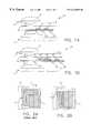
- FIG. 1Ais a cross sectional diagram of a pixel as envisioned by the present invention.
- FIG. 1Bis a cross sectional diagram of a second embodiment of the present invention.
- FIG. 2Ais a diagram of a typical prior art pixel for an Active Pixel Sensor
- FIG. 2Bis a diagram of a pixel for an Active Pixel Sensor as envisioned by the present invention.
- FIG. 3Ais an electrostatic diagram for the reset function of the present invention shown in FIG. 1A;
- FIG. 3Bis an electrostatic diagram for the reset function of the present invention shown in FIG. 1B;
- FIG. 4Ais an electrostatic diagram for the integration function of the present invention shown in FIG. 1A;
- FIG. 4Bis an electrostatic diagram for the integration function of the present invention shown in FIG. 1B;
- FIG. 5Ais an electrostatic diagram for the transfer function of the present invention shown in FIG. 1A;
- FIG. 5Bis an electrostatic diagram for the transfer function of the present invention shown in FIG. 1B;
- FIG. 6Ais an electrostatic diagram for the store function of the present invention shown in FIG. 1A.
- FIG. 6Bis an electrostatic diagram for the store function of the present invention shown in FIG. 1 B.
- This pixel architecture and method of operationeliminates the image artifacts caused by the line by line integration and read out method of prior art APS devices, while maintaining electronic shuttering capability and antiblooming control.
- FIG. 1 A and FIG. 1Billustrate cross sections of two different embodiments of the present invention illustrating relevant regions of the pixel architecture. While it will be understood to those skilled in the art that numerous variations of the specific physical embodiments of this invention can be achieved, these preferred embodiments are chosen for example and illustration.
- the photodetector shown in FIGS. 1A and 1B as a pinned photodiodecould be any photosensing means such as a photogate or photodiode that do not have pinning layers.
- the pixel in FIG. 1Acomprises a photodiode 12 with a vertical overflow drain 14 , transfer gate 16 , floating diffusion 18 , reset gate 17 , reset drain 19 , and a light shield 8 .
- a light shield aperture 9 , color filter 4 , and ⁇ Lens 6are placed over the photodetector such that light is focused through microlens 6 into light shield aperture 9 after passing through color filter 4 . Therefore, the light entering photodiode 12 has a wavelength that is within a predetermined bandwidth as determined by the color filter 4 .
- FIG. 1Bis a cross sectional diagram of a second embodiment of the present invention, and is similar in many respects to the embodiment shown in FIG. 1 a except that there are two transfer gates 26 , 36 , and a storage region 38 .
- the light shieldis constructed by effectively covering all regions except the photodetectors (photodiode 12 in this case), with an opaque layer or overlapping layers, so that incident light falls only on the photodiode area. Creation of an aperture in a light shield that limits the creation of photoelectrons to the photodetector region suppresses cross-talk between pixels.
- FIG. 2AA comparison of prior art APS pixels to the present invention is seen by comparing FIG. 2A to FIG. 2 B.
- the prior art device 5would simply pack the required active transistors into a region as small as possible, as indicated as amplifier area 25 , and then allocate the remaining pixel area to the photodetector area 15 , without regard to the resulting shape of the photodetector.
- the photodetectorlacked dimensional symmetry, and is not well suited for incorporation of CFA and ⁇ Lens.
- the present inventionemploys a symmetrically shaped photodetector area, seen here as rectangular photodetector area 11 , that is symmetric in 2-dimensions about its center.
- FIG. 2A and 2BWhile a rectangular photodetector is shown, a square, elliptical or circular shaped photodetector is also envisioned.
- the symmetry of the photodetectormakes possible an economical manner of placing light shield 8 , aperture 9 , color filter 4 and micro-lens 6 above the photodetector region. This provides the ability to make a pixel with the same fill factor as the prior art pixel, with a physically smaller pixel. Alternatively, one can keep the same pixel size and allocate a larger area to the amplifier, providing more amplifier design flexibility, and maintain the same fill factor as the prior art pixel. This can be seen in comparing FIGS. 2A and 2B. If one places a microlens over a prior art pixel as shown in FIG.
- the fill factor of the pixelis maximized.
- the microlensin order to focus the light into the area as shown, the microlens must be offset from the pixel center. Consequently, there is no longer any benefit to having photodetector area in the upper right hand corner of the pixel.
- the capacitance of the photodetectoris unnecessarily large. This will adversely affect the sensitivity in the case of a photodiode or photogate detector. It will also increase the amount of pixel cross-talk and reduce the latitude of color filter array overlap, producing a degradation in the MTF of the sensor.
- the fill factoris identical to that of the prior art pixel.
- the modificationcan be accomplished by keeping the pixel size the same and allocating more pixel area to the amplifier. This provides lower fixed pattern noise and 1/f noise.
- the modificationcan also be accomplished by simply eliminating the part of the photodetector in the upper right hand corner of the prior art pixel, thus reducing the size of the pixel. This provides a higher resolution sensor with the same fill factor.
- Prior art APS sensorsare typically monochrome, and their corresponding fabrication techniques did not elicit the type of architecture that lends itself to color pixel architecture. Additionally, prior art APS pixels did not provide a light shield within the pixel, and did not employ a microlens.
- FIG. 3Aillustrates the reset operation for the pixel 1 in FIG. 1 A.
- the pixel 10is reset by turning both Transfer Gate 16 and Reset Gate 17 on, as shown. Any electrons in the photodiode 12 , and floating diffusion 18 are pulled out through the reset drain 19 . This is done simultaneously at each pixel, and done once per frame.
- FIG. 3Billustrates the reset operation for the pixel 2 shown in FIG. 1B, where the pixel 20 is reset by turning on Transfer Gate 26 , Storage region 38 , Transfer Gate 36 and Reset Gate 27 .
- any electrons in the photodiode 12 , floating diffusion 28 , and storage region 38are pulled out through the reset drain 29 . Again, this is done simultaneously at each pixel, and done once per frame.
- FIG. 1Banother reset mode can be employed, by pulsing the VOD 14 (or turning on the lateral overflow drain (LOD) if used instead of a VOD). This empties the photodiode 12 only.
- the floating diffusion 28can then be reset on a line by line basis (as in prior art, except reset is done before read) so that a reset level can be stored and used for correlated double sampling.
- Image integrationis accomplished by collecting photo-generated electrons in the photodiode.
- the transfer gate 16is placed at a voltage that provides an electrostatic barrier between the photodiode and the floating diffusion (transfer gate 16 off state), and the reset gate 17 is held either in its on or off state (see FIG. 4 A).
- integrationis done with transfer gate 26 in the off state as shown in FIG. 4 B.
- the storage region 38 and transfer gate 36can be on or off, but preferably storage region 38 is kept in an off state to reduce cross-talk, see FIG. 4 B.
- reset gate 27 and transfer gate 36 on during this timewill eliminate dark current signal from building up in the floating diffusion 28 or storage region 38 , and allows long integration times.
- the integration timeis determined by the time between the photodetector reset and transfer (see transfer operation described below).
- chargeis transferred from the photodiode to the floating diffusion or storage region.
- thisis done by pulsing transfer gate 16 on (i.e. by making the electrostatic potential under transfer gate 16 deeper than the potential of photodiode 12 ).
- Reset gate 17must be turned off prior to transfer (see FIG. 5 A).
- transferis accomplished as shown in FIG. 5B, by pulsing transfer gate 26 on and turning storage region 38 on while keeping transfer gate 36 off.
- charge transferis done simultaneously at each pixel. Since the floating diffusion and storage region 38 regions are shielded from the scene illumination and are protected from blooming of charge in the photodiode, the signal can be stored on the floating diffusion or under the storage region without being modulated by the scene illumination.
- FIG. 6Awhich show the read operation for the device of FIG. 1A
- the chargeis already residing on the floating diffusion 18 , so the read operation is accomplished by simply addressing each pixel as done in prior art. In this case a reset level cannot be read line by line, thus it is not possible to perform correlated double sampling, as previously discussed.
- the read operationis accomplished by first resetting the floating diffusion by turning reset gate 27 on; next reading the reset level, then pulsing transfer gate 36 on while turning storage region 38 off. The charge has now been transferred to the floating diffusion, and the signal charge can be read.
- This architectureprovides the capability to do correlated double sampling. Refer to FIG. 6 B.
- Antiblooming control during integrationcan be accomplished in a similar manner to that of prior art APS devices. This is done by keeping the reset gate on during integration so that any excess photoelectrons generated in the photodetector can spill over the transfer gate onto the floating diffusion and be removed via the reset drain. This method cannot be used to provide antiblooming control during readout of prior art or present invention devices. If the incident image changes such that an extremely bright region appears during the readout period, excess photoelectrons will be generated in the short readout time and corrupt the signal electron packet that is being sensed on the floating diffusion. This will be more problematic in the present invention since the time of the storage operation can exceed the time of the readout operation. A new means for antiblooming control during readout and storage operation is thus required.
- Antibloomingis controlled by adjusting the electrostatic barrier to the VOD 14 such that it is deeper than the off potential for the transfer gate 16 for the case of FIG. 1A (or transfer gate 26 for the case of FIG. 1 B). This will allow excess electrons generated by any bright object in the scene to spill into the VOD 14 , and not bloom into the floating diffusion 18 (or floating diffusion 28 for the case of FIG. 1B) or other areas of the same pixel or adjacent pixels and cause undesired blooming artifacts.
- Antiblooming controlcan be done similarly with a lateral overflow drain (not shown), using either a physical gate or a virtual gate adjacent to the photodiode.
- the potential of the electrostatic barrier to the lateral overflow drain (LOD)must also be deeper than that of the transfer gate. This approach adversely affects the fill factor for a given pixel size since area must be allocated to the LOD structure.
- a VODprovides blooming control without impacting fill.
- Electronic shutteringrefers to the ability to shutter the imager without the need for a mechanical or electro-optic device to block the incident light. Electronic shuttering is accomplished by having a light shielded charge storage region in each pixel, (floating diffusion 18 in this case of FIG. 1A, storage region 38 for FIG. 11 B), and an overflow drain for the photodiode (VOD 14 in the case of the preferred embodiment being discussed, herein). As described in discussion relating to integration operation, the shutter or integration time is simply time between reset and transfer, or the time between turning off the LOD (or the VOD 14 ) and transfer.
- the LODis turned on by application of a signal pulse to the lateral overflow gate, or the VOD 14 is turned on by applying a signal pulse to the VOD 14 itself
- the chargeis transferred to light shielded floating diffusion ( 18 or 28 ) or storage region 38 , it can then be stored or read out without being affected by the incident light because electrons are now not photo-generated in the floating diffusion ( 18 or 28 ) or storage region 38 , and electrons generated in the photodiode during the storage and read out interval cannot spill over into the floating diffusion 18 or storage region 38 regions since they are taken out by the VOD 14 .
Landscapes
- Solid State Image Pick-Up Elements (AREA)
Abstract
Description
Claims (21)
Priority Applications (1)
| Application Number | Priority Date | Filing Date | Title |
|---|---|---|---|
| US09/448,375US6218692B1 (en) | 1999-11-23 | 1999-11-23 | Color active pixel sensor with electronic shuttering, anti-blooming and low cross talk |
Applications Claiming Priority (1)
| Application Number | Priority Date | Filing Date | Title |
|---|---|---|---|
| US09/448,375US6218692B1 (en) | 1999-11-23 | 1999-11-23 | Color active pixel sensor with electronic shuttering, anti-blooming and low cross talk |
Publications (1)
| Publication Number | Publication Date |
|---|---|
| US6218692B1true US6218692B1 (en) | 2001-04-17 |
Family
ID=23780066
Family Applications (1)
| Application Number | Title | Priority Date | Filing Date |
|---|---|---|---|
| US09/448,375Expired - LifetimeUS6218692B1 (en) | 1999-11-23 | 1999-11-23 | Color active pixel sensor with electronic shuttering, anti-blooming and low cross talk |
Country Status (1)
| Country | Link |
|---|---|
| US (1) | US6218692B1 (en) |
Cited By (12)
| Publication number | Priority date | Publication date | Assignee | Title |
|---|---|---|---|---|
| WO2001063905A3 (en)* | 2000-02-23 | 2002-05-30 | Photobit Corp | Frame shutter pixel with an isolated storage node |
| US20020063198A1 (en)* | 2000-10-26 | 2002-05-30 | Krymski Alexander I. | Frame shutter for CMOS APS |
| US20020109160A1 (en)* | 2001-01-15 | 2002-08-15 | Keiji Mabuchi | Solid-state image pickup device and driving method therefor |
| US6586283B2 (en)* | 2000-03-30 | 2003-07-01 | Agilent Technologies, Inc. | Apparatus and method for protecting integrated circuit charge storage elements from photo-induced currents |
| US20050029553A1 (en)* | 2003-08-04 | 2005-02-10 | Jaroslav Hynecek | Clocked barrier virtual phase charge coupled device image sensor |
| KR100486756B1 (en)* | 2001-11-01 | 2005-05-03 | 매그나칩 반도체 유한회사 | Method for fabrication of image sensor |
| US20060038203A1 (en)* | 2004-08-23 | 2006-02-23 | Eastman Kodak Company | Methods to eliminate amplifier glowing artifact in digital images captured by an image sensor |
| US20060044432A1 (en)* | 2004-08-27 | 2006-03-02 | Eastman Kodak Company | Fast flush structure for solid-state image sensors |
| US7091530B1 (en) | 2002-07-03 | 2006-08-15 | Massachusetts Institute Of Technology | High-speed, high-sensitivity charge-coupled device with independent pixel control of charge collection and storage |
| EP2821812A4 (en)* | 2012-02-28 | 2015-10-21 | Hamamatsu Photonics Kk | DISTANCE SENSOR AND IMAGE SENSOR |
| US9526468B2 (en) | 2014-09-09 | 2016-12-27 | General Electric Company | Multiple frame acquisition for exposure control in X-ray medical imagers |
| US20180269245A1 (en)* | 2015-09-17 | 2018-09-20 | Semiconductor Components Industries, Llc | High dynamic range pixel using light separation |
Citations (19)
| Publication number | Priority date | Publication date | Assignee | Title |
|---|---|---|---|---|
| US4373167A (en) | 1978-01-13 | 1983-02-08 | Tokyo Shibaura Denki Kabushiki Kaisha | Solid state image sensor with overflow protection and high resolution |
| US4467341A (en) | 1982-02-12 | 1984-08-21 | Tokyo Shibaura Denki Kabushiki Kaisha | Charge transfer imaging device with blooming overflow drain beneath transfer channel |
| US4696021A (en) | 1982-06-03 | 1987-09-22 | Nippon Kogaku K.K. | Solid-state area imaging device having interline transfer CCD means |
| US4928158A (en) | 1987-10-20 | 1990-05-22 | Mitsubishi Denki Kabushiki Kaisha | Solid-state image sensor having a plurality of horizontal transfer portions |
| US4958207A (en) | 1989-03-17 | 1990-09-18 | Loral Fairchild Corporation | Floating diode gain compression |
| US4977584A (en) | 1988-10-21 | 1990-12-11 | Nec Corporation | CCD image sensor with vertical overflow drain |
| US5028970A (en) | 1987-10-14 | 1991-07-02 | Fuji Photo Film Co., Ltd. | Image sensor |
| US5235197A (en) | 1991-06-25 | 1993-08-10 | Dalsa, Inc. | High photosensitivity and high speed wide dynamic range ccd image sensor |
| US5479049A (en) | 1993-02-01 | 1995-12-26 | Sharp Kabushiki Kaisha | Solid state image sensor provided with a transparent resin layer having water repellency and oil repellency and flattening a surface thereof |
| US5493143A (en) | 1993-07-23 | 1996-02-20 | Nec Corporation | Solid color image pickup device |
| US5631704A (en) | 1994-10-14 | 1997-05-20 | Lucent Technologies, Inc. | Active pixel sensor and imaging system having differential mode |
| US5739548A (en)* | 1995-05-02 | 1998-04-14 | Matsushita Electronics Corporation | Solid state imaging device having a flattening layer and optical lenses |
| US5789774A (en)* | 1996-03-01 | 1998-08-04 | Foveonics, Inc. | Active pixel sensor cell that minimizes leakage current |
| US5841158A (en)* | 1996-03-01 | 1998-11-24 | Foveonics, Inc. | Low-stress photodiode with reduced junction leakage |
| US5867215A (en)* | 1995-04-11 | 1999-02-02 | Eastman Kodak Company | Image sensor having multiple storage wells per pixel |
| US5880495A (en)* | 1998-01-08 | 1999-03-09 | Omnivision Technologies, Inc. | Active pixel with a pinned photodiode |
| US5892253A (en)* | 1997-03-26 | 1999-04-06 | Foveonics, Inc. | Active pixel sensor cell with balanced blue response and reduced noise |
| US5977576A (en)* | 1996-02-21 | 1999-11-02 | Sony Corporation | Image sensor |
| US5986297A (en)* | 1996-05-22 | 1999-11-16 | Eastman Kodak Company | Color active pixel sensor with electronic shuttering, anti-blooming and low cross-talk |
- 1999
- 1999-11-23USUS09/448,375patent/US6218692B1/ennot_activeExpired - Lifetime
Patent Citations (19)
| Publication number | Priority date | Publication date | Assignee | Title |
|---|---|---|---|---|
| US4373167A (en) | 1978-01-13 | 1983-02-08 | Tokyo Shibaura Denki Kabushiki Kaisha | Solid state image sensor with overflow protection and high resolution |
| US4467341A (en) | 1982-02-12 | 1984-08-21 | Tokyo Shibaura Denki Kabushiki Kaisha | Charge transfer imaging device with blooming overflow drain beneath transfer channel |
| US4696021A (en) | 1982-06-03 | 1987-09-22 | Nippon Kogaku K.K. | Solid-state area imaging device having interline transfer CCD means |
| US5028970A (en) | 1987-10-14 | 1991-07-02 | Fuji Photo Film Co., Ltd. | Image sensor |
| US4928158A (en) | 1987-10-20 | 1990-05-22 | Mitsubishi Denki Kabushiki Kaisha | Solid-state image sensor having a plurality of horizontal transfer portions |
| US4977584A (en) | 1988-10-21 | 1990-12-11 | Nec Corporation | CCD image sensor with vertical overflow drain |
| US4958207A (en) | 1989-03-17 | 1990-09-18 | Loral Fairchild Corporation | Floating diode gain compression |
| US5235197A (en) | 1991-06-25 | 1993-08-10 | Dalsa, Inc. | High photosensitivity and high speed wide dynamic range ccd image sensor |
| US5479049A (en) | 1993-02-01 | 1995-12-26 | Sharp Kabushiki Kaisha | Solid state image sensor provided with a transparent resin layer having water repellency and oil repellency and flattening a surface thereof |
| US5493143A (en) | 1993-07-23 | 1996-02-20 | Nec Corporation | Solid color image pickup device |
| US5631704A (en) | 1994-10-14 | 1997-05-20 | Lucent Technologies, Inc. | Active pixel sensor and imaging system having differential mode |
| US5867215A (en)* | 1995-04-11 | 1999-02-02 | Eastman Kodak Company | Image sensor having multiple storage wells per pixel |
| US5739548A (en)* | 1995-05-02 | 1998-04-14 | Matsushita Electronics Corporation | Solid state imaging device having a flattening layer and optical lenses |
| US5977576A (en)* | 1996-02-21 | 1999-11-02 | Sony Corporation | Image sensor |
| US5789774A (en)* | 1996-03-01 | 1998-08-04 | Foveonics, Inc. | Active pixel sensor cell that minimizes leakage current |
| US5841158A (en)* | 1996-03-01 | 1998-11-24 | Foveonics, Inc. | Low-stress photodiode with reduced junction leakage |
| US5986297A (en)* | 1996-05-22 | 1999-11-16 | Eastman Kodak Company | Color active pixel sensor with electronic shuttering, anti-blooming and low cross-talk |
| US5892253A (en)* | 1997-03-26 | 1999-04-06 | Foveonics, Inc. | Active pixel sensor cell with balanced blue response and reduced noise |
| US5880495A (en)* | 1998-01-08 | 1999-03-09 | Omnivision Technologies, Inc. | Active pixel with a pinned photodiode |
Non-Patent Citations (4)
| Title |
|---|
| "128x128 CMOS Photodiode-Type Active Pixel Sensor With On-Chip Timing, Control and Signal Chain Electronics", by R. H. Nixon et al., Proceedings of the SPIE, vol. 2415, "Charge-Coupled Devices and Solid-State Optical Sensors V", paper 34 (1995), pp. 1-7. |
| "Active Pixel Sensors: Are CCD's Dinosaurs?", Jul., 1993, by Eric R. Fossum, SPIE, vol. 1900-08-8194-1133,. |
| "Technology and Device Scaling Considerations For CMOS Imagers", by Hon-Sum Wong, IEEE Transactions On Electron Devices, vol. 43, No. 12, Dec. 1996, pp. 2131-2142. |
| "128×128 CMOS Photodiode-Type Active Pixel Sensor With On-Chip Timing, Control and Signal Chain Electronics", by R. H. Nixon et al., Proceedings of the SPIE, vol. 2415, "Charge-Coupled Devices and Solid-State Optical Sensors V", paper 34 (1995), pp. 1-7. |
Cited By (24)
| Publication number | Priority date | Publication date | Assignee | Title |
|---|---|---|---|---|
| US7687302B2 (en) | 2000-02-23 | 2010-03-30 | Aptina Imaging Corporation | Frame shutter pixel with an isolated storage node |
| WO2001063905A3 (en)* | 2000-02-23 | 2002-05-30 | Photobit Corp | Frame shutter pixel with an isolated storage node |
| US7388239B2 (en) | 2000-02-23 | 2008-06-17 | Micron Technology, Inc. | Frame shutter pixel with an isolated storage node |
| US20050077549A1 (en)* | 2000-02-23 | 2005-04-14 | Fossum Eric R. | Frame shutter pixel with an isolated storage node |
| US6624456B2 (en) | 2000-02-23 | 2003-09-23 | Micron Technology, Inc. | Frame shutter pixel with an isolated storage node |
| US6586283B2 (en)* | 2000-03-30 | 2003-07-01 | Agilent Technologies, Inc. | Apparatus and method for protecting integrated circuit charge storage elements from photo-induced currents |
| US20040227060A1 (en)* | 2000-10-26 | 2004-11-18 | Krymski Alexander I. | Frame shutter for CMOS APS |
| US20020063198A1 (en)* | 2000-10-26 | 2002-05-30 | Krymski Alexander I. | Frame shutter for CMOS APS |
| US7259790B2 (en)* | 2001-01-15 | 2007-08-21 | Sony Corporation | MOS type solid-state image pickup device and driving method comprised of a photodiode a detection portion and a transfer transistor |
| US7518168B2 (en) | 2001-01-15 | 2009-04-14 | Sony Corporation | MOS type solid-state image pickup device and driving method comprised of a photodiode, a detection portion, and a transfer transistor |
| US20020109160A1 (en)* | 2001-01-15 | 2002-08-15 | Keiji Mabuchi | Solid-state image pickup device and driving method therefor |
| US20070278533A1 (en)* | 2001-01-15 | 2007-12-06 | Sony Corporation | Mos type solid-state image pickup device and driving method comprised of a photodiode, a detection portion, and a tranfer transistor |
| KR100486756B1 (en)* | 2001-11-01 | 2005-05-03 | 매그나칩 반도체 유한회사 | Method for fabrication of image sensor |
| US7091530B1 (en) | 2002-07-03 | 2006-08-15 | Massachusetts Institute Of Technology | High-speed, high-sensitivity charge-coupled device with independent pixel control of charge collection and storage |
| EP1624492A3 (en)* | 2003-08-04 | 2006-06-07 | Texas Instruments Incorporated | Virtual phase charge coupled device image sensor |
| US20050029553A1 (en)* | 2003-08-04 | 2005-02-10 | Jaroslav Hynecek | Clocked barrier virtual phase charge coupled device image sensor |
| US7402882B2 (en)* | 2004-08-23 | 2008-07-22 | Eastman Kodak Company | Methods to eliminate amplifier glowing artifact in digital images captured by an image sensor |
| US20060038203A1 (en)* | 2004-08-23 | 2006-02-23 | Eastman Kodak Company | Methods to eliminate amplifier glowing artifact in digital images captured by an image sensor |
| US20060044432A1 (en)* | 2004-08-27 | 2006-03-02 | Eastman Kodak Company | Fast flush structure for solid-state image sensors |
| US7492404B2 (en) | 2004-08-27 | 2009-02-17 | Eastman Kodak Company | Fast flush structure for solid-state image sensors |
| EP2821812A4 (en)* | 2012-02-28 | 2015-10-21 | Hamamatsu Photonics Kk | DISTANCE SENSOR AND IMAGE SENSOR |
| US9526468B2 (en) | 2014-09-09 | 2016-12-27 | General Electric Company | Multiple frame acquisition for exposure control in X-ray medical imagers |
| US20180269245A1 (en)* | 2015-09-17 | 2018-09-20 | Semiconductor Components Industries, Llc | High dynamic range pixel using light separation |
| US10475832B2 (en)* | 2015-09-17 | 2019-11-12 | Semiconductor Components Industries, Llc | High dynamic range pixel using light separation |
Similar Documents
| Publication | Publication Date | Title |
|---|---|---|
| US5986297A (en) | Color active pixel sensor with electronic shuttering, anti-blooming and low cross-talk | |
| US6943838B2 (en) | Active pixel sensor pixel having a photodetector whose output is coupled to an output transistor gate | |
| KR100331995B1 (en) | Arrangement of circuits in pixels, each circuit shared by a plurality of pixels, in image sensing apparatus | |
| US10536652B2 (en) | Image sensors with split photodiodes | |
| US8228411B2 (en) | Circuit and photo sensor overlap for backside illumination image sensor | |
| US8723284B1 (en) | Back side illuminated CMOS image sensor with global shutter storage gates stacked on top of pinned photodiodes | |
| US6218656B1 (en) | Photodiode active pixel sensor with shared reset signal row select | |
| US8878264B2 (en) | Global shutter pixel with improved efficiency | |
| US6624850B1 (en) | Photogate active pixel sensor with high fill factor and correlated double sampling | |
| US8928792B1 (en) | CMOS image sensor with global shutter, rolling shutter, and a variable conversion gain, having pixels employing several BCMD transistors coupled to a single photodiode and dual gate BCMD transistors for charge storage and sensing | |
| US20050128327A1 (en) | Device and method for image sensing | |
| JP2001203940A (en) | Image sensor | |
| US20010032983A1 (en) | Solid state imaging apparatus, method of manufacturing the same and video system using such solid state imaging apparatus | |
| CN110113546A (en) | The combination of adjacent pixel unit and reading method in imaging system and pixel array | |
| JP2011216970A (en) | Solid-state imaging apparatus, method of driving the same and electronic device | |
| JP4727045B2 (en) | Analog storage device for CMOS array | |
| US20110139963A1 (en) | Image sensors, methods, and pixels with storage and transfer gates | |
| US6218692B1 (en) | Color active pixel sensor with electronic shuttering, anti-blooming and low cross talk | |
| JP7520493B2 (en) | Image pickup device, its manufacturing method, and image pickup apparatus | |
| US20240214707A1 (en) | Solid-state imaging device, method for manufacturing solid-state imaging device, and electronic apparatus | |
| JPH05137072A (en) | Solid-state imaging device | |
| JP3919243B2 (en) | Photoelectric conversion device | |
| US20100181465A1 (en) | Snapshot mode active pixel sensor | |
| JPH05175471A (en) | Solid-state image sensing device | |
| JP3466660B2 (en) | Solid-state imaging device |
Legal Events
| Date | Code | Title | Description |
|---|---|---|---|
| AS | Assignment | Owner name:EASTMAN KODAK COMPANY, NEW YORK Free format text:ASSIGNMENT OF ASSIGNORS INTEREST;ASSIGNORS:GUIDASH, ROBERT M.;LEE, PAUL P.;LEE, TEH-HSUANG;REEL/FRAME:010653/0225;SIGNING DATES FROM 20000121 TO 20000210 | |
| STCF | Information on status: patent grant | Free format text:PATENTED CASE | |
| FEPP | Fee payment procedure | Free format text:PAYOR NUMBER ASSIGNED (ORIGINAL EVENT CODE: ASPN); ENTITY STATUS OF PATENT OWNER: LARGE ENTITY | |
| FPAY | Fee payment | Year of fee payment:4 | |
| FPAY | Fee payment | Year of fee payment:8 | |
| AS | Assignment | Owner name:OMNIVISION TECHNOLOGIES, INC., CALIFORNIA Free format text:ASSIGNMENT OF ASSIGNORS INTEREST;ASSIGNOR:EASTMAN KODAK COMPANY;REEL/FRAME:026227/0213 Effective date:20110415 | |
| FEPP | Fee payment procedure | Free format text:PAYOR NUMBER ASSIGNED (ORIGINAL EVENT CODE: ASPN); ENTITY STATUS OF PATENT OWNER: LARGE ENTITY Free format text:PAYER NUMBER DE-ASSIGNED (ORIGINAL EVENT CODE: RMPN); ENTITY STATUS OF PATENT OWNER: LARGE ENTITY | |
| FPAY | Fee payment | Year of fee payment:12 |