US6218680B1 - Semi-insulating silicon carbide without vanadium domination - Google Patents
Semi-insulating silicon carbide without vanadium dominationDownload PDFInfo
- Publication number
- US6218680B1 US6218680B1US09/313,802US31380299AUS6218680B1US 6218680 B1US6218680 B1US 6218680B1US 31380299 AUS31380299 AUS 31380299AUS 6218680 B1US6218680 B1US 6218680B1
- Authority
- US
- United States
- Prior art keywords
- silicon carbide
- single crystal
- concentration
- carbide single
- vanadium
- Prior art date
- Legal status (The legal status is an assumption and is not a legal conclusion. Google has not performed a legal analysis and makes no representation as to the accuracy of the status listed.)
- Expired - Lifetime
Links
Images


Classifications
- C—CHEMISTRY; METALLURGY
- C30—CRYSTAL GROWTH
- C30B—SINGLE-CRYSTAL GROWTH; UNIDIRECTIONAL SOLIDIFICATION OF EUTECTIC MATERIAL OR UNIDIRECTIONAL DEMIXING OF EUTECTOID MATERIAL; REFINING BY ZONE-MELTING OF MATERIAL; PRODUCTION OF A HOMOGENEOUS POLYCRYSTALLINE MATERIAL WITH DEFINED STRUCTURE; SINGLE CRYSTALS OR HOMOGENEOUS POLYCRYSTALLINE MATERIAL WITH DEFINED STRUCTURE; AFTER-TREATMENT OF SINGLE CRYSTALS OR A HOMOGENEOUS POLYCRYSTALLINE MATERIAL WITH DEFINED STRUCTURE; APPARATUS THEREFOR
- C30B23/00—Single-crystal growth by condensing evaporated or sublimed materials
- C—CHEMISTRY; METALLURGY
- C30—CRYSTAL GROWTH
- C30B—SINGLE-CRYSTAL GROWTH; UNIDIRECTIONAL SOLIDIFICATION OF EUTECTIC MATERIAL OR UNIDIRECTIONAL DEMIXING OF EUTECTOID MATERIAL; REFINING BY ZONE-MELTING OF MATERIAL; PRODUCTION OF A HOMOGENEOUS POLYCRYSTALLINE MATERIAL WITH DEFINED STRUCTURE; SINGLE CRYSTALS OR HOMOGENEOUS POLYCRYSTALLINE MATERIAL WITH DEFINED STRUCTURE; AFTER-TREATMENT OF SINGLE CRYSTALS OR A HOMOGENEOUS POLYCRYSTALLINE MATERIAL WITH DEFINED STRUCTURE; APPARATUS THEREFOR
- C30B29/00—Single crystals or homogeneous polycrystalline material with defined structure characterised by the material or by their shape
- C30B29/10—Inorganic compounds or compositions
- C30B29/36—Carbides
- C—CHEMISTRY; METALLURGY
- C30—CRYSTAL GROWTH
- C30B—SINGLE-CRYSTAL GROWTH; UNIDIRECTIONAL SOLIDIFICATION OF EUTECTIC MATERIAL OR UNIDIRECTIONAL DEMIXING OF EUTECTOID MATERIAL; REFINING BY ZONE-MELTING OF MATERIAL; PRODUCTION OF A HOMOGENEOUS POLYCRYSTALLINE MATERIAL WITH DEFINED STRUCTURE; SINGLE CRYSTALS OR HOMOGENEOUS POLYCRYSTALLINE MATERIAL WITH DEFINED STRUCTURE; AFTER-TREATMENT OF SINGLE CRYSTALS OR A HOMOGENEOUS POLYCRYSTALLINE MATERIAL WITH DEFINED STRUCTURE; APPARATUS THEREFOR
- C30B33/00—After-treatment of single crystals or homogeneous polycrystalline material with defined structure
Definitions
- the present inventionrelates to the growth of high quality silicon carbide crystals for specific purposes, and in particular relates to the production of high quality semi-insulating silicon carbide substrates that are useful in microwave devices.
- This inventionwas made under Department of the Air Force Contract Number F33615-95-C-5426. The government may have certain rights in this invention.
- microwavesrefers to electromagnetic energy in frequencies covering the range of about 0.1 gigahertz (GHz) to 1,000 GHz with corresponding wavelengths from about 300 centimeters to about 0.3 millimeters.
- GHzgigahertz
- microwavesare perhaps most widely associated by the layperson with cooking devices, those persons familiar with electronic devices recognize that the microwave frequencies are used for a large variety of electronic purposes and in corresponding electronic devices, including various communication devices, and the associated circuit elements and circuits that operate them.
- the ability of a device (or circuit) to exhibit certain desired or necessary performance characteristicsdepends to a large extent, and often entirely, upon the material from which it is made.
- silicon carbidewhich offers a primary advantage for microwave applications of a very high electric breakdown field. This characteristic of silicon carbide enables devices such as metal semiconductor field effect transistors (MESFETs) to operate at drain voltages ten times higher than field effect transistors formed in gallium arsenide (GaAs).
- MOSFETsmetal semiconductor field effect transistors
- silicon carbidehas the significant advantage of a thermal conductivity of 4.9 watts per degree Kelvin per centimeter (W/K-cm) which is 3.3 times higher than silicon and ten times higher than either gallium arsenide or sapphire. These properties give silicon carbide a high power density in terms of gate periphery measured in terms of watts per millimeter (W/mm) and also an extremely high power handling capability in terms of die area (W/mm). This is particularly advantageous for high power, high frequency applications because die size becomes limited by wavelength. Accordingly, because of the excellent thermal and electronic properties of silicon carbide, at any given frequency, silicon carbide MESFETs should be capable of at least five times the power of devices made from gallium arsenide.
- high resistivityAs recognized by those familiar with microwave devices, they often require high resistivity (“semi-insulating”) substrates for coupling purposes because conductive substrates tend to cause significant problems at microwave frequencies.
- high resistivityand “semi-insulating” can be considered synonymous for most purposes. In general, both terms describe a semiconductor material having a resistivity greater than about 1500 ohm-centimeters ( ⁇ -cm).
- microwave devicesare particularly important for monolithic microwave integrated circuits (MMICs) which are widely used in communications devices such as pagers and cellular phones, and which generally require a high resistivity substrate. Accordingly, the following characteristics are desirable for microwave device substrates: A high crystalline quality suitable for highly complex, high performance circuit elements, good thermal conductivity, good electrical isolation between devices and to the substrate, low resistive loss characteristics, low cross-talk characteristics, and large wafer diameter.
- silicon carbideWith silicon carbide's wide bandgap (3.2 eV in 4H silicon carbide at 300K), such semi-insulating characteristics should be theoretically possible. As one result, an appropriate high resistivity silicon carbide substrate would permit both power and passive devices to be placed on the same integrated circuit (“chip”) thus decreasing the size of the device while increasing its efficiency and performance. Silicon carbide also provides other favorable qualities, including the capacity to operate at high temperatures without physical, chemical, or electrical breakdown.
- silicon carbide grown by most techniquesis generally too conductive for these purposes.
- the nominal or unintentional nitrogen concentration in silicon carbidetends to be high enough in sublimation grown crystals (1-2 ⁇ 10 17 cm ⁇ 3 ) to provide sufficient conductivity to prevent such silicon carbide from being used in microwave devices.
- silicon carbide devicesshould have a substrate resistivity of at least 1500 ohm-centimeters ( ⁇ -cm) in order to achieve RF passive behavior. Furthermore, resistivities of 5000 ⁇ -cm or better are needed to minimize device transmission line losses to an acceptable level of 0.1 dB/cm or less. For device isolation and to minimize backgating effects, the resistivity of semi-insulating silicon carbide should approach a range of 50,000 ⁇ -cm or higher.
- the deep levels in the silicon carbide between the valence and conduction bandscan be produced by the controlled introduction of selected elements such as transition metals or passivating elements such as hydrogen, chlorine or fluorine, or combinations of these elements into the silicon carbide to form the deep level centers in the silicon carbide; e.g., column 3, lines 37-53.
- selected elementssuch as transition metals or passivating elements such as hydrogen, chlorine or fluorine, or combinations of these elements
- passivating elementssuch as hydrogen, chlorine or fluorine, or combinations of these elements
- these deep level elemental impuritiescan be incorporated by introducing them during high temperature sublimation or chemical vapor deposition (CVD) growth of high purity silicon carbide.
- vanadiumis considered a desirable transition metal for this purpose. According to the '955 patent and similar art, the vanadium compensates the silicon carbide material and produces the high resistivity (i.e., semi-insulating) characteristics of silicon carbide.
- vanadiumas a compensating element to produce semi-insulating silicon carbide, however, also introduces certain disadvantages.
- the presence of electronically significant amounts of any dopant, including vanadiumcan negatively affect the crystalline quality of the resulting material. Accordingly, to the extent that vanadium or other elements can be significantly reduced or eliminated, the crystal quality of the resulting material, and its corresponding electronic quality, can be increased.
- compensating amounts of vanadiumcan cause growth defects such as inclusions and micropipes in silicon carbide.
- the introduction of compensating amounts of vanadiumcan reduce the yield and add expense to the production of semi-insulating silicon carbide substrates.
- the proactive compensation of silicon carbide, or any other semiconductor elementcan be somewhat complex and unpredictable and thus introduces manufacturing complexity that can be desirably avoided if the compensation can be avoided.
- the inventionmeets this object with a semi-insulating bulk single crystal of silicon carbide having a resistivity of at least 5000 ⁇ -cm at room temperature and a concentration of deep level trapping elements that is below detectable levels or that does not affect the electronic properties of the material.
- the inventionis a method of producing a semi-insulating bulk single crystal of silicon carbide.
- the methodcomprises heating a silicon carbide source powder to sublimation while heating and then maintaining a silicon carbide seed crystal to a temperature below the temperature of the source powder at which temperature sublimed species from the source powder will condense upon the seed crystal; and continuing to heat the silicon carbide source powder until a desired amount of single crystal bulk growth has occurred upon the seed crystal.
- the methodis characterized in that the amounts of deep level trapping elements in the source powder are below detectable levels; and in that during sublimation growth, the source powder and the seed crystal are maintained at respective temperatures high enough to significantly reduce the amount of nitrogen that would otherwise be incorporated into the bulk growth on the seed crystal and to increase the number of point defects in the bulk growth to an amount that renders the resulting silicon carbide bulk single crystal semi-insulating.
- the inventioncomprises devices that incorporate the semi-insulating silicon carbide according to the claimed invention, including MSFETs, certain MOSFETs, and HEMTs (High Electron Mobility Transistors).
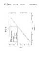
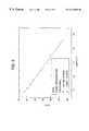
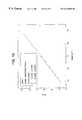
- FIGS. 1 through 3are the plots of the Hall effect measurements carried out on wafers made according to the present invention.
- FIG. 4is a plot of the natural log of the carrier concentration against the reciprocal temperature (degrees Kelvin) for semi-insulating silicon carbide according to the present invention.
- FIG. 5is a plot of the natural log of the resistivity as against reciprocal temperature for semi-insulating silicon carbide according to the present invention.
- FIGS. 6 through 8are the same measurements as represented in FIGS. 1 through 3, but taken from a different portion of the substrate wafer;
- FIG. 9is another plot of the natural log that carrier concentration versus reciprocal temperature for the samples illustrated in FIGS. 6 through 8;
- FIG. 10is another plot of the natural log of resistivity versus reciprocal temperature and again corresponding to the sample measurements of FIGS. 6 through 8;
- FIGS. 11 through 13are yet another set of plots identical to FIGS. 1 through 3 and 6 through 8 for yet another measurement on a different portion of the semi-conducting silicon carbide material;
- FIG. 14is another plot of the natural log of resistivity as against reciprocal temperature for the samples illustrated in FIGS. 11 through 13;
- FIGS. 15, 16 , and 17are plots of Secondary Ion Mass Spectroscopy (SIMS) for various samples of materials according to the present invention and prior art material.
- SIMSSecondary Ion Mass Spectroscopy
- the inventionis a semi-insulating bulk single crystal of silicon carbide having concentration of deep level trapping elements that is below a level at which such elements dominate the resistivity of the crystal and preferably at a concentration that is below detectable levels.
- deep level trapping elementrefers to those elements from the periodic table which, when incorporated as dopants in silicon carbide form states at levels between the valence and conduction bands of silicon carbide that are much farther removed (i.e., at least 300 MeV) from both the conduction and valence bands than are more conventional p-type or n-type dopants.
- common deep level trapping elementsinclude vanadium and other transition metals.
- the concentration that is defined as “below detectable levels,”refers to elements that are present in amounts that cannot be detected by modern sophisticated analytical techniques.
- the detectable limits referred to hereinare those amounts of elements such as vanadium and other transition metals that are present in amounts of less than 1 ⁇ 10 16 cm ⁇ 3 (1E16), or in other cases, less than about 1E14. These two amounts represent typical detection limits for most trace elements (particularly vanadium) using SIMS techniques; e.g., SIMS Theory—Sensitivity and Detection Limits, Charles Evans & Associates (1995), www.cea.com.
- vanadium (V)is one of the more common elements for producing deep level traps in silicon carbide. Accordingly, the invention is characterized in that vanadium is either absent, or if present, is present in amounts below those which will substantially affect the resistivity of the crystal, and preferably below the amount that can be detected by SIMS.
- the silicon carbide single crystal according to this embodiment of the inventionpreferably has a polytype selected from the group consisting of the 3C, 4H, 6H and 15R polytypes.
- silicon carbide single crystals according to this embodiment of the inventionpreferably have a concentration of nitrogen atoms below about 1 ⁇ 10 17 cm ⁇ 3 (1E17). More preferably, the silicon carbide semi-insulating single crystal according to the present invention will have a concentration of nitrogen of 5E16 or less. Because the concentration of vanadium is below the level that affects the electrical characteristics of the crystal, and preferably less than can be detected by secondary ion mass spectroscopy, the concentration of vanadium is accordingly less than 1E16 atoms per cubic centimeter, and most preferably less than 1E14 atoms per cubic centimeter. Additionally, the resulting bulk silicon carbide single crystal will preferably have a resistivity of at least 10,000 ⁇ -cm at room temperature, and most preferably a resistivity of at least 50,000 ⁇ -cm at room temperature.
- the 4H polytypeis preferred for, its higher bulk electron mobility.
- the other polytypesmay be preferred.
- one of the more preferred embodiments of the inventionis a semi-insulating bulk single crystal of 4H silicon carbide that has a resistivity of at least 10,000 ⁇ -cm at room temperature and concentration of vanadium atoms of less than 1E14.
- the inventioncomprises a method of producing a semi-insulating bulk single crystal of silicon carbide.
- the methodcomprises heating a silicon carbide source powder to sublimation while, heating and then maintaining a silicon carbide seed crystal to a temperature below the temperature of the source powder, and at which temperature sublimed species from the source powder will condense upon the seed crystal. Thereafter, the method includes continuing to heat the silicon carbide source powder until a desired amount of single crystal bulk growth has occurred upon the seed crystal.
- the methodis characterized in that (1) the amounts of deep level trapping elements in the source powder (as described above) are below the relevant amounts, (2) the source powder contains 5E16 or less nitrogen, and (3) during sublimation growth, the source powder and the seed crystal are maintained at respective temperatures high enough to significantly reduce the amount of nitrogen that would otherwise be incorporated into the bulk growth on the seed crystal and to increase the number of point defects (sometimes referred to as intrinsic point defects) in the bulk growth on the seed crystal to an amount that renders the resulting silicon carbide bulk single crystal semi-insulating.
- the number of point defects required to make the crystal semi-insulatingcan also be minimized.
- the preferred number of point defectsappears to be in the range of 1E15-5E17.
- the resulting deep traps in the silicon carbide that render it semi-insulatingappear to result from vacancies, interstitials or other intrinsic point defects rather than the presence of vanadium, other transition metals, or other elements.
- the source powder that is usedmust be free of vanadium, or if vanadium is present, it must be below detectable levels.
- the detectable levelsare typically characterized as those that can be measured using SIMS.
- the amount of vanadium in the source powderis preferably less than 1E16 atoms per cubic centimeter, and most preferably less than 1E14 atoms per cubic centimeter.
- the amount of nitrogen in the resulting bulk single crystalcan be reduced, not only by using the high purity techniques referred to in the prior art (which are certainly acceptable as part of the inventive technique), but also by carrying out the sublimation at relatively higher temperatures, while keeping the temperature of the seed crystal, and any bulk growth on the seed crystal at a temperature below the temperature of the source powder.
- a preferred technique for sublimation growthis set forth in U.S. Pat. No. Re. 34,861, the contents of which are incorporated entirely herein by reference (“the '861 patent”).
- the sublimationis carried out in an appropriate crucible that, as set forth in the '861 patent, is typically formed of graphite.
- the crucibleincludes a seed holder, and both are positioned inside of a sublimation furnace.
- the SiC source powderis selected and purified as necessary to have a nitrogen concentration of less than about 1E17 and preferably less than about 5E16.
- the source powderhas a concentration of vanadium, or other heavy metals or transition elements, that is below the amount that would affect the electrical characteristics of the resulting crystal.
- Such amountsinclude those below SIMS-detectable levels, meaning that using currently available SIMS, they are at least below 1E16 and preferably below 1E14 atoms per cubic centimeter.
- the source powderalso preferably meets the other advantageous characteristics set forth in the '861 patent.
- silicon carbide sublimationcan be carried out with source temperatures ranging from about 2100° C. to 2500° C. with the temperature of the seed crystal being kept proportionally lower.
- the sourcewas kept at between about 2360 and 2380° C. with the seed being 300-350° C. lower.
- the indicated temperaturescan depend on how and where the system is measured and may differ slightly from system to system.
- vanadiumhas been the deep level trapping element of choice for prior attempts to produce compensated-type semi-insulating silicon carbide
- the inventioncan be expressed as the bulk SiC single crystal, and the method of making it, in which vanadium is below the detectable and numerical levels recited above. It will be understood, however, by those familiar with the growth of silicon carbide and the characteristics of silicon carbide as used for semiconductor purposes, however, that the invention likewise contemplates the absence of any other elements which would produce deep level traps.
- the inventionBy avoiding the use of elements to create the deep level traps, the invention likewise eliminates the need to compensate the trapping elements with other elements and correspondingly reduces the complications that such compensation introduces into the crystal growth processes.
- FIGS. 1 through 17illustrate various measurements carried out on the semi-insulating substrates according to the present invention, along with some comparisons with more conventional compensated and uncompensated silicon carbide material.
- FIGS. 1 through 3represent a corresponding set of measurements taken on a substrate wafer grown at Cree Research Inc., Durham, N.C., in accordance with the present invention. As set forth in the “Experimental” portion herein, the characteristics of these materials were tested by the Air Force Research Laboratory in Dayton, Ohio.
- FIG. 1plots the carrier concentration as against reciprocal temperature (with the concentration being on a logarithmic scale) for a semi-insulating substrate wafer according to the present invention. The slope of the resulting line gives the activation energy which is approximately 1.1 electron volts (eV).
- FIG. 2shows that the resistivity increases as the temperature decreases in a manner consistent with the other expected properties of the semi-insulating material according to the present invention.
- FIG. 3represents the mobility plotted against the temperature in degrees Kelvin.
- FIG. 4is a plot of the natural logarithm (ln) of the carrier concentration plotted against reciprocal temperature (degrees Kelvin). As known to those familiar with these measurements, the slope of the natural log of the carrier concentration against reciprocal temperature gives the activation energy. As indicated by the inset box in FIG. 4, the activation energy for this sample according to the invention is on the order of 1.1 eV, i.e., consistent with the results in FIG. 1 . By comparison, and as likewise known to those familiar with semi-insulating silicon carbide, the activation energy for the semi-insulating silicon carbide when vanadium is used as the deep level trapping element would be about 1.6 eV under the same circumstances.
- the datawas measured under a magnetic field of 4 kilogauss on a sample thickness of 0.045 centimeters and over a temperature range from about 569 K to about 1,012 K.
- FIG. 5is a plot of the natural log of resistivity as against reciprocal temperature in degrees Kelvin. This data and this plot can likewise be used to determine the activation energy of the semi-insulating silicon carbide material. The value of 1.05667 eV determined from this plot helps confirm the 1.1 eV activation energy measured earlier. Stated differently, the difference between the activation energies as measured in FIGS. 4 and 5 is within expected experimental limits, and the data confirm each other.
- FIGS. 6 through 10represent the same types of measurements and plots as do FIGS. 1 through 5, but taken from a different sample; specifically a different area of the same wafer as that measured for FIGS. 1 through 5. It will accordingly be seen that FIGS. 6 through 8 are consistent with the results plotted in FIGS. 1 through 3. More specifically, FIG. 9, which is another plot of the natural log of carrier concentration against reciprocal temperature, shows a calculated activation energy of 1.00227 eV. Again, this is within experimental limits of the 1.1 eV measured earlier.
- FIG. 10plots the natural log of resistivity against the reciprocal temperature and similarly provides an activation energy of 1.01159, which likewise is within experimental limits of 1.1 eV.
- FIGS. 11 through 13show results from yet another portion of the wafer, but which are considered less favorable than the results seen in the prior measurements. In particular, the plot of FIG. 11 fails to form a straight line in the manner desired, and the data is less favorable than were the earlier results.
- FIG. 14, which plots the natural log of resistivity against reciprocal temperatureshows a calculated activation energy of only 0.63299, a value well removed from 1.1 eV, regardless of the experimental uncertainty.
- FIGS. 15, 16 , and 17represent the secondary ion mass spectra (SIMS) of various comparative samples and tend to show the elemental impurities and other materials in the semi-insulating silicon carbide substrates.
- FIG. 15is the SIMS spectra of the semi-insulating silicon carbide material according to the present invention and confirms the absence of vanadium or any other transition metals in the sample. This confirms that the activation energy and deep level states present in the invention do not result from the presence of vanadium or other transition metals.
- FIG. 16is included for comparison purposes and is the SIMS spectrum of an N-type wafer of silicon carbide that is neither semi-insulating nor made according to the present invention, but instead represents a conductive silicon carbide sample. Because no reason exists to include vanadium for N-type substrates, vanadium is absent from the mass spectrum.
- FIG. 17provides a comparison of a prior version of semi-insulating silicon carbide which is compensated with vanadium.
- the vanadium peakis strongly present at approximately 51 atomic mass units in the spectrum. This vanadium peak is conspicuously absent from both FIGS. 15 and 16.
- the inventioncomprises a semi-insulating silicon carbide single crystal with shallow donor dopants, shallow acceptor dopants, and intrinsic point defects.
- the number of shallow donor dopants (N d ) in the silicon carbide crystalis greater than the number of shallow acceptor dopants (N a ), and the number of intrinsic point defects (N d1 ) in the silicon carbide that act as acceptors is greater than the numerical difference between the number of these donor and acceptor dopants.
- the concentration of elements selected from the group consisting of transition elements and heavy metalsis less than the concentration that would affect the electrical properties of the silicon carbide single crystal.
- the resulting silicon carbide single crystalhas a resistivity of at least 5000 ⁇ -cm at room temperature.
- This aspect of the inventionalso applies to the complementary situation in which the number of acceptor dopant atoms is greater than the number of donor dopant atoms.
- the number of intrinsic point defects that act as donorsis greater than the numerical difference between the number of the shallow donor impurities and the shallow acceptor impurities.
- the shallow n-type and p-type dopantscompensate each other with one or the other predominating to a certain extent.
- the number of intrinsic point defects in the crystal that are electrically activatedis greater than the net amount of n-type or p-type dopant atoms that predominate over the other in the crystal. Stated as a formula,
- acceptorspredominate over donors.
- the crystalwould be compensated n-type based on dopant atoms. These net donors are compensated again, however, by acceptor-type point defects to produce the semi-insulating crystal.
- the point defectsact as donor type and compensate the net excess of acceptors in the crystal.
- the term “dopant”is used in a broad sense; i.e., to describe an atom other than silicon (Si) or carbon (C) present in the crystal lattice and providing either an extra electron (a donor) or an extra hole (an acceptor).
- the dopantscan be present either passively or proactively; i.e., the term “dopant” implies neither a “doping” step nor the absence of one.
- the number of point defectscan be controlled to some extent by irradiating silicon carbide with neutrons, high energy electrons, or gamma rays to create the desired number of point defects to achieve the results consistent with the formulas set forth above.
- EPRelectron paramagnetic resonance
- DLTSdeep level transient spectroscopy
- position annihilation spectroscopygive the best available indications of the numbers present.
- Hall effect measurementsalso confirm the desired characteristics of the crystal.
- the inventioncan be incorporated into active devices, particularly active microwave devices, that take advantage of the semi-insulating silicon carbide substrate.
- active devicesparticularly active microwave devices, that take advantage of the semi-insulating silicon carbide substrate.
- the frequency with which a microwave device can operatecan be significantly hindered by any interaction of carriers with the substrate, as opposed to the ideal situation when the carriers are limited to a particular channel and other functional portions of the microwave device.
- the nature of the silicon carbide semi-insulating material according to the present inventionis such that it has excellent performance characteristics in the appropriate devices. These include, but are not limited to MESFETs, certain MOSFETS, and other devices such as those described in current U.S. patents and pending applications Nos. 5,270,554; 5,686,737; 5,719,409; 5,831,288; Ser. No. 08/891,221, filed Jul. 10, 1997; and Ser. No. 09/082,554, filed May 21, 1998, both for “Latch-up Free Power UMOS Bipolar Transistor”; Ser. No. 08/797,536, filed Feb. 7, 1997 for “Structure for Increasing the Maximum Voltage of Silicon Carbide Power Transistors”; Ser. No.
- Both waferswere insulating at room temperature.
- the measurable waferwas thermally activated at elevated temperatures and the carrier concentration was measurable, which is not always possible in semi-insulating material because of the low mobilities due to the high temperatures involved.
- the carrier concentrationwas around 10 15 cm ⁇ 3 at 1000K where the resistivity was about 103 ⁇ -cm. Such carrier concentration is about one to two orders of magnitude lower than that seen in conventional semi-insulating material or vanadium doped material at the same temperature. No fit of the n vs 1/T curve could be made, however, so the total concentration for the active layer remained unavailable.
- the activation energywas around 1.1 eV.
- FIGS. 18-20The mass scan for the invention along with the scans for two comparative samples are included herewith as FIGS. 18-20, respectively. Titanium (Ti) is apparent at around 1 ⁇ 10 16 cm ⁇ 3 in FIGS. 19 and 20, but not in the sample of the invention (FIG. 18 ). Vanadium also appears in the standard semi-insulating sample FIG. 20) along with the SiOH line indicating hydrogen.
- the first waferwas considered to be very high purity material, and is considered insulating because any residual vanadium impurities along with what other defect makes up the 1.1 eV level are present in concentrations larger than the sum of the shallow impurities and so the 1.1 eV levels compensates the shallow impurities.
- the Fermi levelis pinned at the deep level, thus making the material semi-insulating.
- the presence of hydrogen, if any,could mean that hydrogen compensation is taking place, but such would not be expected to selectively compensate or neutralize the shallow impurities and not the deep levels.
Landscapes
- Chemical & Material Sciences (AREA)
- Engineering & Computer Science (AREA)
- Crystallography & Structural Chemistry (AREA)
- Materials Engineering (AREA)
- Metallurgy (AREA)
- Organic Chemistry (AREA)
- Inorganic Chemistry (AREA)
- Crystals, And After-Treatments Of Crystals (AREA)
- Junction Field-Effect Transistors (AREA)
- Inorganic Insulating Materials (AREA)
- Ceramic Products (AREA)
Abstract
Description
The present invention relates to the growth of high quality silicon carbide crystals for specific purposes, and in particular relates to the production of high quality semi-insulating silicon carbide substrates that are useful in microwave devices. This invention was made under Department of the Air Force Contract Number F33615-95-C-5426. The government may have certain rights in this invention.
The term “microwaves” refers to electromagnetic energy in frequencies covering the range of about 0.1 gigahertz (GHz) to 1,000 GHz with corresponding wavelengths from about 300 centimeters to about 0.3 millimeters. Although “microwaves” are perhaps most widely associated by the layperson with cooking devices, those persons familiar with electronic devices recognize that the microwave frequencies are used for a large variety of electronic purposes and in corresponding electronic devices, including various communication devices, and the associated circuit elements and circuits that operate them. As is the case with many other semiconductor electronic devices and resulting circuits, the ability of a device (or circuit) to exhibit certain desired or necessary performance characteristics depends to a large extent, and often entirely, upon the material from which it is made. One appropriate candidate material for microwave devices is silicon carbide, which offers a primary advantage for microwave applications of a very high electric breakdown field. This characteristic of silicon carbide enables devices such as metal semiconductor field effect transistors (MESFETs) to operate at drain voltages ten times higher than field effect transistors formed in gallium arsenide (GaAs).
Additionally, silicon carbide has the significant advantage of a thermal conductivity of 4.9 watts per degree Kelvin per centimeter (W/K-cm) which is 3.3 times higher than silicon and ten times higher than either gallium arsenide or sapphire. These properties give silicon carbide a high power density in terms of gate periphery measured in terms of watts per millimeter (W/mm) and also an extremely high power handling capability in terms of die area (W/mm). This is particularly advantageous for high power, high frequency applications because die size becomes limited by wavelength. Accordingly, because of the excellent thermal and electronic properties of silicon carbide, at any given frequency, silicon carbide MESFETs should be capable of at least five times the power of devices made from gallium arsenide.
As recognized by those familiar with microwave devices, they often require high resistivity (“semi-insulating”) substrates for coupling purposes because conductive substrates tend to cause significant problems at microwave frequencies. As used herein, the terms “high resistivity” and “semi-insulating” can be considered synonymous for most purposes. In general, both terms describe a semiconductor material having a resistivity greater than about 1500 ohm-centimeters (Ω-cm).
Such microwave devices are particularly important for monolithic microwave integrated circuits (MMICs) which are widely used in communications devices such as pagers and cellular phones, and which generally require a high resistivity substrate. Accordingly, the following characteristics are desirable for microwave device substrates: A high crystalline quality suitable for highly complex, high performance circuit elements, good thermal conductivity, good electrical isolation between devices and to the substrate, low resistive loss characteristics, low cross-talk characteristics, and large wafer diameter.
Given silicon carbide's wide bandgap (3.2 eV in 4H silicon carbide at 300K), such semi-insulating characteristics should be theoretically possible. As one result, an appropriate high resistivity silicon carbide substrate would permit both power and passive devices to be placed on the same integrated circuit (“chip”) thus decreasing the size of the device while increasing its efficiency and performance. Silicon carbide also provides other favorable qualities, including the capacity to operate at high temperatures without physical, chemical, or electrical breakdown.
As those familiar with silicon carbide are aware, however, silicon carbide grown by most techniques is generally too conductive for these purposes. In particular, the nominal or unintentional nitrogen concentration in silicon carbide tends to be high enough in sublimation grown crystals (1-2×1017cm−3) to provide sufficient conductivity to prevent such silicon carbide from being used in microwave devices.
Some recent efforts have attempted to compensate the effective level of nitrogen by adding a p-type (i.e., acceptor) dopant such as boron. In practice, however, SiC-based devices made using boron to obtain high resistivity have exhibited unexpectedly poor results at high power levels. Additionally, in comparison to some other elements, boron tends to diffuse relatively well in SiC, giving it an undesirable tendency to migrate into adjacent device layers and unintentionally affect them.
In order to be particularly useful, silicon carbide devices should have a substrate resistivity of at least 1500 ohm-centimeters (Ω-cm) in order to achieve RF passive behavior. Furthermore, resistivities of 5000 Ω-cm or better are needed to minimize device transmission line losses to an acceptable level of 0.1 dB/cm or less. For device isolation and to minimize backgating effects, the resistivity of semi-insulating silicon carbide should approach a range of 50,000 Ω-cm or higher. Present work tends to assert that the semi-insulating behavior of a silicon carbide substrate is the result of energy levels deep within the band gap of the silicon carbide; i.e., farther from both the valence band and the conduction band than the energy levels created by p-type and n-type dopants. These “deep” energy levels are believed to consist of states lying at least 300 meV away from the conduction or valence band edges, e.g., U.S. Pat. No. 5,611,955 which is representative of current conventional thinking in this art. According to the '955 patent, the deep levels in the silicon carbide between the valence and conduction bands can be produced by the controlled introduction of selected elements such as transition metals or passivating elements such as hydrogen, chlorine or fluorine, or combinations of these elements into the silicon carbide to form the deep level centers in the silicon carbide; e.g., column 3, lines 37-53. See also, Mitchel, The 1.1 eV Deep Level in 4H-SiC. SIMC-X, Berkley Calif., June 1998; Hobgood, Semi-Insulating GH-SiC Grown by Physical Vapor Transport, Appl. Phys. Lett. Vol. 66, No. 11 (1995); WO 95/04171; Sriram, RF Performance of SiC MESFETs on High Resistivity Substrates, IEEE Electron Device Letters, Vol. 15, No. 11 (1994); Evwaraye, Examination of Electrical and Optical Properties of Vanadium in Bulk n-type Silicon Carbide, J. Appl. Phys. 76 (10) (1994); Schneider, Infrared Spectra and Electron Spin Resonance of Vanadium Deep Level Impurities in Silicon Carbide, Appl. Phys. Lett. 56(12) (1990); and Allen, Frequency and Power Performance of Microwave SiC FET's, Proceedings of International Conference on Silicon Carbide and Related Materials 1995, Institute of Physics.
Further to the conventional thinking, these deep level elemental impurities (also known as deep level trapping elements) can be incorporated by introducing them during high temperature sublimation or chemical vapor deposition (CVD) growth of high purity silicon carbide. In particular, vanadium is considered a desirable transition metal for this purpose. According to the '955 patent and similar art, the vanadium compensates the silicon carbide material and produces the high resistivity (i.e., semi-insulating) characteristics of silicon carbide.
The introduction of vanadium as a compensating element to produce semi-insulating silicon carbide, however, also introduces certain disadvantages. First, the presence of electronically significant amounts of any dopant, including vanadium, can negatively affect the crystalline quality of the resulting material. Accordingly, to the extent that vanadium or other elements can be significantly reduced or eliminated, the crystal quality of the resulting material, and its corresponding electronic quality, can be increased. In particular, the present understanding is that compensating amounts of vanadium can cause growth defects such as inclusions and micropipes in silicon carbide.
As a second disadvantage, the introduction of compensating amounts of vanadium can reduce the yield and add expense to the production of semi-insulating silicon carbide substrates. Third, the proactive compensation of silicon carbide, or any other semiconductor element, can be somewhat complex and unpredictable and thus introduces manufacturing complexity that can be desirably avoided if the compensation can be avoided.
Therefore, it is an object of the present invention to provide a semi-insulating silicon carbide substrate that offers the capabilities that are required and advantageous for high frequency operation, but while avoiding the disadvantages of prior materials and techniques.
The invention meets this object with a semi-insulating bulk single crystal of silicon carbide having a resistivity of at least 5000 Ω-cm at room temperature and a concentration of deep level trapping elements that is below detectable levels or that does not affect the electronic properties of the material.
In another aspect, the invention is a method of producing a semi-insulating bulk single crystal of silicon carbide. The method comprises heating a silicon carbide source powder to sublimation while heating and then maintaining a silicon carbide seed crystal to a temperature below the temperature of the source powder at which temperature sublimed species from the source powder will condense upon the seed crystal; and continuing to heat the silicon carbide source powder until a desired amount of single crystal bulk growth has occurred upon the seed crystal. The method is characterized in that the amounts of deep level trapping elements in the source powder are below detectable levels; and in that during sublimation growth, the source powder and the seed crystal are maintained at respective temperatures high enough to significantly reduce the amount of nitrogen that would otherwise be incorporated into the bulk growth on the seed crystal and to increase the number of point defects in the bulk growth to an amount that renders the resulting silicon carbide bulk single crystal semi-insulating.
In yet another aspect, the invention comprises devices that incorporate the semi-insulating silicon carbide according to the claimed invention, including MSFETs, certain MOSFETs, and HEMTs (High Electron Mobility Transistors).
The foregoing and other objects and advantages of the invention and the manner in which the same are accomplished will become clearer based on the following detailed description taken in conjunction with the accompanying drawings in which:
FIGS. 1 through 3 are the plots of the Hall effect measurements carried out on wafers made according to the present invention.
FIG. 4 is a plot of the natural log of the carrier concentration against the reciprocal temperature (degrees Kelvin) for semi-insulating silicon carbide according to the present invention.
FIG. 5 is a plot of the natural log of the resistivity as against reciprocal temperature for semi-insulating silicon carbide according to the present invention;
FIGS. 6 through 8 are the same measurements as represented in FIGS. 1 through 3, but taken from a different portion of the substrate wafer;
FIG. 9 is another plot of the natural log that carrier concentration versus reciprocal temperature for the samples illustrated in FIGS. 6 through 8;
FIG. 10 is another plot of the natural log of resistivity versus reciprocal temperature and again corresponding to the sample measurements of FIGS. 6 through 8;
FIGS. 11 through 13 are yet another set of plots identical to FIGS. 1 through 3 and6 through8 for yet another measurement on a different portion of the semi-conducting silicon carbide material;
FIG. 14 is another plot of the natural log of resistivity as against reciprocal temperature for the samples illustrated in FIGS. 11 through 13; and
FIGS. 15,16, and17 are plots of Secondary Ion Mass Spectroscopy (SIMS) for various samples of materials according to the present invention and prior art material.
In a first embodiment, the invention is a semi-insulating bulk single crystal of silicon carbide having concentration of deep level trapping elements that is below a level at which such elements dominate the resistivity of the crystal and preferably at a concentration that is below detectable levels.
As used herein the term “deep level trapping element” refers to those elements from the periodic table which, when incorporated as dopants in silicon carbide form states at levels between the valence and conduction bands of silicon carbide that are much farther removed (i.e., at least 300 MeV) from both the conduction and valence bands than are more conventional p-type or n-type dopants. As set forth in the Field and Background, common deep level trapping elements include vanadium and other transition metals.
As further used herein, the concentration that is defined as “below detectable levels,” refers to elements that are present in amounts that cannot be detected by modern sophisticated analytical techniques. In particular, because one of the more common techniques for detecting elements in small amounts is secondary ion mass spectroscopy (“SIMS”), the detectable limits referred to herein are those amounts of elements such as vanadium and other transition metals that are present in amounts of less than 1×1016cm−3(1E16), or in other cases, less than about 1E14. These two amounts represent typical detection limits for most trace elements (particularly vanadium) using SIMS techniques; e.g., SIMS Theory—Sensitivity and Detection Limits, Charles Evans & Associates (1995), www.cea.com.
As noted above, vanadium (V) is one of the more common elements for producing deep level traps in silicon carbide. Accordingly, the invention is characterized in that vanadium is either absent, or if present, is present in amounts below those which will substantially affect the resistivity of the crystal, and preferably below the amount that can be detected by SIMS.
Although other polytypes (ie., crystal structures) are possible, the silicon carbide single crystal according to this embodiment of the invention preferably has a polytype selected from the group consisting of the 3C, 4H, 6H and 15R polytypes.
Furthermore, in order to avoid the problems associated with the presence of nitrogen, and the resulting necessity to attempt to compensate for the nitrogen, silicon carbide single crystals according to this embodiment of the invention preferably have a concentration of nitrogen atoms below about 1×1017cm−3(1E17). More preferably, the silicon carbide semi-insulating single crystal according to the present invention will have a concentration of nitrogen of 5E16 or less. Because the concentration of vanadium is below the level that affects the electrical characteristics of the crystal, and preferably less than can be detected by secondary ion mass spectroscopy, the concentration of vanadium is accordingly less than 1E16 atoms per cubic centimeter, and most preferably less than 1E14 atoms per cubic centimeter. Additionally, the resulting bulk silicon carbide single crystal will preferably have a resistivity of at least 10,000 Ω-cm at room temperature, and most preferably a resistivity of at least 50,000 Ω-cm at room temperature.
For purposes of providing semi-insulating silicon carbide substrates for high frequency MESFETs, the 4H polytype is preferred for, its higher bulk electron mobility. For other devices, the other polytypes may be preferred. Accordingly, one of the more preferred embodiments of the invention is a semi-insulating bulk single crystal of 4H silicon carbide that has a resistivity of at least 10,000 Ω-cm at room temperature and concentration of vanadium atoms of less than 1E14.
In another embodiment, the invention comprises a method of producing a semi-insulating bulk single crystal of silicon carbide. In this embodiment, the method comprises heating a silicon carbide source powder to sublimation while, heating and then maintaining a silicon carbide seed crystal to a temperature below the temperature of the source powder, and at which temperature sublimed species from the source powder will condense upon the seed crystal. Thereafter, the method includes continuing to heat the silicon carbide source powder until a desired amount of single crystal bulk growth has occurred upon the seed crystal. The method is characterized in that (1) the amounts of deep level trapping elements in the source powder (as described above) are below the relevant amounts, (2) the source powder contains 5E16 or less nitrogen, and (3) during sublimation growth, the source powder and the seed crystal are maintained at respective temperatures high enough to significantly reduce the amount of nitrogen that would otherwise be incorporated into the bulk growth on the seed crystal and to increase the number of point defects (sometimes referred to as intrinsic point defects) in the bulk growth on the seed crystal to an amount that renders the resulting silicon carbide bulk single crystal semi-insulating. Preferably and conceptually, by keeping the amounts of nitrogen or other dopants as low as possible, the number of point defects required to make the crystal semi-insulating can also be minimized. Presently, the preferred number of point defects appears to be in the range of 1E15-5E17.
Although the inventors do not wish to be bound by any particular theory, the resulting deep traps in the silicon carbide that render it semi-insulating appear to result from vacancies, interstitials or other intrinsic point defects rather than the presence of vanadium, other transition metals, or other elements. In order to produce the semi-insulating silicon carbide according to the invention, the source powder that is used must be free of vanadium, or if vanadium is present, it must be below detectable levels. As noted above, the detectable levels are typically characterized as those that can be measured using SIMS. Stated differently, the amount of vanadium in the source powder is preferably less than 1E16 atoms per cubic centimeter, and most preferably less than 1E14 atoms per cubic centimeter.
It has been further discovered according to the present invention that the amount of nitrogen in the resulting bulk single crystal can be reduced, not only by using the high purity techniques referred to in the prior art (which are certainly acceptable as part of the inventive technique), but also by carrying out the sublimation at relatively higher temperatures, while keeping the temperature of the seed crystal, and any bulk growth on the seed crystal at a temperature below the temperature of the source powder. A preferred technique for sublimation growth (other than as modified as described herein) is set forth in U.S. Pat. No. Re. 34,861, the contents of which are incorporated entirely herein by reference (“the '861 patent”).
The sublimation is carried out in an appropriate crucible that, as set forth in the '861 patent, is typically formed of graphite. The crucible includes a seed holder, and both are positioned inside of a sublimation furnace. In the method of the present invention, the SiC source powder is selected and purified as necessary to have a nitrogen concentration of less than about 1E17 and preferably less than about 5E16. Furthermore, the source powder has a concentration of vanadium, or other heavy metals or transition elements, that is below the amount that would affect the electrical characteristics of the resulting crystal. Such amounts include those below SIMS-detectable levels, meaning that using currently available SIMS, they are at least below 1E16 and preferably below 1E14 atoms per cubic centimeter. The source powder also preferably meets the other advantageous characteristics set forth in the '861 patent.
From a practical standpoint, silicon carbide sublimation can be carried out with source temperatures ranging from about 2100° C. to 2500° C. with the temperature of the seed crystal being kept proportionally lower. For the materials described herein, the source was kept at between about 2360 and 2380° C. with the seed being 300-350° C. lower. As known to those familiar with such procedures and measurements, the indicated temperatures can depend on how and where the system is measured and may differ slightly from system to system.
Because vanadium has been the deep level trapping element of choice for prior attempts to produce compensated-type semi-insulating silicon carbide, the invention can be expressed as the bulk SiC single crystal, and the method of making it, in which vanadium is below the detectable and numerical levels recited above. It will be understood, however, by those familiar with the growth of silicon carbide and the characteristics of silicon carbide as used for semiconductor purposes, however, that the invention likewise contemplates the absence of any other elements which would produce deep level traps.
By avoiding the use of elements to create the deep level traps, the invention likewise eliminates the need to compensate the trapping elements with other elements and correspondingly reduces the complications that such compensation introduces into the crystal growth processes.
FIGS. 1 through 17 illustrate various measurements carried out on the semi-insulating substrates according to the present invention, along with some comparisons with more conventional compensated and uncompensated silicon carbide material.
FIGS. 1 through 3 represent a corresponding set of measurements taken on a substrate wafer grown at Cree Research Inc., Durham, N.C., in accordance with the present invention. As set forth in the “Experimental” portion herein, the characteristics of these materials were tested by the Air Force Research Laboratory in Dayton, Ohio. FIG. 1 plots the carrier concentration as against reciprocal temperature (with the concentration being on a logarithmic scale) for a semi-insulating substrate wafer according to the present invention. The slope of the resulting line gives the activation energy which is approximately 1.1 electron volts (eV).
FIG. 2 shows that the resistivity increases as the temperature decreases in a manner consistent with the other expected properties of the semi-insulating material according to the present invention.
FIG. 3 represents the mobility plotted against the temperature in degrees Kelvin. FIG. 4 is a plot of the natural logarithm (ln) of the carrier concentration plotted against reciprocal temperature (degrees Kelvin). As known to those familiar with these measurements, the slope of the natural log of the carrier concentration against reciprocal temperature gives the activation energy. As indicated by the inset box in FIG. 4, the activation energy for this sample according to the invention is on the order of 1.1 eV, i.e., consistent with the results in FIG.1. By comparison, and as likewise known to those familiar with semi-insulating silicon carbide, the activation energy for the semi-insulating silicon carbide when vanadium is used as the deep level trapping element would be about 1.6 eV under the same circumstances.
The data was measured under a magnetic field of 4 kilogauss on a sample thickness of 0.045 centimeters and over a temperature range from about 569 K to about 1,012 K.
FIG. 5 is a plot of the natural log of resistivity as against reciprocal temperature in degrees Kelvin. This data and this plot can likewise be used to determine the activation energy of the semi-insulating silicon carbide material. The value of 1.05667 eV determined from this plot helps confirm the 1.1 eV activation energy measured earlier. Stated differently, the difference between the activation energies as measured in FIGS. 4 and 5 is within expected experimental limits, and the data confirm each other.
FIGS. 6 through 10 represent the same types of measurements and plots as do FIGS. 1 through 5, but taken from a different sample; specifically a different area of the same wafer as that measured for FIGS. 1 through 5. It will accordingly be seen that FIGS. 6 through 8 are consistent with the results plotted in FIGS. 1 through 3. More specifically, FIG. 9, which is another plot of the natural log of carrier concentration against reciprocal temperature, shows a calculated activation energy of 1.00227 eV. Again, this is within experimental limits of the 1.1 eV measured earlier.
In a similar manner, FIG. 10 plots the natural log of resistivity against the reciprocal temperature and similarly provides an activation energy of 1.01159, which likewise is within experimental limits of 1.1 eV. FIGS. 11 through 13 show results from yet another portion of the wafer, but which are considered less favorable than the results seen in the prior measurements. In particular, the plot of FIG. 11 fails to form a straight line in the manner desired, and the data is less favorable than were the earlier results. Similarly, FIG. 14, which plots the natural log of resistivity against reciprocal temperature shows a calculated activation energy of only 0.63299, a value well removed from 1.1 eV, regardless of the experimental uncertainty.
FIGS. 15,16, and17 represent the secondary ion mass spectra (SIMS) of various comparative samples and tend to show the elemental impurities and other materials in the semi-insulating silicon carbide substrates. FIG. 15 is the SIMS spectra of the semi-insulating silicon carbide material according to the present invention and confirms the absence of vanadium or any other transition metals in the sample. This confirms that the activation energy and deep level states present in the invention do not result from the presence of vanadium or other transition metals.
FIG. 16 is included for comparison purposes and is the SIMS spectrum of an N-type wafer of silicon carbide that is neither semi-insulating nor made according to the present invention, but instead represents a conductive silicon carbide sample. Because no reason exists to include vanadium for N-type substrates, vanadium is absent from the mass spectrum.
FIG. 17 provides a comparison of a prior version of semi-insulating silicon carbide which is compensated with vanadium. The vanadium peak is strongly present at approximately 51 atomic mass units in the spectrum. This vanadium peak is conspicuously absent from both FIGS. 15 and 16.
It will be understood, of course, by those familiar with these materials, that although the phrase “below detectable amounts,” is an entirely appropriate description of the invention, these amounts can also be understood as those that are below the amount that affects the electronic characteristics, and particularly the resistivity, of the silicon carbide crystal.
Accordingly, in another aspect, the invention comprises a semi-insulating silicon carbide single crystal with shallow donor dopants, shallow acceptor dopants, and intrinsic point defects. In this aspect of the invention, the number of shallow donor dopants (Nd) in the silicon carbide crystal is greater than the number of shallow acceptor dopants (Na), and the number of intrinsic point defects (Nd1) in the silicon carbide that act as acceptors is greater than the numerical difference between the number of these donor and acceptor dopants. Further to this aspect, the concentration of elements selected from the group consisting of transition elements and heavy metals is less than the concentration that would affect the electrical properties of the silicon carbide single crystal. The resulting silicon carbide single crystal has a resistivity of at least 5000 Ω-cm at room temperature.
This aspect of the invention also applies to the complementary situation in which the number of acceptor dopant atoms is greater than the number of donor dopant atoms. In such a case, the number of intrinsic point defects that act as donors is greater than the numerical difference between the number of the shallow donor impurities and the shallow acceptor impurities.
Stated differently, the shallow n-type and p-type dopants compensate each other with one or the other predominating to a certain extent. The number of intrinsic point defects in the crystal that are electrically activated is greater than the net amount of n-type or p-type dopant atoms that predominate over the other in the crystal. Stated as a formula,
Nd1>(Nd−Na)
where donors predominate over acceptors, or
where acceptors predominate over donors. In the first case, the crystal would be compensated n-type based on dopant atoms. These net donors are compensated again, however, by acceptor-type point defects to produce the semi-insulating crystal. In the second case, the point defects act as donor type and compensate the net excess of acceptors in the crystal.
As used herein, the term “dopant” is used in a broad sense; i.e., to describe an atom other than silicon (Si) or carbon (C) present in the crystal lattice and providing either an extra electron (a donor) or an extra hole (an acceptor). In the invention, the dopants can be present either passively or proactively; i.e., the term “dopant” implies neither a “doping” step nor the absence of one.
It is expected that the number of point defects can be controlled to some extent by irradiating silicon carbide with neutrons, high energy electrons, or gamma rays to create the desired number of point defects to achieve the results consistent with the formulas set forth above.
Although an exact number of point defects is difficult to measure, techniques such as electron paramagnetic resonance (EPR), deep level transient spectroscopy (DLTS), and position annihilation spectroscopy give the best available indications of the numbers present. As further set forth herein, Hall effect measurements also confirm the desired characteristics of the crystal.
In another aspect, the invention can be incorporated into active devices, particularly active microwave devices, that take advantage of the semi-insulating silicon carbide substrate. As noted above and as recognized by those familiar with active semiconductor microwave devices, the frequency with which a microwave device can operate can be significantly hindered by any interaction of carriers with the substrate, as opposed to the ideal situation when the carriers are limited to a particular channel and other functional portions of the microwave device.
The nature of the silicon carbide semi-insulating material according to the present invention is such that it has excellent performance characteristics in the appropriate devices. These include, but are not limited to MESFETs, certain MOSFETS, and other devices such as those described in current U.S. patents and pending applications Nos. 5,270,554; 5,686,737; 5,719,409; 5,831,288; Ser. No. 08/891,221, filed Jul. 10, 1997; and Ser. No. 09/082,554, filed May 21, 1998, both for “Latch-up Free Power UMOS Bipolar Transistor”; Ser. No. 08/797,536, filed Feb. 7, 1997 for “Structure for Increasing the Maximum Voltage of Silicon Carbide Power Transistors”; Ser. No. 08/795,135, filed Feb. 7, 1997 for “Structure to Reduce the On-resistance of Power Transistors”; and International Application. No. PCT/US98/13003, filed Jun. 23, 1998 (designating the United States), for “Power Devices in Wide Bandgap Semiconductors”; the contents of all of which are incorporated entirely herein by reference.
Two wafers of semi-insulating SiC were examined at the Air Force Research Laboratory at Dayton, Ohio (Wright-Patterson Air Force Base), with high temperature Hall effect and SIMS. No understandable results were available from one of the wafers (possibly because of unsatisfactory ohmic contacts), but two Hall samples from the second wafer both gave the same results, giving a reasonable confidence level in those results.
Both wafers were insulating at room temperature. The measurable wafer was thermally activated at elevated temperatures and the carrier concentration was measurable, which is not always possible in semi-insulating material because of the low mobilities due to the high temperatures involved. The carrier concentration was around 1015cm−3at 1000K where the resistivity was about 103 Ω-cm. Such carrier concentration is about one to two orders of magnitude lower than that seen in conventional semi-insulating material or vanadium doped material at the same temperature. No fit of the n vs 1/T curve could be made, however, so the total concentration for the active layer remained unavailable. The activation energy was around 1.1 eV.
SIMS was carried out on the sample with a high resolution system. Nothing was seen other than some copper near the detection limit along with some hydrogen, which was surmised from the height of the mass 47 peak. The mass 47 peak was accordingly attributed to SiOH. The mass scan for the invention along with the scans for two comparative samples are included herewith as FIGS. 18-20, respectively. Titanium (Ti) is apparent at around 1×1016cm−3in FIGS. 19 and 20, but not in the sample of the invention (FIG.18). Vanadium also appears in the standard semi-insulating sample FIG. 20) along with the SiOH line indicating hydrogen.
From these results, the first wafer was considered to be very high purity material, and is considered insulating because any residual vanadium impurities along with what other defect makes up the 1.1 eV level are present in concentrations larger than the sum of the shallow impurities and so the 1.1 eV levels compensates the shallow impurities. The Fermi level is pinned at the deep level, thus making the material semi-insulating. The presence of hydrogen, if any, could mean that hydrogen compensation is taking place, but such would not be expected to selectively compensate or neutralize the shallow impurities and not the deep levels.
In the drawings and specification, there have been disclosed typical embodiments of the invention, and, although specific terms have been employed, they have been used in a generic and descriptive sense only and not for purposes of limitation, the scope of the invention being set forth in the following claims.
Claims (36)
1. A semi-insulating silicon carbide single crystal comprising:
shallow donor dopants, shallow acceptor dopants, and intrinsic point defects in said silicon carbide single crystal;
wherein the number of shallow dopants of a first conductivity type is greater than the number of shallow dopants of a second conductivity type; and
the number of intrinsic point defects in said silicon carbide crystal that act to compensate the predominating first type dopant is greater than the numerical difference by which said first type of shallow dopant predominates over said second type of shallow dopant; and
the concentration of elements selected from the group consisting of transition elements and heavy metals is less than the concentration that would affect the electrical properties of the silicon carbide single crystal;
said silicon carbide single crystal having a resistivity of at least 5000 ohm-cm at room temperature.
2. A semi-insulating silicon carbide crystal according to claim1 wherein said first type dopants are donors, said second type dopants are acceptors and said intrinsic point defects act as acceptors.
3. A semi-insulating silicon carbide crystal according to claim1 wherein said first type dopants are acceptors, said second type dopants are donors and said intrinsic point defects act as donors.
4. A silicon carbide single crystal according to claim1 wherein the polytype of the silicon carbide is selected from the group consisting of the 3C, 4H, 6H and 15R polytypes.
5. A silicon carbide single crystal according to claim1 wherein the concentration of nitrogen is 5×1016cm−3or less.
6. A silicon carbide single crystal according to claim1 wherein the concentration of vanadium is below the level that can be detected by secondary ion mass spectroscopy (SIMS).
7. A silicon carbide single crystal according to claim1 wherein the concentration of vanadium is less than 1×1014cm−3.
8. A silicon carbide single crystal according to claim1 having a resistivity of at least 10,000 Ω-cm at room temperature.
9. A silicon carbide single crystal according to claim1 having a resistivity of at least 50,000 Ω-cm at room temperature.
10. A transistor having a substrate that comprises the bulk single crystal according to claim1.
11. A transistor according to claim10 selected from the group consisting of: metal-semiconductor field-effect transistors, metal-insulator field effect transistors, and high electron mobility transistors.
12. A method of producing a semi-insulating bulk single crystal of silicon carbide, the method comprising:
heating a silicon carbide source powder in which the amounts of deep level trapping elements in the source powder are below detectable levels to sublimation while,
heating and then maintaining a silicon carbide seed crystal to a temperature below the temperature of the source powder at which temperature sublimed species from the source powder will condense upon the seed crystal; and
continuing to heat the silicon carbide source powder until a desired amount of single crystal bulk growth has occurred upon the seed crystal; and while
maintaining the source powder and the seed crystal during sublimation growth at respective temperatures high enough to significantly reduce the amount of nitrogen that would otherwise be incorporated into the bulk growth on the seed crystal and to increase the number of point defects in the bulk growth to an amount that renders the resulting silicon carbide bulk single crystal semi-insulating.
13. A method according to claim12 in which the amount of vanadium in the source powder is below detectable levels.
14. A method according to claim12 in which the amount of vanadium in the source powder is less than 1×1016cm−3.
15. A method according to claim12 in which the amount of vanadium in the source powder is less than 1×1014cm−3.
16. A method according to claim12 in which the concentration of transition metals in the source powder is less than 1×1014cm−3.
17. A semi-insulating silicon carbide single crystal having a concentration of nitrogen atoms of 5×1016cm−3or less and a concentration of point defects greater than the concentration of nitrogen but less than the concentration of point defects that begins to substantially reduce the thermal conductivity and other desirable properties of the crystal.
18. A semi-insulating bulk single crystal of silicon carbide according to claim17 having a resistivity of at least 5000 Ω-cm at room temperature and a concentration of deep level trapping elements that is below the amount that affects the electrical characteristics of the crystal.
19. A silicon carbide single crystal according to claim17 wherein the polytype of the silicon carbide is selected from the group consisting of the 3C, 4H, 6H and 15R polytypes.
20. A silicon carbide single crystal according to claim17 wherein the concentration of deep level trapping elements is below the level that can be detected by secondary ion mass spectroscopy (SIMS).
21. A silicon carbide single crystal according to claim17 wherein the concentration of vanadium is below the level that can be detected by secondary ion mass spectroscopy (SIMS).
22. A silicon carbide single crystal according to claim17 wherein the concentration of vanadium is less than 1×1016cm−3.
23. A silicon carbide single crystal according to claim17 wherein the concentration of vanadium is less than 1×1014cm−3.
24. A silicon carbide single crystal according to claim17 having a resistivity of at least 10,000 Ω-cm at room temperature.
25. A silicon carbide single crystal according to claim17 having a resistivity of at least 50,000 Ω-cm at room temperature.
26. A semi-insulating silicon carbide single crystal according to claim17 wherein the concentration of point defects does not exceed 5×1017cm−3.
27. A transistor having a substrate that comprises the bulk single crystal according to claim17.
28. A transistor according to claim27 selected from the group consisting of: metal-semiconductor field-effect transistors, metal-insulator field effect transistors, and high electron mobility transistors.
29. A method of producing a high resistivity silicon carbide single crystal substrate comprising:
irradiating a single crystal of silicon carbide,
in which the concentration of deep level trapping elements is below the amount that would affect the electrical properties of said silicon carbide single crystal,
with an irradiating source selected from the group consisting of neutrons, electrons, and gamma radiation, and
until the number of compensating point defects in the crystal is greater than the net amount of dopant atoms of one conductivity type that predominate over the dopant atoms of the other conductivity type in the crystal.
30. A method according to claim29 comprising irradiating a silicon carbide single wherein the polytype of the silicon carbide is selected from the group consisting of the 3C, 4H, 6H and 15R polytypes.
31. A method according to claim29 comprising irradiating a silicon carbide single crystal having a concentration of nitrogen atoms below 1×1017cm−3.
32. A method according to claim29 comprising irradiating A silicon carbide single crystal according to claim1 wherein the concentration of nitrogen is 5×1016cm−3or less.
33. A method according to claim29 comprising irradiating a silicon carbide single crystal wherein the concentration of deep level trapping elements is below the level that can be detected by secondary ion mass spectroscopy (SIMS).
34. A method according to claim29 comprising irradiating a silicon carbide single crystal wherein the concentration of vanadium is below the level that can be detected by secondary ion mass spectroscopy (SIMS).
35. A method according to claim29 comprising irradiating a silicon carbide single crystal wherein the concentration of vanadium is less than 1×1016cm−3.
36. A method according to claim29 comprising irradiating a silicon carbide single crystal wherein the concentration of vanadium is less than 1×1014cm−3.
Priority Applications (16)
| Application Number | Priority Date | Filing Date | Title |
|---|---|---|---|
| US09/313,802US6218680B1 (en) | 1999-05-18 | 1999-05-18 | Semi-insulating silicon carbide without vanadium domination |
| DE60030851TDE60030851T2 (en) | 1999-05-18 | 2000-05-17 | SILICON CARBIDE HALF-INSULATING NOT BY VANADIUM DOMINATED SILICON CARBIDE |
| AT00959134TATE340280T1 (en) | 1999-05-18 | 2000-05-17 | SEMI-INSULATION SILICON CARBIDE NOT DOMINATED BY VANADIUM |
| PCT/US2000/013557WO2000071787A2 (en) | 1999-05-18 | 2000-05-17 | Semi-insulating silicon carbide without vanadium domination |
| CA002376564ACA2376564C (en) | 1999-05-18 | 2000-05-17 | Semi-insulating silicon carbide without vanadium domination |
| CNB008077061ACN1222642C (en) | 1999-05-18 | 2000-05-17 | Semi-insulating silicon carbide without vandium dumination |
| AU70506/00AAU7050600A (en) | 1999-05-18 | 2000-05-17 | Semi-insulating silicon carbide without vanadium domination |
| EP00959134AEP1181401B1 (en) | 1999-05-18 | 2000-05-17 | Semi-insulating silicon carbide without vanadium domination |
| KR1020017013950AKR100767382B1 (en) | 1999-05-18 | 2000-05-17 | Semi-insulating silicon carbide without vanadium |
| ES00959134TES2272317T3 (en) | 1999-05-18 | 2000-05-17 | SEMIAISLANTE SILICON CARBIDE WITHOUT VANADIO DOMAIN. |
| JP2000620157AJP4860825B2 (en) | 1999-05-18 | 2000-05-17 | Semi-insulating silicon carbide that does not occupy vanadium |
| TW089109591ATW473908B (en) | 1999-05-18 | 2000-05-18 | Semi-insulating silicon carbide without vanadium domination |
| US09/757,950US6403982B2 (en) | 1999-05-18 | 2001-01-10 | Semi-insulating silicon carbide without vanadium domination |
| US09/810,830US6639247B2 (en) | 1999-05-18 | 2001-03-16 | Semi-insulating silicon carbide without vanadium domination |
| US09/866,129US6396080B2 (en) | 1999-05-18 | 2001-05-25 | Semi-insulating silicon carbide without vanadium domination |
| TW91111200ATW554095B (en) | 1999-05-18 | 2002-05-27 | Semi-insulating silicon carbide without vanadium domination |
Applications Claiming Priority (1)
| Application Number | Priority Date | Filing Date | Title |
|---|---|---|---|
| US09/313,802US6218680B1 (en) | 1999-05-18 | 1999-05-18 | Semi-insulating silicon carbide without vanadium domination |
Related Parent Applications (1)
| Application Number | Title | Priority Date | Filing Date |
|---|---|---|---|
| US09/757,950Continuation-In-PartUS6403982B2 (en) | 1999-05-18 | 2001-01-10 | Semi-insulating silicon carbide without vanadium domination |
Related Child Applications (3)
| Application Number | Title | Priority Date | Filing Date |
|---|---|---|---|
| US09/757,950ContinuationUS6403982B2 (en) | 1999-05-18 | 2001-01-10 | Semi-insulating silicon carbide without vanadium domination |
| US09/810,830ContinuationUS6639247B2 (en) | 1999-05-18 | 2001-03-16 | Semi-insulating silicon carbide without vanadium domination |
| US09/866,129Continuation-In-PartUS6396080B2 (en) | 1999-05-18 | 2001-05-25 | Semi-insulating silicon carbide without vanadium domination |
Publications (1)
| Publication Number | Publication Date |
|---|---|
| US6218680B1true US6218680B1 (en) | 2001-04-17 |
Family
ID=23217212
Family Applications (3)
| Application Number | Title | Priority Date | Filing Date |
|---|---|---|---|
| US09/313,802Expired - LifetimeUS6218680B1 (en) | 1999-05-18 | 1999-05-18 | Semi-insulating silicon carbide without vanadium domination |
| US09/757,950Expired - LifetimeUS6403982B2 (en) | 1999-05-18 | 2001-01-10 | Semi-insulating silicon carbide without vanadium domination |
| US09/810,830Expired - LifetimeUS6639247B2 (en) | 1999-05-18 | 2001-03-16 | Semi-insulating silicon carbide without vanadium domination |
Family Applications After (2)
| Application Number | Title | Priority Date | Filing Date |
|---|---|---|---|
| US09/757,950Expired - LifetimeUS6403982B2 (en) | 1999-05-18 | 2001-01-10 | Semi-insulating silicon carbide without vanadium domination |
| US09/810,830Expired - LifetimeUS6639247B2 (en) | 1999-05-18 | 2001-03-16 | Semi-insulating silicon carbide without vanadium domination |
Country Status (12)
| Country | Link |
|---|---|
| US (3) | US6218680B1 (en) |
| EP (1) | EP1181401B1 (en) |
| JP (1) | JP4860825B2 (en) |
| KR (1) | KR100767382B1 (en) |
| CN (1) | CN1222642C (en) |
| AT (1) | ATE340280T1 (en) |
| AU (1) | AU7050600A (en) |
| CA (1) | CA2376564C (en) |
| DE (1) | DE60030851T2 (en) |
| ES (1) | ES2272317T3 (en) |
| TW (1) | TW473908B (en) |
| WO (1) | WO2000071787A2 (en) |
Cited By (148)
| Publication number | Priority date | Publication date | Assignee | Title |
|---|---|---|---|---|
| US6396080B2 (en)* | 1999-05-18 | 2002-05-28 | Cree, Inc | Semi-insulating silicon carbide without vanadium domination |
| WO2002054449A3 (en)* | 2001-01-03 | 2002-10-03 | Univ Mississippi | Silicon carbide and related wide-bandgap transistors on semi-insulating epitaxy for high-speed, high-power applications |
| WO2002092886A1 (en)* | 2001-05-11 | 2002-11-21 | Cree Inc. | High-resistivity silicon carbide substrate for semiconductor devices with high breakdown voltage |
| US20020189536A1 (en)* | 2001-06-15 | 2002-12-19 | Bridgestone Corporation | Silicon carbide single crystal and production thereof |
| US20030079676A1 (en)* | 2001-10-29 | 2003-05-01 | Alexandre Ellison | High resistivity silicon carbide single crystal |
| US20030102482A1 (en)* | 2001-12-03 | 2003-06-05 | Saxler Adam William | Strain balanced nitride heterojunction transistors and methods of fabricating strain balanced nitride heterojunction transistors |
| US6639247B2 (en) | 1999-05-18 | 2003-10-28 | Cree, Inc. | Semi-insulating silicon carbide without vanadium domination |
| US20030233975A1 (en)* | 2002-06-24 | 2003-12-25 | Cree, Inc. | Method for producing semi-insulating resistivity in high purity silicon carbide crystals |
| US6686616B1 (en)* | 2000-05-10 | 2004-02-03 | Cree, Inc. | Silicon carbide metal-semiconductor field effect transistors |
| US20040061129A1 (en)* | 2002-07-16 | 2004-04-01 | Saxler Adam William | Nitride-based transistors and methods of fabrication thereof using non-etched contact recesses |
| US20040099888A1 (en)* | 2002-11-26 | 2004-05-27 | Saptharishi Sriram | Transistors having buried p-type layers beneath the source region |
| US20040173816A1 (en)* | 2003-03-03 | 2004-09-09 | Saxler Adam William | Integrated nitride-based acoustic wave devices and methods of fabricating integrated nitride-based acoustic wave devices |
| US20040201024A1 (en)* | 2003-04-08 | 2004-10-14 | Tsvetkov Valeri F. | Semi-Insulating Silicon Carbide Produced by Neutron Transmutation Doping |
| US20050023535A1 (en)* | 2001-10-24 | 2005-02-03 | Saptharishi Sriram | Methods of fabricating delta doped silicon carbide metal-semiconductor field effect transistors having a gate disposed in a double recess structure |
| US20050022727A1 (en)* | 2003-07-28 | 2005-02-03 | Fechko George J. | Reducing nitrogen content in silicon carbide crystals by sublimation growth in a hydrogen-containing ambient |
| US20050022724A1 (en)* | 2003-07-28 | 2005-02-03 | Malta David Phillip | Growth of ultra-high purity silicon carbide crystals in an ambient containing hydrogen |
| US20050082542A1 (en)* | 2003-10-16 | 2005-04-21 | Sumakeris Joseph J. | Methods of forming power semiconductor devices using boule-grown silicon carbide drift layers and power semiconductor devices formed thereby |
| US20050126471A1 (en)* | 2002-06-24 | 2005-06-16 | Jenny Jason R. | One hundred millimeter high purity semi-insulating single crystal silicon carbide wafer |
| US20050145874A1 (en)* | 2004-01-07 | 2005-07-07 | Saxler Adam W. | Co-doping for fermi level control in semi-insulating Group III nitrides |
| US20050170574A1 (en)* | 2004-01-16 | 2005-08-04 | Sheppard Scott T. | Nitride-based transistors with a protective layer and a low-damage recess and methods of fabrication thereof |
| US20050173728A1 (en)* | 2004-02-05 | 2005-08-11 | Saxler Adam W. | Nitride heterojunction transistors having charge-transfer induced energy barriers and methods of fabricating the same |
| US20050258451A1 (en)* | 2004-05-20 | 2005-11-24 | Saxler Adam W | Methods of fabricating nitride-based transistors having regrown ohmic contact regions and nitride-based transistors having regrown ohmic contact regions |
| US20050258450A1 (en)* | 2004-05-20 | 2005-11-24 | Saxler Adam W | Semiconductor devices having a hybrid channel layer, current aperture transistors and methods of fabricating same |
| US20050269565A1 (en)* | 2002-06-24 | 2005-12-08 | Cermet, Inc. | Semi-insulating bulk zinc oxide single crystal |
| US20060017064A1 (en)* | 2004-07-26 | 2006-01-26 | Saxler Adam W | Nitride-based transistors having laterally grown active region and methods of fabricating same |
| US20060019435A1 (en)* | 2004-07-23 | 2006-01-26 | Scott Sheppard | Methods of fabricating nitride-based transistors with a cap layer and a recessed gate |
| US20060032434A1 (en)* | 2004-08-10 | 2006-02-16 | Stephan Mueller | Seed and seedholder combinations for high quality growth of large silicon carbide single crystals |
| US20060075958A1 (en)* | 2004-09-21 | 2006-04-13 | Adrian Powell | Low basal plane dislocation bulk grown SiC wafers |
| US20060090645A1 (en)* | 2004-10-29 | 2006-05-04 | Kent Blair M | Fluid-gas separator |
| US20060091430A1 (en)* | 2004-10-29 | 2006-05-04 | Saptharishi Sriram | Metal-semiconductor field effect transistors (MESFETs) having drains coupled to the substrate and methods of fabricating the same |
| US20060091498A1 (en)* | 2004-10-29 | 2006-05-04 | Saptharishi Sriram | Asymetric layout structures for transistors and methods of fabricating the same |
| US20060091402A1 (en)* | 2004-10-29 | 2006-05-04 | Sixon Ltd. | Silicon carbide single crystal, silicon carbide substrate and manufacturing method for silicon carbide single crystal |
| US20060091606A1 (en)* | 2004-10-28 | 2006-05-04 | Gary Paugh | Magnetic building game |
| US20060108606A1 (en)* | 2004-11-23 | 2006-05-25 | Saxler Adam W | Cap layers and/or passivation layers for nitride-based transistors, transistor structures and methods of fabricating same |
| US20060118823A1 (en)* | 2004-12-06 | 2006-06-08 | Primit Parikh | Field effect transistors (FETs) having multi-watt output power at millimeter-wave frequencies |
| US20060118037A1 (en)* | 2004-12-08 | 2006-06-08 | Adrian Powell | Process for producing high quality large size silicon carbide crystals |
| US20060118809A1 (en)* | 2004-12-06 | 2006-06-08 | Primit Parikh | High power density and/or linearity transistors |
| US20060125001A1 (en)* | 2004-12-15 | 2006-06-15 | Saptharishi Sriram | Transistors having buried N-type and P-type regions beneath the source region and methods of fabricating the same |
| US20060137600A1 (en)* | 2002-08-30 | 2006-06-29 | Alexandre Ellison | Lightly doped silicon carbide wafer and use thereof in high power devices |
| US20060174825A1 (en)* | 2005-02-09 | 2006-08-10 | Cem Basceri | Method of forming semi-insulating silicon carbide single crystal |
| US20060208280A1 (en)* | 2005-03-15 | 2006-09-21 | Smith Richard P | Group III nitride field effect transistors (FETS) capable of withstanding high temperature reverse bias test conditions |
| US20060213430A1 (en)* | 2002-06-24 | 2006-09-28 | Jenny Jason R | Seeded single crystal silicon carbide growth and resulting crystals |
| US20060226412A1 (en)* | 2005-04-11 | 2006-10-12 | Saxler Adam W | Thick semi-insulating or insulating epitaxial gallium nitride layers and devices incorporating same |
| US20060226413A1 (en)* | 2005-04-11 | 2006-10-12 | Saxler Adam W | Composite substrates of conductive and insulating or semi-insulating group III-nitrides for group III-nitride devices |
| US20060225645A1 (en)* | 2005-04-07 | 2006-10-12 | Adrian Powell | Three inch silicon carbide wafer with low warp, bow, and TTV |
| US20060244010A1 (en)* | 2005-04-29 | 2006-11-02 | Saxler Adam W | Aluminum free group III-nitride based high electron mobility transistors and methods of fabricating same |
| US20060244011A1 (en)* | 2005-04-29 | 2006-11-02 | Saxler Adam W | Binary group III-nitride based high electron mobility transistors and methods of fabricating same |
| US20060255364A1 (en)* | 2004-02-05 | 2006-11-16 | Saxler Adam W | Heterojunction transistors including energy barriers and related methods |
| US20060267043A1 (en)* | 2005-05-27 | 2006-11-30 | Emerson David T | Deep ultraviolet light emitting devices and methods of fabricating deep ultraviolet light emitting devices |
| US20060284261A1 (en)* | 2005-06-21 | 2006-12-21 | Saptharishi Sriram | Semiconductor devices having varying electrode widths to provide non-uniform gate pitches and related methods |
| US20070004184A1 (en)* | 2005-06-29 | 2007-01-04 | Saxler Adam W | Low dislocation density group III nitride layers on silicon carbide substrates and methods of making the same |
| US20070018199A1 (en)* | 2005-07-20 | 2007-01-25 | Cree, Inc. | Nitride-based transistors and fabrication methods with an etch stop layer |
| US20070018198A1 (en)* | 2005-07-20 | 2007-01-25 | Brandes George R | High electron mobility electronic device structures comprising native substrates and methods for making the same |
| US20070120168A1 (en)* | 2005-11-29 | 2007-05-31 | Cree, Inc. | Metal semiconductor field effect transistors (MESFETS) having channels of varying thicknesses and related methods |
| US7236053B2 (en) | 2004-12-31 | 2007-06-26 | Cree, Inc. | High efficiency switch-mode power amplifier |
| US20070158683A1 (en)* | 2005-12-13 | 2007-07-12 | Sheppard Scott T | Semiconductor devices including implanted regions and protective layers and methods of forming the same |
| US20070164322A1 (en)* | 2006-01-17 | 2007-07-19 | Cree, Inc. | Methods of fabricating transistors including dielectrically-supported gate electrodes and related devices |
| US20070164315A1 (en)* | 2004-11-23 | 2007-07-19 | Cree, Inc. | Cap Layers Including Aluminum Nitride for Nitride-Based Transistors and Methods of Fabricating Same |
| US20070194354A1 (en)* | 2006-02-23 | 2007-08-23 | Cree, Inc. | Nitride based transistors for millimeter wave operation |
| US20070235775A1 (en)* | 2006-03-29 | 2007-10-11 | Cree, Inc. | High efficiency and/or high power density wide bandgap transistors |
| US20070269968A1 (en)* | 2006-05-16 | 2007-11-22 | Cree, Inc. | Semiconductor devices including self aligned refractory contacts and methods of fabricating the same |
| US20070292999A1 (en)* | 2006-06-16 | 2007-12-20 | Cree, Inc. | Transistors Having Implanted Channel Layers and Methods of Fabricating the Same |
| US20080079036A1 (en)* | 2006-09-28 | 2008-04-03 | Cree, Inc. | Transistors having buried p-type layers coupled to the gate and methods of fabricating the same |
| US20080105949A1 (en)* | 2006-08-17 | 2008-05-08 | Cree, Inc. | High power insulated gate bipolar transistors |
| US20080169476A1 (en)* | 2004-10-04 | 2008-07-17 | Cree, Inc. | Low 1C Screw Dislocation 3 Inch Silicon Carbide Wafer |
| US20080169474A1 (en)* | 2003-03-03 | 2008-07-17 | Cree, Inc. | Integrated Nitride and Silicon Carbide-Based Devices and Methods of Fabricating Integrated Nitride-Based Devices |
| US20080179637A1 (en)* | 2007-01-31 | 2008-07-31 | Henning Jason P | Transistors having implanted channels and implanted P-type regions beneath the source region and methods of fabricating the same |
| US20080190355A1 (en)* | 2004-07-07 | 2008-08-14 | Ii-Vi Incorporated | Low-Doped Semi-Insulating Sic Crystals and Method |
| EP1965433A2 (en) | 2006-11-21 | 2008-09-03 | Cree, Inc. | High voltage GaN transistors |
| US20080217645A1 (en)* | 2007-03-09 | 2008-09-11 | Adam William Saxler | Thick nitride semiconductor structures with interlayer structures and methods of fabricating thick nitride semiconductor structures |
| US20080220232A1 (en)* | 2004-12-27 | 2008-09-11 | Masashi Nakabayashi | Silicon Carbide Single Crystal, Silicon Carbide Single Crystal Wafer, and Method of Production of Same |
| US20080258130A1 (en)* | 2007-04-23 | 2008-10-23 | Bergmann Michael J | Beveled LED Chip with Transparent Substrate |
| EP1993205A1 (en) | 2007-05-14 | 2008-11-19 | Cree, Inc. | Bulk acoustic device and method for fabricating |
| US7553373B2 (en) | 2001-06-15 | 2009-06-30 | Bridgestone Corporation | Silicon carbide single crystal and production thereof |
| US20090224289A1 (en)* | 2006-01-17 | 2009-09-10 | Cree, Inc. | Transistors including supported gate electrodes |
| US20090315036A1 (en)* | 2006-08-01 | 2009-12-24 | Qingchun Zhang | Semiconductor devices including schottky diodes having doped regions arranged as islands and methods of fabricating same |
| US20100068855A1 (en)* | 2004-01-16 | 2010-03-18 | Cree, Inc. | Group III nitride semiconductor devices with silicon nitride layers and methods of manufacturing such devices |
| US20100140628A1 (en)* | 2007-02-27 | 2010-06-10 | Qingchun Zhang | Insulated gate bipolar transistors including current suppressing layers |
| US20100159182A1 (en)* | 2008-12-24 | 2010-06-24 | Sicrystal Ag | Production Method for a Codoped Bulk SiC Crystal and High-Impedance SiC Substrate |
| US7825432B2 (en) | 2007-03-09 | 2010-11-02 | Cree, Inc. | Nitride semiconductor structures with interlayer structures |
| US20100301335A1 (en)* | 2009-06-02 | 2010-12-02 | Sei-Hyung Ryu | High Voltage Insulated Gate Bipolar Transistors with Minority Carrier Diverter |
| US20100308337A1 (en)* | 2009-06-03 | 2010-12-09 | Cree, Inc. | Schottky Diodes Including Polysilicon Having Low Barrier Heights and Methods of Fabricating the Same |
| US20110012130A1 (en)* | 2009-07-15 | 2011-01-20 | Qingchun Zhang | High Breakdown Voltage Wide Band-Gap MOS-Gated Bipolar Junction Transistors with Avalanche Capability |
| US20110018040A1 (en)* | 2009-07-27 | 2011-01-27 | Smith R Peter | Methods of fabricating transistors including self-aligned gate electrodes and source/drain regions |
| US20110064105A1 (en)* | 2004-01-22 | 2011-03-17 | Cree, Inc. | Silicon carbide on diamond substrates and related devices and methods |
| US20110193135A1 (en)* | 2010-02-11 | 2011-08-11 | Helmut Hagleitner | Methods of Forming Contact Structures Including Alternating Metal and Silicon Layers and Related Devices |
| US8193848B2 (en) | 2009-06-02 | 2012-06-05 | Cree, Inc. | Power switching devices having controllable surge current capabilities |
| WO2012088996A1 (en) | 2010-12-31 | 2012-07-05 | 中国科学院物理研究所 | Semi-insulating silicon carbide single crystal and growing method therefor |
| CN102560672A (en)* | 2010-12-31 | 2012-07-11 | 中国科学院物理研究所 | Semi-insulating silicon carbide single crystal material |
| US8294507B2 (en) | 2009-05-08 | 2012-10-23 | Cree, Inc. | Wide bandgap bipolar turn-off thyristor having non-negative temperature coefficient and related control circuits |
| US8354690B2 (en) | 2009-08-31 | 2013-01-15 | Cree, Inc. | Solid-state pinch off thyristor circuits |
| US8415671B2 (en) | 2010-04-16 | 2013-04-09 | Cree, Inc. | Wide band-gap MOSFETs having a heterojunction under gate trenches thereof and related methods of forming such devices |
| US8432012B2 (en) | 2006-08-01 | 2013-04-30 | Cree, Inc. | Semiconductor devices including schottky diodes having overlapping doped regions and methods of fabricating same |
| US8618582B2 (en) | 2011-09-11 | 2013-12-31 | Cree, Inc. | Edge termination structure employing recesses for edge termination elements |
| US8653534B2 (en) | 2008-05-21 | 2014-02-18 | Cree, Inc. | Junction Barrier Schottky diodes with current surge capability |
| US8664665B2 (en) | 2011-09-11 | 2014-03-04 | Cree, Inc. | Schottky diode employing recesses for elements of junction barrier array |
| US8680587B2 (en) | 2011-09-11 | 2014-03-25 | Cree, Inc. | Schottky diode |
| US8698184B2 (en) | 2011-01-21 | 2014-04-15 | Cree, Inc. | Light emitting diodes with low junction temperature and solid state backlight components including light emitting diodes with low junction temperature |
| US8823057B2 (en) | 2006-11-06 | 2014-09-02 | Cree, Inc. | Semiconductor devices including implanted regions for providing low-resistance contact to buried layers and related devices |
| US9029945B2 (en) | 2011-05-06 | 2015-05-12 | Cree, Inc. | Field effect transistor devices with low source resistance |
| US9117739B2 (en) | 2010-03-08 | 2015-08-25 | Cree, Inc. | Semiconductor devices with heterojunction barrier regions and methods of fabricating same |
| US9142662B2 (en) | 2011-05-06 | 2015-09-22 | Cree, Inc. | Field effect transistor devices with low source resistance |
| US9214352B2 (en) | 2010-02-11 | 2015-12-15 | Cree, Inc. | Ohmic contact to semiconductor device |
| US9318327B2 (en) | 2006-11-28 | 2016-04-19 | Cree, Inc. | Semiconductor devices having low threading dislocations and improved light extraction and methods of making the same |
| US9373617B2 (en) | 2011-09-11 | 2016-06-21 | Cree, Inc. | High current, low switching loss SiC power module |
| US9548206B2 (en) | 2010-02-11 | 2017-01-17 | Cree, Inc. | Ohmic contact structure for group III nitride semiconductor device having improved surface morphology and well-defined edge features |
| US9640617B2 (en) | 2011-09-11 | 2017-05-02 | Cree, Inc. | High performance power module |
| US9673283B2 (en) | 2011-05-06 | 2017-06-06 | Cree, Inc. | Power module for supporting high current densities |
| US20180040480A1 (en)* | 2016-08-05 | 2018-02-08 | Fuji Electric Co., Ltd. | Silicon carbide semiconductor substrate and method of manufacturing silicon carbide semiconductor substrate |
| US10322936B2 (en) | 2013-05-02 | 2019-06-18 | Pallidus, Inc. | High purity polysilocarb materials, applications and processes |
| US10322974B2 (en) | 2013-05-02 | 2019-06-18 | Pallidus, Inc. | Pressed and self sintered polymer derived SiC materials, applications and devices |
| US10597794B2 (en) | 2013-05-02 | 2020-03-24 | Pallidus, Inc. | High purity polymer derived 3C SiC, methods compositions and applications |
| US10615324B2 (en) | 2013-06-14 | 2020-04-07 | Cree Huizhou Solid State Lighting Company Limited | Tiny 6 pin side view surface mount LED |
| WO2020252234A1 (en) | 2019-06-13 | 2020-12-17 | Cree, Inc. | High electron mobility transistors and power amplifiers including said transistors having improved performance and reliability |
| USRE48378E1 (en)* | 2012-05-24 | 2021-01-05 | Ii-Vi Delaware, Inc. | Vanadium compensated, SI SiC single crystals of NU and PI type and the crystal growth process thereof |
| US11046582B2 (en) | 2019-11-11 | 2021-06-29 | Industrial Technology Research Institute | Method of purifying silicon carbide powder |
| WO2021146229A1 (en) | 2020-01-14 | 2021-07-22 | Cree, Inc. | Group iii hemt and capacitor that share structural features |
| US11091370B2 (en) | 2013-05-02 | 2021-08-17 | Pallidus, Inc. | Polysilocarb based silicon carbide materials, applications and devices |
| WO2021202674A2 (en) | 2020-04-03 | 2021-10-07 | Cree, Inc. | Rf amplifier devices and methods of manufacturing |
| WO2021247276A2 (en) | 2020-06-01 | 2021-12-09 | Cree, Inc. | Methods for pillar connection on frontside and passive device integration on backside of die |
| WO2021257853A1 (en) | 2020-06-17 | 2021-12-23 | Cree, Inc. | Multi-stage decoupling networks integrated with on-package impedance matching networks for rf power amplifiers |
| WO2021262538A1 (en) | 2020-06-26 | 2021-12-30 | Cree, Inc. | Radio frequency transistor amplifier package |
| WO2022055776A1 (en) | 2020-09-11 | 2022-03-17 | Cree, Inc. | Rf transistor amplifier package |
| WO2022093783A1 (en) | 2020-10-30 | 2022-05-05 | Wolfspeed, Inc. | Transistor packages with improved die attach |
| US11356070B2 (en) | 2020-06-01 | 2022-06-07 | Wolfspeed, Inc. | RF amplifiers having shielded transmission line structures |
| WO2022245886A1 (en) | 2021-05-20 | 2022-11-24 | Wolfspeed, Inc. | Methods of manufacturing high electron mobility transistors having improved performance |
| US11533025B2 (en) | 2020-06-18 | 2022-12-20 | Wolfspeed, Inc. | Integrated doherty amplifier with added isolation between the carrier and the peaking transistors |
| WO2023009405A1 (en) | 2021-07-30 | 2023-02-02 | Wolfspeed, Inc. | Encapsulation stack on a transistor and fabrication method thereof |
| WO2023034773A1 (en) | 2021-09-03 | 2023-03-09 | Wolfspeed, Inc. | Metal pillar connection topologies in a radio frequency transistor amplifier die for heterogeneous packaging |
| WO2023043524A1 (en) | 2021-09-16 | 2023-03-23 | Wolfspeed, Inc. | Semiconductor device incorporating a substrate recess |
| US11670605B2 (en) | 2020-04-03 | 2023-06-06 | Wolfspeed, Inc. | RF amplifier devices including interconnect structures and methods of manufacturing |
| US11887945B2 (en) | 2020-09-30 | 2024-01-30 | Wolfspeed, Inc. | Semiconductor device with isolation and/or protection structures |
| WO2024064324A1 (en) | 2022-09-23 | 2024-03-28 | Wolfspeed, Inc. | Barrier structure for dispersion reduction in transistor devices |
| WO2024064326A1 (en) | 2022-09-23 | 2024-03-28 | Wolfspeed, Inc. | Barrier structure for sub-100 nanometer gate length devices |
| WO2024076890A1 (en) | 2022-10-06 | 2024-04-11 | Wolfspeed, Inc. | Implanted regions for semiconductor structures with deep buried layers |
| US12009417B2 (en) | 2021-05-20 | 2024-06-11 | Macom Technology Solutions Holdings, Inc. | High electron mobility transistors having improved performance |
| US12024794B2 (en) | 2021-06-17 | 2024-07-02 | Wolfspeed, Inc. | Reduced optical absorption for silicon carbide crystalline materials |
| US12054850B2 (en) | 2019-12-27 | 2024-08-06 | Wolfspeed, Inc. | Large diameter silicon carbide wafers |
| WO2024163583A1 (en) | 2023-02-03 | 2024-08-08 | Wolfspeed, Inc. | Semiconductor device having semiconductor structure with polarity inverting layer |
| WO2024163587A1 (en) | 2023-02-03 | 2024-08-08 | Wolfspeed, Inc. | Semiconductor structure for improved radio frequency thermal management |
| WO2024186528A1 (en) | 2023-03-06 | 2024-09-12 | Wolfspeed, Inc. | Field reducing structures for nitrogen-polar group iii-nitride semiconductor devices |
| US12125701B2 (en) | 2020-12-15 | 2024-10-22 | Wolfspeed, Inc. | Large dimension silicon carbide single crystalline materials with reduced crystallographic stress |
| US12129571B2 (en) | 2019-06-20 | 2024-10-29 | Mitsubishi Electric Corporation | Silicon carbide single crystal and semiconductor apparatus |
| WO2024258898A1 (en) | 2023-06-14 | 2024-12-19 | Wolfspeed, Inc. | Rf amplifier package and manufacturing method thereof |
| WO2025014803A1 (en) | 2023-07-07 | 2025-01-16 | Macom Technology Solutions Holdings, Inc. | Semiconductor die with group iii nitride-based amplifier circuits |
| US12330948B2 (en) | 2017-03-29 | 2025-06-17 | Pallidus, Inc. | SiC volumetric shapes and methods of forming boules |
| WO2025174819A1 (en) | 2024-02-16 | 2025-08-21 | Wolfspeed, Inc. | Semiconductor wafer with process control monitor structures |
| US12446252B2 (en) | 2021-05-20 | 2025-10-14 | Macom Technology Solutions Holdings, Inc. | Transistors including semiconductor surface modification and related fabrication methods |
Families Citing this family (19)
| Publication number | Priority date | Publication date | Assignee | Title |
|---|---|---|---|---|
| JP4733882B2 (en)* | 2001-09-28 | 2011-07-27 | 新日本製鐵株式会社 | Silicon carbide single crystal, method for producing the same, and silicon carbide crystal raw material for growing silicon carbide single crystal |
| JP4307913B2 (en)* | 2003-06-18 | 2009-08-05 | 新日本製鐵株式会社 | Method for producing high-purity silicon carbide single crystal |
| JP2005008472A (en)* | 2003-06-18 | 2005-01-13 | Nippon Steel Corp | High quality 4H silicon carbide single crystal and single crystal wafer |
| JP4460236B2 (en)* | 2003-07-23 | 2010-05-12 | 新日本製鐵株式会社 | Silicon carbide single crystal wafer |
| JP5146975B2 (en) | 2004-06-17 | 2013-02-20 | 新日鐵住金株式会社 | Silicon carbide single crystal and single crystal wafer |
| US7772601B2 (en)* | 2005-02-04 | 2010-08-10 | Seoul Opto Device Co., Ltd. | Light emitting device having a plurality of light emitting cells and method of fabricating the same |
| US7414268B2 (en)* | 2005-05-18 | 2008-08-19 | Cree, Inc. | High voltage silicon carbide MOS-bipolar devices having bi-directional blocking capabilities |
| KR100775983B1 (en)* | 2005-09-29 | 2007-11-15 | 네오세미테크 주식회사 | GROWING METHOD OF SEMI-INSULATING SiC SINGLE CRYSTAL |
| JP2010202459A (en)* | 2009-03-03 | 2010-09-16 | Bridgestone Corp | 6h-type semi-insulating silicon carbide single crystal |
| JP5131262B2 (en)* | 2009-11-30 | 2013-01-30 | 新日鐵住金株式会社 | Silicon carbide single crystal and method for producing the same |
| WO2012053081A1 (en)* | 2010-10-20 | 2012-04-26 | 株式会社Nhvコーポレーション | Semi-insulating sic crystal, method for manufacturing same, substrate for device, and substrate for ic |
| CN103320851A (en)* | 2013-06-05 | 2013-09-25 | 中国科学院上海硅酸盐研究所 | Large-size 15R silicon carbide crystal preparation method |
| CN109280966B (en)* | 2018-10-16 | 2019-07-05 | 山东天岳先进材料科技有限公司 | Adulterate the high quality Semi-insulating silicon carbide mono-crystal of a small amount of vanadium and the preparation method of substrate |
| JP7235318B2 (en)* | 2018-10-16 | 2023-03-08 | 山▲東▼天岳先▲進▼科技股▲フン▼有限公司 | SEMI-INSULATING SILICON CARBIDE SINGLE CRYSTAL DOPED WITH MINOR VANADIUM, SUBSTRATE AND MANUFACTURING METHOD |
| KR102345680B1 (en)* | 2018-10-16 | 2021-12-29 | 에스아이씨씨 컴퍼니 리미티드 | High-purity silicon carbide single crystal substrate and its manufacturing method and application |
| CN109280965B (en)* | 2018-10-16 | 2020-03-24 | 山东天岳先进材料科技有限公司 | High-quality semi-insulating silicon carbide single crystal doped with small amount of vanadium and substrate |
| US12276043B2 (en)* | 2020-07-27 | 2025-04-15 | Globalwafers Co., Ltd. | Silicon carbide ingot and method of fabricating the same |
| WO2024100962A1 (en)* | 2022-11-10 | 2024-05-16 | 住友電気工業株式会社 | Silicon carbide substrate, method for producing epitaxial substrate, and method for producing semiconductor device |
| CN117585678B (en)* | 2023-11-30 | 2024-08-27 | 宁波合盛新材料有限公司 | Nitrogen absorption treatment method for new thermal field for synthesizing silicon carbide powder by PVT furnace |
Citations (12)
| Publication number | Priority date | Publication date | Assignee | Title |
|---|---|---|---|---|
| US4897710A (en)* | 1986-08-18 | 1990-01-30 | Sharp Kabushiki Kaisha | Semiconductor device |
| US5184199A (en)* | 1989-06-07 | 1993-02-02 | Sharp Kabushiki Kaisha | Silicon carbide semiconductor device |
| US5270554A (en)* | 1991-06-14 | 1993-12-14 | Cree Research, Inc. | High power high frequency metal-semiconductor field-effect transistor formed in silicon carbide |
| WO1995004171A1 (en) | 1993-07-31 | 1995-02-09 | Daimler-Benz Aktiengesellschaft | Process for producing high-resistance silicon carbide |
| US5510630A (en) | 1993-10-18 | 1996-04-23 | Westinghouse Electric Corporation | Non-volatile random access memory cell constructed of silicon carbide |
| EP0750789A1 (en) | 1995-01-18 | 1997-01-02 | Abb Research Ltd. | Semiconductor device in silicon carbide |
| WO1997002598A1 (en) | 1995-06-30 | 1997-01-23 | Harris Corporation | Semi-insulating wafer |
| US5611955A (en) | 1993-10-18 | 1997-03-18 | Northrop Grumman Corp. | High resistivity silicon carbide substrates for high power microwave devices |
| US5641975A (en) | 1995-11-09 | 1997-06-24 | Northrop Grumman Corporation | Aluminum gallium nitride based heterojunction bipolar transistor |
| US5686737A (en) | 1994-09-16 | 1997-11-11 | Cree Research, Inc. | Self-aligned field-effect transistor for high frequency applications |
| US5741615A (en)* | 1992-04-24 | 1998-04-21 | Canon Kabushiki Kaisha | Light receiving member with non-single-crystal silicon layer containing Cr, Fe, Na, Ni and Mg |
| US5907188A (en)* | 1995-08-25 | 1999-05-25 | Kabushiki Kaisha Toshiba | Semiconductor device with conductive oxidation preventing film and method for manufacturing the same |
Family Cites Families (10)
| Publication number | Priority date | Publication date | Assignee | Title |
|---|---|---|---|---|
| JPH0635325B2 (en) | 1986-09-22 | 1994-05-11 | 東洋炭素株式会社 | Method for producing high-purity graphite material |
| US5336520A (en) | 1990-06-18 | 1994-08-09 | The United States Of America As Represented By The United States Department Of Energy | High density-high purity graphite prepared by hot isostatic pressing in refractory metal containers |
| JPH04149017A (en)* | 1990-10-09 | 1992-05-22 | Sumitomo Metal Ind Ltd | Silicon carbide powder and its manufacturing method |
| US5705139A (en) | 1992-09-24 | 1998-01-06 | Stiller; Alfred H. | Method of producing high quality, high purity, isotropic graphite from coal |
| JP3312150B2 (en)* | 1994-11-08 | 2002-08-05 | 独立行政法人産業技術総合研究所 | Method of doping impurities into silicon carbide |
| JP3848700B2 (en)* | 1996-05-10 | 2006-11-22 | 株式会社イオン工学研究所 | Silicon carbide semiconductor device |
| US5719409A (en)* | 1996-06-06 | 1998-02-17 | Cree Research, Inc. | Silicon carbide metal-insulator semiconductor field effect transistor |
| JP3590485B2 (en)* | 1996-08-26 | 2004-11-17 | 新日本製鐵株式会社 | Single crystal silicon carbide ingot and method for producing the same |
| US6396080B2 (en)* | 1999-05-18 | 2002-05-28 | Cree, Inc | Semi-insulating silicon carbide without vanadium domination |
| US6218680B1 (en) | 1999-05-18 | 2001-04-17 | Cree, Inc. | Semi-insulating silicon carbide without vanadium domination |
- 1999
- 1999-05-18USUS09/313,802patent/US6218680B1/ennot_activeExpired - Lifetime
- 2000
- 2000-05-17ESES00959134Tpatent/ES2272317T3/ennot_activeExpired - Lifetime
- 2000-05-17CNCNB008077061Apatent/CN1222642C/ennot_activeExpired - Lifetime
- 2000-05-17CACA002376564Apatent/CA2376564C/ennot_activeExpired - Lifetime
- 2000-05-17KRKR1020017013950Apatent/KR100767382B1/ennot_activeExpired - Lifetime
- 2000-05-17DEDE60030851Tpatent/DE60030851T2/ennot_activeExpired - Lifetime
- 2000-05-17WOPCT/US2000/013557patent/WO2000071787A2/enactiveIP Right Grant
- 2000-05-17ATAT00959134Tpatent/ATE340280T1/ennot_activeIP Right Cessation
- 2000-05-17AUAU70506/00Apatent/AU7050600A/ennot_activeAbandoned
- 2000-05-17EPEP00959134Apatent/EP1181401B1/ennot_activeExpired - Lifetime
- 2000-05-17JPJP2000620157Apatent/JP4860825B2/ennot_activeExpired - Lifetime
- 2000-05-18TWTW089109591Apatent/TW473908B/ennot_activeIP Right Cessation
- 2001
- 2001-01-10USUS09/757,950patent/US6403982B2/ennot_activeExpired - Lifetime
- 2001-03-16USUS09/810,830patent/US6639247B2/ennot_activeExpired - Lifetime
Patent Citations (13)
| Publication number | Priority date | Publication date | Assignee | Title |
|---|---|---|---|---|
| US4897710A (en)* | 1986-08-18 | 1990-01-30 | Sharp Kabushiki Kaisha | Semiconductor device |
| US5184199A (en)* | 1989-06-07 | 1993-02-02 | Sharp Kabushiki Kaisha | Silicon carbide semiconductor device |
| US5270554A (en)* | 1991-06-14 | 1993-12-14 | Cree Research, Inc. | High power high frequency metal-semiconductor field-effect transistor formed in silicon carbide |
| US5741615A (en)* | 1992-04-24 | 1998-04-21 | Canon Kabushiki Kaisha | Light receiving member with non-single-crystal silicon layer containing Cr, Fe, Na, Ni and Mg |
| WO1995004171A1 (en) | 1993-07-31 | 1995-02-09 | Daimler-Benz Aktiengesellschaft | Process for producing high-resistance silicon carbide |
| US5611955A (en) | 1993-10-18 | 1997-03-18 | Northrop Grumman Corp. | High resistivity silicon carbide substrates for high power microwave devices |
| US5510630A (en) | 1993-10-18 | 1996-04-23 | Westinghouse Electric Corporation | Non-volatile random access memory cell constructed of silicon carbide |
| US5686737A (en) | 1994-09-16 | 1997-11-11 | Cree Research, Inc. | Self-aligned field-effect transistor for high frequency applications |
| EP0750789A1 (en) | 1995-01-18 | 1997-01-02 | Abb Research Ltd. | Semiconductor device in silicon carbide |
| WO1997002598A1 (en) | 1995-06-30 | 1997-01-23 | Harris Corporation | Semi-insulating wafer |
| US5773151A (en) | 1995-06-30 | 1998-06-30 | Harris Corporation | Semi-insulating wafer |
| US5907188A (en)* | 1995-08-25 | 1999-05-25 | Kabushiki Kaisha Toshiba | Semiconductor device with conductive oxidation preventing film and method for manufacturing the same |
| US5641975A (en) | 1995-11-09 | 1997-06-24 | Northrop Grumman Corporation | Aluminum gallium nitride based heterojunction bipolar transistor |
Non-Patent Citations (8)
| Title |
|---|
| Allen, S.T., et al., "Frequency and power permormance of microwave SiC FETS's," Proceedings of International Conference on Silicon Carbide and Related Materials, Institute of Physics, presented Sep. 21, 1995, 4 pages. |
| Evwaraye, A.O., et al., "Examination of electrical and optical properties of vanadium in bulk n-type silicon carbide," J. Appl. Phys. 76(10), Nov. 15, 1994, pp. 5769-5772. |
| Hobgood, H.M., et al., "Large diameter 6H-SiC for microwave device applications," Journal of Crystal Growth 137 (1994), pp. 181-186. |
| Hobgood, H.M., et al., "Semi-insulating 6H-SiC grown by physical vapor transport," Appl. Phys. Lett., vol. 66, No. 11, Mar. 13, 1995, pp. 1364-1366. |
| Mitchel, W.C., et al., "The 1.1 eV Deep Level in 4H-SiC," SIMC-X, Berkeley, CA, Jan. 1998, 4 pages. |
| Schneider, J., et al., "Infrared spectra and electron spin resonance of vanadium deep level impurities in silicon carbide," Appl. Phys. Lett. 56 (12), Mar. 19, 1990, pp. 1184-1186. |
| Sriram, S., et al., "RF Performance of SiC MESFET's on High Resistivity Substrates," IEEE Electron Device Letters, vol. 15, No. 11, Nov. 1994, pp. 458-459. |
| Tsvetkov, V.F., et al., "Recent progress in SiC crystal growth," presented at ICSCRM 95, Kyoto, Japan, Sep. 18, 1995, 6 pages. |
Cited By (346)
| Publication number | Priority date | Publication date | Assignee | Title |
|---|---|---|---|---|
| US6396080B2 (en)* | 1999-05-18 | 2002-05-28 | Cree, Inc | Semi-insulating silicon carbide without vanadium domination |
| US6639247B2 (en) | 1999-05-18 | 2003-10-28 | Cree, Inc. | Semi-insulating silicon carbide without vanadium domination |
| US7067361B2 (en) | 2000-05-10 | 2006-06-27 | Cree, Inc. | Methods of fabricating silicon carbide metal-semiconductor field effect transistors |
| US6686616B1 (en)* | 2000-05-10 | 2004-02-03 | Cree, Inc. | Silicon carbide metal-semiconductor field effect transistors |
| EP1976020A2 (en) | 2000-05-10 | 2008-10-01 | Cree Inc. | Silicon carbide metal-semiconductor field effect transistors and methods of fabricating silicon carbide metal-semiconductor field effect transistors |
| US20060160316A1 (en)* | 2001-01-03 | 2006-07-20 | Casady Jeffrey B | Silicon Carbide and related wide-bandgap transistors on semi-insulating epitaxy for high-speed, high-power applications |
| US7009209B2 (en) | 2001-01-03 | 2006-03-07 | Mississippi State University Research And Technology Corporation (Rtc) | Silicon carbide and related wide-bandgap transistors on semi-insulating epitaxy for high-speed, high-power applications |
| US7432171B2 (en) | 2001-01-03 | 2008-10-07 | Mississippi State University Research And Technology Corporation (Rtc) | Silicon carbide and related wide-bandgap transistors on semi-insulating epitaxy for high-speed, high-power applications |
| WO2002054449A3 (en)* | 2001-01-03 | 2002-10-03 | Univ Mississippi | Silicon carbide and related wide-bandgap transistors on semi-insulating epitaxy for high-speed, high-power applications |
| US6507046B2 (en)* | 2001-05-11 | 2003-01-14 | Cree, Inc. | High-resistivity silicon carbide substrate for semiconductor devices with high break down voltage |
| CN100367509C (en)* | 2001-05-11 | 2008-02-06 | 克里公司 | High resistance silicon carbide substrate for high breakdown voltage semiconductor devices |
| WO2002092886A1 (en)* | 2001-05-11 | 2002-11-21 | Cree Inc. | High-resistivity silicon carbide substrate for semiconductor devices with high breakdown voltage |
| WO2002097173A3 (en)* | 2001-05-25 | 2003-04-17 | Cree Inc | Semi-insulating silicon carbide without vanadium domination |
| CN100483739C (en)* | 2001-05-25 | 2009-04-29 | 克里公司 | Semi-insulating silicon carbide without vanadium domination |
| US7553373B2 (en) | 2001-06-15 | 2009-06-30 | Bridgestone Corporation | Silicon carbide single crystal and production thereof |
| US20020189536A1 (en)* | 2001-06-15 | 2002-12-19 | Bridgestone Corporation | Silicon carbide single crystal and production thereof |
| US20050023535A1 (en)* | 2001-10-24 | 2005-02-03 | Saptharishi Sriram | Methods of fabricating delta doped silicon carbide metal-semiconductor field effect transistors having a gate disposed in a double recess structure |
| US6902964B2 (en) | 2001-10-24 | 2005-06-07 | Cree, Inc. | Methods of fabricating delta doped silicon carbide metal-semiconductor field effect transistors having a gate disposed in a double recess structure |
| US6906350B2 (en) | 2001-10-24 | 2005-06-14 | Cree, Inc. | Delta doped silicon carbide metal-semiconductor field effect transistors having a gate disposed in a double recess structure |
| US7018597B2 (en) | 2001-10-29 | 2006-03-28 | Norstel Ab | High resistivity silicon carbide single crystal |
| CN1302518C (en)* | 2001-10-29 | 2007-02-28 | 诺斯泰尔股份公司 | High resistivity silicon carbide single crystal and mfg. method |
| US20030079676A1 (en)* | 2001-10-29 | 2003-05-01 | Alexandre Ellison | High resistivity silicon carbide single crystal |
| US20060121682A1 (en)* | 2001-12-03 | 2006-06-08 | Cree, Inc. | Strain balanced nitride heterojunction transistors and methods of fabricating strain balanced nitride heterojunction transistors |
| US7030428B2 (en) | 2001-12-03 | 2006-04-18 | Cree, Inc. | Strain balanced nitride heterojunction transistors |
| US20030102482A1 (en)* | 2001-12-03 | 2003-06-05 | Saxler Adam William | Strain balanced nitride heterojunction transistors and methods of fabricating strain balanced nitride heterojunction transistors |
| US8153515B2 (en) | 2001-12-03 | 2012-04-10 | Cree, Inc. | Methods of fabricating strain balanced nitride heterojunction transistors |
| US20050126471A1 (en)* | 2002-06-24 | 2005-06-16 | Jenny Jason R. | One hundred millimeter high purity semi-insulating single crystal silicon carbide wafer |
| US9790619B2 (en) | 2002-06-24 | 2017-10-17 | Cree, Inc. | Method of producing high quality silicon carbide crystal in a seeded growth system |
| US20060213430A1 (en)* | 2002-06-24 | 2006-09-28 | Jenny Jason R | Seeded single crystal silicon carbide growth and resulting crystals |
| US7323051B2 (en) | 2002-06-24 | 2008-01-29 | Cree, Inc. | One hundred millimeter single crystal silicon carbide wafer |
| US8147991B2 (en) | 2002-06-24 | 2012-04-03 | Cree, Inc. | One hundred millimeter single crystal silicon carbide wafer |
| CN100356524C (en)* | 2002-06-24 | 2007-12-19 | 克里公司 | Method for producing semi-insulating resistivity in high purity silicon carbide crystals |
| US20070240633A1 (en)* | 2002-06-24 | 2007-10-18 | Leonard Robert T | One hundred millimeter single crystal silicon carbide wafer |
| US20070240630A1 (en)* | 2002-06-24 | 2007-10-18 | Leonard Robert T | One hundred millimeter single crystal silicon carbide water |
| US6814801B2 (en) | 2002-06-24 | 2004-11-09 | Cree, Inc. | Method for producing semi-insulating resistivity in high purity silicon carbide crystals |
| US7316747B2 (en) | 2002-06-24 | 2008-01-08 | Cree, Inc. | Seeded single crystal silicon carbide growth and resulting crystals |
| US20050269565A1 (en)* | 2002-06-24 | 2005-12-08 | Cermet, Inc. | Semi-insulating bulk zinc oxide single crystal |
| US7601441B2 (en)* | 2002-06-24 | 2009-10-13 | Cree, Inc. | One hundred millimeter high purity semi-insulating single crystal silicon carbide wafer |
| US20030233975A1 (en)* | 2002-06-24 | 2003-12-25 | Cree, Inc. | Method for producing semi-insulating resistivity in high purity silicon carbide crystals |
| KR101024328B1 (en)* | 2002-06-24 | 2011-03-23 | 크리 인코포레이티드 | Method of generating semi-insulating resistivity in high purity silicon carbide crystals |
| US20110024766A1 (en)* | 2002-06-24 | 2011-02-03 | Cree, Inc. | One hundred millimeter single crystal silicon carbide wafer |
| US20060107890A1 (en)* | 2002-06-24 | 2006-05-25 | Hobgood Hudson M | One hundred millimeter single crystal silicon carbide wafer |
| US20040206298A1 (en)* | 2002-06-24 | 2004-10-21 | Jenny Jason Ronald | Method for producing semi-insulating resistivity in high purity silicon carbide crystals |
| US9059118B2 (en) | 2002-06-24 | 2015-06-16 | Cree, Inc. | Method for producing semi-insulating resistivity in high purity silicon carbide crystals |
| US20090256162A1 (en)* | 2002-06-24 | 2009-10-15 | Cree, Inc. | Method for Producing Semi-Insulating Resistivity in High Purity Silicon Carbide Crystals |
| US9200381B2 (en) | 2002-06-24 | 2015-12-01 | Cree, Inc. | Producing high quality bulk silicon carbide single crystal by managing thermal stresses at a seed interface |
| US7351286B2 (en) | 2002-06-24 | 2008-04-01 | Cree, Inc. | One hundred millimeter single crystal silicon carbide wafer |
| WO2004001836A1 (en)* | 2002-06-24 | 2003-12-31 | Cree, Inc. | Method for producing semi-insulating resistivity in high purity silicon carbide crystals |
| US20040061129A1 (en)* | 2002-07-16 | 2004-04-01 | Saxler Adam William | Nitride-based transistors and methods of fabrication thereof using non-etched contact recesses |
| US20060006435A1 (en)* | 2002-07-16 | 2006-01-12 | Saxler Adam W | Nitride-based transistors and methods of fabrication thereof using non-etched contact recesses |
| US6982204B2 (en) | 2002-07-16 | 2006-01-03 | Cree, Inc. | Nitride-based transistors and methods of fabrication thereof using non-etched contact recesses |
| US7550784B2 (en) | 2002-07-16 | 2009-06-23 | Cree, Inc. | Nitride-based transistors and methods of fabrication thereof using non-etched contact recesses |
| US7482068B2 (en)* | 2002-08-30 | 2009-01-27 | Norstel Ab | Lightly doped silicon carbide wafer and use thereof in high power devices |
| US20060137600A1 (en)* | 2002-08-30 | 2006-06-29 | Alexandre Ellison | Lightly doped silicon carbide wafer and use thereof in high power devices |
| US20090114924A1 (en)* | 2002-08-30 | 2009-05-07 | Norstel Ab | Lightly doped silicon carbide wafer and use thereof in high power devices |
| US8803160B2 (en) | 2002-08-30 | 2014-08-12 | Siced Electronics Development Gmbh & Co. Kg | Lightly doped silicon carbide wafer and use thereof in high power devices |
| US8097524B2 (en) | 2002-08-30 | 2012-01-17 | Norstel Ab | Lightly doped silicon carbide wafer and use thereof in high power devices |
| US7297580B2 (en) | 2002-11-26 | 2007-11-20 | Cree, Inc. | Methods of fabricating transistors having buried p-type layers beneath the source region |
| US20040099888A1 (en)* | 2002-11-26 | 2004-05-27 | Saptharishi Sriram | Transistors having buried p-type layers beneath the source region |
| US20050224809A1 (en)* | 2002-11-26 | 2005-10-13 | Saptharishi Sriram | Transistors having buried p-type layers beneath the source region and methods of fabricating the same |
| US6956239B2 (en) | 2002-11-26 | 2005-10-18 | Cree, Inc. | Transistors having buried p-type layers beneath the source region |
| US8502235B2 (en) | 2003-03-03 | 2013-08-06 | Cree, Inc. | Integrated nitride and silicon carbide-based devices |
| US20110147762A1 (en)* | 2003-03-03 | 2011-06-23 | Sheppard Scott T | Integrated Nitride and Silicon Carbide-Based Devices |
| US7875910B2 (en) | 2003-03-03 | 2011-01-25 | Cree, Inc. | Integrated nitride and silicon carbide-based devices |
| US20040173816A1 (en)* | 2003-03-03 | 2004-09-09 | Saxler Adam William | Integrated nitride-based acoustic wave devices and methods of fabricating integrated nitride-based acoustic wave devices |
| US8035111B2 (en) | 2003-03-03 | 2011-10-11 | Cree, Inc. | Integrated nitride and silicon carbide-based devices |
| US7112860B2 (en) | 2003-03-03 | 2006-09-26 | Cree, Inc. | Integrated nitride-based acoustic wave devices and methods of fabricating integrated nitride-based acoustic wave devices |
| US7898047B2 (en) | 2003-03-03 | 2011-03-01 | Samsung Electronics Co., Ltd. | Integrated nitride and silicon carbide-based devices and methods of fabricating integrated nitride-based devices |
| US20060289901A1 (en)* | 2003-03-03 | 2006-12-28 | Cree, Inc. | Integrated nitride and silicon carbide-based devices and methods of fabricating integrated nitride-based devices |
| US20080169474A1 (en)* | 2003-03-03 | 2008-07-17 | Cree, Inc. | Integrated Nitride and Silicon Carbide-Based Devices and Methods of Fabricating Integrated Nitride-Based Devices |
| US6964917B2 (en) | 2003-04-08 | 2005-11-15 | Cree, Inc. | Semi-insulating silicon carbide produced by Neutron transmutation doping |
| WO2004092457A1 (en)* | 2003-04-08 | 2004-10-28 | Cree, Inc. | Semi-insulating silicon carbide produced by neutron transmutation doping |
| US20040201024A1 (en)* | 2003-04-08 | 2004-10-14 | Tsvetkov Valeri F. | Semi-Insulating Silicon Carbide Produced by Neutron Transmutation Doping |
| US20050145164A9 (en)* | 2003-07-28 | 2005-07-07 | Malta David P. | Growth of ultra-high purity silicon carbide crystals in an ambient containing hydrogen |
| US7220313B2 (en) | 2003-07-28 | 2007-05-22 | Cree, Inc. | Reducing nitrogen content in silicon carbide crystals by sublimation growth in a hydrogen-containing ambient |
| JP2007500668A (en)* | 2003-07-28 | 2007-01-18 | クリー インコーポレイテッド | Growth of ultra-high purity silicon carbide crystals under hydrogen-containing atmosphere |
| US20050022724A1 (en)* | 2003-07-28 | 2005-02-03 | Malta David Phillip | Growth of ultra-high purity silicon carbide crystals in an ambient containing hydrogen |
| US20050022727A1 (en)* | 2003-07-28 | 2005-02-03 | Fechko George J. | Reducing nitrogen content in silicon carbide crystals by sublimation growth in a hydrogen-containing ambient |
| WO2005012603A1 (en)* | 2003-07-28 | 2005-02-10 | Cree, Inc. | Growth of ulta-high purity silicon carbide crystals in an ambient containing hydrogen |
| US7147715B2 (en) | 2003-07-28 | 2006-12-12 | Cree, Inc. | Growth of ultra-high purity silicon carbide crystals in an ambient containing hydrogen |
| JP4891767B2 (en)* | 2003-07-28 | 2012-03-07 | クリー インコーポレイテッド | Growth of ultra-high purity silicon carbide crystals under hydrogen-containing atmosphere |
| US20050082542A1 (en)* | 2003-10-16 | 2005-04-21 | Sumakeris Joseph J. | Methods of forming power semiconductor devices using boule-grown silicon carbide drift layers and power semiconductor devices formed thereby |
| US6974720B2 (en) | 2003-10-16 | 2005-12-13 | Cree, Inc. | Methods of forming power semiconductor devices using boule-grown silicon carbide drift layers and power semiconductor devices formed thereby |
| US20050145874A1 (en)* | 2004-01-07 | 2005-07-07 | Saxler Adam W. | Co-doping for fermi level control in semi-insulating Group III nitrides |
| US7449353B2 (en) | 2004-01-07 | 2008-11-11 | Cree, Inc. | Co-doping for fermi level control in semi-insulating Group III nitrides |
| US7135715B2 (en) | 2004-01-07 | 2006-11-14 | Cree, Inc. | Co-doping for fermi level control in semi-insulating Group III nitrides |
| US20070015299A1 (en)* | 2004-01-07 | 2007-01-18 | Cree, Inc. | Co-doping for fermi level control in semi-insulating group III nitrides |
| EP2492963A2 (en) | 2004-01-16 | 2012-08-29 | Cree, Inc. | Nitride-based transistors with a protective layer and a low-damage recess and methods of fabrication thereof |
| US20060255366A1 (en)* | 2004-01-16 | 2006-11-16 | Sheppard Scott T | Nitride-based transistors with a protective layer and a low-damage recess |
| US11316028B2 (en) | 2004-01-16 | 2022-04-26 | Wolfspeed, Inc. | Nitride-based transistors with a protective layer and a low-damage recess |
| US20050170574A1 (en)* | 2004-01-16 | 2005-08-04 | Sheppard Scott T. | Nitride-based transistors with a protective layer and a low-damage recess and methods of fabrication thereof |
| US7906799B2 (en) | 2004-01-16 | 2011-03-15 | Cree, Inc. | Nitride-based transistors with a protective layer and a low-damage recess |
| US7901994B2 (en) | 2004-01-16 | 2011-03-08 | Cree, Inc. | Methods of manufacturing group III nitride semiconductor devices with silicon nitride layers |
| US7045404B2 (en) | 2004-01-16 | 2006-05-16 | Cree, Inc. | Nitride-based transistors with a protective layer and a low-damage recess and methods of fabrication thereof |
| US20110136305A1 (en)* | 2004-01-16 | 2011-06-09 | Adam William Saxler | Group III Nitride Semiconductor Devices with Silicon Nitride Layers and Methods of Manufacturing Such Devices |
| US20110140123A1 (en)* | 2004-01-16 | 2011-06-16 | Sheppard Scott T | Nitride-Based Transistors With a Protective Layer and a Low-Damage Recess |
| US20100068855A1 (en)* | 2004-01-16 | 2010-03-18 | Cree, Inc. | Group III nitride semiconductor devices with silicon nitride layers and methods of manufacturing such devices |
| US8481376B2 (en) | 2004-01-16 | 2013-07-09 | Cree, Inc. | Group III nitride semiconductor devices with silicon nitride layers and methods of manufacturing such devices |
| US8513672B2 (en) | 2004-01-22 | 2013-08-20 | Cree, Inc. | Wafer precursor prepared for group III nitride epitaxial growth on a composite substrate having diamond and silicon carbide layers, and semiconductor laser formed thereon |
| US9142617B2 (en) | 2004-01-22 | 2015-09-22 | Cree, Inc. | Wide bandgap device having a buffer layer disposed over a diamond substrate |
| US20110064105A1 (en)* | 2004-01-22 | 2011-03-17 | Cree, Inc. | Silicon carbide on diamond substrates and related devices and methods |
| EP3496152A1 (en) | 2004-01-22 | 2019-06-12 | Cree, Inc. | Wide bandgap high electron mobility transistor (hemt) |
| US20060255364A1 (en)* | 2004-02-05 | 2006-11-16 | Saxler Adam W | Heterojunction transistors including energy barriers and related methods |
| US7612390B2 (en) | 2004-02-05 | 2009-11-03 | Cree, Inc. | Heterojunction transistors including energy barriers |
| US7170111B2 (en) | 2004-02-05 | 2007-01-30 | Cree, Inc. | Nitride heterojunction transistors having charge-transfer induced energy barriers and methods of fabricating the same |
| US9035354B2 (en) | 2004-02-05 | 2015-05-19 | Cree, Inc. | Heterojunction transistors having barrier layer bandgaps greater than channel layer bandgaps and related methods |
| US20050173728A1 (en)* | 2004-02-05 | 2005-08-11 | Saxler Adam W. | Nitride heterojunction transistors having charge-transfer induced energy barriers and methods of fabricating the same |
| US20100187570A1 (en)* | 2004-02-05 | 2010-07-29 | Adam William Saxler | Heterojunction Transistors Having Barrier Layer Bandgaps Greater Than Channel Layer Bandgaps and Related Methods |
| US20050258451A1 (en)* | 2004-05-20 | 2005-11-24 | Saxler Adam W | Methods of fabricating nitride-based transistors having regrown ohmic contact regions and nitride-based transistors having regrown ohmic contact regions |
| US7084441B2 (en) | 2004-05-20 | 2006-08-01 | Cree, Inc. | Semiconductor devices having a hybrid channel layer, current aperture transistors and methods of fabricating same |
| US7479669B2 (en) | 2004-05-20 | 2009-01-20 | Cree, Inc. | Current aperture transistors and methods of fabricating same |
| US7432142B2 (en) | 2004-05-20 | 2008-10-07 | Cree, Inc. | Methods of fabricating nitride-based transistors having regrown ohmic contact regions |
| US20050258450A1 (en)* | 2004-05-20 | 2005-11-24 | Saxler Adam W | Semiconductor devices having a hybrid channel layer, current aperture transistors and methods of fabricating same |
| CN1973064B (en)* | 2004-06-25 | 2010-10-06 | 克里公司 | 100 mm high purity semi-insulating single crystal silicon carbide wafer |
| EP2182100A2 (en) | 2004-06-25 | 2010-05-05 | Cree, Inc. | High purity semi-insulating single crystal silicon carbide wafer |
| WO2006011976A1 (en)* | 2004-06-25 | 2006-02-02 | Cree, Inc. | One hundred millimeter high purity semi-insulating single crystal silicon carbide wafer |
| EP2182100A3 (en)* | 2004-06-25 | 2013-09-11 | Cree, Inc. | High purity semi-insulating single crystal silicon carbide wafer |
| US20080190355A1 (en)* | 2004-07-07 | 2008-08-14 | Ii-Vi Incorporated | Low-Doped Semi-Insulating Sic Crystals and Method |
| US20100140664A1 (en)* | 2004-07-23 | 2010-06-10 | Scott Sheppard | Methods of Fabricating Nitride-Based Transistors with a Cap Layer and a Recessed Gate and Related Devices |
| US20060019435A1 (en)* | 2004-07-23 | 2006-01-26 | Scott Sheppard | Methods of fabricating nitride-based transistors with a cap layer and a recessed gate |
| US7678628B2 (en) | 2004-07-23 | 2010-03-16 | Cree, Inc. | Methods of fabricating nitride-based transistors with a cap layer and a recessed gate |
| US7238560B2 (en) | 2004-07-23 | 2007-07-03 | Cree, Inc. | Methods of fabricating nitride-based transistors with a cap layer and a recessed gate |
| EP3425674A2 (en) | 2004-07-23 | 2019-01-09 | Cree, Inc. | Methods of fabricating nitride-based transistors with a cap layer and a recessed gate |
| US9666707B2 (en) | 2004-07-23 | 2017-05-30 | Cree, Inc. | Nitride-based transistors with a cap layer and a recessed gate |
| US20070254418A1 (en)* | 2004-07-23 | 2007-11-01 | Scott Sheppard | Methods of fabricating nitride-based transistors with a cap layer and a recessed gate |
| US20060017064A1 (en)* | 2004-07-26 | 2006-01-26 | Saxler Adam W | Nitride-based transistors having laterally grown active region and methods of fabricating same |
| US8946777B2 (en) | 2004-07-26 | 2015-02-03 | Cree, Inc. | Nitride-based transistors having laterally grown active region and methods of fabricating same |
| US20100012952A1 (en)* | 2004-07-26 | 2010-01-21 | Adam William Saxler | Nitride-Based Transistors Having Laterally Grown Active Region and Methods of Fabricating Same |
| US20060032434A1 (en)* | 2004-08-10 | 2006-02-16 | Stephan Mueller | Seed and seedholder combinations for high quality growth of large silicon carbide single crystals |
| US7364617B2 (en) | 2004-08-10 | 2008-04-29 | Cree, Inc. | Seed and seedholder combinations for high quality growth of large silicon carbide single crystals |
| US7192482B2 (en) | 2004-08-10 | 2007-03-20 | Cree, Inc. | Seed and seedholder combinations for high quality growth of large silicon carbide single crystals |
| US20060075958A1 (en)* | 2004-09-21 | 2006-04-13 | Adrian Powell | Low basal plane dislocation bulk grown SiC wafers |
| US7294324B2 (en) | 2004-09-21 | 2007-11-13 | Cree, Inc. | Low basal plane dislocation bulk grown SiC wafers |
| US20080169476A1 (en)* | 2004-10-04 | 2008-07-17 | Cree, Inc. | Low 1C Screw Dislocation 3 Inch Silicon Carbide Wafer |
| US8384090B2 (en) | 2004-10-04 | 2013-02-26 | Cree, Inc. | Low 1C screw dislocation 3 inch silicon carbide wafer |
| US8785946B2 (en) | 2004-10-04 | 2014-07-22 | Cree, Inc. | Low 1C screw dislocation 3 inch silicon carbide wafer |
| US20060091606A1 (en)* | 2004-10-28 | 2006-05-04 | Gary Paugh | Magnetic building game |
| US20060090645A1 (en)* | 2004-10-29 | 2006-05-04 | Kent Blair M | Fluid-gas separator |
| US8013343B2 (en)* | 2004-10-29 | 2011-09-06 | Sumitomo Electric Industries, Ltd. | Silicon carbide single crystal, silicon carbide substrate and manufacturing method for silicon carbide single crystal |
| EP2445010A2 (en) | 2004-10-29 | 2012-04-25 | Cree, Inc. | Asymetric layout structures for transistors and methods of fabricating the same |
| US20060091430A1 (en)* | 2004-10-29 | 2006-05-04 | Saptharishi Sriram | Metal-semiconductor field effect transistors (MESFETs) having drains coupled to the substrate and methods of fabricating the same |
| US20060091498A1 (en)* | 2004-10-29 | 2006-05-04 | Saptharishi Sriram | Asymetric layout structures for transistors and methods of fabricating the same |
| US7265399B2 (en) | 2004-10-29 | 2007-09-04 | Cree, Inc. | Asymetric layout structures for transistors and methods of fabricating the same |
| US7348612B2 (en) | 2004-10-29 | 2008-03-25 | Cree, Inc. | Metal-semiconductor field effect transistors (MESFETs) having drains coupled to the substrate and methods of fabricating the same |
| US20060091402A1 (en)* | 2004-10-29 | 2006-05-04 | Sixon Ltd. | Silicon carbide single crystal, silicon carbide substrate and manufacturing method for silicon carbide single crystal |
| US7456443B2 (en) | 2004-11-23 | 2008-11-25 | Cree, Inc. | Transistors having buried n-type and p-type regions beneath the source region |
| WO2006057686A2 (en) | 2004-11-23 | 2006-06-01 | Cree, Inc. | Cap layers and/or passivation layers for nitride-based transistors, transistor structures and methods of fabricating same |
| US20090042345A1 (en)* | 2004-11-23 | 2009-02-12 | Cree, Inc. | Methods of Fabricating Transistors Having Buried N-Type and P-Type Regions Beneath the Source Region |
| US20060108606A1 (en)* | 2004-11-23 | 2006-05-25 | Saxler Adam W | Cap layers and/or passivation layers for nitride-based transistors, transistor structures and methods of fabricating same |
| US20070164315A1 (en)* | 2004-11-23 | 2007-07-19 | Cree, Inc. | Cap Layers Including Aluminum Nitride for Nitride-Based Transistors and Methods of Fabricating Same |
| US9166033B2 (en) | 2004-11-23 | 2015-10-20 | Cree, Inc. | Methods of passivating surfaces of wide bandgap semiconductor devices |
| US7709859B2 (en) | 2004-11-23 | 2010-05-04 | Cree, Inc. | Cap layers including aluminum nitride for nitride-based transistors |
| US7355215B2 (en) | 2004-12-06 | 2008-04-08 | Cree, Inc. | Field effect transistors (FETs) having multi-watt output power at millimeter-wave frequencies |
| US7161194B2 (en) | 2004-12-06 | 2007-01-09 | Cree, Inc. | High power density and/or linearity transistors |
| US20060118823A1 (en)* | 2004-12-06 | 2006-06-08 | Primit Parikh | Field effect transistors (FETs) having multi-watt output power at millimeter-wave frequencies |
| US20060118809A1 (en)* | 2004-12-06 | 2006-06-08 | Primit Parikh | High power density and/or linearity transistors |
| US7563321B2 (en)* | 2004-12-08 | 2009-07-21 | Cree, Inc. | Process for producing high quality large size silicon carbide crystals |
| US20060118037A1 (en)* | 2004-12-08 | 2006-06-08 | Adrian Powell | Process for producing high quality large size silicon carbide crystals |
| US7326962B2 (en) | 2004-12-15 | 2008-02-05 | Cree, Inc. | Transistors having buried N-type and P-type regions beneath the source region and methods of fabricating the same |
| US20060125001A1 (en)* | 2004-12-15 | 2006-06-15 | Saptharishi Sriram | Transistors having buried N-type and P-type regions beneath the source region and methods of fabricating the same |
| US8491719B2 (en) | 2004-12-27 | 2013-07-23 | Nippon Steel & Sumitomo Metal Corporation | Silicon carbide single crystal, silicon carbide single crystal wafer, and method of production of same |
| US20080220232A1 (en)* | 2004-12-27 | 2008-09-11 | Masashi Nakabayashi | Silicon Carbide Single Crystal, Silicon Carbide Single Crystal Wafer, and Method of Production of Same |
| US20090255458A1 (en)* | 2004-12-27 | 2009-10-15 | Nippon Steel Corporation | Silicon carbide single crystal, silicon carbide single crystal wafer, and method of production of same |
| US7794842B2 (en)* | 2004-12-27 | 2010-09-14 | Nippon Steel Corporation | Silicon carbide single crystal, silicon carbide single crystal wafer, and method of production of same |
| US7518451B2 (en) | 2004-12-31 | 2009-04-14 | Cree, Inc. | High efficiency switch-mode power amplifier |
| EP2466747A2 (en) | 2004-12-31 | 2012-06-20 | Cree, Inc. | High Efficiency Switch-Mode Power Amplifier |
| US7236053B2 (en) | 2004-12-31 | 2007-06-26 | Cree, Inc. | High efficiency switch-mode power amplifier |
| US20070268071A1 (en)* | 2004-12-31 | 2007-11-22 | Cree, Inc. | High efficiency switch-mode power amplifier |
| US20060174825A1 (en)* | 2005-02-09 | 2006-08-10 | Cem Basceri | Method of forming semi-insulating silicon carbide single crystal |
| US7276117B2 (en) | 2005-02-09 | 2007-10-02 | Cree Dulles, Inc. | Method of forming semi-insulating silicon carbide single crystal |
| US8212289B2 (en) | 2005-03-15 | 2012-07-03 | Cree, Inc. | Group III nitride field effect transistors (FETS) capable of withstanding high temperature reverse bias test conditions |
| US7465967B2 (en) | 2005-03-15 | 2008-12-16 | Cree, Inc. | Group III nitride field effect transistors (FETS) capable of withstanding high temperature reverse bias test conditions |
| US8803198B2 (en) | 2005-03-15 | 2014-08-12 | Cree, Inc. | Group III nitride field effect transistors (FETS) capable of withstanding high temperature reverse bias test conditions |
| US20060208280A1 (en)* | 2005-03-15 | 2006-09-21 | Smith Richard P | Group III nitride field effect transistors (FETS) capable of withstanding high temperature reverse bias test conditions |
| US20060225645A1 (en)* | 2005-04-07 | 2006-10-12 | Adrian Powell | Three inch silicon carbide wafer with low warp, bow, and TTV |
| US7422634B2 (en) | 2005-04-07 | 2008-09-09 | Cree, Inc. | Three inch silicon carbide wafer with low warp, bow, and TTV |
| US8575651B2 (en) | 2005-04-11 | 2013-11-05 | Cree, Inc. | Devices having thick semi-insulating epitaxial gallium nitride layer |
| US7626217B2 (en) | 2005-04-11 | 2009-12-01 | Cree, Inc. | Composite substrates of conductive and insulating or semi-insulating group III-nitrides for group III-nitride devices |
| US20060226413A1 (en)* | 2005-04-11 | 2006-10-12 | Saxler Adam W | Composite substrates of conductive and insulating or semi-insulating group III-nitrides for group III-nitride devices |
| US20060226412A1 (en)* | 2005-04-11 | 2006-10-12 | Saxler Adam W | Thick semi-insulating or insulating epitaxial gallium nitride layers and devices incorporating same |
| US9224596B2 (en) | 2005-04-11 | 2015-12-29 | Cree, Inc. | Methods of fabricating thick semi-insulating or insulating epitaxial gallium nitride layers |
| US7615774B2 (en) | 2005-04-29 | 2009-11-10 | Cree.Inc. | Aluminum free group III-nitride based high electron mobility transistors |
| US20060244010A1 (en)* | 2005-04-29 | 2006-11-02 | Saxler Adam W | Aluminum free group III-nitride based high electron mobility transistors and methods of fabricating same |
| US7544963B2 (en) | 2005-04-29 | 2009-06-09 | Cree, Inc. | Binary group III-nitride based high electron mobility transistors |
| US20060244011A1 (en)* | 2005-04-29 | 2006-11-02 | Saxler Adam W | Binary group III-nitride based high electron mobility transistors and methods of fabricating same |
| US20080142783A1 (en)* | 2005-05-27 | 2008-06-19 | Cree, Inc. | Deep ultraviolet light emitting devices and methods of fabricating deep ultraviolet light emitting devices |
| US20060267043A1 (en)* | 2005-05-27 | 2006-11-30 | Emerson David T | Deep ultraviolet light emitting devices and methods of fabricating deep ultraviolet light emitting devices |
| US8772757B2 (en) | 2005-05-27 | 2014-07-08 | Cree, Inc. | Deep ultraviolet light emitting devices and methods of fabricating deep ultraviolet light emitting devices |
| US8203185B2 (en) | 2005-06-21 | 2012-06-19 | Cree, Inc. | Semiconductor devices having varying electrode widths to provide non-uniform gate pitches and related methods |
| US20060284261A1 (en)* | 2005-06-21 | 2006-12-21 | Saptharishi Sriram | Semiconductor devices having varying electrode widths to provide non-uniform gate pitches and related methods |
| US20070004184A1 (en)* | 2005-06-29 | 2007-01-04 | Saxler Adam W | Low dislocation density group III nitride layers on silicon carbide substrates and methods of making the same |
| US9331192B2 (en) | 2005-06-29 | 2016-05-03 | Cree, Inc. | Low dislocation density group III nitride layers on silicon carbide substrates and methods of making the same |
| US20070018199A1 (en)* | 2005-07-20 | 2007-01-25 | Cree, Inc. | Nitride-based transistors and fabrication methods with an etch stop layer |
| US9142636B2 (en) | 2005-07-20 | 2015-09-22 | Cree, Inc. | Methods of fabricating nitride-based transistors with an ETCH stop layer |
| US20070018198A1 (en)* | 2005-07-20 | 2007-01-25 | Brandes George R | High electron mobility electronic device structures comprising native substrates and methods for making the same |
| EP2479790A2 (en) | 2005-07-20 | 2012-07-25 | Cree, Inc. | Nitride-based transistors and fabrication methods with an etch stop layer |
| US20070120168A1 (en)* | 2005-11-29 | 2007-05-31 | Cree, Inc. | Metal semiconductor field effect transistors (MESFETS) having channels of varying thicknesses and related methods |
| US7402844B2 (en) | 2005-11-29 | 2008-07-22 | Cree, Inc. | Metal semiconductor field effect transistors (MESFETS) having channels of varying thicknesses and related methods |
| US7419892B2 (en) | 2005-12-13 | 2008-09-02 | Cree, Inc. | Semiconductor devices including implanted regions and protective layers and methods of forming the same |
| US9318594B2 (en) | 2005-12-13 | 2016-04-19 | Cree, Inc. | Semiconductor devices including implanted regions and protective layers |
| US20070158683A1 (en)* | 2005-12-13 | 2007-07-12 | Sheppard Scott T | Semiconductor devices including implanted regions and protective layers and methods of forming the same |
| US20080290371A1 (en)* | 2005-12-13 | 2008-11-27 | Cree, Inc. | Semiconductor devices including implanted regions and protective layers |
| US20070164322A1 (en)* | 2006-01-17 | 2007-07-19 | Cree, Inc. | Methods of fabricating transistors including dielectrically-supported gate electrodes and related devices |
| US7709269B2 (en) | 2006-01-17 | 2010-05-04 | Cree, Inc. | Methods of fabricating transistors including dielectrically-supported gate electrodes |
| US8049252B2 (en) | 2006-01-17 | 2011-11-01 | Cree, Inc. | Methods of fabricating transistors including dielectrically-supported gate electrodes and related devices |
| US20090224289A1 (en)* | 2006-01-17 | 2009-09-10 | Cree, Inc. | Transistors including supported gate electrodes |
| US7592211B2 (en) | 2006-01-17 | 2009-09-22 | Cree, Inc. | Methods of fabricating transistors including supported gate electrodes |
| US7960756B2 (en) | 2006-01-17 | 2011-06-14 | Cree, Inc. | Transistors including supported gate electrodes |
| EP1826823A2 (en) | 2006-02-23 | 2007-08-29 | Cree, Inc. | Nitride based transistors for millimeter wave operation |
| US20070194354A1 (en)* | 2006-02-23 | 2007-08-23 | Cree, Inc. | Nitride based transistors for millimeter wave operation |
| US7566918B2 (en) | 2006-02-23 | 2009-07-28 | Cree, Inc. | Nitride based transistors for millimeter wave operation |
| US7388236B2 (en) | 2006-03-29 | 2008-06-17 | Cree, Inc. | High efficiency and/or high power density wide bandgap transistors |
| US20070235775A1 (en)* | 2006-03-29 | 2007-10-11 | Cree, Inc. | High efficiency and/or high power density wide bandgap transistors |
| US9040398B2 (en) | 2006-05-16 | 2015-05-26 | Cree, Inc. | Method of fabricating seminconductor devices including self aligned refractory contacts |
| US20070269968A1 (en)* | 2006-05-16 | 2007-11-22 | Cree, Inc. | Semiconductor devices including self aligned refractory contacts and methods of fabricating the same |
| US8049272B2 (en) | 2006-06-16 | 2011-11-01 | Cree, Inc. | Transistors having implanted channel layers and methods of fabricating the same |
| US20070292999A1 (en)* | 2006-06-16 | 2007-12-20 | Cree, Inc. | Transistors Having Implanted Channel Layers and Methods of Fabricating the Same |
| US8330244B2 (en) | 2006-08-01 | 2012-12-11 | Cree, Inc. | Semiconductor devices including Schottky diodes having doped regions arranged as islands and methods of fabricating same |
| US20090315036A1 (en)* | 2006-08-01 | 2009-12-24 | Qingchun Zhang | Semiconductor devices including schottky diodes having doped regions arranged as islands and methods of fabricating same |
| US8432012B2 (en) | 2006-08-01 | 2013-04-30 | Cree, Inc. | Semiconductor devices including schottky diodes having overlapping doped regions and methods of fabricating same |
| US20080105949A1 (en)* | 2006-08-17 | 2008-05-08 | Cree, Inc. | High power insulated gate bipolar transistors |
| US9548374B2 (en) | 2006-08-17 | 2017-01-17 | Cree, Inc. | High power insulated gate bipolar transistors |
| US8710510B2 (en) | 2006-08-17 | 2014-04-29 | Cree, Inc. | High power insulated gate bipolar transistors |
| US7943972B2 (en) | 2006-09-28 | 2011-05-17 | Cree, Inc. | Methods of fabricating transistors having buried P-type layers coupled to the gate |
| US20080079036A1 (en)* | 2006-09-28 | 2008-04-03 | Cree, Inc. | Transistors having buried p-type layers coupled to the gate and methods of fabricating the same |
| US7646043B2 (en) | 2006-09-28 | 2010-01-12 | Cree, Inc. | Transistors having buried p-type layers coupled to the gate |
| US20100072520A1 (en)* | 2006-09-28 | 2010-03-25 | Saptharishi Sriram | Methods of Fabricating Transistors Having Buried P-Type Layers Coupled to the Gate |
| US9984881B2 (en) | 2006-11-06 | 2018-05-29 | Cree, Inc. | Methods of fabricating semiconductor devices including implanted regions for providing low-resistance contact to buried layers and related devices |
| US8823057B2 (en) | 2006-11-06 | 2014-09-02 | Cree, Inc. | Semiconductor devices including implanted regions for providing low-resistance contact to buried layers and related devices |
| US9041064B2 (en) | 2006-11-21 | 2015-05-26 | Cree, Inc. | High voltage GaN transistor |
| EP1965433A2 (en) | 2006-11-21 | 2008-09-03 | Cree, Inc. | High voltage GaN transistors |
| US9450081B2 (en) | 2006-11-21 | 2016-09-20 | Cree, Inc. | High voltage GaN transistor |
| US9318327B2 (en) | 2006-11-28 | 2016-04-19 | Cree, Inc. | Semiconductor devices having low threading dislocations and improved light extraction and methods of making the same |
| US7880172B2 (en) | 2007-01-31 | 2011-02-01 | Cree, Inc. | Transistors having implanted channels and implanted P-type regions beneath the source region |
| US20080179637A1 (en)* | 2007-01-31 | 2008-07-31 | Henning Jason P | Transistors having implanted channels and implanted P-type regions beneath the source region and methods of fabricating the same |
| US20100140628A1 (en)* | 2007-02-27 | 2010-06-10 | Qingchun Zhang | Insulated gate bipolar transistors including current suppressing layers |
| US8835987B2 (en) | 2007-02-27 | 2014-09-16 | Cree, Inc. | Insulated gate bipolar transistors including current suppressing layers |
| US9064840B2 (en) | 2007-02-27 | 2015-06-23 | Cree, Inc. | Insulated gate bipolar transistors including current suppressing layers |
| EP3534393A1 (en) | 2007-03-09 | 2019-09-04 | Cree, Inc. | Forming a nucleation layer on a silicon substrate |
| US8324005B2 (en) | 2007-03-09 | 2012-12-04 | Cree, Inc. | Methods of fabricating nitride semiconductor structures with interlayer structures |
| US7825432B2 (en) | 2007-03-09 | 2010-11-02 | Cree, Inc. | Nitride semiconductor structures with interlayer structures |
| US9054017B2 (en) | 2007-03-09 | 2015-06-09 | Cree, Inc. | Thick nitride semiconductor structures with interlayer structures and methods of fabricating thick nitride semiconductor structures |
| US8362503B2 (en) | 2007-03-09 | 2013-01-29 | Cree, Inc. | Thick nitride semiconductor structures with interlayer structures |
| US20080217645A1 (en)* | 2007-03-09 | 2008-09-11 | Adam William Saxler | Thick nitride semiconductor structures with interlayer structures and methods of fabricating thick nitride semiconductor structures |
| DE102008013755A1 (en) | 2007-03-12 | 2008-10-16 | Cree, Inc. | Cover layers containing aluminum nitride for nitride-based transistors and methods for their production |
| DE102008013755B4 (en) | 2007-03-12 | 2022-07-14 | Wolfspeed, Inc. | Group III nitride HEMT with top layers containing aluminum nitride and method for their production |
| US20080258130A1 (en)* | 2007-04-23 | 2008-10-23 | Bergmann Michael J | Beveled LED Chip with Transparent Substrate |
| US20080284541A1 (en)* | 2007-05-14 | 2008-11-20 | Cree, Inc. | Bulk acoustic device and method for fabricating |
| EP1993205A1 (en) | 2007-05-14 | 2008-11-19 | Cree, Inc. | Bulk acoustic device and method for fabricating |
| US7982363B2 (en) | 2007-05-14 | 2011-07-19 | Cree, Inc. | Bulk acoustic device and method for fabricating |
| EP2495759A1 (en) | 2008-03-19 | 2012-09-05 | Cree, Inc. | Integrated nitride and silicon carbide-based devices and methods of fabricating integrated nitride-based devices |
| US8653534B2 (en) | 2008-05-21 | 2014-02-18 | Cree, Inc. | Junction Barrier Schottky diodes with current surge capability |
| US20100159182A1 (en)* | 2008-12-24 | 2010-06-24 | Sicrystal Ag | Production Method for a Codoped Bulk SiC Crystal and High-Impedance SiC Substrate |
| US8294507B2 (en) | 2009-05-08 | 2012-10-23 | Cree, Inc. | Wide bandgap bipolar turn-off thyristor having non-negative temperature coefficient and related control circuits |
| US20100301335A1 (en)* | 2009-06-02 | 2010-12-02 | Sei-Hyung Ryu | High Voltage Insulated Gate Bipolar Transistors with Minority Carrier Diverter |
| US8629509B2 (en) | 2009-06-02 | 2014-01-14 | Cree, Inc. | High voltage insulated gate bipolar transistors with minority carrier diverter |
| US8193848B2 (en) | 2009-06-02 | 2012-06-05 | Cree, Inc. | Power switching devices having controllable surge current capabilities |
| US20100308337A1 (en)* | 2009-06-03 | 2010-12-09 | Cree, Inc. | Schottky Diodes Including Polysilicon Having Low Barrier Heights and Methods of Fabricating the Same |
| WO2010141146A1 (en) | 2009-06-03 | 2010-12-09 | Cree, Inc. | Schottky diodes including polysilicon having low barrier heights and methods of fabricating the same |
| US8304783B2 (en) | 2009-06-03 | 2012-11-06 | Cree, Inc. | Schottky diodes including polysilicon having low barrier heights and methods of fabricating the same |
| US20110012130A1 (en)* | 2009-07-15 | 2011-01-20 | Qingchun Zhang | High Breakdown Voltage Wide Band-Gap MOS-Gated Bipolar Junction Transistors with Avalanche Capability |
| US8541787B2 (en) | 2009-07-15 | 2013-09-24 | Cree, Inc. | High breakdown voltage wide band-gap MOS-gated bipolar junction transistors with avalanche capability |
| WO2011016940A2 (en) | 2009-07-27 | 2011-02-10 | Cree, Inc. | Methods of fabricating transistors including self-aligned gate electrodes and source/drain regions |
| DE112010003087T5 (en) | 2009-07-27 | 2012-12-20 | Cree, Inc. | Process for the production of transistors with self-aligning control electrodes (gate) and source / drain zones |
| US20110018040A1 (en)* | 2009-07-27 | 2011-01-27 | Smith R Peter | Methods of fabricating transistors including self-aligned gate electrodes and source/drain regions |
| US8105889B2 (en) | 2009-07-27 | 2012-01-31 | Cree, Inc. | Methods of fabricating transistors including self-aligned gate electrodes and source/drain regions |
| DE112010003087B4 (en) | 2009-07-27 | 2018-07-26 | Cree, Inc. | Method of forming transistor devices from Group III nitride |
| US8354690B2 (en) | 2009-08-31 | 2013-01-15 | Cree, Inc. | Solid-state pinch off thyristor circuits |
| US10090394B2 (en) | 2010-02-11 | 2018-10-02 | Cree, Inc. | Ohmic contact structure for group III nitride semiconductor device having improved surface morphology and well-defined edge features |
| US20110193135A1 (en)* | 2010-02-11 | 2011-08-11 | Helmut Hagleitner | Methods of Forming Contact Structures Including Alternating Metal and Silicon Layers and Related Devices |
| US9214352B2 (en) | 2010-02-11 | 2015-12-15 | Cree, Inc. | Ohmic contact to semiconductor device |
| US9548206B2 (en) | 2010-02-11 | 2017-01-17 | Cree, Inc. | Ohmic contact structure for group III nitride semiconductor device having improved surface morphology and well-defined edge features |
| US8563372B2 (en) | 2010-02-11 | 2013-10-22 | Cree, Inc. | Methods of forming contact structures including alternating metal and silicon layers and related devices |
| US9117739B2 (en) | 2010-03-08 | 2015-08-25 | Cree, Inc. | Semiconductor devices with heterojunction barrier regions and methods of fabricating same |
| US9595618B2 (en) | 2010-03-08 | 2017-03-14 | Cree, Inc. | Semiconductor devices with heterojunction barrier regions and methods of fabricating same |
| US8415671B2 (en) | 2010-04-16 | 2013-04-09 | Cree, Inc. | Wide band-gap MOSFETs having a heterojunction under gate trenches thereof and related methods of forming such devices |
| CN102560672A (en)* | 2010-12-31 | 2012-07-11 | 中国科学院物理研究所 | Semi-insulating silicon carbide single crystal material |
| WO2012088996A1 (en) | 2010-12-31 | 2012-07-05 | 中国科学院物理研究所 | Semi-insulating silicon carbide single crystal and growing method therefor |
| US8698184B2 (en) | 2011-01-21 | 2014-04-15 | Cree, Inc. | Light emitting diodes with low junction temperature and solid state backlight components including light emitting diodes with low junction temperature |
| US9142662B2 (en) | 2011-05-06 | 2015-09-22 | Cree, Inc. | Field effect transistor devices with low source resistance |
| US9673283B2 (en) | 2011-05-06 | 2017-06-06 | Cree, Inc. | Power module for supporting high current densities |
| US9029945B2 (en) | 2011-05-06 | 2015-05-12 | Cree, Inc. | Field effect transistor devices with low source resistance |
| US8680587B2 (en) | 2011-09-11 | 2014-03-25 | Cree, Inc. | Schottky diode |
| US9865750B2 (en) | 2011-09-11 | 2018-01-09 | Cree, Inc. | Schottky diode |
| US9231122B2 (en) | 2011-09-11 | 2016-01-05 | Cree, Inc. | Schottky diode |
| US10141302B2 (en) | 2011-09-11 | 2018-11-27 | Cree, Inc. | High current, low switching loss SiC power module |
| US10153364B2 (en) | 2011-09-11 | 2018-12-11 | Cree, Inc. | Power module having a switch module for supporting high current densities |
| US9640617B2 (en) | 2011-09-11 | 2017-05-02 | Cree, Inc. | High performance power module |
| US11024731B2 (en) | 2011-09-11 | 2021-06-01 | Cree, Inc. | Power module for supporting high current densities |
| US11171229B2 (en) | 2011-09-11 | 2021-11-09 | Cree, Inc. | Low switching loss high performance power module |
| US8618582B2 (en) | 2011-09-11 | 2013-12-31 | Cree, Inc. | Edge termination structure employing recesses for edge termination elements |
| US8664665B2 (en) | 2011-09-11 | 2014-03-04 | Cree, Inc. | Schottky diode employing recesses for elements of junction barrier array |
| US9373617B2 (en) | 2011-09-11 | 2016-06-21 | Cree, Inc. | High current, low switching loss SiC power module |
| USRE48378E1 (en)* | 2012-05-24 | 2021-01-05 | Ii-Vi Delaware, Inc. | Vanadium compensated, SI SiC single crystals of NU and PI type and the crystal growth process thereof |
| US10597794B2 (en) | 2013-05-02 | 2020-03-24 | Pallidus, Inc. | High purity polymer derived 3C SiC, methods compositions and applications |
| US12030819B2 (en) | 2013-05-02 | 2024-07-09 | Pallidus, Inc. | Doped SiC and SiOC compositions and Methods |
| US10322974B2 (en) | 2013-05-02 | 2019-06-18 | Pallidus, Inc. | Pressed and self sintered polymer derived SiC materials, applications and devices |
| US10322936B2 (en) | 2013-05-02 | 2019-06-18 | Pallidus, Inc. | High purity polysilocarb materials, applications and processes |
| US11091370B2 (en) | 2013-05-02 | 2021-08-17 | Pallidus, Inc. | Polysilocarb based silicon carbide materials, applications and devices |
| US10615324B2 (en) | 2013-06-14 | 2020-04-07 | Cree Huizhou Solid State Lighting Company Limited | Tiny 6 pin side view surface mount LED |
| US10615031B2 (en)* | 2016-08-05 | 2020-04-07 | Fuji Electric Co., Ltd. | Silicon carbide semiconductor substrate and method of manufacturing silicon carbide semiconductor substrate |
| US20180040480A1 (en)* | 2016-08-05 | 2018-02-08 | Fuji Electric Co., Ltd. | Silicon carbide semiconductor substrate and method of manufacturing silicon carbide semiconductor substrate |
| US11158503B2 (en) | 2016-08-05 | 2021-10-26 | Fuji Electric Co., Ltd. | Silicon carbide semiconductor substrate |
| US12330948B2 (en) | 2017-03-29 | 2025-06-17 | Pallidus, Inc. | SiC volumetric shapes and methods of forming boules |
| US10971612B2 (en) | 2019-06-13 | 2021-04-06 | Cree, Inc. | High electron mobility transistors and power amplifiers including said transistors having improved performance and reliability |
| US11616136B2 (en) | 2019-06-13 | 2023-03-28 | Wolfspeed, Inc. | High electron mobility transistors and power amplifiers including said transistors having improved performance and reliability |
| WO2020252234A1 (en) | 2019-06-13 | 2020-12-17 | Cree, Inc. | High electron mobility transistors and power amplifiers including said transistors having improved performance and reliability |
| US12129571B2 (en) | 2019-06-20 | 2024-10-29 | Mitsubishi Electric Corporation | Silicon carbide single crystal and semiconductor apparatus |
| US11046582B2 (en) | 2019-11-11 | 2021-06-29 | Industrial Technology Research Institute | Method of purifying silicon carbide powder |
| US12054850B2 (en) | 2019-12-27 | 2024-08-06 | Wolfspeed, Inc. | Large diameter silicon carbide wafers |
| WO2021146229A1 (en) | 2020-01-14 | 2021-07-22 | Cree, Inc. | Group iii hemt and capacitor that share structural features |
| WO2021202674A2 (en) | 2020-04-03 | 2021-10-07 | Cree, Inc. | Rf amplifier devices and methods of manufacturing |
| US12166003B2 (en) | 2020-04-03 | 2024-12-10 | Macom Technology Solutions Holdings, Inc. | RF amplifier devices including top side contacts and methods of manufacturing |
| EP4250356A2 (en) | 2020-04-03 | 2023-09-27 | Wolfspeed, Inc. | Rf amplifier devices and methods of manufacturing |
| US11670605B2 (en) | 2020-04-03 | 2023-06-06 | Wolfspeed, Inc. | RF amplifier devices including interconnect structures and methods of manufacturing |
| US11356070B2 (en) | 2020-06-01 | 2022-06-07 | Wolfspeed, Inc. | RF amplifiers having shielded transmission line structures |
| WO2021247276A2 (en) | 2020-06-01 | 2021-12-09 | Cree, Inc. | Methods for pillar connection on frontside and passive device integration on backside of die |
| US12034419B2 (en) | 2020-06-01 | 2024-07-09 | Macom Technology Solutions Holdings, Inc. | RF amplifiers having shielded transmission line structures |
| WO2021257853A1 (en) | 2020-06-17 | 2021-12-23 | Cree, Inc. | Multi-stage decoupling networks integrated with on-package impedance matching networks for rf power amplifiers |
| US11533025B2 (en) | 2020-06-18 | 2022-12-20 | Wolfspeed, Inc. | Integrated doherty amplifier with added isolation between the carrier and the peaking transistors |
| WO2021262538A1 (en) | 2020-06-26 | 2021-12-30 | Cree, Inc. | Radio frequency transistor amplifier package |
| US11581859B2 (en) | 2020-06-26 | 2023-02-14 | Wolfspeed, Inc. | Radio frequency (RF) transistor amplifier packages with improved isolation and lead configurations |
| US11837457B2 (en) | 2020-09-11 | 2023-12-05 | Wolfspeed, Inc. | Packaging for RF transistor amplifiers |
| WO2022055776A1 (en) | 2020-09-11 | 2022-03-17 | Cree, Inc. | Rf transistor amplifier package |
| US11887945B2 (en) | 2020-09-30 | 2024-01-30 | Wolfspeed, Inc. | Semiconductor device with isolation and/or protection structures |
| WO2022093783A1 (en) | 2020-10-30 | 2022-05-05 | Wolfspeed, Inc. | Transistor packages with improved die attach |
| US12272660B2 (en) | 2020-10-30 | 2025-04-08 | Wolfspeed, Inc. | Transistor packages with improved die attach |
| US12125701B2 (en) | 2020-12-15 | 2024-10-22 | Wolfspeed, Inc. | Large dimension silicon carbide single crystalline materials with reduced crystallographic stress |
| US12009417B2 (en) | 2021-05-20 | 2024-06-11 | Macom Technology Solutions Holdings, Inc. | High electron mobility transistors having improved performance |
| US12446252B2 (en) | 2021-05-20 | 2025-10-14 | Macom Technology Solutions Holdings, Inc. | Transistors including semiconductor surface modification and related fabrication methods |
| WO2022245886A1 (en) | 2021-05-20 | 2022-11-24 | Wolfspeed, Inc. | Methods of manufacturing high electron mobility transistors having improved performance |
| US12015075B2 (en) | 2021-05-20 | 2024-06-18 | Macom Technology Solutions Holdings, Inc. | Methods of manufacturing high electron mobility transistors having a modified interface region |
| US12024794B2 (en) | 2021-06-17 | 2024-07-02 | Wolfspeed, Inc. | Reduced optical absorption for silicon carbide crystalline materials |
| DE112022003795T5 (en) | 2021-07-30 | 2024-06-27 | Wolfspeed, Inc. | ENCAPSULATION STACK ON A TRANSISTOR AND MANUFACTURING METHOD THEREFOR |
| WO2023009405A1 (en) | 2021-07-30 | 2023-02-02 | Wolfspeed, Inc. | Encapsulation stack on a transistor and fabrication method thereof |
| WO2023034773A1 (en) | 2021-09-03 | 2023-03-09 | Wolfspeed, Inc. | Metal pillar connection topologies in a radio frequency transistor amplifier die for heterogeneous packaging |
| WO2023043524A1 (en) | 2021-09-16 | 2023-03-23 | Wolfspeed, Inc. | Semiconductor device incorporating a substrate recess |
| WO2024064324A1 (en) | 2022-09-23 | 2024-03-28 | Wolfspeed, Inc. | Barrier structure for dispersion reduction in transistor devices |
| WO2024064326A1 (en) | 2022-09-23 | 2024-03-28 | Wolfspeed, Inc. | Barrier structure for sub-100 nanometer gate length devices |
| WO2024076890A1 (en) | 2022-10-06 | 2024-04-11 | Wolfspeed, Inc. | Implanted regions for semiconductor structures with deep buried layers |
| WO2024163587A1 (en) | 2023-02-03 | 2024-08-08 | Wolfspeed, Inc. | Semiconductor structure for improved radio frequency thermal management |
| WO2024163583A1 (en) | 2023-02-03 | 2024-08-08 | Wolfspeed, Inc. | Semiconductor device having semiconductor structure with polarity inverting layer |
| WO2024186528A1 (en) | 2023-03-06 | 2024-09-12 | Wolfspeed, Inc. | Field reducing structures for nitrogen-polar group iii-nitride semiconductor devices |
| WO2024258898A1 (en) | 2023-06-14 | 2024-12-19 | Wolfspeed, Inc. | Rf amplifier package and manufacturing method thereof |
| WO2025014803A1 (en) | 2023-07-07 | 2025-01-16 | Macom Technology Solutions Holdings, Inc. | Semiconductor die with group iii nitride-based amplifier circuits |
| WO2025174819A1 (en) | 2024-02-16 | 2025-08-21 | Wolfspeed, Inc. | Semiconductor wafer with process control monitor structures |
Also Published As
| Publication number | Publication date |
|---|---|
| US20010019132A1 (en) | 2001-09-06 |
| US6639247B2 (en) | 2003-10-28 |
| WO2000071787A3 (en) | 2001-08-09 |
| DE60030851T2 (en) | 2007-05-16 |
| EP1181401B1 (en) | 2006-09-20 |
| CN1351680A (en) | 2002-05-29 |
| CA2376564C (en) | 2009-11-03 |
| KR20020012198A (en) | 2002-02-15 |
| ES2272317T3 (en) | 2007-05-01 |
| AU7050600A (en) | 2000-12-12 |
| DE60030851D1 (en) | 2006-11-02 |
| US6403982B2 (en) | 2002-06-11 |
| WO2000071787A2 (en) | 2000-11-30 |
| US20010017374A1 (en) | 2001-08-30 |
| CN1222642C (en) | 2005-10-12 |
| JP4860825B2 (en) | 2012-01-25 |
| EP1181401A2 (en) | 2002-02-27 |
| ATE340280T1 (en) | 2006-10-15 |
| CA2376564A1 (en) | 2000-11-30 |
| TW473908B (en) | 2002-01-21 |
| KR100767382B1 (en) | 2007-10-17 |
| JP2003500321A (en) | 2003-01-07 |
Similar Documents
| Publication | Publication Date | Title |
|---|---|---|
| US6218680B1 (en) | Semi-insulating silicon carbide without vanadium domination | |
| US6396080B2 (en) | Semi-insulating silicon carbide without vanadium domination | |
| US7018597B2 (en) | High resistivity silicon carbide single crystal | |
| Codreanu et al. | Comparison of 3C–SiC, 6H–SiC and 4H–SiC mesfets performances | |
| Nagesh et al. | Defects in neutron irradiated SiC | |
| KR20070088561A (en) | 100 mm silicon carbide wafer with low micropipe density | |
| Ellison et al. | HTCVD grown semi-insulating SiC substrates | |
| Iwami | Silicon carbide: fundamentals | |
| Hobgood et al. | High-purity semi-insulating GaAs material for monolithic microwave integrated circuits | |
| Dwight et al. | Nitrogen and aluminum implantation in high resistivity silicon carbide | |
| Cooper Jr | Critical material and processing issues of SiC electronic devices | |
| Nadella et al. | High-resistance layers in n-type 4H-silicon carbide by hydrogen ion implantation | |
| TW554095B (en) | Semi-insulating silicon carbide without vanadium domination | |
| McMullin et al. | Silicon carbide devices for radiation hard applications | |
| Neal et al. | Incomplete Ionization of a 110 meV Unintentional Donor in Beta-Ga2O3 and its Effect on Power Devices (Postprint) | |
| Clarke et al. | Silicon carbide microwave MESFET's |
Legal Events
| Date | Code | Title | Description |
|---|---|---|---|
| AS | Assignment | Owner name:CREE RESEARCH, INC., NORTH CAROLINA Free format text:ASSIGNMENT OF ASSIGNORS INTEREST;ASSIGNORS:CARTER, CALVIN H., JR.;BRADY, MARK;TSVETKOV, VALERI F.;REEL/FRAME:010249/0662;SIGNING DATES FROM 19990730 TO 19990802 | |
| AS | Assignment | Owner name:CREE, INC., NORTH CAROLINA Free format text:CHANGE OF NAME;ASSIGNOR:CREE RESEARCH, INC.;REEL/FRAME:010836/0760 Effective date:19991207 | |
| FEPP | Fee payment procedure | Free format text:ENTITY STATUS SET TO UNDISCOUNTED (ORIGINAL EVENT CODE: BIG.); ENTITY STATUS OF PATENT OWNER: LARGE ENTITY | |
| STCF | Information on status: patent grant | Free format text:PATENTED CASE | |
| FPAY | Fee payment | Year of fee payment:4 | |
| FPAY | Fee payment | Year of fee payment:8 | |
| FEPP | Fee payment procedure | Free format text:PAYOR NUMBER ASSIGNED (ORIGINAL EVENT CODE: ASPN); ENTITY STATUS OF PATENT OWNER: LARGE ENTITY | |
| FPAY | Fee payment | Year of fee payment:12 |