US6216254B1 - Integrated circuit design using a frequency synthesizer that automatically ensures testability - Google Patents
Integrated circuit design using a frequency synthesizer that automatically ensures testabilityDownload PDFInfo
- Publication number
- US6216254B1 US6216254B1US09/212,769US21276998AUS6216254B1US 6216254 B1US6216254 B1US 6216254B1US 21276998 AUS21276998 AUS 21276998AUS 6216254 B1US6216254 B1US 6216254B1
- Authority
- US
- United States
- Prior art keywords
- circuit
- reset
- signal
- frequency
- integrated circuit
- Prior art date
- Legal status (The legal status is an assumption and is not a legal conclusion. Google has not performed a legal analysis and makes no representation as to the accuracy of the status listed.)
- Expired - Lifetime
Links
- 238000013461designMethods0.000titleclaimsabstractdescription96
- 238000012360testing methodMethods0.000claimsabstractdescription97
- 230000006870functionEffects0.000claimsdescription130
- 230000008878couplingEffects0.000claimsdescription25
- 238000010168coupling processMethods0.000claimsdescription25
- 238000005859coupling reactionMethods0.000claimsdescription25
- 230000001360synchronised effectEffects0.000claimsdescription11
- 238000000034methodMethods0.000claimsdescription7
- 230000003068static effectEffects0.000claims12
- 239000004020conductorSubstances0.000claims6
- 230000002401inhibitory effectEffects0.000claims2
- 101100191136Arabidopsis thaliana PCMP-A2 geneProteins0.000description10
- 101100048260Saccharomyces cerevisiae (strain ATCC 204508 / S288c) UBX2 geneProteins0.000description10
- 238000004519manufacturing processMethods0.000description9
- 238000004088simulationMethods0.000description4
- 230000008901benefitEffects0.000description3
- 239000013078crystalSubstances0.000description3
- 230000008569processEffects0.000description3
- 238000003491arrayMethods0.000description2
- 230000015572biosynthetic processEffects0.000description2
- 238000012938design processMethods0.000description2
- 238000011161developmentMethods0.000description2
- 238000010586diagramMethods0.000description2
- 230000008571general functionEffects0.000description2
- 238000003786synthesis reactionMethods0.000description2
- XUIMIQQOPSSXEZ-UHFFFAOYSA-NSiliconChemical compound[Si]XUIMIQQOPSSXEZ-UHFFFAOYSA-N0.000description1
- 238000004891communicationMethods0.000description1
- 238000005516engineering processMethods0.000description1
- 238000012545processingMethods0.000description1
- 239000004065semiconductorSubstances0.000description1
- 229910052710siliconInorganic materials0.000description1
- 239000010703siliconSubstances0.000description1
- 230000007704transitionEffects0.000description1
- 235000012431wafersNutrition0.000description1
Images


Classifications
- G—PHYSICS
- G01—MEASURING; TESTING
- G01R—MEASURING ELECTRIC VARIABLES; MEASURING MAGNETIC VARIABLES
- G01R31/00—Arrangements for testing electric properties; Arrangements for locating electric faults; Arrangements for electrical testing characterised by what is being tested not provided for elsewhere
- G01R31/28—Testing of electronic circuits, e.g. by signal tracer
- G01R31/317—Testing of digital circuits
- G01R31/31701—Arrangements for setting the Unit Under Test [UUT] in a test mode
Definitions
- the present inventionrelates the field of integrated circuits, and more particularly, to the design of integrated circuits.
- ASICapplication specific integrated circuits
- An ASICis an integrated circuit, or “chip,” that has been built for a specific application.
- Most integrated circuitshave general functions, such as combinational logic, shift registers, etc., and are connected to one another on circuit boards.
- ASICSinclude such general function circuits that are connected to perform specific applications as systems, such as, a disk controller, a communications protocol, a bus interface, a voice coder, etc.
- ASICSmay include on a single integrated circuit the circuitry that is typically built on a circuit board.
- Computer-based toolsthat ease the process of placing components and routing connections between the components in meaningful integrated circuit layouts may significantly shorten the process of designing ASICS.
- the use of library of cells, or computer representations or models, of general-purpose circuits and a user interface that has access to the cells in computer-based toolshas simplified the routing of connections between ASICS.
- the cellsmay include information about the circuit represented by the cell. The information may be used to verify the correctness of the layout and other aspects of the circuit design.
- the cellsmay include information about the inputs, the outputs, the functions of the circuit and any design rules that the tool may use to verify the layout during the design process.
- the cellsmay represent circuits having many functions such that entire systems may be designed and manufactured on a semiconductor chip.
- One advantage of using computer-based tools to design integrated circuitsis that many have simulation capabilities. Integrated circuits may be tested using simulation tools that operate while the integrated circuit is still in layout form, before any prototypes are built.
- computer-based toolsmake the manufacturing process easier by standardizing the output that is used to specify integrated circuit wafers. Designs may be downloaded to a standard file format and sent to silicon foundries that support that format for manufacture. The testing process may also be made easier by computer-based tools. Automatic test equipment of all types exist to test systems designed on an ASIC or any general integrated circuit.
- ASICSuse frequency synthesizers to provide synchronization of events through the generation of one or more frequencies.
- the frequencies that are being used in ASICSmay now exceed 400 MHz. This is a problem because many of the automatic test equipment are not capable of testing systems at higher than 50 MHz. Such test equipment is expensive and difficult to keep current with the technology, which makes manufacturers reluctant to replace test equipment that already works.
- ASICS that use frequency synthesizersare typically tested in a couple of ways.
- the circuitry not including the frequency synthesizeris tested in a bypass mode.
- the frequency synthesizeris bypassed and the tester clock is connected to the circuitry excluding the frequency synthesizer.
- Test patterns generated in this mannermay verify the operability of the circuitry.
- the circuitryis then tested with frequency synthesizer by using the frequency synthesizer to drive the remaining circuitry to generate test patterns from certain integrated circuit pins to verify the operation of the frequency synthesizer.
- the frequency synthesizermust output a phase-locked frequency, that is, the frequency output must be stable.
- a phase-lock detect signalis made available to the tester as feedback for when the valid generation of test patterns may begin.
- Designersmay not always make such a signal available.
- other guidelines for ensuring the testability of integrated circuitsmay not have been followed.
- the integrated circuitincludes a frequency synthesizer, a master reset input and a function circuit.
- the frequency synthesizerincludes a plurality of frequency outputs for outputting a plurality of output frequency signals generated from a reference frequency at a reference frequency input.
- the frequency synthesizergenerates a lock signal to indicate that one of the output frequency signals is synchronous to the reference frequency.
- the master reset inputis coupled to a reset signal source for receiving a master reset signal to initialize the integrated circuit.
- the function circuitincludes a function reset input for receiving a function reset signal, and a plurality of frequency inputs for receiving at least one of the plurality of output frequency signals from the frequency synthesizer.
- the systemfurther includes a testability circuit having a test mode for testing the integrated circuit.
- a reset inputis included for receiving the master reset signal.
- a reset controlleris included for coupling a reset out signal to the function reset input when in the test mode, when the frequency synthesizer generates the lock signal and when the master reset signal is received.
- FIG. 1is a schematic representation of an integrated circuit of the type in which the present invention finds advantageous use.
- FIG. 2is a schematic representation of a circuit for insuring the testability of the integrated circuit in FIG. 1 according to preferred embodiment of the present invention.
- FIG. 3is a schematic representation of a selected aspect of the circuit in FIG. 2 .
- FIG. 4is a pictorial representation of a workstation display screen showing a display for a computer based design tool of the type in which the present invention finds advantageous use.
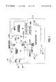
- FIG. 1is a schematic diagram showing an integrated circuit 10 having a function circuit 12 , a frequency synthesizer 20 and a testability circuit 50 .
- Embodiments in the present inventionfind particularly advantageous use when the integrated circuit 10 is an application specific integrated circuit (ASIC), which is an integrated circuit that has been built for a specific application.
- ASICapplication specific integrated circuit
- Integrated circuitsare traditionally designed with general purpose functions that allow designers to design systems in the form of integrated circuit boards by connecting integrated circuits with selected functions to one another.
- Designersmay use ASIC to consolidate many integrated circuits into a single package thereby reducing circuit board size requirements and power consumption.
- ASICSmay incorporate programmable logic arrays, field programmable gate arrays, cell based devices, and fully custom designed devices.
- the integrated circuit 10is preferably an ASIC that includes cell-based devices, or devices represented as cells.
- the cellsmay include design blocks for representing circuits in computer based design tools.
- Integrated circuit 10 in FIG. 1may be represented on a computer based design tool (described with reference to FIG. 4) using design blocks for the testability circuit 50 , the frequency synthesizer 20 , and the function circuit 12 .
- the testability circuit 50may also be included as a component of the frequency synthesizer 20 and represented as a single frequency synthesizer design block 15 .
- the single frequency synthesizer design block 15has the advantage of insuring that integrated circuit 10 will be testable because the testability function of the testability circuit 50 is built into the frequency synthesizer 15 .
- the testability functionis used any time the frequency synthesizer function is used.
- the function circuit 12includes circuitry required to perform any function desired by a designer of an integrated circuit 10 .
- the function circuit 12may include processing circuitry, memory, digital filters, combinational logic, counters, registers and any other integrated circuit or integrated circuit component needed to perform the function or functions desired by the designer. While FIG. 1 shows the function circuit 12 as one block, those of ordinary skill in the art will appreciate that many function blocks can be used, and thus, can be represented by the block representing the function circuit 12 .
- the function circuit 12includes pins or ports 32 for outputting signals to other circuitry to which it may be connected (not shown) or to pins and ports on the integrated circuit 10 .
- the function circuit 12includes a reset input for receiving a reset signal at connection 30 and a main clock input for receiving a clock signal at connection 40 .
- the function circuit 12also includes one or more frequency inputs, F 1 , F 2 , . . . F N .
- the frequency inputsreceive frequencies F 1,out , F 2,out , . . . , F N,out from the frequency synthesizer 20 at connections 22 ( 1 ), 22 ( 2 ), . . . 22 (N), respectively.
- the function circuit 12may be any circuit performing any function that makes advantageous use of a frequency synthesizer.
- the frequency synthesizer 20is preferably a complete frequency synthesizer phase-locked loop having multiple phased balanced output frequencies F 1 , F 2 , . . . F N .
- the frequency synthesizer 20may be used to generate a programmable clock source that is frequency and phase-locked to a highly referenced source such as a crystal oscillator.
- the crystal oscillatorpreferably resides external to the integrated circuit, although the location of the crystal oscillator is unimportant.
- the frequency synthesizer 20may be used with digital counters in order to obtain a complete frequency synthesis function.
- the countersmay be included in the cell; however, the frequency synthesizer 20 preferably does not include the counters since their implementation tends to be application-specific. In the integrated circuit 10 shown in FIG. 1, the counters used to complete the frequency synthesis function are included in the function circuit 12 .
- the frequency synthesizer 20includes a reference input for receiving a system clock signal at connection 14 .
- the frequency synthesizer 20uses a sequential logic phase/frequency detector for indicating when phase-lock has been attained.
- the phase/frequency detectordetects phase-lock by comparing the reference frequency with a feedback frequency, F 1,out .
- the feedback frequency F 1,outis input into a voltage controlled oscillator input, VCOIN on the frequency synthesizer 20 .
- the phase lockis indicated by outputting the lock signal at connection 28 .
- the testability circuit 50includes an input for receiving a master reset signal at connection 16 and a clock input for receiving the system clock signal at connection 14 .
- the testability circuit 50also includes a frequency synthesizer clock input for receiving the frequency F 1,out from the frequency synthesizer 20 at connection 24 .
- the frequency F 1,outis coupled to the voltage controlled oscillator input of the frequency synthesizer 20 at connection 26 .
- the voltage controlled oscillator input VCOIN of the frequency synthesizer 20is compared with the referenced frequency received at the referenced frequency input to determine when the phase lock loop has achieved the phase-lock state.
- the testability circuit 50uses select inputs SEL 0 and SEL 1 to set an operation mode for the integrated circuit 10 .
- the operation modemay include any number of test modes for testing any function and circuit in the integrated circuit 10 .
- the testability circuit 50includes a by-pass mode, a testability mode and a system mode.
- the by-pass modepermits the testing of the integrated circuit using automatic test equipment that may not be able to support the frequencies generated by the frequency synthesizer.
- the frequency outputs of the frequency synthesizer 20are not coupled to the function circuit 12 . Any necessary clock signals may be provided by an external oscillator or a frequency generated by the automatic test equipment.
- the output frequencies of the frequency synthesizer 20are coupled to the function circuit 12 .
- the integrated circuit 10is then provided with signals at its inputs and other control ports, or pins, that will generate desired test patterns at the outputs or other pins to the integrated circuit 10 .
- the clock signal from the frequency synthesizer 20is coupled to the function circuit 12 to provide an at-speed test.
- the at-speed testmay include a simulation of various circuits, components and functions in the integrated circuit 10 .
- Test patternsmay be generated by the at-speed test to determine the operability of the integrated circuit 10 during manufacturing. The test patterns are determined by the function of the integrated circuit 10 .
- the integrated circuitperforms the targeted system application for which the integrated circuit was designed.
- FIG. 2is a schematic diagram of an example of an implementation of the testability circuit 50 according to a preferred embodiment of the present invention.
- the testability circuit 50 in FIG. 2includes a first multiplexer 60 , a second multiplexer 70 , and a reset control circuit 80 .
- the first multiplexer 60receives a master clock signal from connection 14 at a first input 61 and a feedback frequency F 1,out from connection 22 ( 1 ), at a second input 63 .
- the first multiplexer 60receives a control signal at a control input 65 , from the first select input SEL 0 at connection 44 .
- the control signalis used to couple either the first input 61 or the second input to a first mux output 67 of the first multiplexer 60 .
- a ‘0’ state at the control input 65selects the first input 61 and a ‘1’ state selects the second input 63 .
- the second multiplexer 70is held to a logic state that simulates the phase-lock state of the frequency synthesizer 20 at a first input 71 and receives the lock signal from the frequency synthesizer 20 at connection 28 at a second input 73 .
- the second multiplexer 70receives a control signal at a control input 75 , from the first select input SEL 0 at connection 44 .
- the control signalis used to couple either the first input 71 or the second input 73 to the output 77 of the second multiplexer 70 .
- the signal that is output from the second mux output 77is a LOCK_IN signal which indicates a true phase-lock state when the second input 73 to the second multiplexer 70 is selected, or a simulated phase-lock state when the first input 71 is selected.
- the reset control circuit 80receives the LOCK_IN signal from the second multiplexer 70 , the second select input SEL 1 and the master reset signal from connection 16 .
- the reset control circuit 80outputs a reset signal at connection 30 to the function circuit 12 to trigger a reset when a phase lock is detected at the frequency synthesizer 20 . If the simulated phase-lock state is coupled to the reset circuit 80 through the LOCK_IN signal, the reset signal at connection 30 follows the master reset from connection 16 .
- testability circuit 50 in FIG. 2may conform to modes selected by the select inputs SEL 0 , SEL 1 .
- Table 1shows a truth table describing the by-pass, testability and system modes and the states of the select inputs necessary according to a preferred embodiment.
- the by-pass modeis selected whenever select input SEL 0 is logic ‘0’.
- SEL 0selects the lock signal received from the first input 61 and deselects the clock input received from the frequency synthesizer 20 at the second input 63 .
- the ‘0’ at the first select at SEL 0selects the first input 71 of the second multiplexer 70 which couples the lock signal at the LOCK_IN input of the reset control circuit 80 .
- the reset output at connection 30follows the master reset coming in from connection 16 .
- the testability modeis selected when the first select input SEL 0 is logic ‘1’ and the second select input SEL 1 is a ‘0’.
- the selection of a logic ‘1’ at the first select input SEL 0selects the F 1,out frequency from the frequency synthesizer 20 at the second input 63 . This causes the clock output at connection 40 to conduct a clock signal from the frequency synthesizer 20 .
- the logic ‘1’ at the first select input SEL 0also causes the second multiplexer 70 to couple the lock signal from the frequency synthesizer 20 at the second input 73 to the LOCK_IN input of the reset control circuit 80 .
- the testability modepermits the frequency synthesizer 20 to provide a clock signal at the clock output in connection 40 while the reset control circuit 80 insures that the reset output at connection 30 is not generated to the function circuit 12 until the lock state is detected in the frequency synthesizer 20 .
- FIG. 3shows an example of a reset control circuit 80 according to a preferred embodiment of the present invention.
- the reset control circuit 80includes a third multiplexer 94 a flip-flop 98 , a driver 90 an AND-gate 96 and a digital filter 92 .
- the first select input SEL 1triggers the third multiplexer 94 selecting either the first input 95 or the second input 97 .
- the first input 95is an output from the flip-flop 98 .
- the flip-flop 98receives the reset input from the driver 90 and uses the output of the AND-gate 96 to trigger the state of the reset input to the first input 95 of the third multiplexer 94 .
- the inputs to the AND-gate 96are the reset input and the lock signal from the output of the second multiplexer 70 in FIG. 2 .
- setting the second select input SEL 1 to logic ‘1’triggers the third multiplexer 94 to select the second input 97 which receives the reset signal from the master reset at connection 16 as shown in FIG. 2 .
- the reset control circuit 80By selecting the logic ‘1’ at the second selection input SEL 1 , the reset control circuit 80 causes the reset output to follow the master reset signal as is desired during normal operation of the system.
- the reset control circuit 80uses the output of the flip-flop 98 as the reset output. The output of the flip-flop 98 does not generate a reset signal unless the lock input indicates that the frequency synthesizer 20 is in phase lock, such that the integrated circuit is held in reset until the locked state is reached.
- the digital filter in 92is optional but advantageous to use to prevent false locks which may occur during the start up of the frequency synthesizer or by causing the integrated circuit 10 to come out of reset before it is desired.
- testability circuit 50 shown in FIG. 2 and the reset control circuit 80 shown in FIG. 3illustrate only one combination of gates, flip-flops, multiplexers and other combinational logic to insure the testability of the integrated circuit 10 during manufacturing and that other combinations are possible.
- truth table shown in Table 1illustrates only one example of the logic that may be used to insure the testability of the integrated circuit 10 during manufacturing.
- the logic ‘1’ and ‘0’ statesmay be implemented by any digital circuitry using a selected voltage for the one state and a selected alternative voltage for the logic ‘0’ state.
- the circuits shown in FIGS. 1, 2 and 3may be defined by cells in a computer based design tool.
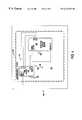
- FIG. 4shows a display 140 for a computer based designed tool in an integrated circuit design workstation.
- the display 140shows a function block 100 representing the integrated circuit 10 , a frequency synthesizer block 150 representing the frequency synthesizer 15 in FIG. 1 and a function circuit block 120 representing the function circuit 12 in FIG. 1.
- a designermay use the graphical user interface tools on the workstation to place the frequency synthesizer block 150 and the function circuit block 120 in any appropriate location on the integrated circuit design block 100 .
- the designermay use the graphical user interface to manipulate a pointer 125 using well-known graphical user interface tools to make connections between predefined output pins or input pins between the frequency synthesizer block 150 and the function circuit block 120 , as well as between the pins on the function blocks and the pins on the integrated circuit 100 .
- testability circuit 50may include in the frequency synthesizer block 150 to insure testability during manufacture of the integrated circuit 10 any time the frequency synthesizer block 150 is used.
Landscapes
- Engineering & Computer Science (AREA)
- General Engineering & Computer Science (AREA)
- Physics & Mathematics (AREA)
- General Physics & Mathematics (AREA)
- Semiconductor Integrated Circuits (AREA)
Abstract
Description
| TABLE 1 | ||||
| SEL0 | MODE | Description | ||
| 0 | 0 | Not Used | Not used, but same functionality as BYPASS | |
| mode. | ||||
| 0 | 1 | BYPASS | System clock bypasses | |
| 20. | ||||
| 1 | 0 | TEST- | ||
| ABILITY | used for at-speed tests. | |||
| 1 | 1 | SYSTEM | Testability logic bypassed for system | |
| application. | ||||
Claims (14)
Priority Applications (1)
| Application Number | Priority Date | Filing Date | Title |
|---|---|---|---|
| US09/212,769US6216254B1 (en) | 1998-12-16 | 1998-12-16 | Integrated circuit design using a frequency synthesizer that automatically ensures testability |
Applications Claiming Priority (1)
| Application Number | Priority Date | Filing Date | Title |
|---|---|---|---|
| US09/212,769US6216254B1 (en) | 1998-12-16 | 1998-12-16 | Integrated circuit design using a frequency synthesizer that automatically ensures testability |
Publications (1)
| Publication Number | Publication Date |
|---|---|
| US6216254B1true US6216254B1 (en) | 2001-04-10 |
Family
ID=22792360
Family Applications (1)
| Application Number | Title | Priority Date | Filing Date |
|---|---|---|---|
| US09/212,769Expired - LifetimeUS6216254B1 (en) | 1998-12-16 | 1998-12-16 | Integrated circuit design using a frequency synthesizer that automatically ensures testability |
Country Status (1)
| Country | Link |
|---|---|
| US (1) | US6216254B1 (en) |
Cited By (29)
| Publication number | Priority date | Publication date | Assignee | Title |
|---|---|---|---|---|
| US6510549B1 (en)* | 1999-02-17 | 2003-01-21 | Nec Corporation | Method of designing a semiconductor integrated circuit device in a short time |
| US20030200495A1 (en)* | 2002-04-17 | 2003-10-23 | Hitachi, Ltd. | Semiconductor integrated circuit and its design methodology |
| US6687866B2 (en)* | 1999-12-27 | 2004-02-03 | Nec Electronics Corporation | LSI having a built-in self-test circuit |
| US6847581B2 (en)* | 2002-01-11 | 2005-01-25 | Infineon Technologies Ag | Integrated circuit and method for operating the integrated circuit |
| US20060023544A1 (en)* | 2004-07-30 | 2006-02-02 | Fujitsu Limited | Semiconductor device |
| US7100139B1 (en)* | 2002-04-08 | 2006-08-29 | Cypress Semiconductor Corporation | Pinout views for allowed connections in GUI |
| US20080244480A1 (en)* | 2006-07-05 | 2008-10-02 | Chew Marko P | System and method to generate an IC layout using simplified manufacturing rule |
| US20080259998A1 (en)* | 2007-04-17 | 2008-10-23 | Cypress Semiconductor Corp. | Temperature sensor with digital bandgap |
| US20080297388A1 (en)* | 2007-04-17 | 2008-12-04 | Cypress Semiconductor Corporation | Programmable sigma-delta analog-to-digital converter |
| US20110029943A1 (en)* | 2009-07-30 | 2011-02-03 | Fujitsu Semiconductor Limited | Method for manufacturing semiconductor integrated circuit and recording medium |
| US8026739B2 (en) | 2007-04-17 | 2011-09-27 | Cypress Semiconductor Corporation | System level interconnect with programmable switching |
| US8049569B1 (en) | 2007-09-05 | 2011-11-01 | Cypress Semiconductor Corporation | Circuit and method for improving the accuracy of a crystal-less oscillator having dual-frequency modes |
| US8065653B1 (en) | 2007-04-25 | 2011-11-22 | Cypress Semiconductor Corporation | Configuration of programmable IC design elements |
| US8067948B2 (en) | 2006-03-27 | 2011-11-29 | Cypress Semiconductor Corporation | Input/output multiplexer bus |
| US8069405B1 (en) | 2001-11-19 | 2011-11-29 | Cypress Semiconductor Corporation | User interface for efficiently browsing an electronic document using data-driven tabs |
| US8078970B1 (en) | 2001-11-09 | 2011-12-13 | Cypress Semiconductor Corporation | Graphical user interface with user-selectable list-box |
| US8078894B1 (en) | 2007-04-25 | 2011-12-13 | Cypress Semiconductor Corporation | Power management architecture, method and configuration system |
| US8085067B1 (en) | 2005-12-21 | 2011-12-27 | Cypress Semiconductor Corporation | Differential-to-single ended signal converter circuit and method |
| US8085100B2 (en) | 2005-02-04 | 2011-12-27 | Cypress Semiconductor Corporation | Poly-phase frequency synthesis oscillator |
| US8103497B1 (en) | 2002-03-28 | 2012-01-24 | Cypress Semiconductor Corporation | External interface for event architecture |
| US8103496B1 (en) | 2000-10-26 | 2012-01-24 | Cypress Semicondutor Corporation | Breakpoint control in an in-circuit emulation system |
| US8120408B1 (en) | 2005-05-05 | 2012-02-21 | Cypress Semiconductor Corporation | Voltage controlled oscillator delay cell and method |
| US8130025B2 (en) | 2007-04-17 | 2012-03-06 | Cypress Semiconductor Corporation | Numerical band gap |
| US8160864B1 (en) | 2000-10-26 | 2012-04-17 | Cypress Semiconductor Corporation | In-circuit emulator and pod synchronized boot |
| US8358150B1 (en) | 2000-10-26 | 2013-01-22 | Cypress Semiconductor Corporation | Programmable microcontroller architecture(mixed analog/digital) |
| US8555032B2 (en) | 2000-10-26 | 2013-10-08 | Cypress Semiconductor Corporation | Microcontroller programmable system on a chip with programmable interconnect |
| US8793635B1 (en) | 2001-10-24 | 2014-07-29 | Cypress Semiconductor Corporation | Techniques for generating microcontroller configuration information |
| US9720805B1 (en) | 2007-04-25 | 2017-08-01 | Cypress Semiconductor Corporation | System and method for controlling a target device |
| US10698662B2 (en) | 2001-11-15 | 2020-06-30 | Cypress Semiconductor Corporation | System providing automatic source code generation for personalization and parameterization of user modules |
Citations (8)
| Publication number | Priority date | Publication date | Assignee | Title |
|---|---|---|---|---|
| US4477919A (en)* | 1981-04-06 | 1984-10-16 | Motorola, Inc. | Range control circuit for counter to be used in a frequency synthesizer |
| US4701920A (en)* | 1985-11-08 | 1987-10-20 | Eta Systems, Inc. | Built-in self-test system for VLSI circuit chips |
| US4795963A (en) | 1985-05-02 | 1989-01-03 | Hitachi, Ltd. | Test method of A/D converter |
| US5055800A (en) | 1990-04-30 | 1991-10-08 | Motorola, Inc. | Fractional n/m synthesis |
| US5125107A (en)* | 1989-03-02 | 1992-06-23 | Motorola, Inc. | Diagnostic mode for a frequency synthesizer |
| US5336939A (en) | 1992-05-08 | 1994-08-09 | Cyrix Corporation | Stable internal clock generation for an integrated circuit |
| US5422911A (en)* | 1993-09-17 | 1995-06-06 | Motorola, Inc. | Frequency walled phase lock loop |
| US5473651A (en) | 1994-12-28 | 1995-12-05 | At&T Corp. | Method and apparatus for testing large embedded counters |
- 1998
- 1998-12-16USUS09/212,769patent/US6216254B1/ennot_activeExpired - Lifetime
Patent Citations (8)
| Publication number | Priority date | Publication date | Assignee | Title |
|---|---|---|---|---|
| US4477919A (en)* | 1981-04-06 | 1984-10-16 | Motorola, Inc. | Range control circuit for counter to be used in a frequency synthesizer |
| US4795963A (en) | 1985-05-02 | 1989-01-03 | Hitachi, Ltd. | Test method of A/D converter |
| US4701920A (en)* | 1985-11-08 | 1987-10-20 | Eta Systems, Inc. | Built-in self-test system for VLSI circuit chips |
| US5125107A (en)* | 1989-03-02 | 1992-06-23 | Motorola, Inc. | Diagnostic mode for a frequency synthesizer |
| US5055800A (en) | 1990-04-30 | 1991-10-08 | Motorola, Inc. | Fractional n/m synthesis |
| US5336939A (en) | 1992-05-08 | 1994-08-09 | Cyrix Corporation | Stable internal clock generation for an integrated circuit |
| US5422911A (en)* | 1993-09-17 | 1995-06-06 | Motorola, Inc. | Frequency walled phase lock loop |
| US5473651A (en) | 1994-12-28 | 1995-12-05 | At&T Corp. | Method and apparatus for testing large embedded counters |
Cited By (45)
| Publication number | Priority date | Publication date | Assignee | Title |
|---|---|---|---|---|
| US6510549B1 (en)* | 1999-02-17 | 2003-01-21 | Nec Corporation | Method of designing a semiconductor integrated circuit device in a short time |
| US6687866B2 (en)* | 1999-12-27 | 2004-02-03 | Nec Electronics Corporation | LSI having a built-in self-test circuit |
| US8103496B1 (en) | 2000-10-26 | 2012-01-24 | Cypress Semicondutor Corporation | Breakpoint control in an in-circuit emulation system |
| US8555032B2 (en) | 2000-10-26 | 2013-10-08 | Cypress Semiconductor Corporation | Microcontroller programmable system on a chip with programmable interconnect |
| US9766650B2 (en) | 2000-10-26 | 2017-09-19 | Cypress Semiconductor Corporation | Microcontroller programmable system on a chip with programmable interconnect |
| US9843327B1 (en) | 2000-10-26 | 2017-12-12 | Cypress Semiconductor Corporation | PSOC architecture |
| US8358150B1 (en) | 2000-10-26 | 2013-01-22 | Cypress Semiconductor Corporation | Programmable microcontroller architecture(mixed analog/digital) |
| US10725954B2 (en) | 2000-10-26 | 2020-07-28 | Monterey Research, Llc | Microcontroller programmable system on a chip |
| US8160864B1 (en) | 2000-10-26 | 2012-04-17 | Cypress Semiconductor Corporation | In-circuit emulator and pod synchronized boot |
| US8736303B2 (en) | 2000-10-26 | 2014-05-27 | Cypress Semiconductor Corporation | PSOC architecture |
| US10261932B2 (en) | 2000-10-26 | 2019-04-16 | Cypress Semiconductor Corporation | Microcontroller programmable system on a chip |
| US10248604B2 (en) | 2000-10-26 | 2019-04-02 | Cypress Semiconductor Corporation | Microcontroller programmable system on a chip |
| US10020810B2 (en) | 2000-10-26 | 2018-07-10 | Cypress Semiconductor Corporation | PSoC architecture |
| US8793635B1 (en) | 2001-10-24 | 2014-07-29 | Cypress Semiconductor Corporation | Techniques for generating microcontroller configuration information |
| US10466980B2 (en) | 2001-10-24 | 2019-11-05 | Cypress Semiconductor Corporation | Techniques for generating microcontroller configuration information |
| US8078970B1 (en) | 2001-11-09 | 2011-12-13 | Cypress Semiconductor Corporation | Graphical user interface with user-selectable list-box |
| US10698662B2 (en) | 2001-11-15 | 2020-06-30 | Cypress Semiconductor Corporation | System providing automatic source code generation for personalization and parameterization of user modules |
| US8069405B1 (en) | 2001-11-19 | 2011-11-29 | Cypress Semiconductor Corporation | User interface for efficiently browsing an electronic document using data-driven tabs |
| US6847581B2 (en)* | 2002-01-11 | 2005-01-25 | Infineon Technologies Ag | Integrated circuit and method for operating the integrated circuit |
| US8103497B1 (en) | 2002-03-28 | 2012-01-24 | Cypress Semiconductor Corporation | External interface for event architecture |
| US7100139B1 (en)* | 2002-04-08 | 2006-08-29 | Cypress Semiconductor Corporation | Pinout views for allowed connections in GUI |
| US6907585B2 (en)* | 2002-04-17 | 2005-06-14 | Renesas Technology Corporation | Semiconductor integrated circuit and its design methodology |
| US20030200495A1 (en)* | 2002-04-17 | 2003-10-23 | Hitachi, Ltd. | Semiconductor integrated circuit and its design methodology |
| US20060023544A1 (en)* | 2004-07-30 | 2006-02-02 | Fujitsu Limited | Semiconductor device |
| US8085100B2 (en) | 2005-02-04 | 2011-12-27 | Cypress Semiconductor Corporation | Poly-phase frequency synthesis oscillator |
| US8120408B1 (en) | 2005-05-05 | 2012-02-21 | Cypress Semiconductor Corporation | Voltage controlled oscillator delay cell and method |
| US8085067B1 (en) | 2005-12-21 | 2011-12-27 | Cypress Semiconductor Corporation | Differential-to-single ended signal converter circuit and method |
| US8067948B2 (en) | 2006-03-27 | 2011-11-29 | Cypress Semiconductor Corporation | Input/output multiplexer bus |
| US8717042B1 (en) | 2006-03-27 | 2014-05-06 | Cypress Semiconductor Corporation | Input/output multiplexer bus |
| US7761824B2 (en)* | 2006-07-05 | 2010-07-20 | Chew Marko P | System and method to generate an IC layout using simplified manufacturing rule |
| US20080244480A1 (en)* | 2006-07-05 | 2008-10-02 | Chew Marko P | System and method to generate an IC layout using simplified manufacturing rule |
| US8092083B2 (en) | 2007-04-17 | 2012-01-10 | Cypress Semiconductor Corporation | Temperature sensor with digital bandgap |
| US8026739B2 (en) | 2007-04-17 | 2011-09-27 | Cypress Semiconductor Corporation | System level interconnect with programmable switching |
| US8476928B1 (en) | 2007-04-17 | 2013-07-02 | Cypress Semiconductor Corporation | System level interconnect with programmable switching |
| US20080259998A1 (en)* | 2007-04-17 | 2008-10-23 | Cypress Semiconductor Corp. | Temperature sensor with digital bandgap |
| US8130025B2 (en) | 2007-04-17 | 2012-03-06 | Cypress Semiconductor Corporation | Numerical band gap |
| US20080297388A1 (en)* | 2007-04-17 | 2008-12-04 | Cypress Semiconductor Corporation | Programmable sigma-delta analog-to-digital converter |
| US8040266B2 (en) | 2007-04-17 | 2011-10-18 | Cypress Semiconductor Corporation | Programmable sigma-delta analog-to-digital converter |
| US8065653B1 (en) | 2007-04-25 | 2011-11-22 | Cypress Semiconductor Corporation | Configuration of programmable IC design elements |
| US8078894B1 (en) | 2007-04-25 | 2011-12-13 | Cypress Semiconductor Corporation | Power management architecture, method and configuration system |
| US8499270B1 (en) | 2007-04-25 | 2013-07-30 | Cypress Semiconductor Corporation | Configuration of programmable IC design elements |
| US9720805B1 (en) | 2007-04-25 | 2017-08-01 | Cypress Semiconductor Corporation | System and method for controlling a target device |
| US8049569B1 (en) | 2007-09-05 | 2011-11-01 | Cypress Semiconductor Corporation | Circuit and method for improving the accuracy of a crystal-less oscillator having dual-frequency modes |
| US20110029943A1 (en)* | 2009-07-30 | 2011-02-03 | Fujitsu Semiconductor Limited | Method for manufacturing semiconductor integrated circuit and recording medium |
| US8281276B2 (en)* | 2009-07-30 | 2012-10-02 | Fujitsu Semiconductor Limited | Method for manufacturing semiconductor integrated circuit and recording medium |
Similar Documents
| Publication | Publication Date | Title |
|---|---|---|
| US6216254B1 (en) | Integrated circuit design using a frequency synthesizer that automatically ensures testability | |
| KR100506771B1 (en) | Event based semiconductor test system | |
| US20140101500A1 (en) | Circuits and methods for functional testing of integrated circuit chips | |
| US7571400B2 (en) | Chip design verifying and chip testing apparatus and method | |
| US5790563A (en) | Self test of core with unpredictable latency | |
| EP0330841B1 (en) | Logic circuit with a test function | |
| US6515549B2 (en) | Semiconductor device having critical path connected by feedback ring oscillator | |
| EP0530835A1 (en) | Testing circuit provided in digital logic circuits | |
| RU2260813C2 (en) | Check of the asynchronous reset of a circuit | |
| US6294935B1 (en) | Built-in-self-test circuitry for testing a phase locked loop circuit | |
| US20040085082A1 (en) | High -frequency scan testability with low-speed testers | |
| US6687890B2 (en) | Method for layout design and timing adjustment of logically designed integrated circuit | |
| US5799021A (en) | Method for direct access test of embedded cells and customization logic | |
| JPH0989980A (en) | Semiconductor integrated circuit and its evaluation method | |
| US6691289B2 (en) | Semiconductor integrated circuit including circuit for selecting embedded tap cores | |
| EP1233276B1 (en) | Boundary scan delay chain for crosschip delay measurement | |
| US7251761B2 (en) | Assembly for LSI test and method for the test | |
| US7146549B2 (en) | Scan-path flip-flop circuit for integrated circuit memory | |
| US20020199145A1 (en) | Semiconductor integrated circuits built therein scan paths | |
| US7194052B2 (en) | Data capture circuit with self-test capability | |
| WO2020038570A1 (en) | Extended jtag controller and method for functional reset using the extended jtag controller | |
| JPH05121666A (en) | Semiconductor integrated logic circuit | |
| US6691271B1 (en) | Built-in self-test apparatus | |
| CN114048702B (en) | Verification method for circuit comprising clock device and circuit | |
| EP3367114A1 (en) | Extended jtag controller and method for functional reset using the extended jtag controller |
Legal Events
| Date | Code | Title | Description |
|---|---|---|---|
| AS | Assignment | Owner name:LSI LOGIC CORPORATION, CALIFORNIA Free format text:ASSIGNMENT OF ASSIGNORS INTEREST;ASSIGNORS:PESCE, MICHAEL S.;GEARHARDT, KEVIN J.;KUPPINGER, JONATHAN P.;REEL/FRAME:009659/0397;SIGNING DATES FROM 19981214 TO 19981215 | |
| STCF | Information on status: patent grant | Free format text:PATENTED CASE | |
| FPAY | Fee payment | Year of fee payment:4 | |
| FEPP | Fee payment procedure | Free format text:PAYOR NUMBER ASSIGNED (ORIGINAL EVENT CODE: ASPN); ENTITY STATUS OF PATENT OWNER: LARGE ENTITY Free format text:PAYER NUMBER DE-ASSIGNED (ORIGINAL EVENT CODE: RMPN); ENTITY STATUS OF PATENT OWNER: LARGE ENTITY | |
| FPAY | Fee payment | Year of fee payment:8 | |
| FPAY | Fee payment | Year of fee payment:12 | |
| AS | Assignment | Owner name:DEUTSCHE BANK AG NEW YORK BRANCH, AS COLLATERAL AG Free format text:PATENT SECURITY AGREEMENT;ASSIGNORS:LSI CORPORATION;AGERE SYSTEMS LLC;REEL/FRAME:032856/0031 Effective date:20140506 | |
| AS | Assignment | Owner name:LSI CORPORATION, CALIFORNIA Free format text:CHANGE OF NAME;ASSIGNOR:LSI LOGIC CORPORATION;REEL/FRAME:033102/0270 Effective date:20070406 | |
| AS | Assignment | Owner name:AVAGO TECHNOLOGIES GENERAL IP (SINGAPORE) PTE. LTD Free format text:ASSIGNMENT OF ASSIGNORS INTEREST;ASSIGNOR:LSI CORPORATION;REEL/FRAME:035390/0388 Effective date:20140814 | |
| AS | Assignment | Owner name:AGERE SYSTEMS LLC, PENNSYLVANIA Free format text:TERMINATION AND RELEASE OF SECURITY INTEREST IN PATENT RIGHTS (RELEASES RF 032856-0031);ASSIGNOR:DEUTSCHE BANK AG NEW YORK BRANCH, AS COLLATERAL AGENT;REEL/FRAME:037684/0039 Effective date:20160201 Owner name:LSI CORPORATION, CALIFORNIA Free format text:TERMINATION AND RELEASE OF SECURITY INTEREST IN PATENT RIGHTS (RELEASES RF 032856-0031);ASSIGNOR:DEUTSCHE BANK AG NEW YORK BRANCH, AS COLLATERAL AGENT;REEL/FRAME:037684/0039 Effective date:20160201 | |
| AS | Assignment | Owner name:BANK OF AMERICA, N.A., AS COLLATERAL AGENT, NORTH CAROLINA Free format text:PATENT SECURITY AGREEMENT;ASSIGNOR:AVAGO TECHNOLOGIES GENERAL IP (SINGAPORE) PTE. LTD.;REEL/FRAME:037808/0001 Effective date:20160201 Owner name:BANK OF AMERICA, N.A., AS COLLATERAL AGENT, NORTH Free format text:PATENT SECURITY AGREEMENT;ASSIGNOR:AVAGO TECHNOLOGIES GENERAL IP (SINGAPORE) PTE. LTD.;REEL/FRAME:037808/0001 Effective date:20160201 | |
| AS | Assignment | Owner name:AVAGO TECHNOLOGIES GENERAL IP (SINGAPORE) PTE. LTD., SINGAPORE Free format text:TERMINATION AND RELEASE OF SECURITY INTEREST IN PATENTS;ASSIGNOR:BANK OF AMERICA, N.A., AS COLLATERAL AGENT;REEL/FRAME:041710/0001 Effective date:20170119 Owner name:AVAGO TECHNOLOGIES GENERAL IP (SINGAPORE) PTE. LTD Free format text:TERMINATION AND RELEASE OF SECURITY INTEREST IN PATENTS;ASSIGNOR:BANK OF AMERICA, N.A., AS COLLATERAL AGENT;REEL/FRAME:041710/0001 Effective date:20170119 | |
| AS | Assignment | Owner name:BELL SEMICONDUCTOR, LLC, ILLINOIS Free format text:ASSIGNMENT OF ASSIGNORS INTEREST;ASSIGNORS:AVAGO TECHNOLOGIES GENERAL IP (SINGAPORE) PTE. LTD.;BROADCOM CORPORATION;REEL/FRAME:044887/0109 Effective date:20171208 | |
| AS | Assignment | Owner name:CORTLAND CAPITAL MARKET SERVICES LLC, AS COLLATERA Free format text:SECURITY INTEREST;ASSIGNORS:HILCO PATENT ACQUISITION 56, LLC;BELL SEMICONDUCTOR, LLC;BELL NORTHERN RESEARCH, LLC;REEL/FRAME:045216/0020 Effective date:20180124 | |
| AS | Assignment | Owner name:BELL NORTHERN RESEARCH, LLC, ILLINOIS Free format text:RELEASE BY SECURED PARTY;ASSIGNOR:CORTLAND CAPITAL MARKET SERVICES LLC;REEL/FRAME:059720/0223 Effective date:20220401 Owner name:BELL SEMICONDUCTOR, LLC, ILLINOIS Free format text:RELEASE BY SECURED PARTY;ASSIGNOR:CORTLAND CAPITAL MARKET SERVICES LLC;REEL/FRAME:059720/0223 Effective date:20220401 Owner name:HILCO PATENT ACQUISITION 56, LLC, ILLINOIS Free format text:RELEASE BY SECURED PARTY;ASSIGNOR:CORTLAND CAPITAL MARKET SERVICES LLC;REEL/FRAME:059720/0223 Effective date:20220401 |