US6215686B1 - Memory system with switching for data isolation - Google Patents
Memory system with switching for data isolationDownload PDFInfo
- Publication number
- US6215686B1 US6215686B1US09/384,471US38447199AUS6215686B1US 6215686 B1US6215686 B1US 6215686B1US 38447199 AUS38447199 AUS 38447199AUS 6215686 B1US6215686 B1US 6215686B1
- Authority
- US
- United States
- Prior art keywords
- memory
- memory module
- pins
- couple
- signals
- Prior art date
- Legal status (The legal status is an assumption and is not a legal conclusion. Google has not performed a legal analysis and makes no representation as to the accuracy of the status listed.)
- Expired - Lifetime
Links
- 238000002955isolationMethods0.000titleclaims2
- 238000012546transferMethods0.000abstractdescription6
- 239000000872bufferSubstances0.000description46
- 238000010586diagramMethods0.000description14
- 238000004519manufacturing processMethods0.000description10
- 240000007320Pinus strobusSpecies0.000description7
- 239000003990capacitorSubstances0.000description7
- 230000003139buffering effectEffects0.000description5
- 230000006870functionEffects0.000description5
- 238000012360testing methodMethods0.000description5
- 230000005540biological transmissionEffects0.000description3
- 238000012986modificationMethods0.000description3
- 230000004048modificationEffects0.000description3
- 230000009977dual effectEffects0.000description2
- 230000005669field effectEffects0.000description2
- 238000013507mappingMethods0.000description2
- 230000005055memory storageEffects0.000description2
- 238000000034methodMethods0.000description2
- 230000004913activationEffects0.000description1
- 230000002457bidirectional effectEffects0.000description1
- 238000013481data captureMethods0.000description1
- 230000007547defectEffects0.000description1
- 230000000694effectsEffects0.000description1
- 238000007373indentationMethods0.000description1
- 238000009877renderingMethods0.000description1
- 230000000630rising effectEffects0.000description1
- 239000004065semiconductorSubstances0.000description1
- 230000008054signal transmissionEffects0.000description1
- 230000002459sustained effectEffects0.000description1
- 230000001360synchronised effectEffects0.000description1
Images


Classifications
- G—PHYSICS
- G11—INFORMATION STORAGE
- G11C—STATIC STORES
- G11C5/00—Details of stores covered by group G11C11/00
- G11C5/06—Arrangements for interconnecting storage elements electrically, e.g. by wiring
- G—PHYSICS
- G11—INFORMATION STORAGE
- G11C—STATIC STORES
- G11C5/00—Details of stores covered by group G11C11/00
- G11C5/02—Disposition of storage elements, e.g. in the form of a matrix array
- G11C5/04—Supports for storage elements, e.g. memory modules; Mounting or fixing of storage elements on such supports
- G—PHYSICS
- G11—INFORMATION STORAGE
- G11C—STATIC STORES
- G11C7/00—Arrangements for writing information into, or reading information out from, a digital store
- G11C7/10—Input/output [I/O] data interface arrangements, e.g. I/O data control circuits, I/O data buffers
- G11C7/1051—Data output circuits, e.g. read-out amplifiers, data output buffers, data output registers, data output level conversion circuits
- G11C7/1066—Output synchronization
- Y—GENERAL TAGGING OF NEW TECHNOLOGICAL DEVELOPMENTS; GENERAL TAGGING OF CROSS-SECTIONAL TECHNOLOGIES SPANNING OVER SEVERAL SECTIONS OF THE IPC; TECHNICAL SUBJECTS COVERED BY FORMER USPC CROSS-REFERENCE ART COLLECTIONS [XRACs] AND DIGESTS
- Y10—TECHNICAL SUBJECTS COVERED BY FORMER USPC
- Y10S—TECHNICAL SUBJECTS COVERED BY FORMER USPC CROSS-REFERENCE ART COLLECTIONS [XRACs] AND DIGESTS
- Y10S439/00—Electrical connectors
- Y10S439/955—Electrical connectors including electronic identifier or coding means
Definitions
- the present claimed inventionrelates to the field of memory storage systems. More particularly, the present invention relates to a memory storage system that includes a memory module on which memory devices are disposed.
- Recent computer systemsrequire faster microprocessors. These computer systems which require fast microprocessors require high memory bandwidth and high memory component capacity. This is particularly true in systems that contain multiple fast microprocessors.
- DIMMsDual Inline Memory Modules
- each DIMMincludes memory components that are Dynamic Random Access Memory (DRAM) semiconductor devices or Synchronous Dynamic Random Access Memory (SDRAM) devices.
- DRAMDynamic Random Access Memory
- SDRAMSynchronous Dynamic Random Access Memory
- Recent attempts to meet the demands of systems containing multiple fast microprocessorsinclude architectures that use data switching.
- Such systemsinclude Field Effect Transistors (FET) devices that operate as switches located on each memory module. These FET switches, in effect, switch off individual memory modules such that only one or two memory modules are transmitting data at any one time. This significantly reduces signal distortion.
- FETField Effect Transistors
- Memory modules that include FET switches located on each memory moduleare effective in reducing signal distortion.
- Such memory modulesare large and are expensive to manufacture.
- the inclusion of multiple FET switchesadds cost and increases the required size of each memory module.
- the connection schemeis complicated by the need to couple each data line to one or more FET. This results in a memory module that is complex and that is expensive to manufacture.
- Prior art memory modulestypically include terminal resistors located on each memory module. These terminal resistors couple to each data line. The terminal resistors take up valuable space on each memory module. Also, the terminal resistors increase the manufacturing cost of the memory module. In addition, such prior art memory modules typically include Series Stub Termination Logic (SSTL) which takes up valuable space on each memory module and increases the manufacturing cost of the memory module.
- SSTLSeries Stub Termination Logic
- a memory systemthat has a high memory component capacity and a high data bandwidth while minimizing distortion. Also, a memory system is needed that meets the above requirements and that includes a memory module that is inexpensive to manufacture. In addition, a memory system is needed that meets the above requirements and that includes a memory module that is smaller than prior art memory modules that include FET switches. The present invention provides an elegant solution to the above needs.
- the present inventionprovides a memory system and memory module that has a high memory component capacity and a high data bandwidth while minimizing distortion. This is achieved using a memory system that includes data switching but which does not include FET switches for data switching on each memory module. Also, individual memory modules do not include terminal resistors for data lines. This results in a memory module that is inexpensive to manufacture and that is smaller than prior art memory modules that include FET switches.
- a memory systemthat includes switches for controlling data transfer is disclosed.
- the memory systemincludes a memory controller that is coupled to a motherboard. Data switches are also disposed on the motherboard and are selectively coupled to the controller. Receptacles that are adapted to receive a memory module are coupled to the memory controller.
- the memory systemalso includes resistors that are coupled to Each connector receptacle for terminating data signals.
- the memory systemalso includes address/control buffers disposed on the motherboard that buffer address and control signals.
- address/control buffersdisposed on the motherboard that buffer address and control signals.
- the use of multiple address/control buffersprovides the necessary bandwidth so as to allow for fast access and control of memory components.
- memory modulesare accessed in pairs. That is, the data switches are used to control the flow of data signals such that data signals only flow to one pair of memory modules at any particular time. This allows for high-speed operation while minimizing distortion and interference between adjoining and nearby memory modules due to radio frequency interference.
- each memory moduleincludes twenty memory components. However, memory modules are adapted to be configured with fewer or more memory components on a given memory module. In one alternate embodiment, memory modules having forty memory components on each memory module are disclosed.
- the memory system of the present inventionincludes eight memory modules that use Double Data Rate (DDR) SDRAM memory components.
- the eight memory modulesare used in pairs.
- DDRDouble Data Rate
- this configurationgives a range of memory configurations from 128 megabytes (Mbytes) to 1 gigabyte (Gbyte).
- the memory system of the present inventionincludes resistors mounted on the motherboard and the same set of resistors is used to terminate data lines of multiple memory modules. Because only two memory modules are active at any time, only a sufficient number of resistors to terminate two memory modules is required. Thus, the memory system of the present invention requires fewer resistors than prior art memory systems that include memory modules that have resistors for data termination on each memory module (a full set of resistors is required on each prior art memory module). Because fewer resistors are required, the memory system of the present invention is less expensive than prior art memory systems that include memory modules that have resistors for data termination on each memory module.
- the memory system of the present inventionachieves a shorter circuit than that of prior art memory systems that include switches located on each memory module. That is, by placing the switches on the motherboard, there is no need to drive the connector receptacle and the circuitry on each memory module that leads to a switch as is required by prior art memory modules that include switches located on each memory module.
- switches placed on the motherboardsystem performance becomes more predictable. Any number of DIMMs (usually 1 to 4) can be placed in the memory system without affecting performance since the switches isolate unused DIMM connectors from the system. This allows for less performance variation, resulting in the ability to operate at the noted higher frequencies.
- the present inventionincludes switches placed on the motherboard. Thus, there is no need to place switches on each memory module. Because the memory modules of the present invention do not include switches, they are less expensive than prior art memory modules that include switches. Also, the memory modules of the present invention are less expensive because they do not require Series Stub Termination Logic (SSTL) related circuits on the memory module.
- SSTLSeries Stub Termination Logic
- the present inventionincludes resistors for data termination that are disposed on the motherboard. Thus, there is no need to place resistors on each memory module for terminating data lines. Because the memory module of the present invention does not include resistors, the memory module of the present invention is less expensive than prior art memory modules that include resistors for data line termination.
- the memory module of the present inventioncan be manufactured in a size that is physically smaller than the size of prior art memory modules. That is, because there is no need to place switches on each memory module, the memory module of the present invention can be made smaller than prior art memory modules that include switches. Also, because there is no need to place resistors on each memory module for terminating data lines, the memory module of the present invention can be made smaller than prior art memory modules that include resistors for data line termination.
- the memory system and memory module of the present inventionhas a high memory component capacity and a high data bandwidth while minimizing distortion. Also, the memory module of the present invention meets the above requirements and is inexpensive to manufacture. In addition, the memory module of the present invention is smaller than prior art memory modules that include switches.
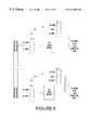
- FIG. 1is a diagram of a memory system showing a circuit board on which a connector receptacle and electronic circuitry is disposed and a memory module in accordance with the present claimed invention.
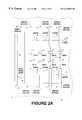
- FIG. 2Ais a top view showing a memory system that is adapted to receive eight memory modules in accordance with the present claimed invention.
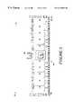
- FIG. 2Bis a diagram showing portions of a memory system that includes eight memory modules in accordance with the present claimed invention.
- FIG. 3is front side view of a memory module that includes twenty memory components in accordance with the present claimed invention.
- FIG. 4is rear side view of the memory module shown in FIG. 3 in accordance with the present claimed invention.
- FIG. 5is a diagram showing some of the components of a memory module that includes twenty memory components in accordance with the present claimed invention.
- FIG. 6is a diagram showing clock buffering and termination for a memory module that includes twenty memory components in accordance with the present claimed invention.
- FIG. 7is a diagram showing memory address and control buffering for a memory module that includes twenty memory components in accordance with the present claimed invention.
- FIG. 8is diagram showing connections to clock buffers and resistors that couple to the clock buffers for a memory module that includes twenty memory components in accordance with the present claimed invention.
- FIG. 9is diagram showing connections to address/control buffers and capacitors and resistors that couple to the address/control buffers for a memory module that includes twenty memory components in accordance with the present claimed invention.
- FIG. 10is a diagram showing an identification device for a memory module that includes twenty memory components in accordance with the present claimed invention.
- FIG. 11is a diagram showing connections to the memory components of bank A for a memory module that includes twenty memory components in accordance with the present claimed invention.
- FIG. 12is a diagram showing connections to the memory components of bank B for a memory module that includes twenty memory components in accordance with the present claimed invention.
- FIG. 13is a diagram showing connections to memory components that are used to store directory data for a memory module that includes twenty memory components in accordance with the present claimed invention.
- FIG. 14is a diagram showing reference Voltage (V REF ) generation and bypassing for a memory module that includes twenty memory components in accordance with the present claimed invention.
- FIG. 15is a diagram showing Voltage bypassing for a memory module that includes twenty memory components in accordance with the present claimed invention.
- FIG. 16is a diagram showing pin connections for a memory module that includes twenty memory components in accordance with the present claimed invention.
- FIG. 17is a chart showing pin connections and functions for a memory module that includes twenty memory components in accordance with the present claimed invention.
- FIG. 18is a chart showing pin connections and functions and descriptions for a memory module that includes twenty memory components in accordance with the present claimed invention.
- FIG. 19is a chart showing timing conditions for a memory module that includes twenty memory components in accordance with the present claimed invention.
- FIG. 20is a front view of a memory module that includes forty memory components in accordance with one embodiment of the present claimed invention.
- FIG. 21is a rear view of a memory module of FIG. 20 in accordance with one embodiment of the present claimed invention.
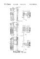
- memory system 10is shown to include electrical circuitry 11 that is disposed on circuit board 16 .
- Connector receptacle 12is also disposed on circuit board 16 and is electrically coupled to electrical circuitry 11 .
- Memory module 4includes circuit card 2 and memory components 3 . Memory components 3 are attached to circuit board 2 and are electrically connected to contact pads 6 via conductive traces (not shown).
- memory module 4is a Dual Inline Memory Module (DIMM) and memory components 3 are Dynamic Random-Access Memory (DRAM) devices.
- the DRAM devices that are usedare DDR SDRAM devices that use an internal, pipelined double-data-rate architecture to achieve high-speed operation.
- memory module 4includes identification device 1 that allows for identification of memory module 4 .
- identification device 1stores a serial number and/or other data that identifies memory module 4 .
- electrical circuitry 11includes electrical circuits that allow for the operation of only those memory modules that include authorized identification data. This prevents use of unauthorized memory modules. Thus, reducing down time and defects related to the use of sub-standard memory modules.
- memory module 4is inserted into connector receptacle 12 .
- Individual contact pads of contact pads 6also referred to as “pins” make electrical contact with corresponding sockets (not shown) in connector receptacle 12 so as to electrically connect the electrical circuits on memory module 4 to the electrical circuitry 11 located on circuit board 16 .
- Clips 15hold memory module 4 securely in place when it is inserted into connector receptacle 12 .
- Alignment notches within connector receptacle 12engage indentations 7 - 9 on memory module 4 so as to provides for proper alignment and positioning of memory module 4 .
- FIG. 2Ashows a memory system 100 that includes a circuit board 16 on which connector receptacles 21 - 28 are disposed.
- Connector receptacles 21 - 28are adapted to receive up to 8 memory modules (not shown).
- connector receptacles 21 - 28are adapted to receive memory modules that include 294-pin RIMM style edge connectors.
- Memory system 100includes memory controller 20 that is electrically connected to connector receptacles 21 - 28 by data bus 30 and address/control bus 32 .
- Resistors, shown generally as resistors 41 - 48electrically couple to connector receptacles 21 - 28 for terminating data lines.
- resistors 41 - 44couple to connector receptacles 21 - 24 for termination of data lines coupled to connector receptacles 21 - 24 .
- resistors 45 - 48couple to connector receptacles 25 - 28 for termination of data lines coupled to connector receptacles 25 - 28 .
- memory controller 20includes logic for detecting the identification of memory modules. That is, memory module 20 determines whether any memory module inserted into ones of connector receptacles 21 - 28 includes an identification device (e.g. identification device 1 of FIG. 1) that includes information identifying the memory module as being an authorized memory module. If the memory module is an authorized memory module, the memory module will be used to store and retrieve data. However, if the memory module is not identified as an authorized memory module, memory controller 20 generates an error message and will not use the memory module for storing and retrieving data. This prevents the use of sub-standard memory modules and memory components.
- an identification devicee.g. identification device 1 of FIG. 1
- address/control buffersshown generally as address/control buffers 35 are disposed between memory controller 20 and connector receptacles 21 - 28 .
- address/control buffers 35includes seven buffers that are coupled to address/control bus 32 such that they are electrically coupled to memory controller 20 and to connector receptacles 21 - 28 .
- data bus 30includes 216 data lines that couple to connector receptacles 21 - 28 , with 108 data lines selectively coupled to each of connector receptacles 21 , 23 , 25 and 27 , and with 108 data lines selectively coupled to each of connector receptacles 22 , 24 , 26 , and 28 .
- the memory modules (not shown) disposed in connector receptacles connector receptacles 21 , 23 , 25 and 27operate as a first bank of memory modules and the memory modules disposed in connector receptacles 22 , 24 , 26 , and 28 operate as a second bank of memory modules.
- switches 51 - 58are coupled to data bus 30 so as to selectively allow data to be coupled to connector receptacles 21 - 28 . More particularly, switches 51 - 58 couple to data lines of data bus 32 so as to selectively allow data to flow to only to those memory modules that are active at a particular time when memory modules are disposed in connector receptacles 21 - 28 . In one embodiment, switches 51 - 58 are Field Effect Transistors (FETs) that operate so as to selectively activate pairs of memory modules such that only two memory modules are active at any one time when memory modules are disposed in connector receptacles 21 - 28 .
- FETsField Effect Transistors
- each of switches 51 - 58consists of 6 individual 20-bit switches. This gives a total of 48 20-bit switches. By preventing unnecessary data transmission, switches 51 - 58 decrease signal distortion and interference resulting from radio frequency transmission.
- switches 51 - 58operate to selectively allow data to pass to ones of connector receptacles 21 - 29 such that only two memory modules are active at any time.
- switches 52 - 54 and switches 56 - 58are selectively closed while switches 51 and 55 are open for driving the memory modules in connector receptacles 21 - 22 .
- switches 51 , 53 - 55 and 57 - 58are selectively closed while switches 52 and 56 are open for driving the memory modules in connector receptacles 23 - 24 .
- Memory modules disposed in connector receptacles 25 - 26are driven by opening switches 53 and 57 and closing switches 51 - 52 , 54 - 56 and 58 .
- Memory modules disposed in connector receptacles 27 - 28are driven by opening switches 54 and 58 and closing switches 51 - 53 and 55 - 57 .
- FIG. 2Bshows an embodiment of a memory system 200 that includes memory modules that are DIMMs (shown as DIMM 0 -DIMM 7 ).
- DIMM 0 -DIMM 7are disposed in each of connector receptacles 21 - 28 of FIG. 2 a.
- address/control buffers 35 of FIG. 2Ainclude seven buffers, shown as buffers 101 - 107 .
- buffer 101is a (SSTL) buffer that couples address signals to DIMM 0 -DIMM 3
- buffer 102is a SSTL buffer that couples address signals to DIMM 4 -DIMM 7 .
- Buffers 103 - 106selectively couple control signals to DIMM 0 -DIMM 7 .
- memory system 100 of FIG. 2Ais shown to include eight connector receptacles, in an alternate embodiment, fewer or more connector receptacles could be used.
- memory system 200 of FIG. 2Bcould include more or fewer DIMMs.
- FIGS. 3-19show a specific embodiment of a memory module 300 that includes twenty memory components.
- memory module 300includes two banks of memory components.
- Bank A of memory componentsis disposed on the front side of memory module 300 and bank B is disposed on the rear side of memory module 300 .
- Bank Aincludes memory components A 0 -A 9 .
- Memory components A 0 -A 9are attached to circuit card 301 and are selectively electrically coupled to contact pads 303 by conductive traces (not shown).
- contact pads 303are comprised of 294 individual contact pads, referred to hereinafter as pins 1 - 294 .
- memory components A 0 -A 9are selectively electrically coupled to ones of pins 1 - 294 .
- bank Bincludes memory components B 0 -B 9 .
- Memory components B 0 -B 9are attached to circuit card 301 and are selectively electrically coupled to pins 1 - 294 by conductive traces (not shown).
- memory components A 0 -A 9 of FIG. 3 and memory components B 0 -B 9 of FIG. 4are 8 megabit by 8 DDR SDRAMs configured to store 72 bits of data for a data density of 128 Megabytes.
- memory components A 0 -A 9 of FIG. 3 and memory components B 0 -B 9 of FIG. 4are 16 megabit by 8 DDR SDRAMs configured to store 72 bits of data for a data density of 256 Megabytes.
- Contact pads 303 of FIGS. 3-4includes a total of 294 pins, with pins 1 - 147 located on the front side of memory module 300 (FIG. 3) and pins 148 - 294 disposed on the rear side of memory module 300 (FIG. 4 ).
- the present inventionis well adapted for using a greater or lesser number of pins.
- clock buffer 304is disposed on the front side of memory module 300 and clock buffer 305 is disposed on the rear side of memory module 300 .
- clock buffers 304 - 305are 1:10 clock buffers.
- address/control buffer 306is disposed on the front side of memory module 300 and address/control buffer 307 is disposed on the rear side of memory module 300 .
- address/control buffers 306 - 307are 20-bit buffers that operate at 3.5 nanoseconds (ns).
- identification device 308provides for identification of memory module 300 .
- Identification device 308is attached to circuit board 301 and is selectively electrically coupled to ones of pins 1 - 294 by conductive lines (not shown).
- identification device 308is a serial Electrical Erasable Programmable Read Only Memory (EEPROM) device that stores data pertaining to memory module 300 .
- EEPROMElectrical Erasable Programmable Read Only Memory
- identification device 308stores a serial number, the type of memory components A 0 -A 9 and B 0 -B 9 , the manufacturer, the date of manufacture, and the amount of memory on the memory module.
- FIG. 5shows memory components A 0 -A 8 to be coupled to data lines for the storage of data.
- memory module 300includes 72 main memory data input and output signals and 16 directory memory data input and output signals.
- Memory component A 9is used for storing a directory. That is, directory information is stored in memory component A 9 that indicates the location of data in memory components A 0 -A 8 .
- memory components B 0 -B 8(not shown) are also coupled to data lines for the storage of data.
- Memory component B 9(not shown) is used for storing a directory that indicates the location of data in memory components B 0 -B 8 .
- main memory(A 0 -A 8 and B 0 -B 8 ) and directory memory (A 9 and B 9 ) have separate control and addressing with a common clock.
- the differential clock inputis buffered on the memory module 300 by clock buffers 304 - 305 .
- Address and control signalsare buffered on the memory module by buffers 306 - 307 .
- Identification device 308is selectively coupled to pins 1 - 294 for identification of memory module 300 .
- resistorsshown generally as resistors 310 are coupled to clock buffer 304 .
- Clock buffer 304is electrically coupled to ones of pins 1 - 294 and to DRAMS A 0 -A 9 .
- resistors 310are coupled to clock buffer 305 .
- Clock buffer 305is electrically coupled to ones of pins 1 - 294 and to DRAMS B 0 -B 9 .
- FIG. 7shows address/control buffers 306 - 307 to be selectively electrically connected to pins 1 - 294 and to ones of memory components A 0 -A 8 and B 0 -B 8 . More particularly, address/control buffer 306 is electrically coupled to resistors, shown generally as resistors 310 , and to memory components A 0 -A 8 . Address/control buffer 307 is electrically coupled to resistors 310 and to memory components B 0 -B 8 .
- Clock buffer 306is shown to be electrically coupled to memory components A 0 -A 2 , B 0 -B 2 , A 7 -A 9 , and to B 7 -B 9 .
- Clock buffer 307is electrically coupled to memory components A 3 -A 6 and B 3 -B 6 .
- Clock buffers 306 - 307are also electrically coupled to resistors, shown generally as resistors 310 .
- FIG. 9shows data address/control buffer connections and terminations.
- Address/control buffer 306couples to memory components A 0 -A 8 and to resistors, shown generally as resistors 310 .
- address/control buffer 307couples to memory components B 0 -B 8 and to resistors 310 .
- Address/control buffer 307is selectively coupled to ones of resistors 310 by capacitors, shown generally as capacitors 311 .
- identification device 308is coupled to capacitors, shown generally as capacitors 311 .
- identification device 308is a 256 ⁇ 8 bit, 2-wire, serial EEPROM.
- identification device 308stores a serial number and information indicating the type of memory components used (e.g. manufacturer, date of manufacture, part number, etc.).
- connections to memory components A 0 -A 8are shown.
- Datais addressed through 14 address lines, shown as DATA ADDR 0 A-DATA ADDR 13 A, that couple to each of memory components A 0 -A 8 .
- Datais coupled from memory components A 0 -A 8 over a total of 72 data lines, shown as data lines MB DATA 0 -MB DATA 71 .
- FIG. 12shows connections to memory components B 0 -B 8 .
- Datais addressed through 14 address lines, shown as DATA ADDR 0 B-DATA ADDR 13 B, that couple to each of memory components B 0 -B 8 .
- Datais coupled from memory components B 0 -B 8 over a total of 72 data lines, shown as data lines MB DATA 0 -MB DATA 71 .
- FIG. 13shows connections to memory components A 9 and B 9 .
- memory components A 0 and B 9operate as a directory for memory components A 0 -A 8 and B 0 -B 8 .
- Memory component A 9couples to 16 lines of directory data, shown as DB DATA 0 -DB DATA 15 for output of directory data.
- Memory component A 9is addressed through 14 directory address lines, shown as DB ADDR 0 -DB ADDR 13 .
- DB ADDR 0 -DB ADDR 1316 lines of directory data, shown as DB DATA 0 -DB DATA 15 for output of directory data.
- Memory component B 9is addressed through 14 directory address lines, shown as DB ADDR 0 -DB ADDR 13 .
- Reference voltage generation and bypassing circuitsare shown in FIGS. 14 and 15 to include resistors, shown generally as resistor 310 , and capacitors, shown generally as capacitors 311 .
- FIG. 16shows connections to individual pins of contact pads 303 .
- Each of the 294 individual pins of contact pads 303is assigned a number from 1 to 294.
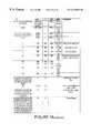
- FIG. 17shows the functions assigned to each particular pin of pins 1 - 294 .
- FIG. 18include a chart showing pins, signals, input and output (I/O, signal type, name and definitions for various signals.
- pins 70 and 71couple clock signals (CK).
- Pin 215couples clock enable (CKE) signals.
- Pins 217 - 218couple chip select signals (CS). Row address strobe (RAS) signals are conveyed through pin 65 . Column address strobe (CAS) signals are conveyed through pin 214 . Write enable (WE) signals are conveyed through pin 67 .
- Main memory address signals (A 0 -A 12 )are coupled through pins 55 , 56 , 58 , 59 , 61 , 62 , 202 , 203 , 205 , 206 , 208 , 209 , 211 .
- Bank address (BA 0 , BA 1 ) signalscoupled through pins 64 and 211 , defining to which bank an activate, read, write, or precharge command is being applied.
- data input and output signalsare conveyed through pins 5 , 7 , 11 , 13 , 15 , 17 , 21 , 23 , 25 , 27 , 31 , 33 , 35 , 37 , 41 , 43 , 45 , 47 , 51 , 53 , 75 , 77 , 81 , 83 , 85 , 87 , 91 , 93 , 95 , 97 , 101 , 103 , 105 , 107 , 109 , 111 , 113 , 152 , 154 , 158 , 160 , 162 , 164 , 168 , 170 , 172 , 174 , 178 , 180 , 182 , 184 , 188 , 190 , 192 , 194 , 198 , 200 , 222 , 224 , 228 , 230 , 232 , 234 , 238 ,
- Directory related signalsinclude signals for chip select (pins 293 , 146 ), row address strobe (pin 143 ), column address strobe (pin 292 ), write enable (pin 145 ), directory address (pins 133 - 134 , 136 - 137 , 139 - 140 , 280 - 281 , 283 - 284 , 286 - 287 ), directory bank address (pins 142 - 290 ), directory data I/O (pins 115 , 117 , 119 , 121 , 125 , 127 , 129 , 131 , 262 , 263 , 266 , 268 , 272 , 274 , 276 , 278 ) and directory data strobe (pins 123 , 270 ).
- Testing related signalsinclude signals for test port clock (pin 1 ), test data in (pin 2 ), test data out (pin 3 ), test mode select (pin 149 ). Other signals include signals for serial data line (pin 73 ), serial data clock pin 220 ) and write protect ( 68 ).
- V DDPower supply
- V DDPower supply
- Output data Power supply(V DDO ) is provided (2.5 Volt) through pins 6 , 14 , 22 , 30 , 38 , 46 , 54 , 76 , 84 , 92 , 100 , 116 , 124 , 132 , 153 , 161 , 169 , 177 , 185 , 193 , 201 , 223 , 231 , 239 , 247 , 255 , 263 , 271 and 279 .
- GNDElectrical ground
- timing conditionsmeet the criteria specified in FIG. 19 as indicated in nanoseconds (ns) clock cycles (t CK ) milliseconds (ms), or picoseconds (ps).
- Data access time, Data output hold time, Data output low impedance, and Data output high impedanceare measured from the clock signal's rising edge.
- Row cycle timeis measured from refresh/activate to refresh/activate.
- Row access timeis from row address to read data, and Row precharge time is from precharge to refresh/activate.
- memory devicesare Double Data Rate SDRAMs that use a 2n prefetch architecture to achieve high-speed operation by interface designed to transfer two data words per clock cycle at the I/O pins of the SDRAM.
- a single read or write access for the each DDR SDRAMconsists of a single, one clock cycle data transfer at the internal SDRAM core and two corresponding one-half-clock cycle data transfer at the data I/O pins of the SDRAM.
- the bidirectional data strobes (DQS(n))are transferred externally, along with data, for use in data capture at the receiver.
- DQSis an intermittent strobe transmitted by memory components during READs and by the memory controller during WRITEs.
- DQSis edge-aligned with data for READs and center-aligned with data for WRITEs.
- the memory componentsoperate from a differential clock. Commands (address and control signals) are registered at every positive edge of CK. Input data is registered on both edges of DQS, and output data is referenced to both edges of DQS, as well as to both edges of CK. Read and write accesses to the memory components are burst oriented; accesses start at a selected location and continue for a programmed number of locations in a programmed sequence.
- Accessbegins with the registration of an ACTIVATE command, which is then followed by a READ or Write command.
- the address bits registered coincident with the Activate commandare used to select the bank and row to be accessed (BA 0 -BA 1 select the bank; A 0 -A 11 select the row).
- the address bits registered coincident with the READ or WRITE commandare used to select the starting column location for the burst access.
- the memory componentprovides for programmable READ or WRITE burst lengths of 2, 4, or 8 locations.
- An AUTO PRECHARGE functionmay be enabled to provide a self-timed row precharge that is initiated at the end of the burst sequence.
- the pipelined, multiband architecture of the present inventionallows for concurrent operation, thereby providing high effective bandwidth by hiding row precharge and activation time.
- An auto refresh modeis provided, along with a power-saving, power-down mode.
- all inputsare compatible with the JDEC Standard for SSTL 2 and all outputs are SSTL 2, Class II compatible.
- the memory components of the present inventionmay be addressed such that different parts of a memory word may be separately addressed with a unique address. This allows for the access of unaligned data in a single memory clock period. This is particularly advantageous for 3D graphics applications such as texture mapping where data structures may not be ideally aligned with respect to the memory word. This allows for accessing unaligned texture mapping data in a sustained fashion by presenting different address information on one or more of the address busses every memory clock period.
- the system memory module of the present inventionmeets the needs of recent graphics rendering engines and provides good 3D Graphics performance.
- burst lengthis programmable such that read and write access to memory components can be controlled.
- the burst lengthdetermines the maximum number of column locations that can be accessed for a given READ or WRITE command. Burst lengths of 2, 4, or 8 locations are available for both the sequential and the interleaved burst types.
- a READ or WRITE commandis issued, a block of columns equal to the burst length is effectively selected. All access for that burst take place within this block, meaning that the burst will wrap within the block if a boundary is reached.
- the blockis uniquely selected by A 1 -A 8 when the burst length is set to two.
- the blockis uniquely selected by A 3 -A 8 when the burst length is set to four and by A 3 -A 8 when the burst length is set to eight.
- the remaining (least significant) address bitsare used to select the starting location within the block.
- the programmed burst lengthapplies to both READ and WRITE bursts.
- FIGS. 20-21show an embodiment that includes a memory module 400 that includes 40 memory components.
- memory components 401 - 420are disposed on the front side of memory module 400 .
- memory modules 401 - 409 and 411 - 419form a main memory bank while memory modules 410 and 420 are used for directory data.
- memory components 421 - 440are disposed on the rear side of memory module 400 .
- memory modules 421 - 429 and 431 - 439form a main memory bank while memory modules 430 and 440 are used for directory data.
- Memory module 400 of FIGS. 20-21also includes clock buffers 451 - 452 and address/control buffers 453 - 454 for clock buffering and buffering of address and control signals.
- Identification device 450allows for identification of memory module 400 .
- the memory system of the present inventionincludes resistors mounted on the motherboard and the same set of resistors is used to terminate data lines of multiple memory modules. Because only two memory modules are active at any time, only a sufficient number of resistors to terminate two memory modules is required. Thus, the memory system of the present invention requires fewer resistors than prior art memory systems that include memory modules that have resistors for data termination on each memory module (a full set of resistors is required on each prior art memory module). Because fewer resistors are required, the memory system of the present invention is less expensive than prior art memory systems that include memory modules that have resistors for data termination on each memory module.
- the memory system of the present inventionachieves a shorter circuit than that of prior art memory systems that include switches located on each memory module. That is, by placing the switches on the motherboard, there is no need to drive the connector receptacle and the circuitry on each memory module that leads to a switch as is required by prior art memory modules that include switches located on each memory module. This also results in reduced distortion and interference resulting from radio frequency interference.
- the present inventionincludes switches placed on the motherboard. Thus, there is no need to place switches on each memory module. Because the memory modules of the present invention do not include switches, they are less expensive than prior art memory modules that include switches. Also, the memory modules of the present invention are less expensive because they do not require Series Stub Termination Logic (SSTL) related circuits on the memory module.
- SSTLSeries Stub Termination Logic
- the present inventionincludes resistors for data termination that are disposed on the motherboard. Thus, there is no need to place resistors on each memory module for terminating data lines. Because the memory module of the present invention does not include resistors, the memory module of the present invention is less expensive than prior art memory modules that include resistors for data line termination.
- the memory module of the present inventioncan be manufactured in a size that is physically smaller than the size of prior art memory modules. That is, because there is no need to place switches on each memory module, the memory module of the present invention can be made smaller than prior art memory modules that include switches. Also, because there is no need to place resistors on each memory module for terminating data lines, the memory module of the present invention can be made smaller than prior art memory modules that include resistors for data line termination.
- the memory system and memory module of the present inventionhas a high memory component capacity and a high data bandwidth while minimizing distortion. Also, the memory module of the present invention meets the above requirements and is inexpensive to manufacture. In addition, the memory module of the present invention is smaller than prior art memory modules that include switches.
Landscapes
- Dram (AREA)
Abstract
Description
Claims (19)
Priority Applications (1)
| Application Number | Priority Date | Filing Date | Title |
|---|---|---|---|
| US09/384,471US6215686B1 (en) | 1999-02-09 | 1999-08-27 | Memory system with switching for data isolation |
Applications Claiming Priority (2)
| Application Number | Priority Date | Filing Date | Title |
|---|---|---|---|
| US09/247,256US6115278A (en) | 1999-02-09 | 1999-02-09 | Memory system with switching for data isolation |
| US09/384,471US6215686B1 (en) | 1999-02-09 | 1999-08-27 | Memory system with switching for data isolation |
Related Parent Applications (1)
| Application Number | Title | Priority Date | Filing Date |
|---|---|---|---|
| US09/247,256DivisionUS6115278A (en) | 1999-02-09 | 1999-02-09 | Memory system with switching for data isolation |
Publications (1)
| Publication Number | Publication Date |
|---|---|
| US6215686B1true US6215686B1 (en) | 2001-04-10 |
Family
ID=22934237
Family Applications (2)
| Application Number | Title | Priority Date | Filing Date |
|---|---|---|---|
| US09/247,256Expired - LifetimeUS6115278A (en) | 1999-02-09 | 1999-02-09 | Memory system with switching for data isolation |
| US09/384,471Expired - LifetimeUS6215686B1 (en) | 1999-02-09 | 1999-08-27 | Memory system with switching for data isolation |
Family Applications Before (1)
| Application Number | Title | Priority Date | Filing Date |
|---|---|---|---|
| US09/247,256Expired - LifetimeUS6115278A (en) | 1999-02-09 | 1999-02-09 | Memory system with switching for data isolation |
Country Status (1)
| Country | Link |
|---|---|
| US (2) | US6115278A (en) |
Cited By (45)
| Publication number | Priority date | Publication date | Assignee | Title |
|---|---|---|---|---|
| US20020004893A1 (en)* | 2000-01-25 | 2002-01-10 | Nai-Shung Chang | Feedback system for accomodating different memory module loading |
| US6466472B1 (en)* | 2001-04-13 | 2002-10-15 | Giga-Byte Technology Co., Ltd. | Common module for DDR SDRAM and SDRAM |
| DE10120418A1 (en)* | 2001-04-26 | 2002-11-07 | Giga Byte Technology Co | Common module for DDR SDRAM and SDRAM, has terminators connected to common module to output termination voltage and controller to transmit common/address and data signals to common module |
| US20030206164A1 (en)* | 2002-05-01 | 2003-11-06 | Juenger Randall E. | Dynamic switching of parallel termination for power management with DDR memory |
| US6665736B1 (en)* | 2000-04-13 | 2003-12-16 | Acer Laboratories, Inc. | Computer motherboard for supporting various memories |
| US6741497B2 (en)* | 2001-08-30 | 2004-05-25 | Micron Technology, Inc. | Flash memory with RDRAM interface |
| US6771553B2 (en) | 2001-10-18 | 2004-08-03 | Micron Technology, Inc. | Low power auto-refresh circuit and method for dynamic random access memories |
| US20040184324A1 (en)* | 2002-06-07 | 2004-09-23 | Pax George E | Reduced power registered memory module and method |
| US20050094425A1 (en)* | 2003-10-30 | 2005-05-05 | Mike Cogdill | Double-high memory ststem compatible with termination schemes for single-high memory systems |
| US20060023482A1 (en)* | 2004-07-30 | 2006-02-02 | International Business Machines Corporation | 276-Pin buffered memory module with enhanced fault tolerance |
| US20060026349A1 (en)* | 2004-07-30 | 2006-02-02 | International Business Machines Corporaiton | System, method and storage medium for providing a serialized memory interface with a bus repeater |
| US20060036826A1 (en)* | 2004-07-30 | 2006-02-16 | International Business Machines Corporation | System, method and storage medium for providing a bus speed multiplier |
| US20060095701A1 (en)* | 2004-10-29 | 2006-05-04 | International Business Machines Corporation | System, method and storage medium for a memory subsystem with positional read data latency |
| US20060095646A1 (en)* | 2004-10-29 | 2006-05-04 | International Business Machines Corporation | System, method and storage medium for a memory subsystem command interface |
| US20060095629A1 (en)* | 2004-10-29 | 2006-05-04 | International Business Machines Corporation | System, method and storage medium for providing a service interface to a memory system |
| US20060107186A1 (en)* | 2004-10-29 | 2006-05-18 | International Business Machines Corporation | System, method and storage medium for providing a high speed test interface to a memory subsystem |
| US20060117233A1 (en)* | 2004-10-29 | 2006-06-01 | International Business Machines Corporation | System, Method and storage medium for testing a memory module |
| US20070101086A1 (en)* | 2005-10-31 | 2007-05-03 | International Business Machines Corporation | System, method and storage medium for deriving clocks in a memory system |
| US20070160053A1 (en)* | 2005-11-28 | 2007-07-12 | Coteus Paul W | Method and system for providing indeterminate read data latency in a memory system |
| US20070218741A1 (en)* | 2006-03-16 | 2007-09-20 | Lenovo Pte. Ltd. | Apparatus and method for component module insertion and removal protection |
| US7277988B2 (en) | 2004-10-29 | 2007-10-02 | International Business Machines Corporation | System, method and storage medium for providing data caching and data compression in a memory subsystem |
| US20070276977A1 (en)* | 2006-05-24 | 2007-11-29 | International Business Machines Corporation | Systems and methods for providing memory modules with multiple hub devices |
| US20070276976A1 (en)* | 2006-05-24 | 2007-11-29 | International Business Machines Corporation | Systems and methods for providing distributed technology independent memory controllers |
| US7305574B2 (en) | 2004-10-29 | 2007-12-04 | International Business Machines Corporation | System, method and storage medium for bus calibration in a memory subsystem |
| US20070288707A1 (en)* | 2006-06-08 | 2007-12-13 | International Business Machines Corporation | Systems and methods for providing data modification operations in memory subsystems |
| US20070300129A1 (en)* | 2004-10-29 | 2007-12-27 | International Business Machines Corporation | System, method and storage medium for providing fault detection and correction in a memory subsystem |
| US20080005479A1 (en)* | 2006-05-22 | 2008-01-03 | International Business Machines Corporation | Systems and methods for providing remote pre-fetch buffers |
| US20080034148A1 (en)* | 2006-08-01 | 2008-02-07 | International Business Machines Corporation | Systems and methods for providing performance monitoring in a memory system |
| US20080040562A1 (en)* | 2006-08-09 | 2008-02-14 | International Business Machines Corporation | Systems and methods for providing distributed autonomous power management in a memory system |
| US20080040563A1 (en)* | 2006-08-10 | 2008-02-14 | International Business Machines Corporation | Systems and methods for memory module power management |
| US20080094811A1 (en)* | 2006-10-23 | 2008-04-24 | International Business Machines Corporation | High density high reliability memory module with a fault tolerant address and command bus |
| US20080115137A1 (en)* | 2006-08-02 | 2008-05-15 | International Business Machines Corporation | Systems and methods for providing collision detection in a memory system |
| US20080133797A1 (en)* | 2004-07-30 | 2008-06-05 | International Business Machines Corporation | System, method and storage medium for a multi-mode memory buffer device |
| US20080162991A1 (en)* | 2007-01-02 | 2008-07-03 | International Business Machines Corporation | Systems and methods for improving serviceability of a memory system |
| US20080183903A1 (en)* | 2007-01-29 | 2008-07-31 | International Business Machines Corporation | Systems and methods for providing dynamic memory pre-fetch |
| US7490217B2 (en) | 2006-08-15 | 2009-02-10 | International Business Machines Corporation | Design structure for selecting memory busses according to physical memory organization information stored in virtual address translation tables |
| US20090119114A1 (en)* | 2007-11-02 | 2009-05-07 | David Alaniz | Systems and Methods for Enabling Customer Service |
| US7539842B2 (en) | 2006-08-15 | 2009-05-26 | International Business Machines Corporation | Computer memory system for selecting memory buses according to physical memory organization information stored in virtual address translation tables |
| US7539800B2 (en) | 2004-07-30 | 2009-05-26 | International Business Machines Corporation | System, method and storage medium for providing segment level sparing |
| US7606988B2 (en) | 2007-01-29 | 2009-10-20 | International Business Machines Corporation | Systems and methods for providing a dynamic memory bank page policy |
| US20090300260A1 (en)* | 2008-05-28 | 2009-12-03 | Rambus Inc. | Selective switching of a memory bus |
| US20100191880A1 (en)* | 2004-03-08 | 2010-07-29 | Samsung Electronics Co., Ltd. | Memory module capable of improving the integrity of signals transmitted through a data bus and a command/address bus, and a memory system including the same |
| US20100269012A1 (en)* | 2006-10-23 | 2010-10-21 | International Business Machines Corporation | High Density High Reliability Memory Module with Power Gating and a Fault Tolerant Address and Command Bus |
| US7868652B1 (en) | 2009-12-08 | 2011-01-11 | International Business Machines Corporation | Off-die termination module with a spring loaded pin in a DIMM socket |
| US7868651B1 (en) | 2009-12-08 | 2011-01-11 | International Business Machines Corporation | Off-die termination of memory module signal lines |
Families Citing this family (34)
| Publication number | Priority date | Publication date | Assignee | Title |
|---|---|---|---|---|
| US6914905B1 (en) | 2000-06-16 | 2005-07-05 | Extreme Networks, Inc. | Method and system for VLAN aggregation |
| US6510100B2 (en) | 2000-12-04 | 2003-01-21 | International Business Machines Corporation | Synchronous memory modules and memory systems with selectable clock termination |
| US6912592B2 (en)* | 2001-01-05 | 2005-06-28 | Extreme Networks, Inc. | Method and system of aggregate multiple VLANs in a metropolitan area network |
| US6721185B2 (en)* | 2001-05-01 | 2004-04-13 | Sun Microsystems, Inc. | Memory module having balanced data I/O contacts pads |
| DE10122701A1 (en)* | 2001-05-10 | 2002-11-21 | Infineon Technologies Ag | circuit module |
| US6711027B2 (en)* | 2001-07-23 | 2004-03-23 | Intel Corporation | Modules having paths of different impedances |
| US6918078B2 (en)* | 2001-07-23 | 2005-07-12 | Intel Corporation | Systems with modules sharing terminations |
| US6771515B2 (en)* | 2001-07-23 | 2004-08-03 | Intel Corporation | Systems having modules with on die terminations |
| US6674648B2 (en)* | 2001-07-23 | 2004-01-06 | Intel Corporation | Termination cards and systems therefore |
| US6724082B2 (en) | 2001-07-23 | 2004-04-20 | Intel Corporation | Systems having modules with selectable on die terminations |
| US6631083B2 (en) | 2001-07-23 | 2003-10-07 | Intel Corporation | Systems with modules and clocking therefore |
| US6674649B2 (en)* | 2001-07-23 | 2004-01-06 | Intel Corporation | Systems having modules sharing on module terminations |
| US6538951B1 (en)* | 2001-08-30 | 2003-03-25 | Micron Technology, Inc. | Dram active termination control |
| KR100429878B1 (en)* | 2001-09-10 | 2004-05-03 | 삼성전자주식회사 | Memory module and printed circuit board for the same |
| US8837161B2 (en)* | 2002-07-16 | 2014-09-16 | Nvidia Corporation | Multi-configuration processor-memory substrate device |
| JP4233360B2 (en)* | 2003-03-07 | 2009-03-04 | 三菱電機株式会社 | Printed circuit board for high-speed communication |
| US7149841B2 (en)* | 2003-03-31 | 2006-12-12 | Micron Technology, Inc. | Memory devices with buffered command address bus |
| TW585384U (en)* | 2003-06-12 | 2004-04-21 | Via Tech Inc | Motherboard |
| US20060118950A1 (en)* | 2003-07-03 | 2006-06-08 | Smart Modular Technologies, Inc., A California Corporation | Multi function module |
| US8250295B2 (en) | 2004-01-05 | 2012-08-21 | Smart Modular Technologies, Inc. | Multi-rank memory module that emulates a memory module having a different number of ranks |
| US7289386B2 (en) | 2004-03-05 | 2007-10-30 | Netlist, Inc. | Memory module decoder |
| US7916574B1 (en) | 2004-03-05 | 2011-03-29 | Netlist, Inc. | Circuit providing load isolation and memory domain translation for memory module |
| US8040710B2 (en)* | 2007-05-31 | 2011-10-18 | Qimonda Ag | Semiconductor memory arrangement |
| TWI352357B (en)* | 2007-06-05 | 2011-11-11 | Asustek Comp Inc | Motherboard and memory device thereof |
| US8516185B2 (en) | 2009-07-16 | 2013-08-20 | Netlist, Inc. | System and method utilizing distributed byte-wise buffers on a memory module |
| US8154901B1 (en) | 2008-04-14 | 2012-04-10 | Netlist, Inc. | Circuit providing load isolation and noise reduction |
| US8417870B2 (en) | 2009-07-16 | 2013-04-09 | Netlist, Inc. | System and method of increasing addressable memory space on a memory board |
| US9128632B2 (en) | 2009-07-16 | 2015-09-08 | Netlist, Inc. | Memory module with distributed data buffers and method of operation |
| JP2011029535A (en) | 2009-07-29 | 2011-02-10 | Elpida Memory Inc | Semiconductor device |
| CN103809708A (en) | 2012-11-07 | 2014-05-21 | 辉达公司 | Panel electronic device, auxiliary heat dissipating device of panel electronic device and assembly of panel electronic device and auxiliary heat dissipating device |
| US10324841B2 (en) | 2013-07-27 | 2019-06-18 | Netlist, Inc. | Memory module with local synchronization |
| EP3058571A1 (en)* | 2013-10-15 | 2016-08-24 | Rambus Inc. | Load reduced memory module |
| US9954557B2 (en)* | 2014-04-30 | 2018-04-24 | Microsoft Technology Licensing, Llc | Variable width error correction |
| US20220358072A1 (en)* | 2022-07-26 | 2022-11-10 | Intel Corporation | Memory module adapter card with multiplexer circuitry |
Citations (15)
| Publication number | Priority date | Publication date | Assignee | Title |
|---|---|---|---|---|
| US5283877A (en) | 1990-07-17 | 1994-02-01 | Sun Microsystems, Inc. | Single in-line DRAM memory module including a memory controller and cross bar switches |
| US5319591A (en) | 1991-12-26 | 1994-06-07 | Oki Electric Industry Co., Ltd. | Memory module |
| US5341331A (en) | 1991-07-31 | 1994-08-23 | Samsung Electronics, Co., Ltd. | Data transmission circuit having common input/output lines |
| US5357624A (en) | 1991-10-23 | 1994-10-18 | Ast Research, Inc. | Single inline memory module support system |
| US5383148A (en) | 1992-05-19 | 1995-01-17 | Sun Microsystems, Inc. | Single in-line memory module |
| US5513135A (en) | 1994-12-02 | 1996-04-30 | International Business Machines Corporation | Synchronous memory packaged in single/dual in-line memory module and method of fabrication |
| US5564107A (en) | 1991-11-13 | 1996-10-08 | Atalla; Martin M. | Microcell computer system and method using cell access switch and moving memory architecture |
| US5646904A (en) | 1994-10-25 | 1997-07-08 | Oki Electric Industry Co., Ltd. | Semicoductor memory with a timing controlled for receiving data at a semiconductor memory module to be accessed |
| US5661677A (en) | 1996-05-15 | 1997-08-26 | Micron Electronics, Inc. | Circuit and method for on-board programming of PRD Serial EEPROMS |
| US5691950A (en) | 1996-01-19 | 1997-11-25 | Sgs-Thomson Microelectronics, Inc. | Device and method for isolating bit lines from a data line |
| US5761132A (en) | 1995-10-17 | 1998-06-02 | Samsung Electronic Co., Ltd. | Integrated circuit memory devices with latch-free page buffers therein for preventing read failures |
| US5802395A (en) | 1996-07-08 | 1998-09-01 | International Business Machines Corporation | High density memory modules with improved data bus performance |
| US5870325A (en)* | 1998-04-14 | 1999-02-09 | Silicon Graphics, Inc. | Memory system with multiple addressing and control busses |
| US5926838A (en) | 1997-03-19 | 1999-07-20 | Micron Electronics | Interface for high speed memory |
| US5945886A (en) | 1996-09-20 | 1999-08-31 | Sldram, Inc. | High-speed bus structure for printed circuit boards |
Family Cites Families (5)
| Publication number | Priority date | Publication date | Assignee | Title |
|---|---|---|---|---|
| US5272664A (en)* | 1993-04-21 | 1993-12-21 | Silicon Graphics, Inc. | High memory capacity DRAM SIMM |
| US5530623A (en)* | 1993-11-19 | 1996-06-25 | Ncr Corporation | High speed memory packaging scheme |
| US5578940A (en)* | 1995-04-04 | 1996-11-26 | Rambus, Inc. | Modular bus with single or double parallel termination |
| IN188196B (en)* | 1995-05-15 | 2002-08-31 | Silicon Graphics Inc | |
| US5953215A (en)* | 1997-12-01 | 1999-09-14 | Karabatsos; Chris | Apparatus and method for improving computer memory speed and capacity |
- 1999
- 1999-02-09USUS09/247,256patent/US6115278A/ennot_activeExpired - Lifetime
- 1999-08-27USUS09/384,471patent/US6215686B1/ennot_activeExpired - Lifetime
Patent Citations (15)
| Publication number | Priority date | Publication date | Assignee | Title |
|---|---|---|---|---|
| US5283877A (en) | 1990-07-17 | 1994-02-01 | Sun Microsystems, Inc. | Single in-line DRAM memory module including a memory controller and cross bar switches |
| US5341331A (en) | 1991-07-31 | 1994-08-23 | Samsung Electronics, Co., Ltd. | Data transmission circuit having common input/output lines |
| US5357624A (en) | 1991-10-23 | 1994-10-18 | Ast Research, Inc. | Single inline memory module support system |
| US5564107A (en) | 1991-11-13 | 1996-10-08 | Atalla; Martin M. | Microcell computer system and method using cell access switch and moving memory architecture |
| US5319591A (en) | 1991-12-26 | 1994-06-07 | Oki Electric Industry Co., Ltd. | Memory module |
| US5383148A (en) | 1992-05-19 | 1995-01-17 | Sun Microsystems, Inc. | Single in-line memory module |
| US5646904A (en) | 1994-10-25 | 1997-07-08 | Oki Electric Industry Co., Ltd. | Semicoductor memory with a timing controlled for receiving data at a semiconductor memory module to be accessed |
| US5513135A (en) | 1994-12-02 | 1996-04-30 | International Business Machines Corporation | Synchronous memory packaged in single/dual in-line memory module and method of fabrication |
| US5761132A (en) | 1995-10-17 | 1998-06-02 | Samsung Electronic Co., Ltd. | Integrated circuit memory devices with latch-free page buffers therein for preventing read failures |
| US5691950A (en) | 1996-01-19 | 1997-11-25 | Sgs-Thomson Microelectronics, Inc. | Device and method for isolating bit lines from a data line |
| US5661677A (en) | 1996-05-15 | 1997-08-26 | Micron Electronics, Inc. | Circuit and method for on-board programming of PRD Serial EEPROMS |
| US5802395A (en) | 1996-07-08 | 1998-09-01 | International Business Machines Corporation | High density memory modules with improved data bus performance |
| US5945886A (en) | 1996-09-20 | 1999-08-31 | Sldram, Inc. | High-speed bus structure for printed circuit boards |
| US5926838A (en) | 1997-03-19 | 1999-07-20 | Micron Electronics | Interface for high speed memory |
| US5870325A (en)* | 1998-04-14 | 1999-02-09 | Silicon Graphics, Inc. | Memory system with multiple addressing and control busses |
Cited By (122)
| Publication number | Priority date | Publication date | Assignee | Title |
|---|---|---|---|---|
| US20020004893A1 (en)* | 2000-01-25 | 2002-01-10 | Nai-Shung Chang | Feedback system for accomodating different memory module loading |
| US6745275B2 (en)* | 2000-01-25 | 2004-06-01 | Via Technologies, Inc. | Feedback system for accomodating different memory module loading |
| US6665736B1 (en)* | 2000-04-13 | 2003-12-16 | Acer Laboratories, Inc. | Computer motherboard for supporting various memories |
| US6466472B1 (en)* | 2001-04-13 | 2002-10-15 | Giga-Byte Technology Co., Ltd. | Common module for DDR SDRAM and SDRAM |
| DE10120418B4 (en)* | 2001-04-26 | 2008-04-30 | Giga-Byte Technology Co., Ltd., Hsin-Tien | Common module for DDR SDRAM and SDRAM |
| DE10120418A1 (en)* | 2001-04-26 | 2002-11-07 | Giga Byte Technology Co | Common module for DDR SDRAM and SDRAM, has terminators connected to common module to output termination voltage and controller to transmit common/address and data signals to common module |
| US6741497B2 (en)* | 2001-08-30 | 2004-05-25 | Micron Technology, Inc. | Flash memory with RDRAM interface |
| US6901008B2 (en) | 2001-08-30 | 2005-05-31 | Micron Technology, Inc. | Flash memory with RDRAM interface |
| US20040165432A1 (en)* | 2001-08-30 | 2004-08-26 | Micron Technology, Inc. | Flash memory with RDRAM interface |
| US20040165433A1 (en)* | 2001-08-30 | 2004-08-26 | Micron Technology, Inc. | Flash memory with RDRAM interface |
| US20040168015A1 (en)* | 2001-08-30 | 2004-08-26 | Micron Technology, Inc. | Flash memory with RDRAM interface |
| US6980453B2 (en) | 2001-08-30 | 2005-12-27 | Micron Technology, Inc. | Flash memory with RDRAM interface |
| US6906955B2 (en) | 2001-08-30 | 2005-06-14 | Micron Technology, Inc. | Flash memory with RDRAM interface |
| US20040268018A1 (en)* | 2001-10-18 | 2004-12-30 | Cowles Timothy B | Low power auto-refresh circuit and method for dynamic random access memories |
| US6771553B2 (en) | 2001-10-18 | 2004-08-03 | Micron Technology, Inc. | Low power auto-refresh circuit and method for dynamic random access memories |
| US7079439B2 (en) | 2001-10-18 | 2006-07-18 | Micron Technology, Inc. | Low power auto-refresh circuit and method for dynamic random access memories |
| US6894691B2 (en)* | 2002-05-01 | 2005-05-17 | Dell Products L.P. | Dynamic switching of parallel termination for power management with DDR memory |
| US20030206164A1 (en)* | 2002-05-01 | 2003-11-06 | Juenger Randall E. | Dynamic switching of parallel termination for power management with DDR memory |
| US20040184324A1 (en)* | 2002-06-07 | 2004-09-23 | Pax George E | Reduced power registered memory module and method |
| US20060028904A1 (en)* | 2002-06-07 | 2006-02-09 | Micron Technology, Inc. | Reduced power registered memory module and method |
| US7180797B2 (en) | 2002-06-07 | 2007-02-20 | Micron Technology, Inc. | Reduced power registered memory module and method |
| US7072231B2 (en) | 2002-06-07 | 2006-07-04 | Micron Technology, Inc. | Reduced power registered memory module and method |
| US20050094425A1 (en)* | 2003-10-30 | 2005-05-05 | Mike Cogdill | Double-high memory ststem compatible with termination schemes for single-high memory systems |
| US7054179B2 (en)* | 2003-10-30 | 2006-05-30 | Hewlett-Packard Development Company, L.P. | Double-high memory system compatible with termination schemes for single-high memory systems |
| US8117363B2 (en)* | 2004-03-08 | 2012-02-14 | Samsung Electronics Co., Ltd. | Memory module capable of improving the integrity of signals transmitted through a data bus and a command/address bus, and a memory system including the same |
| US20100191880A1 (en)* | 2004-03-08 | 2010-07-29 | Samsung Electronics Co., Ltd. | Memory module capable of improving the integrity of signals transmitted through a data bus and a command/address bus, and a memory system including the same |
| US20080133797A1 (en)* | 2004-07-30 | 2008-06-05 | International Business Machines Corporation | System, method and storage medium for a multi-mode memory buffer device |
| US20070288679A1 (en)* | 2004-07-30 | 2007-12-13 | International Business Machines Corporation | 276-pin buffered memory module with enhanced fault tolerance and a performance-optimized pin assignment |
| US7765368B2 (en) | 2004-07-30 | 2010-07-27 | International Business Machines Corporation | System, method and storage medium for providing a serialized memory interface with a bus repeater |
| US7551468B2 (en)* | 2004-07-30 | 2009-06-23 | International Business Machines Corporation | 276-pin buffered memory module with enhanced fault tolerance |
| US7539810B2 (en) | 2004-07-30 | 2009-05-26 | International Business Machines Corporation | System, method and storage medium for a multi-mode memory buffer device |
| US7539800B2 (en) | 2004-07-30 | 2009-05-26 | International Business Machines Corporation | System, method and storage medium for providing segment level sparing |
| US7224595B2 (en)* | 2004-07-30 | 2007-05-29 | International Business Machines Corporation | 276-Pin buffered memory module with enhanced fault tolerance |
| US20060026349A1 (en)* | 2004-07-30 | 2006-02-02 | International Business Machines Corporaiton | System, method and storage medium for providing a serialized memory interface with a bus repeater |
| US7529112B2 (en)* | 2004-07-30 | 2009-05-05 | International Business Machines Corporation | 276-Pin buffered memory module with enhanced fault tolerance and a performance-optimized pin assignment |
| US20060023482A1 (en)* | 2004-07-30 | 2006-02-02 | International Business Machines Corporation | 276-Pin buffered memory module with enhanced fault tolerance |
| US20080183957A1 (en)* | 2004-07-30 | 2008-07-31 | International Business Machines Corporation | 276-pin buffered memory module with enhanced fault tolerance |
| US20070255902A1 (en)* | 2004-07-30 | 2007-11-01 | International Business Machines Corporation | System, method and storage medium for providing a serialized memory interface with a bus repeater |
| US7296129B2 (en) | 2004-07-30 | 2007-11-13 | International Business Machines Corporation | System, method and storage medium for providing a serialized memory interface with a bus repeater |
| US7389375B2 (en) | 2004-07-30 | 2008-06-17 | International Business Machines Corporation | System, method and storage medium for a multi-mode memory buffer device |
| US20060036826A1 (en)* | 2004-07-30 | 2006-02-16 | International Business Machines Corporation | System, method and storage medium for providing a bus speed multiplier |
| US7484161B2 (en) | 2004-10-29 | 2009-01-27 | International Business Machines Corporation | System, method and storage medium for providing fault detection and correction in a memory subsystem |
| US7441060B2 (en) | 2004-10-29 | 2008-10-21 | International Business Machines Corporation | System, method and storage medium for providing a service interface to a memory system |
| US7590882B2 (en) | 2004-10-29 | 2009-09-15 | International Business Machines Corporation | System, method and storage medium for bus calibration in a memory subsystem |
| US20060107186A1 (en)* | 2004-10-29 | 2006-05-18 | International Business Machines Corporation | System, method and storage medium for providing a high speed test interface to a memory subsystem |
| US20060095629A1 (en)* | 2004-10-29 | 2006-05-04 | International Business Machines Corporation | System, method and storage medium for providing a service interface to a memory system |
| US20070294466A1 (en)* | 2004-10-29 | 2007-12-20 | International Business Machines Corporation | System, method and storage medium for a memory subsystem command interface |
| US20070300129A1 (en)* | 2004-10-29 | 2007-12-27 | International Business Machines Corporation | System, method and storage medium for providing fault detection and correction in a memory subsystem |
| US20090150636A1 (en)* | 2004-10-29 | 2009-06-11 | International Business Machines Corporation | Memory subsystem with positional read data latency |
| US20080016281A1 (en)* | 2004-10-29 | 2008-01-17 | International Business Machines Corporation | System, method and storage medium for providing data caching and data compression in a memory subsystem |
| US20060117233A1 (en)* | 2004-10-29 | 2006-06-01 | International Business Machines Corporation | System, Method and storage medium for testing a memory module |
| US8589769B2 (en) | 2004-10-29 | 2013-11-19 | International Business Machines Corporation | System, method and storage medium for providing fault detection and correction in a memory subsystem |
| US20060095646A1 (en)* | 2004-10-29 | 2006-05-04 | International Business Machines Corporation | System, method and storage medium for a memory subsystem command interface |
| US20080040569A1 (en)* | 2004-10-29 | 2008-02-14 | International Business Machines Corporation | System, method and storage medium for bus calibration in a memory subsystem |
| US20080046796A1 (en)* | 2004-10-29 | 2008-02-21 | International Business Machines Corporation | System, method and storage medium for providing fault detection and correction in a memory subsystem |
| US20080046795A1 (en)* | 2004-10-29 | 2008-02-21 | International Business Machines Corporation | System, method and storage medium for providing fault detection and correction in a memory subsystem |
| US7844771B2 (en) | 2004-10-29 | 2010-11-30 | International Business Machines Corporation | System, method and storage medium for a memory subsystem command interface |
| US7356737B2 (en) | 2004-10-29 | 2008-04-08 | International Business Machines Corporation | System, method and storage medium for testing a memory module |
| US7512762B2 (en) | 2004-10-29 | 2009-03-31 | International Business Machines Corporation | System, method and storage medium for a memory subsystem with positional read data latency |
| US20060095701A1 (en)* | 2004-10-29 | 2006-05-04 | International Business Machines Corporation | System, method and storage medium for a memory subsystem with positional read data latency |
| US8296541B2 (en) | 2004-10-29 | 2012-10-23 | International Business Machines Corporation | Memory subsystem with positional read data latency |
| US7610423B2 (en) | 2004-10-29 | 2009-10-27 | International Business Machines Corporation | Service interface to a memory system |
| US7299313B2 (en) | 2004-10-29 | 2007-11-20 | International Business Machines Corporation | System, method and storage medium for a memory subsystem command interface |
| US7392337B2 (en) | 2004-10-29 | 2008-06-24 | International Business Machines Corporation | System, method and storage medium for a memory subsystem command interface |
| US7395476B2 (en) | 2004-10-29 | 2008-07-01 | International Business Machines Corporation | System, method and storage medium for providing a high speed test interface to a memory subsystem |
| US7480759B2 (en) | 2004-10-29 | 2009-01-20 | International Business Machines Corporation | System, method and storage medium for providing data caching and data compression in a memory subsystem |
| US20080177929A1 (en)* | 2004-10-29 | 2008-07-24 | International Business Machines Corporation | System, method and storage medium for a memory subsystem command interface |
| US7277988B2 (en) | 2004-10-29 | 2007-10-02 | International Business Machines Corporation | System, method and storage medium for providing data caching and data compression in a memory subsystem |
| US7480830B2 (en) | 2004-10-29 | 2009-01-20 | International Business Machines Corporation | System, method and storage medium for testing a memory module |
| US7305574B2 (en) | 2004-10-29 | 2007-12-04 | International Business Machines Corporation | System, method and storage medium for bus calibration in a memory subsystem |
| US7451273B2 (en) | 2004-10-29 | 2008-11-11 | International Business Machines Corporation | System, method and storage medium for providing data caching and data compression in a memory subsystem |
| US20080313374A1 (en)* | 2004-10-29 | 2008-12-18 | International Business Machines Corporation | Service interface to a memory system |
| US7475316B2 (en) | 2004-10-29 | 2009-01-06 | International Business Machines Corporation | System, method and storage medium for providing a high speed test interface to a memory subsystem |
| US8140942B2 (en) | 2004-10-29 | 2012-03-20 | International Business Machines Corporation | System, method and storage medium for providing fault detection and correction in a memory subsystem |
| US7934115B2 (en) | 2005-10-31 | 2011-04-26 | International Business Machines Corporation | Deriving clocks in a memory system |
| US20070101086A1 (en)* | 2005-10-31 | 2007-05-03 | International Business Machines Corporation | System, method and storage medium for deriving clocks in a memory system |
| US7478259B2 (en) | 2005-10-31 | 2009-01-13 | International Business Machines Corporation | System, method and storage medium for deriving clocks in a memory system |
| US20090094476A1 (en)* | 2005-10-31 | 2009-04-09 | International Business Machines Corporation | Deriving clocks in a memory system |
| US20070160053A1 (en)* | 2005-11-28 | 2007-07-12 | Coteus Paul W | Method and system for providing indeterminate read data latency in a memory system |
| US8495328B2 (en) | 2005-11-28 | 2013-07-23 | International Business Machines Corporation | Providing frame start indication in a memory system having indeterminate read data latency |
| US8327105B2 (en) | 2005-11-28 | 2012-12-04 | International Business Machines Corporation | Providing frame start indication in a memory system having indeterminate read data latency |
| US7685392B2 (en) | 2005-11-28 | 2010-03-23 | International Business Machines Corporation | Providing indeterminate read data latency in a memory system |
| US20070183331A1 (en)* | 2005-11-28 | 2007-08-09 | International Business Machines Corporation | Method and system for providing indeterminate read data latency in a memory system |
| US20070286199A1 (en)* | 2005-11-28 | 2007-12-13 | International Business Machines Corporation | Method and system for providing identification tags in a memory system having indeterminate data response times |
| US8151042B2 (en) | 2005-11-28 | 2012-04-03 | International Business Machines Corporation | Method and system for providing identification tags in a memory system having indeterminate data response times |
| US8145868B2 (en) | 2005-11-28 | 2012-03-27 | International Business Machines Corporation | Method and system for providing frame start indication in a memory system having indeterminate read data latency |
| US7344402B2 (en) | 2006-03-16 | 2008-03-18 | Lenovo Pte. Ltd. | Apparatus and method for component module insertion and removal protection |
| US20070218741A1 (en)* | 2006-03-16 | 2007-09-20 | Lenovo Pte. Ltd. | Apparatus and method for component module insertion and removal protection |
| US20080005479A1 (en)* | 2006-05-22 | 2008-01-03 | International Business Machines Corporation | Systems and methods for providing remote pre-fetch buffers |
| US7636813B2 (en) | 2006-05-22 | 2009-12-22 | International Business Machines Corporation | Systems and methods for providing remote pre-fetch buffers |
| US20070276977A1 (en)* | 2006-05-24 | 2007-11-29 | International Business Machines Corporation | Systems and methods for providing memory modules with multiple hub devices |
| US20070276976A1 (en)* | 2006-05-24 | 2007-11-29 | International Business Machines Corporation | Systems and methods for providing distributed technology independent memory controllers |
| US7594055B2 (en) | 2006-05-24 | 2009-09-22 | International Business Machines Corporation | Systems and methods for providing distributed technology independent memory controllers |
| US20070288707A1 (en)* | 2006-06-08 | 2007-12-13 | International Business Machines Corporation | Systems and methods for providing data modification operations in memory subsystems |
| US7584336B2 (en) | 2006-06-08 | 2009-09-01 | International Business Machines Corporation | Systems and methods for providing data modification operations in memory subsystems |
| US20080034148A1 (en)* | 2006-08-01 | 2008-02-07 | International Business Machines Corporation | Systems and methods for providing performance monitoring in a memory system |
| US7493439B2 (en) | 2006-08-01 | 2009-02-17 | International Business Machines Corporation | Systems and methods for providing performance monitoring in a memory system |
| US20080115137A1 (en)* | 2006-08-02 | 2008-05-15 | International Business Machines Corporation | Systems and methods for providing collision detection in a memory system |
| US7669086B2 (en) | 2006-08-02 | 2010-02-23 | International Business Machines Corporation | Systems and methods for providing collision detection in a memory system |
| US20080040562A1 (en)* | 2006-08-09 | 2008-02-14 | International Business Machines Corporation | Systems and methods for providing distributed autonomous power management in a memory system |
| US7581073B2 (en) | 2006-08-09 | 2009-08-25 | International Business Machines Corporation | Systems and methods for providing distributed autonomous power management in a memory system |
| US20080040563A1 (en)* | 2006-08-10 | 2008-02-14 | International Business Machines Corporation | Systems and methods for memory module power management |
| US7587559B2 (en) | 2006-08-10 | 2009-09-08 | International Business Machines Corporation | Systems and methods for memory module power management |
| US7636833B2 (en) | 2006-08-15 | 2009-12-22 | International Business Machines Corporation | Method for selecting memory busses according to physical memory organization information associated with virtual address translation tables |
| US7490217B2 (en) | 2006-08-15 | 2009-02-10 | International Business Machines Corporation | Design structure for selecting memory busses according to physical memory organization information stored in virtual address translation tables |
| US7539842B2 (en) | 2006-08-15 | 2009-05-26 | International Business Machines Corporation | Computer memory system for selecting memory buses according to physical memory organization information stored in virtual address translation tables |
| US8381064B2 (en) | 2006-10-23 | 2013-02-19 | International Business Machines Corporation | High density high reliability memory module with power gating and a fault tolerant address and command bus |
| US20080094811A1 (en)* | 2006-10-23 | 2008-04-24 | International Business Machines Corporation | High density high reliability memory module with a fault tolerant address and command bus |
| US7870459B2 (en) | 2006-10-23 | 2011-01-11 | International Business Machines Corporation | High density high reliability memory module with power gating and a fault tolerant address and command bus |
| US7477522B2 (en) | 2006-10-23 | 2009-01-13 | International Business Machines Corporation | High density high reliability memory module with a fault tolerant address and command bus |
| US20100269012A1 (en)* | 2006-10-23 | 2010-10-21 | International Business Machines Corporation | High Density High Reliability Memory Module with Power Gating and a Fault Tolerant Address and Command Bus |
| US7721140B2 (en) | 2007-01-02 | 2010-05-18 | International Business Machines Corporation | Systems and methods for improving serviceability of a memory system |
| US20080162991A1 (en)* | 2007-01-02 | 2008-07-03 | International Business Machines Corporation | Systems and methods for improving serviceability of a memory system |
| US20080183903A1 (en)* | 2007-01-29 | 2008-07-31 | International Business Machines Corporation | Systems and methods for providing dynamic memory pre-fetch |
| US7606988B2 (en) | 2007-01-29 | 2009-10-20 | International Business Machines Corporation | Systems and methods for providing a dynamic memory bank page policy |
| US7603526B2 (en) | 2007-01-29 | 2009-10-13 | International Business Machines Corporation | Systems and methods for providing dynamic memory pre-fetch |
| US20090119114A1 (en)* | 2007-11-02 | 2009-05-07 | David Alaniz | Systems and Methods for Enabling Customer Service |
| US8135890B2 (en) | 2008-05-28 | 2012-03-13 | Rambus Inc. | Selective switching of a memory bus |
| US8332556B2 (en) | 2008-05-28 | 2012-12-11 | Rambus Inc. | Selective switching of a memory bus |
| US20090300260A1 (en)* | 2008-05-28 | 2009-12-03 | Rambus Inc. | Selective switching of a memory bus |
| US7868651B1 (en) | 2009-12-08 | 2011-01-11 | International Business Machines Corporation | Off-die termination of memory module signal lines |
| US7868652B1 (en) | 2009-12-08 | 2011-01-11 | International Business Machines Corporation | Off-die termination module with a spring loaded pin in a DIMM socket |
Also Published As
| Publication number | Publication date |
|---|---|
| US6115278A (en) | 2000-09-05 |
Similar Documents
| Publication | Publication Date | Title |
|---|---|---|
| US6215686B1 (en) | Memory system with switching for data isolation | |
| US12235760B2 (en) | Apparatus having selectively-activated termination circuitry | |
| KR100884448B1 (en) | Method for reading data from SDRAM module not stored in DDR array, and DDR memory module | |
| US9306565B2 (en) | Nonvolatile memory with chip-select/device-address triggered on-die termination | |
| US5870325A (en) | Memory system with multiple addressing and control busses | |
| US6834014B2 (en) | Semiconductor memory systems, methods, and devices for controlling active termination | |
| US7433992B2 (en) | Command controlling different operations in different chips | |
| US20030084233A1 (en) | System adapted to receive multiple memory types, and method for determining a type of memory present | |
| US5504700A (en) | Method and apparatus for high density sixteen and thirty-two megabyte single in-line memory module | |
| US5446691A (en) | Interleave technique for accessing digital memory | |
| US8462534B2 (en) | Memory module cutting off DM pad leakage current | |
| WO2024228879A1 (en) | Apparatus including multiple high bandwidth memory cubes | |
| US6587896B1 (en) | Impedance matching device for high speed memory bus | |
| US20040264151A1 (en) | Memory module having a plurality of integrated memory components | |
| US6252812B1 (en) | Semiconductor memory device utilizing multiple edges of a signal | |
| JPH0350358B2 (en) | ||
| HK1112104A (en) | Register read for volatile memory |
Legal Events
| Date | Code | Title | Description |
|---|---|---|---|
| STCF | Information on status: patent grant | Free format text:PATENTED CASE | |
| AS | Assignment | Owner name:FOOTHILL CAPITAL CORPORATION, CALIFORNIA Free format text:SECURITY AGREEMENT;ASSIGNOR:SILICON GRAPHICS, INC.;REEL/FRAME:012428/0236 Effective date:20011109 | |
| AS | Assignment | Owner name:U.S. BANK NATIONAL ASSOCIATION, AS TRUSTEE, CALIFO Free format text:SECURITY INTEREST;ASSIGNOR:SILICON GRAPHICS, INC.;REEL/FRAME:014805/0855 Effective date:20031223 | |
| FPAY | Fee payment | Year of fee payment:4 | |
| AS | Assignment | Owner name:GENERAL ELECTRIC CAPITAL CORPORATION,CALIFORNIA Free format text:SECURITY INTEREST;ASSIGNOR:SILICON GRAPHICS, INC.;REEL/FRAME:018545/0777 Effective date:20061017 Owner name:GENERAL ELECTRIC CAPITAL CORPORATION, CALIFORNIA Free format text:SECURITY INTEREST;ASSIGNOR:SILICON GRAPHICS, INC.;REEL/FRAME:018545/0777 Effective date:20061017 | |
| AS | Assignment | Owner name:MORGAN STANLEY & CO., INCORPORATED, NEW YORK Free format text:ASSIGNMENT OF ASSIGNORS INTEREST;ASSIGNOR:GENERAL ELECTRIC CAPITAL CORPORATION;REEL/FRAME:019995/0895 Effective date:20070926 Owner name:MORGAN STANLEY & CO., INCORPORATED,NEW YORK Free format text:ASSIGNMENT OF ASSIGNORS INTEREST;ASSIGNOR:GENERAL ELECTRIC CAPITAL CORPORATION;REEL/FRAME:019995/0895 Effective date:20070926 | |
| FPAY | Fee payment | Year of fee payment:8 | |
| AS | Assignment | Owner name:SILICON GRAPHICS INTERNATIONAL, CORP., CALIFORNIA Free format text:ASSIGNMENT OF ASSIGNORS INTEREST;ASSIGNORS:SILICON GRAPHICS, INC. ET AL.;SGI INTERNATIONAL, INC.;SIGNING DATES FROM 20090508 TO 20120208;REEL/FRAME:027727/0020 | |
| FPAY | Fee payment | Year of fee payment:12 | |
| AS | Assignment | Owner name:SILICON GRAPHICS INTERNATIONAL CORP., CALIFORNIA Free format text:MERGER;ASSIGNOR:SGI INTERNATIONAL, INC.;REEL/FRAME:034804/0437 Effective date:20120808 Owner name:SGI INTERNATIONAL, INC., CALIFORNIA Free format text:CHANGE OF NAME;ASSIGNOR:SILICON GRAPHICS INTERNATIONAL, INC.;REEL/FRAME:034804/0661 Effective date:20090513 Owner name:SILICON GRAPHICS INTERNATIONAL, INC., CALIFORNIA Free format text:ASSIGNMENT OF ASSIGNORS INTEREST;ASSIGNOR:SILICON GRAPHICS, INC.;REEL/FRAME:034804/0446 Effective date:20090508 | |
| AS | Assignment | Owner name:SILICON GRAPHICS, INC., CALIFORNIA Free format text:ASSIGNMENT OF ASSIGNORS INTEREST;ASSIGNORS:DENEROFF, MARTIN M.;SAROCKY, KENNETH M.;MCCALL, DAVID LEO;AND OTHERS;REEL/FRAME:034824/0242 Effective date:19990318 | |
| AS | Assignment | Owner name:MORGAN STANLEY SENIOR FUNDING, INC., NEW YORK Free format text:SECURITY INTEREST;ASSIGNOR:SILICON GRAPHICS INTERNATIONAL CORP.;REEL/FRAME:035200/0722 Effective date:20150127 | |
| AS | Assignment | Owner name:SILICON GRAPHICS, INC., CALIFORNIA Free format text:ORDER...AUTHORIZING THE SALE OF ALL OR SUBSTANTIALLY ALL OF THE ASSETS OF THE DEBTORS FREE AND CLEAR OF ALL LIENS, ENCUMBRANCES, AND INTERESTS;ASSIGNOR:FOOTHILL CAPITAL CORPORATION;REEL/FRAME:039474/0606 Effective date:20090430 Owner name:SILICON GRAPHICS, INC., CALIFORNIA Free format text:ORDER...AUTHORIZING THE SALE OF ALL OR SUBSTANTIALLY ALL OF THE ASSETS OF THE DEBTORS FREE AND CLEAR OF ALL LIENS, ENCUMBRANCES, AND INTERESTS;ASSIGNOR:MORGAN STANLEY & CO., INCORPORATED;REEL/FRAME:039482/0015 Effective date:20090508 | |
| AS | Assignment | Owner name:SILICON GRAPHICS, INC, CALIFORNIA Free format text:ORDER. . .AUTHORIZING THE SALE OF ALL OR SUBSTANTIALLY ALL OF THE ASSETS OF THE DEBTORS FREE AND CLEAR OF ALL LIENS, CLAIMS, ENCUMBRANCES, AND INTERESTS;ASSIGNOR:U.S. BANK NATIONAL ASSOCIATION, AS TRUSTEE;REEL/FRAME:039484/0869 Effective date:20090430 | |
| AS | Assignment | Owner name:SILICON GRAPHICS INTERNATIONAL CORP., CALIFORNIA Free format text:RELEASE BY SECURED PARTY;ASSIGNOR:MORGAN STANLEY SENIOR FUNDING, INC., AS AGENT;REEL/FRAME:040545/0362 Effective date:20161101 | |
| AS | Assignment | Owner name:HEWLETT PACKARD ENTERPRISE DEVELOPMENT LP, TEXAS Free format text:ASSIGNMENT OF ASSIGNORS INTEREST;ASSIGNOR:SILICON GRAPHICS INTERNATIONAL CORP.;REEL/FRAME:044128/0149 Effective date:20170501 |