US6215497B1 - Method and apparatus for maximizing the random access bandwidth of a multi-bank DRAM in a computer graphics system - Google Patents
Method and apparatus for maximizing the random access bandwidth of a multi-bank DRAM in a computer graphics systemDownload PDFInfo
- Publication number
- US6215497B1 US6215497B1US09/133,475US13347598AUS6215497B1US 6215497 B1US6215497 B1US 6215497B1US 13347598 AUS13347598 AUS 13347598AUS 6215497 B1US6215497 B1US 6215497B1
- Authority
- US
- United States
- Prior art keywords
- memory
- graphics
- address
- access
- bank
- Prior art date
- Legal status (The legal status is an assumption and is not a legal conclusion. Google has not performed a legal analysis and makes no representation as to the accuracy of the status listed.)
- Expired - Fee Related
Links
Images


Classifications
- G—PHYSICS
- G06—COMPUTING OR CALCULATING; COUNTING
- G06T—IMAGE DATA PROCESSING OR GENERATION, IN GENERAL
- G06T1/00—General purpose image data processing
- G06T1/60—Memory management
Definitions
- the present inventionis applicable in the field of digital data processing in which a dynamic random access memory (DRAM) is employed for storing digital information.
- DRAMdynamic random access memory
- the present inventionis used in an integrated circuit in which DRAM is embedded to provide data storage to support on-chip as well as off-chip data processing.
- the inventionalso relates to the application of embedded DRAM in the field of computer graphics.
- Embedded DRAMis defined as a DRAM that is physically embedded on a chip that includes a larger system, and whose purpose is to provide a memory function for the other components of the system in order to achieve the overall system objectives.
- U.S. Pat. No. 5,249,282 by Segersdescribes a system that uses embedded DRAM as a cache memory.
- the embedded DRAMserves as a secondary cache to an on-chip central processing unit (CPU).
- CPUcentral processing unit
- the embedded DRAMis logically configured as a single large array, the average DRAM cache access time is relatively long.
- Another embedded DRAM systemis described in an article entitled “NeoMagic Puts Graphics System in One Chip”, Microprocessor Report, March 1995. This article describes a 1 Mbyte DRAM that is embedded in a chip with a 2-D graphics processor.
- the embedded DRAMserves as a display frame storage, and implements off-screen temporary storage.
- the embedded DRAMis a single large array, thereby causing the average DRAM access time to be relatively long.
- embedded DRAM of conventional systemssuffer the same relatively long access and memory cycle time as stand alone DRAM.
- the long access and memory cycle timeresults in low average bandwidth as the data bus is idle during most accesses while waiting for the memory data.
- One way to recover some of the lost bandwidth to idleis to take advantage of the spatial locality of the references of most accesses by using burst accesses (as exemplified by SDRAM or SGRAM).
- burst accessesas exemplified by SDRAM or SGRAM.
- the on-chip data busis typically very wide.
- the data associated with a conventional sequential burst accesscan typically be accessed in a single clock cycle in embedded DRAM, thereby making burst access of an embedded DRAM an unlikely event. This is especially true for graphics applications where multiple processing units with different spatial locality of references access the embedded DRAM simultaneously.
- a DRAM using a multi-bank architecture to reduce the average access timeis described in “A 32-bank 256-MB DRAM with Cache and TAG” by S. Tanoi et al., IEEE JSSC, vol. 29, No. 11, November 1994, pp. 1330-1335.
- the sense-amplifiers of some of the banksare used as cache memory to speed up the access at the expense of longer access time on cache miss access.
- the access control in the memoryis also complicated by the addition of a TAG memory and a cache control circuit in each bank.
- Another embedded DRAMis described in the article, “An Access-Sequence Control Scheme to Enhance Random-Access Performance of Embedded DRAM's”, by K. Ayukawa et al., IEEE JSSC, vol. 33. No. 5, May 1998, pp. 800-806”.
- This articleproposes the use of multiple banks to reduce the average access time of the embedded DRAM.
- the embedded DRAMis accessed using a relatively complicated access control scheme that includes the use of a separate, dedicated data ID bus. This data ID bus is used to allow out-of-order accesses, thereby shortening the average DRAM access time.
- a memoryis said to be able to handle out-of-order accesses if a second access transaction begins later than a first access transaction, and finishes before of the first access transaction.
- a write buffer having a depth of four entriesis used to shorten the write access.
- the memory cycle time of the embedded DRAMis 7 clock periods, and there is no provision for handling the case where there are four or more consecutive page-miss write accesses when the write buffer is overrun.
- an embedded DRAMwhich can support random accesses at a rate that approaches one access per clock cycle (like an SRAM), without incurring the burden of having to handle out-of-order accesses.
- Such an embedded DRAMwould be particularly useful in graphics applications.
- the present inventionprovides a graphics sub-system having a 2-D graphics accelerator, a 3-D graphics accelerator and an embedded DRAM memory.
- the embedded DRAM memoryserves as a frame buffer memory and/or a temporary storage memory for the 2-D graphics accelerator.
- the embedded DRAM memoryalso serves as a cache memory for the 3-D graphics accelerator.
- the embedded DRAM memoryis logically divided into a plurality of independent banks, thereby allowing parallel operations in multiple banks, and resulting in a relatively fast average memory cycle time. More specifically, the embedded DRAM memory processes one transaction per clock cycle for accesses with no bank conflicts.
- the maximum memory access time for any transaction(e.g., a bank-conflict access) is equal to memory cycle time plus the memory access time minus 1 clock cycle.
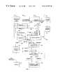
- FIG. 1is a block diagram of a graphics sub-system in accordance with one embodiment of the present invention.
- FIG. 2is a schematic diagram illustrating the logical division of an embedded DRAM memory and a system memory in a 3-D graphics acceleration mode in accordance with one embodiment of the present invention.
- FIG. 3is a block diagram of a graphics sub-system in accordance with another embodiment of the present invention.
- FIG. 4is a block diagram illustrating an embedded DRAM memory used in a graphics sub-system in accordance with one embodiment of the present invention.
- FIG. 5is a circuit diagram of the column structure of a memory bank in accordance with one embodiment of the present invention.
- FIG. 6is a schematic diagram an embedded DRAM memory in accordance with one embodiment of the present invention.
- FIG. 7Ais a waveform diagram illustrating various signals of the access control circuitry of FIG. 6 for four consecutive bank conflict accesses.
- FIG. 7Bis a waveform diagram illustrating various signals of the access control circuitry of FIG. 6 for four consecutive non-conflict bank accesses.
- FIG. 1is a block diagram of a graphics sub-system 100 in accordance with one embodiment of the present invention.
- graphics sub-system 100accelerates the rendering of raster graphics for both 2-D and 3-D applications.
- Graphics sub-system 100includes system interface 101 , 2-D graphics accelerator 102 , 3-D graphics accelerator 103 , cache controller 104 , cache tag memory 105 , comparator 106 , external memory control 107 , display controller 108 and multi-bank embedded dynamic random access memory (DRAM) 110 .
- graphics sub-system 100is fabricated on a single integrated circuit chip.
- Graphics sub-system 100is coupled to external circuitry, including an external frame buffer memory 109 , a system memory 112 , system logic 113 and a video display terminal 114 .
- external circuitryincluding an external frame buffer memory 109 , a system memory 112 , system logic 113 and a video display terminal 114 .
- System interface 101provides a connection to a system bus 111 , thereby enabling graphics sub-system 100 to receive data and address information from system memory 112 through system logic 113 .
- system interface 101 and system bus 111observe the specifications of AGP (Accelerated Graphics Port Interface Specification, Rev. 1.0, Intel Corporation, Jul. 31st, 1996).
- graphics sub-system 100is configured to operate in either a 2-D graphics accelerator mode or a 3-D graphics accelerator mode. Under normal operations, 2-D accelerator 102 and 3-D accelerator 103 are never operating simultaneously. When graphics sub-system 100 is operating as in the 2-D graphics accelerator mode, 2-D accelerator 102 is enabled, and 3-D graphics accelerator 103 is disabled. Conversely, when graphics sub-system 100 is operating in the 3-D graphics accelerator mode, 3-D accelerator 103 is enabled, and 2-D graphics accelerator 102 is disabled.
- embedded DRAM 110when graphics sub-system 100 is in the 2-D graphics accelerator mode, embedded DRAM 110 is operated as a display frame buffer or as a temporary off-screen temporary storage location.
- embedded DRAM 110is operated as a cache memory for 3-D graphics accelerator 103 , thereby providing fast access to the most frequently or most recently accessed texture, and other data necessary for 3-D rendering. In the absence of such a cache memory, this data is normally stored in system memory 112 , and is accessed through system interface 101 .
- System interface 101operably couples system bus 111 to a 2-D bus, a 512-bit wide internal data bus SDQ, and a 21-bit wide internal address bus SMA.
- the 2-D busis further coupled to 2-D graphics accelerator 102 .
- the 2-D busis used to transfer data, address and control information to 2-D graphics accelerator 102 .
- Data bus SDQ and address bus SMAare coupled to cache controller 104 .
- data values SDQ[ 511 : 0 ]are transferred between cache controller 104 and system bus 111 through data bus SDQ and system interface 101 .
- address signals SMA[ 26 : 6 ]are transferred from cache controller 104 to system bus 111 through address bus SMA and system interface 101 .
- cache controller 104is able to control data transfer from system memory 112 to 3-D accelerator 103 and embedded DRAM memory 110 .
- Cache controller 104is further coupled to a 512-bit wide data bus MDQ and a 16-bit wide address bus MDA.
- Data bus MDQ and address bus MDAare also coupled to 2-D graphics accelerator 102 , embedded DRAM memory 110 and display controller 108 .
- Data bus MDQ and address bus MDAcarry data signals MDQ[ 511 : 0 ] and address signals MA[ 21 : 6 ], respectively, in a manner described in more detail below.
- Cache controller 104is also coupled to cache tag memory 105 and comparator 106 by a 14-bit address bus A, a 1-bit update control line and a 1-bit hit control line.
- Cache tag memory 105 and comparator 106are coupled by a 6-bit address bus CT. More specifically, address signals A[ 26 : 21 ] are routed from cache controller 104 to cache tag memory 105 and comparator 106 on address bus A. Address signals A[ 20 : 12 ] are routed from cache controller 104 to cache tag memory 105 on address bus A. An UPDATE control signal is routed from cache controller 105 to cache tag 105 on the update control line, and a HIT control signal is routed from comparator 106 to cache controller 104 on the hit control line.
- a 6-bit cache address CT[ 5 : 0 ]is routed from cache tag memory 105 to comparator 106 . The operation of cache controller 104 , cache tag memory 105 and comparator 106 are described in more detail below.
- Cache controller 104is also coupled to 3-D graphics accelerator 103 by 512-bit wide data bus 3 DQ and 21-bit wide address bus 3 MA.
- Data bus 3 DQ and address bus 3 MAcarry data signals 3 DQ[ 512 : 0 ] and address signals 3 MA[ 26 : 6 ], respectively, in a manner described in more detail below.
- 3-D graphics accelerator 103is further coupled to a 64-bit wide data bus XDQ and a 20-bit wide address bus XDA.
- Data bus XDQ and address bus XDAare also coupled to external memory control 107 and display controller 108 .
- Data bus XDQ and address bus XDAcarry data signals XDQ[ 63 : 0 ] and address signals XMA[ 22 : 3 ], respectively, in a manner described in more detail below.
- External memory controller 107is further coupled to external frame buffer memory 109 by a 64-bit wide data bus EDQ and a 20-bit wide address bus EMA.
- Data bus EDQ and address bus EDAcarry data signals EDQ[ 63 : 0 ] and address signals EMA[ 22 : 3 ], respectively, in a manner described in more detail below.
- 3-D graphics accelerator 103is a conventional circuit that accesses data values stored in system memory 112 or in embedded DRAM memory 110 .
- 3-D graphics accelerator 103processes these data values in accordance with well-known processing techniques, thereby generating a plurality of display data values that represent frames of video information.
- These display data valuesare stored in external frame buffer memory 109 under the control of external memory controller 107 .
- External frame buffer memory 109typically stores one to two frames of display data values.
- 64-bit display data valuesare routed from 3-D graphics accelerator 103 to external memory controller 107 on data bus XDQ, with the address values associated with these display data values are routed on address bus XMA.
- External memory controller 107then transmits these display data values and associated address values to external frame buffer memory 109 on data bus EDQ and address bus EMA.
- Display controller 108retrieves display data values from external frame buffer memory 109 (through external memory controller 107 ) and transmits these display data values to video display terminal 114 , thereby controlling the screen refresh operation. Display data values are transmitted from external frame buffer memory 109 to display controller 108 on data buses XDQ and EDQ. Similarly, address values are transferred between external frame buffer memory 109 and display controller 108 on address buses XMA and EMA.
- external frame buffer memory 109is implemented in system memory 112 and display controller 108 accesses system memory 112 through system interface 101 and the on-chip system bus, which includes data bus SDQ and address bus SMA.
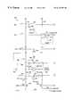
- FIG. 2is a schematic diagram illustrating the logical division of embedded DRAM memory 110 and system memory 112 in the 3-D mode in accordance with one embodiment of the present invention.
- embedded DRAM memory 110has a capacity of 2.5 Mbytes, which is provided by 20 DRAM banks.
- 2 Mbytes (2 21 bytes or 16 banks) of embedded DRAM memory 110is used as cache memory (and the remaining 0.5 Mbyte is unused).
- the 2 Mbyte cache memoryis divided into 512 cache pages, each cache page having 4 Kbytes. These cache pages (Cache_Page — 0-Cache_Page — 511) are illustrated in FIG. 2 .
- system memory 112has a maximum capacity of 128 Mbytes (2 27 bytes).
- the cache systemuses direct mapping.
- system memory 112is divided into 512 sections (Section — 0-Section — 511).
- Each sectionhas 64 blocks (i.e., Block — 0-Block — 63), with each block having a capacity of 4 Kbytes.
- Each cache pagetherefore has the same capacity as each system memory block.
- Each cache pagecorresponds with one of the sections in system memory 112 .
- Cache_Page — 0corresponds with Section — 0
- Cache_Page — 1corresponds with Section — 1.
- Each cache pagestores data from one of the 64 blocks in its corresponding section.
- Cache_Page — 0stores data from one of the 64 blocks in Section —
- Cache_Page — 1stores data from one of the 64 blocks in Section — 1.
- Cache tag memory 105includes 512 entries, each of these entries being associated with a corresponding one of the 512 cache pages. Each entry of cache tag memory 105 contains two fields: a 6-bit address field and a 1-bit valid field. The address field is 6-bits wide, thereby enabling each entry to identify the block associated with the cache page. For example, if Cache_Page — 0 is storing the data of Block — 2 of Section — 0, then the cache tag entry associated with Cache_Page — 0 would store a 6-bit value equal to “000010”, or a binary “2” value, thereby identifying Block — 2. The valid bit indicates whether the current entry is valid. During system reset, the valid bit of each entry is reset to zero, thereby invalidating all the cache entries.
- 3-D accelerator 103transmits a system memory address 3 MA[ 26 : 6 ] associated with the desired data values to cache controller 104 on address bus 3 MA. Bits 3 MA[ 20 : 12 ] correspond with the section of system memory 112 to be accessed. Bits 3 MA[ 26 : 21 ] correspond with the block to be accessed within the addressed section. 3-D accelerator 103 also transmits a control signal (not shown), that indicates to cache controller 104 that the desired access is a read access. In response, cache controller 104 accesses cache tag memory 105 to determine whether a cache hit or a cache miss occurs.
- cache controller 104accesses system memory 112 by transmitting the address signals 3 MA[ 26 : 6 ] to system memory 112 as address signals SMA[ 26 : 6 ].
- System memory 112accesses the addressed section and block in response to address signals SMA[ 26 : 6 ].
- address signals SMA[ 26 : 6 ]identify Section — 2, Block — 8 of system memory 112 .
- all of the data values in Section — 2, Block — 8are transmitted from system memory 112 , through system interface 101 , to cache controller 104 .
- Cache controller 104transmits these data values to embedded DRAM memory 110 on data bus MDQ.
- Embedded DRAM memory 110stores these data values in Cache_Page — 2.
- Cache controller 104also provides the requested data values to 3-D graphics accelerator 103 .
- cache controller 104provides the address signals representative of Cache_Page — 2 to cache tag memory 105 (as address signals A[ 20 : 12 ]). Cache controller also provides the address signals identifying Block — 8 to cache tag memory 105 (as address signals A[ 26 : 21 ]). Cache controller 104 further asserts the UPDATE signal, thereby causing the address signals identifying Block — 8 to be written to the address field of the cache tag entry corresponding to Cache_Page — 2, and setting the associated valid bit to a logic “1” value. At this time, cache tag memory 105 stores information that identifies the contents of embedded DRAM memory 110 .
- Cache controller 104accesses embedded DRAM memory 110 as follows.
- 3-D graphics controller 103provides an address 3 MA[ 26 : 6 ] and a read enable signal to cache controller 104 .
- address signals SMA[ 26 : 6 ]identify Section — 2, Block — 8 of system memory 112 .
- Address signals SMA[ 20 : 12 ], which are representative of Section — 2, as well as Cache_Page — 2,are transmitted to cache tag memory 105 .
- cache tag memory 105provides the contents of the cache tag entry corresponding to Cache_Page — 2 to comparator 106 .
- cache tag memory 105provides an address representative of Block — 8.
- Cache controller 104also provides the address values identifying the block requested by the current access (i.e., Block — 8) to comparator 106 as address signals A[ 26 : 21 ]. In response to the matched address signals, comparator 106 asserts the HIT signal, thereby informing cache controller 104 to access embedded DRAM memory 110 instead of system memory 112 .
- cache controller 104first accesses embedded DRAM (cache) memory 110 .
- system memory 112is then accessed.
- Thisis commonly referred as “look-through” arrangement, in which the 3-D accelerator looks through DRAM (cache) memory 110 to system memory 112 .
- look-asideread requests are broadcast to both cache controller 104 and system memory 112 simultaneously.
- datais routed from embedded DRAM memory 110 to 3-D graphics accelerator 103 .
- a write requestis generated to embedded DRAM memory 110 and the data read from system memory 112 is routed to both embedded DRAM memory 110 and 3-D graphics accelerator 103 .
- 3-D graphics accelerator 103also initiates write transfers to system memory 112 or embedded DRAM memory 110 .
- a write-through policyis employed for embedded DRAM memory 110 when this memory is used as a cache memory.
- both embedded DRAM memory 110 and system memory 112are written with the same data simultaneously when there is a cache hit. In case of a cache miss, only system memory 112 is written; no allocation or cache page replacement is carried out.
- Another embodimentimplements a write-back policy, in which write data is written first to embedded DRAM memory 110 irrespective of a cache hit or miss. In case of a miss, a cache page in embedded DRAM memory 110 is allocated for the new data. System memory 112 is updated when the modified cache page is replaced.
- FIG. 3shows another embodiment of the present invention.
- a CPU (Central Processing Unit) interface 302is provided to facilitate the communication between a CPU 301 and system memory 112 , with embedded DRAM memory 110 serving as a cache to system memory 112 .
- embedded DRAM memory 110is a common unified cache memory that is shared between CPU 301 and 3-D graphics accelerator 103 .
- One advantage of a unified cache memoryis that the data in the cache memory is inherently coherent to both CPU 301 and 3-D graphics accelerator 103 .
- Another advantage of this configurationis that CPU 301 and 3-D graphics accelerator 103 can share the tasks of 3-D rendering.
- 3-D graphics accelerator 103is disabled, 2-D graphics accelerator 102 is enabled, and embedded DRAM memory 110 is used as a frame buffer memory for 2-D graphics accelerator 102 , or as a temporary off-screen temporary storage location.
- 2-D graphics accelerator 102is a conventional circuit that accesses data values stored in system memory 112 or in embedded DRAM memory 110 .
- 2-D graphics accelerator 102processes these data values in accordance with well-known processing techniques, thereby generating a plurality of display data values that represent frames of video information. These display data values are stored in embedded DRAM memory 102 under the control of 2-D graphics accelerator 102 .
- embedded DRAM memory 110typically stores one frame of display data values.
- 512-bit display data valuesare routed from 2-D graphics accelerator 102 to embedded DRAM memory 110 on data bus MDQ, with the address values associated with these display data values being routed on address bus MA.
- Display controller 108retrieves display data values from embedded DRAM memory 110 and transmits these display data values to video display terminal 114 , which may include color look-up-tables and video DACs, thereby controlling the creen refresh operation.
- Display data valuesare transmitted from embedded DRAM memory 110 to display controller 108 on data bus MDQ.
- address valuesare transferred between embedded DRAM memory 110 and display controller 108 on address bus MA.
- FIG. 4is a block diagram illustrating embedded DRAM memory 110 .
- Embedded DRAM memory 110includes twenty banks, B 0 to B 19 , twenty access control circuits AC 0 to AC 19 , input/output interface 401 and conflict control circuit 402 .
- Each bankhas an associated access control circuit.
- banks B 0 -B 19are associated with access control circuits AC 0 -AC 19 , respectively.
- Conflict control circuit 402controls access control circuits AC 0 -AC 19 in the manner described below.
- Each of banks B 0 -B 19includes a 1 Mbit array of DRAM cells arranged in 256 rows and 4096 columns.
- the entire capacity of banks B 0 -B 19are used (i.e., 20 Mbits, or 2.5 Mbytes).
- the capacity of banks B 0 -B 15are used (i.e., 16 Mbits, or 2 Mbytes).
- the address unitis 1 byte
- the word size of embedded DRAM 110is 32 bytes
- the word size of system memory 112is 8 bytes.
- Byte level write operations to embedded DRAM memory 110 and system memory 112are controlled using byte mask address signals (not shown).
- these byte mask address signalsare the lower 6 address bits [ 5 : 0 ] of address signals SMA[ 26 : 6 ], 3 MA[ 26 : 6 ] and MA[ 21 : 6 ].
- embedded DRAM memory 110is its inherently large data bandwidth as illustrated by the 512 bit data bus MDQ, which connects the embedded memory to the other functional blocks.
- Each of access control circuits AC 0 -AC 19has its own address latches, a bank identification register which contains the bank identification, and memory control timing sequencer so that each of the associated banks B 0 -B 19 can operate independent of the other banks. All of the memory banks B 0 -B 19 share a common data bus MDQ.
- FIG. 5is a circuit diagram illustrating a column structure 500 of an exemplary memory bank.
- Column structure 500includes bit lines 501 and 502 , word lines 511 and 512 , memory cell transistors 521 - 522 , memory cell capacitors 523 - 524 , equalization line 515 , equalization transistor 516 , sense amplifier control lines 531 - 534 , column switch line 535 , data lines 536 - 537 , sense amplifier transistors 540 - 545 , column select transistors 546 - 547 , and sense amplifier equalization transistor 551 .
- Transistor 521 and capacitor 523form memory cell 561
- transistor 522 and capacitor 524form memory cell 562 , as illustrated.
- Transistors 541 - 544are connected to form regenerative latches which are used as a sense amplifier 550 .
- Sense amplifier 550is coupled to voltage supplies V cc and ground through transistors 540 and 545 , respectively.
- Column structure 500is accessed in a self-timed manner in response to a clock signal, a row access signal RAS#, a row address signal, a column address signal, and a bank address signal.
- the bank addressis compared with the bank identification number in the bank identification register. A match in the comparison causes the row and column addresses to be latched in an address latch.
- the RAS# signalis sampled on each rising edge of the clock signal.
- the normally high equalization signal EQ on equalization line 515is driven to a logic low voltage, thereby turning off both bit line equalization transistor 516 and sense amplifier equalization transistor 551 .
- the row address signalis decoded.
- word line signal WL 0is asserted high, thereby turning on word line 511 (assuming that the row address signal corresponds with word line 511 ).
- a voltage differentialis developed across bit lines 501 and 502 .
- Sense amplifier signals SA and SA#are asserted high and low, respectively, in response to the subsequent falling edge of the clock signal, thereby activating sense amplifier 550 .
- the activation of sense amplifier 50causes the data value on bit lines 501 and 502 to be latched in sense amplifier 50 .
- the column address decoding operationis initiated by the next rising edge of the clock signal.
- a column switch signal CSWis asserted high, thereby turning on transistors 546 and 547 (assuming that column structure 500 is identified by the column address signal).
- the addressed datais provided on complementary data lines 536 and 537 .
- the complimentary data lines 536 and 537are connected to seven other column structures similar to column structure 500 . These seven other column structures are controlled by seven other column select signals, thereby forming an 8-to-1 column multiplexer. This 8-to-1 column multiplexer allows 512 of the 4096 columns of a bank to be selected. As described in more detail below, complementary data lines 536 and 537 are connected to input/output interface 401 .
- column structure 500takes three clock cycles to complete. That is, memory cycle time equals 3 clock periods.
- Each of memory banks B 0 -B 19generates its own timing signals EQ, SA, and CSW in the manner described above.
- the RAS# signalis generated by conflict control circuit 402 in the manner described below.
- the operation of column structure 500is described in more detail in U.S. Pat. No. 5,675,169, which is hereby incorporated by reference.
- FIG. 6is a schematic diagram of embedded DRAM memory 110 in accordance with one embodiment of the invention.
- Input/output interface 401includes data amplifier 601 , read latches 602 , write driver 603 , write latches 604 and bus transceiver 605 .
- Conflict control circuit 402includes address latch 606 , history buffer 607 (which includes registers 607 A and 607 B), comparators 608 - 609 , NOR gate 610 , flip-flops 611 - 612 , inverters 613 - 614 , OR gates 615 - 616 and AND gate 617 .
- Data amplifier 601includes 512 amplifier circuits, which amplify the output signals received from the selected sense amplifiers in embedded DRAM memory 110 .
- Data amplifier 601is coupled to read latches 602 .
- Read latches 602include 512 latches for receiving and storing the data values provided by data amplifier 601 .
- Read latches 602provide 512 output signals to bus transceiver 605 , which in turn, transmits these output signals as data signals MDQ[ 511 : 0 ] on data bus MDQ.
- Write data valuesare provided to bus transceiver 605 on data bus MDQ. These write data values are transmitted from bus transceiver 605 to write latches 604 .
- Write latches 604include 512 latches for storing the write data values received from bus transceiver 605 .
- Write latches 604are coupled to provide the write data values to write driver 603 .
- Write driver 603provides the data values to be written to data amplifier 603 .
- Write driver 603includes 512 tri-state buffers that are controlled by a read/write indicator signal MWE# and a write mask signal MDM[ 63 : 0 ].
- the MWE# signalis driven by a memory client (e.g., 2-D accelerator 102 or 3-D accelerator 103 ) at the beginning of a memory transaction, thereby indicating whether the transaction is a read or a write operation. For a write operation, MWE# is driven low and for a read operation, MWE# is driven high.
- a logic low write enable signal MWE#enables write drivers 603
- the write mask signal MDM[ 63 : 0 ]enables and disables selected tri-state buffers, thereby providing a byte level write capability.
- the tri-state buffers in write driver 603are disabled (i.e., in a high-impedance state) during read operations.
- data amplifier 601is coupled to a pre-fetched read buffer and write driver 603 is coupled to a posted write buffer, in the manner described in commonly owned, co-pending U.S. patent application Ser. No. 08/679,873, which is hereby incorporated by reference.
- the pre-fetched read bufferis coupled to a bus receiver that connects to a 128-bit read data bus.
- the posted write bufferis coupled to a bus driver that connects to a 128-bit write data bus.
- the read and write data busesare uni-directional and they couple embedded DRAM memory 110 to the other functional blocks.
- the data transfer frequency of the read and write data busesis twice that of the 512-bit bi-directional bus internal to the memory array.
- One advantage of an embodiment using dedicated read and write busesis the that timing overhead associated with bus turn-around is avoided.
- address latch 606is coupled to receive address signals MA[ 21 : 6 ] from address bus MA.
- Address latch 606is also coupled to receive an address strobe signal LAT and a clock signal CLK.
- the address strobe signal LATis generated in response to an external address strobe signal MADS# and a internal match signal MCH#.
- the address strobe signal MADS#informs memory 110 of the presence of a new memory transaction.
- the address signals MA[ 21 : 6 ]are loaded into address latch 606 as latched address signals LA[ 16 : 6 ] in response to a logic low address strobe signal LAT, and a rising edge of the clock signal CLK.
- the memory addressis mapped as follows: LA[ 21 : 17 ] identifies the bank address, LA[ 16 : 9 ] identifies the row address, and LA[ 8 : 6 ] identifies the column address.
- the clock signal CLK, row access signal RAS# and latched address signals LA[ 21 : 6 ]are provided to the access control circuits AC 0 -AC 19 . In response, these access control signals generate the appropriate access signals as described above in connection with FIG. 5 .
- embedded DRAM memory 110receives all the addresses (i.e., bank, row, column) in the same clock cycle. As described above, address latch 606 latches these addresses at the rising edge of the CLK signal when the LAT signal is detected low.
- Each of memory banks B 0 -B 19has its own access control circuit, thereby facilitating parallel multi-bank operations in which one bank is in the row address decoding state, another bank is in the read or write state, and yet another bank is in the beginning of the pre-charge state. Operating banks B 0 -B 19 in parallel allows pipelined random accessing to different banks.
- Non-conflicting bank accessesoccur as long as none of the accesses within a three clock cycle period are addressed to the same bank. If the same bank is accessed more than once during any three clock cycle period, a bank-conflict exists because the accessed bank is not ready for handling the row access. Consequently, consecutive accesses to any one bank are not allowed unless the accesses are separated by three clock cycles or longer.
- bank B 0if bank B 0 is accessed at clock cycle n, then bank B 0 cannot begin to perform another access transaction until beginning of clock cycle n+3. Since the embedded DRAM memory 110 consists of 20 banks (16 banks during 3-D mode) and the cycle time of each individual memory bank is 3 clock cycles, the probability of bank conflict (accesses to the same bank within 3 clock cycles), is approximately 3/20 or 15%. Therefore, the average access cycle time for the memory is (0.15 ⁇ 3)+0.85 clock cycles, or 1.3 clock cycles.
- Embedded DRAM memory 110therefore behaves very much like a synchronous SRAM which can support close to one random access per clock cycle.
- conflict control circuit 402responds to non-conflict accesses and bank conflict accesses as follows.
- the latched address signal LA[ 21 : 17 ]is stored in register 607 A of history buffer 607 on the following falling edge of the CLK signal after the RAS# signal is detected low.
- the address signal previously stored in register 607 Ais transferred to register 607 B of history register 607 .
- history buffer 607is a two entry first in, first out (FIFO) memory.
- address latch 606 , register 607 A and register 607 Brepresent the access addresses of a current access, an access occurring one memory cycle ago, and an access occurring two memory cycles ago, respectively. If the contents of address latch 606 match the contents of register 607 A, then the current access is directed to the same bank as the previous access (bank-conflict), and the current access must be delayed for at least two clock cycles. Similarly, if the contents of address latch 606 match the contents of register 607 B, then the current access is directed to the same bank as the access occurring two memory cycles ago, and the current access must be delayed for at least one clock cycle.
- Comparator 608is coupled to receive the addresses stored in address latch 606 and register 607 A.
- Comparator 609is coupled to receive the addresses stored by address latch 606 and register 607 B.
- comparators 608 and 609Upon detecting a match, comparators 608 and 609 assert logic high signals, which are applied to NOR gate 610 .
- NOR gate 610asserts a logic low match signal MCH# when either of comparators 608 and 609 asserts a logic high signal.
- the logic low match signal MCH#therefore indicates that a bank conflict transaction is pending.
- the logic low MCH# signalis used to delay access to DRAM memory 110 , when required.
- the logic low MCH# signalis latched into flip flop 611 in response to the rising edge of the CLK signal.
- flip flop 611provides a logic high ready control signal RDY# at its Q# output terminal.
- the logic high RDY# signalindicates to the accessing client (e.g., 2-D graphics accelerator 102 or 3-D graphics accelerator 103 ) that DRAM memory 110 is not yet ready for any further accesses.
- the system accessing DRAM arraye.g., 2-D accelerator 102 or 3-D accelerator 103
- the logic low RDY# signalindicates that memory 110 is ready to receive another access transaction, that the requested read data is provided, or that new write data should be gated in.
- the logic low MCH# signalis also provided to inverter 613 and flip flop 612 .
- the logic low MCH# signalis loaded into flip flop 612 in response to the falling edge of the CLK signal.
- inverter 613provides a logic high signal to OR gate 615 .
- OR gate 615provides a logic high value to AND gate 617 .
- the logic low MCH# signalis also applied to inverter 614 .
- the output signal of inverter 614is provided to an input terminal of OR gate 616 .
- the other input terminal of OR gate 616is coupled to receive the address strobe signal MADS#.
- the output terminal of OR gate 616is coupled to the other input terminal of AND gate 617 .
- the logic low MCH# signalensures that OR gate 616 provides a logic high signal to AND gate 617 .
- the RAS# signal provided by AND gate 617is maintained at a logic high level, thereby preventing further read accesses to DRAM memory 110 . Note that as long as the MCH# signal stays low, the RAS# signal remains high.
- the first conditionexists when the MADS# signal is low and the MCH# signal is high. During the first condition, no pending transactions are queued up.
- the second conditionexists when the MCH# signal undergoes a transition from low to high, thereby signaling the queued up transaction is beginning to be executed.
- the MCH# signaltransitions to a logic high value.
- This logic high MCH# signalis latched into flip flop 611 in response to the next rising edge of the CLK signal, thereby asserting a logic low RDY# signal and alerting the accessing device to initiate the next access.
- a mechanismis required to assert the RAS# signal 612 low, so as to start the execution of the queued up bank-conflict transaction whose address is stored in address latch 606 .
- This mechanismis provided by a one-shot circuit 620 , that consists of inverter 613 , flip flop 612 and OR gate 615 .
- the one-shot circuit 620generates a negative pulse of one clock cycle on its output upon the detection of a low-to-high transition on the MCH# signal.
- the original logic low MCH# signalis stored in flip flop 612 .
- the output of inverter 613becomes a logic low state.
- the logic high MCH# signalalso enables the MADS# signal to control the state of the RAS# signal.
- a logic high MADS#will cause the RAS# signal to remain high. Such is the case as the RDY# signal does not go low until the next rising edge of the CLK signal.
- the accessing clientdoes not drive the MADS# signal low until the next clock cycle.
- the RAS# signalis asserted low by the output of one-shot circuit 620 until the next falling edge of the CLK signal.
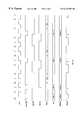
- FIG. 7Ais a waveform diagram illustrating various signals of conflict control circuit 402 for four consecutive bank conflict accesses.
- memory 110is ready to receive a new transaction, with the RDY# signal asserted low.
- an accessing clientfor example display controller 108 , asserts a logic low MADS# signal, drives a first access address MA 1 [ 21 : 6 ] onto address bus MA, and drives the MWE# signal to the desired state (MWE 1 ).
- the low MADS# signal and the high MCH# signalresults in a low LAT signal.
- the low LAT signal and the low CLK signalcause address latch 606 to enter a transparent state, such that the first address MA 1 [ 21 : 6 ] is gated to the internal address bus as first internal address LA 1 [ 21 : 6 ].
- the first address MA 1 [ 21 : 6 ]is latched into address latch 606 on the rising edge of the CLK signal.
- the upper five address bits of LA 1 [ 21 : 17 ]i.e., the bank address
- each of registers 607 A and 607 Bstores an address of a bank currently being accessed.
- the contents of registers 607 A and 607 Bare shifted downward on each falling edge of the CLK signal.
- Register 607 Astores a bank address received from address latch 606 on the falling edge of the CLK signal when a new memory cycle begins, as indicated by a logic low RAS# signal.
- the address latched in register 607 Ais advanced to register 607 B on the next falling edge of the clock signal, and is flushed out of register 607 B on the next falling edge of the CLK signal. Therefore, the bank address of any transaction stays in history buffer 607 for two clock cycles.
- register 607 AWhen there is no new transaction, as indicated by a logic high RAS# signal, the contents of register 607 A are set to all high values (i.e., 11111). Since there is no bank with this address, a new bank address received from address latch 606 will not result in a match.
- Each of the access control circuits AC 0 -AC 19 of memory 110compares its own unique pre-coded bank identity address with the current the bank address LA 1 [ 21 : 6 ] stored in address latch 606 .
- the access control circuit that detects a matchtriggers a memory access in response to the low RAS# signal and the rising edge of the CLK signal at the beginning of cycle T 1 .
- the first bank address LA 1 [ 21 : 17 ]is latched in register 607 A of history buffer 607 .
- the low RDY# signalinforms the accessing client that the read data is available at the end of next clock cycle T 2 (illustrated as RD 1 in FIG.
- the low RDY# signal during clock cycle T 1also indicates to the next accessing client that a new memory transaction can begin.
- the next accessing clientcan be the same or different from the initial accessing client.
- the client of the first transactioncan be display controller 108
- the client of the second transactioncan be either 2-D accelerator 102 or display controller 108 .
- the next accessing clientbegins the second transaction by driving the MADS# signal low, the MWE# signal to the desired state and the second memory address MA 2 [ 21 : 6 ] on address bus MA.
- the second memory address MA 2 [ 21 : 6 ]is routed through address latch 606 (which is transparent at this time), as second memory address LA 2 [ 21 : 6 ].
- the addressis checked against those in the history buffer.
- the second memory address LA 2 [ 21 : 6 ] transactionaccesses the same bank as the first memory address LA 1 [ 21 : 6 ].
- comparator 608detects a match between the first bank address (stored in register 607 A during the first cycle T 1 ) and the second bank address (provided by address latch 606 ).
- comparator 608asserts a logic high signal, which in turn, causes NOR gate 610 to assert a logic low MCH# signal.
- the logic low MCH# signalindicates that the addressed bank is busy.
- the low MCH# signalis latched into flip flop 611 , thereby causing the RDY# signal to be de-asserted high.
- the logic high RDY# signalindicates to the accessing clients that memory 110 is busy and cannot be accessed. Even though the first memory access is completed at the end of cycle T 2 , the memory cycle in the addressed bank is not finished until the end of cycle T 3 because the memory bank takes one clock cycle to pre-charge before a new memory cycle can start.
- the first bank address LA 1 [ 21 : 17 ]is not cleared from history buffer 607 until the falling edge of the CLK signal during cycle T 3 .
- the MCH# signalgoes high, thereby signaling that operations in the first addressed bank will be finished at the end of this cycle.
- the rising edge the MCH# signalcauses the one-shot circuit, formed by inverter 613 , flip flop 612 and OR gate 615 to drive the output of OR gate 615 low for one clock cycle. This in turn causes the RAS# signal to go low for one clock cycle.
- the low RAS# signal and the second address LA 2 [ 21 : 6 ]cause a new memory cycle to begin.
- FIG. 7Bis a waveform diagram illustrating various signals of conflict control circuit 402 for four consecutive non-conflict bank accesses.
- the first three transactionsaccess different banks, and the fourth transaction accesses the same bank as the first transaction. Because the memory bank accessed during the first cycle T 1 has completed its memory cycle at the end of cycle T 3 , this memory bank is able to handle the fourth transaction (which begins during cycle T 4 ) without delay. Because the first three transactions address different banks, no bank conflict exists, and the transactions are processed in consecutive clock cycles without delay.
- the access timeis equal to memory cycle time (3 clock cycles) plus memory access time (2 clock cycles) minus 1 clock cycle, which is equal to four clock cycles.
- the access timeis two clock cycles, but the memory can process one access per clock because of the multi-bank operation scheme. Since memory 110 has an access time varying from 2 clock cycles to 4 clock cycles, a handshake mechanism is incorporated for synchronizing the transactions and data transfers. The ready control signal RDY# is used to implement this handshake mechanism in the manner described above.
- the embedded DRAM and system memorycan have different sizes in different embodiments.
- the embedded DRAMcan have different numbers of memory banks.
- buses having different widths than those describedcan be used in other embodiments.
Landscapes
- Physics & Mathematics (AREA)
- General Physics & Mathematics (AREA)
- Engineering & Computer Science (AREA)
- Theoretical Computer Science (AREA)
- Dram (AREA)
Abstract
Description
Claims (22)
Priority Applications (1)
| Application Number | Priority Date | Filing Date | Title |
|---|---|---|---|
| US09/133,475US6215497B1 (en) | 1998-08-12 | 1998-08-12 | Method and apparatus for maximizing the random access bandwidth of a multi-bank DRAM in a computer graphics system |
Applications Claiming Priority (1)
| Application Number | Priority Date | Filing Date | Title |
|---|---|---|---|
| US09/133,475US6215497B1 (en) | 1998-08-12 | 1998-08-12 | Method and apparatus for maximizing the random access bandwidth of a multi-bank DRAM in a computer graphics system |
Publications (1)
| Publication Number | Publication Date |
|---|---|
| US6215497B1true US6215497B1 (en) | 2001-04-10 |
Family
ID=22458790
Family Applications (1)
| Application Number | Title | Priority Date | Filing Date |
|---|---|---|---|
| US09/133,475Expired - Fee RelatedUS6215497B1 (en) | 1998-08-12 | 1998-08-12 | Method and apparatus for maximizing the random access bandwidth of a multi-bank DRAM in a computer graphics system |
Country Status (1)
| Country | Link |
|---|---|
| US (1) | US6215497B1 (en) |
Cited By (76)
| Publication number | Priority date | Publication date | Assignee | Title |
|---|---|---|---|---|
| US6362824B1 (en)* | 1999-01-29 | 2002-03-26 | Hewlett-Packard Company | System-wide texture offset addressing with page residence indicators for improved performance |
| US20020154130A1 (en)* | 2001-04-18 | 2002-10-24 | Minoru Niimura | Liquid crystal display apparatus |
| US20020174252A1 (en)* | 2001-05-18 | 2002-11-21 | Broadcom Corporaion | System on a chip for packet processing |
| US20030001852A1 (en)* | 2000-11-12 | 2003-01-02 | Tuomi Mika Henrik | 3-D rendering engine with embedded memory |
| US20030001687A1 (en)* | 2001-01-31 | 2003-01-02 | Compaq Computer Corporation | Single to differential interfacing |
| US6532018B1 (en)* | 1999-04-19 | 2003-03-11 | Microsoft Corporation | Combined floating-point logic core and frame buffer |
| US6549042B2 (en)* | 2000-06-23 | 2003-04-15 | Integrated Device Technology, Inc. | Complementary data line driver circuits with conditional charge recycling capability that may be used in random access and content addressable memory devices and method of operating same |
| US6574708B2 (en)* | 2001-05-18 | 2003-06-03 | Broadcom Corporation | Source controlled cache allocation |
| US6598116B1 (en)* | 1998-11-02 | 2003-07-22 | Nokia Mobile Phones Limited | Memory interface using only one address strobe line |
| US6606680B2 (en)* | 2001-06-29 | 2003-08-12 | International Business Machines Corporation | Method and apparatus for accessing banked embedded dynamic random access memory devices |
| US6614449B1 (en)* | 1998-08-28 | 2003-09-02 | Ati International Srl | Method and apparatus for video graphics antialiasing using a single sample frame buffer and associated sample memory |
| US6618048B1 (en) | 1999-10-28 | 2003-09-09 | Nintendo Co., Ltd. | 3D graphics rendering system for performing Z value clamping in near-Z range to maximize scene resolution of visually important Z components |
| US20030169626A1 (en)* | 2002-03-06 | 2003-09-11 | Burk Wayne Eric | System and method for controlling a number of outstanding data transactions within an integrated circuit |
| US6636214B1 (en) | 2000-08-23 | 2003-10-21 | Nintendo Co., Ltd. | Method and apparatus for dynamically reconfiguring the order of hidden surface processing based on rendering mode |
| US20030217235A1 (en)* | 2002-05-15 | 2003-11-20 | Broadcom Corporation | Ambiguous virtual channels |
| US20030217238A1 (en)* | 2002-05-15 | 2003-11-20 | Broadcom Corporation | Data pend mechanism |
| US6674441B1 (en)* | 2000-07-26 | 2004-01-06 | Ati International, Srl | Method and apparatus for improving performance of an accelerated graphics port (AGP) device |
| US6690379B2 (en) | 1997-07-01 | 2004-02-10 | Memtrax Llc | Computer system controller having internal memory and external memory control |
| US6700586B1 (en) | 2000-08-23 | 2004-03-02 | Nintendo Co., Ltd. | Low cost graphics with stitching processing hardware support for skeletal animation |
| US20040044806A1 (en)* | 2002-05-15 | 2004-03-04 | Moll Laurent R. | Addressing scheme supporting variable local addressing and variable global addressing |
| US6707458B1 (en) | 2000-08-23 | 2004-03-16 | Nintendo Co., Ltd. | Method and apparatus for texture tiling in a graphics system |
| US6717577B1 (en) | 1999-10-28 | 2004-04-06 | Nintendo Co., Ltd. | Vertex cache for 3D computer graphics |
| US6766389B2 (en) | 2001-05-18 | 2004-07-20 | Broadcom Corporation | System on a chip for networking |
| US6779076B1 (en) | 2000-10-05 | 2004-08-17 | Micron Technology, Inc. | Method and system for using dynamic random access memory as cache memory |
| US6784892B1 (en)* | 2000-10-05 | 2004-08-31 | Micron Technology, Inc. | Fully associative texture cache having content addressable memory and method for use thereof |
| US20040186957A1 (en)* | 2000-08-17 | 2004-09-23 | Brent Keeth | Method and system for using dynamic random access memory as cache memory |
| US6801207B1 (en) | 1998-10-09 | 2004-10-05 | Advanced Micro Devices, Inc. | Multimedia processor employing a shared CPU-graphics cache |
| US6809737B1 (en)* | 1999-09-03 | 2004-10-26 | Ati International, Srl | Method and apparatus for supporting multiple monitor orientations |
| US6811489B1 (en) | 2000-08-23 | 2004-11-02 | Nintendo Co., Ltd. | Controller interface for a graphics system |
| US20040239372A1 (en)* | 2003-05-30 | 2004-12-02 | Chih-Ming Hung | RF differential signal squarer/limiter and balancer with high power supply rejection |
| US6842180B1 (en)* | 2000-09-20 | 2005-01-11 | Intel Corporation | Opportunistic sharing of graphics resources to enhance CPU performance in an integrated microprocessor |
| US6867781B1 (en) | 2000-08-23 | 2005-03-15 | Nintendo Co., Ltd. | Graphics pipeline token synchronization |
| US6867779B1 (en)* | 1999-12-22 | 2005-03-15 | Intel Corporation | Image rendering |
| US6924810B1 (en)* | 1998-10-09 | 2005-08-02 | Advanced Micro Devices, Inc. | Hierarchical texture cache |
| US6937245B1 (en)* | 2000-08-23 | 2005-08-30 | Nintendo Co., Ltd. | Graphics system with embedded frame buffer having reconfigurable pixel formats |
| US7002591B1 (en) | 2000-08-23 | 2006-02-21 | Nintendo Co., Ltd. | Method and apparatus for interleaved processing of direct and indirect texture coordinates in a graphics system |
| US20060047887A1 (en)* | 2004-08-27 | 2006-03-02 | Jeddeloh Joseph M | Memory system and method having unidirectional data buses |
| US7034828B1 (en) | 2000-08-23 | 2006-04-25 | Nintendo Co., Ltd. | Recirculating shade tree blender for a graphics system |
| US7061502B1 (en) | 2000-08-23 | 2006-06-13 | Nintendo Co., Ltd. | Method and apparatus for providing logical combination of N alpha operations within a graphics system |
| US20060197768A1 (en)* | 2000-11-28 | 2006-09-07 | Nintendo Co., Ltd. | Graphics system with embedded frame buffer having reconfigurable pixel formats |
| US7119813B1 (en) | 2000-06-02 | 2006-10-10 | Nintendo Co., Ltd. | Variable bit field encoding |
| US20060250879A1 (en)* | 2005-02-23 | 2006-11-09 | Jeddeloh Joseph M | Memory device and method having multiple internal data buses and memory bank interleaving |
| US20070028027A1 (en)* | 2005-07-26 | 2007-02-01 | Micron Technology, Inc. | Memory device and method having separate write data and read data buses |
| US7184059B1 (en) | 2000-08-23 | 2007-02-27 | Nintendo Co., Ltd. | Graphics system with copy out conversions between embedded frame buffer and main memory |
| US20070067579A1 (en)* | 2005-09-05 | 2007-03-22 | Sony Corporation | Shared memory device |
| US7196710B1 (en) | 2000-08-23 | 2007-03-27 | Nintendo Co., Ltd. | Method and apparatus for buffering graphics data in a graphics system |
| US7205999B2 (en) | 2000-08-23 | 2007-04-17 | Nintendo Co., Ltd. | Method and apparatus for environment-mapped bump-mapping in a graphics system |
| US7245302B1 (en)* | 2003-10-30 | 2007-07-17 | Nvidia Corporation | Processing high numbers of independent textures in a 3-D graphics pipeline |
| US20070168616A1 (en)* | 2001-10-04 | 2007-07-19 | Micron Technology, Inc. | Embedded dram cache memory and method having reduced latency |
| US7307640B2 (en) | 2000-08-23 | 2007-12-11 | Nintendo Co., Ltd. | Method and apparatus for efficient generation of texture coordinate displacements for implementing emboss-style bump mapping in a graphics rendering system |
| US20080112085A1 (en)* | 2006-11-14 | 2008-05-15 | Hitachi Global Technologies Netherlands, B.V. | Write Through Drivers for Disk Drive Systems |
| US20090049325A1 (en)* | 2004-05-28 | 2009-02-19 | Renesas Technology Corp. | Data processor |
| WO2008070576A3 (en)* | 2006-12-01 | 2009-04-30 | Mosys Inc | Embedded memory and multi-media accelerator and method of operating same |
| US7538772B1 (en) | 2000-08-23 | 2009-05-26 | Nintendo Co., Ltd. | Graphics processing system with enhanced memory controller |
| US7688325B1 (en) | 2006-09-21 | 2010-03-30 | Nvidia Corporation | Screen compression for mobile applications |
| US7849208B2 (en) | 2002-08-30 | 2010-12-07 | Broadcom Corporation | System and method for TCP offload |
| US7876327B1 (en) | 2006-12-21 | 2011-01-25 | Nvidia Corporation | Power savings in a computing device during video playback |
| US7912064B2 (en) | 2002-08-30 | 2011-03-22 | Broadcom Corporation | System and method for handling out-of-order frames |
| US7934021B2 (en) | 2002-08-29 | 2011-04-26 | Broadcom Corporation | System and method for network interfacing |
| CN102147722A (en)* | 2011-04-08 | 2011-08-10 | 深圳中微电科技有限公司 | Multithreading processor realizing functions of central processing unit and graphics processor and method |
| US8116203B2 (en) | 2001-07-23 | 2012-02-14 | Broadcom Corporation | Multiple virtual channels for use in network devices |
| US8135016B2 (en) | 2002-03-08 | 2012-03-13 | Broadcom Corporation | System and method for identifying upper layer protocol message boundaries |
| US8180928B2 (en) | 2002-08-30 | 2012-05-15 | Broadcom Corporation | Method and system for supporting read operations with CRC for iSCSI and iSCSI chimney |
| US8195858B1 (en)* | 2009-07-28 | 2012-06-05 | Nvidia Corporation | Managing conflicts on shared L2 bus |
| US8321618B1 (en) | 2009-07-28 | 2012-11-27 | Nvidia Corporation | Managing conflicts on shared L2 bus |
| US8359438B2 (en) | 2010-05-18 | 2013-01-22 | Avago Technologies Enterprise IP (Singapore) Pte. Ltd. | Memory banking system and method to increase memory bandwidth via parallel read and write operations |
| US8402142B2 (en) | 2002-08-30 | 2013-03-19 | Broadcom Corporation | System and method for TCP/IP offload independent of bandwidth delay product |
| US8692837B1 (en) | 2006-09-21 | 2014-04-08 | Nvidia Corporation | Screen compression for mobile applications |
| US8750320B2 (en) | 1997-01-23 | 2014-06-10 | Broadcom Corporation | Fibre channel arbitrated loop bufferless switch circuitry to increase bandwidth without significant increase in cost |
| US8798091B2 (en) | 1998-11-19 | 2014-08-05 | Broadcom Corporation | Fibre channel arbitrated loop bufferless switch circuitry to increase bandwidth without significant increase in cost |
| US20150052304A1 (en)* | 2013-08-19 | 2015-02-19 | Soft Machines, Inc. | Systems and methods for read request bypassing a last level cache that interfaces with an external fabric |
| US9361227B2 (en) | 2013-08-30 | 2016-06-07 | Soft Machines, Inc. | Systems and methods for faster read after write forwarding using a virtual address |
| US9632947B2 (en) | 2013-08-19 | 2017-04-25 | Intel Corporation | Systems and methods for acquiring data for loads at different access times from hierarchical sources using a load queue as a temporary storage buffer and completing the load early |
| US9665468B2 (en) | 2013-08-19 | 2017-05-30 | Intel Corporation | Systems and methods for invasive debug of a processor without processor execution of instructions |
| US10002586B1 (en)* | 2006-12-13 | 2018-06-19 | Nvidia Corporation | Compression of display data stored locally on a GPU |
| US11449432B2 (en)* | 2019-05-24 | 2022-09-20 | Texas Instruments Incorporated | Methods and apparatus for eviction in dual datapath victim cache system |
Citations (5)
| Publication number | Priority date | Publication date | Assignee | Title |
|---|---|---|---|---|
| US5249282A (en) | 1990-11-21 | 1993-09-28 | Benchmarq Microelectronics, Inc. | Integrated cache memory system with primary and secondary cache memories |
| US5949439A (en)* | 1996-08-15 | 1999-09-07 | Chromatic Research, Inc. | Computing apparatus and operating method using software queues to improve graphics performance |
| US6023745A (en)* | 1996-08-08 | 2000-02-08 | Neomagic Corporation | Scoreboarding for DRAM access within a multi-array DRAM device using simultaneous activate and read/write accesses |
| US6026478A (en)* | 1997-08-01 | 2000-02-15 | Micron Technology, Inc. | Split embedded DRAM processor |
| US6032225A (en)* | 1995-12-18 | 2000-02-29 | Texas Instruments Incorporated | Microprocessor system with burstable, non-cacheable memory access support |
- 1998
- 1998-08-12USUS09/133,475patent/US6215497B1/ennot_activeExpired - Fee Related
Patent Citations (5)
| Publication number | Priority date | Publication date | Assignee | Title |
|---|---|---|---|---|
| US5249282A (en) | 1990-11-21 | 1993-09-28 | Benchmarq Microelectronics, Inc. | Integrated cache memory system with primary and secondary cache memories |
| US6032225A (en)* | 1995-12-18 | 2000-02-29 | Texas Instruments Incorporated | Microprocessor system with burstable, non-cacheable memory access support |
| US6023745A (en)* | 1996-08-08 | 2000-02-08 | Neomagic Corporation | Scoreboarding for DRAM access within a multi-array DRAM device using simultaneous activate and read/write accesses |
| US5949439A (en)* | 1996-08-15 | 1999-09-07 | Chromatic Research, Inc. | Computing apparatus and operating method using software queues to improve graphics performance |
| US6026478A (en)* | 1997-08-01 | 2000-02-15 | Micron Technology, Inc. | Split embedded DRAM processor |
Cited By (151)
| Publication number | Priority date | Publication date | Assignee | Title |
|---|---|---|---|---|
| US8767756B2 (en) | 1997-01-23 | 2014-07-01 | Broadcom Corporation | Fibre channel arbitrated loop bufferless switch circuitry to increase bandwidth without significant increase in cost |
| US8774199B2 (en) | 1997-01-23 | 2014-07-08 | Broadcom Corporation | Fibre channel arbitrated loop bufferless switch circuitry to increase bandwidth without significant increase in cost |
| US8750320B2 (en) | 1997-01-23 | 2014-06-10 | Broadcom Corporation | Fibre channel arbitrated loop bufferless switch circuitry to increase bandwidth without significant increase in cost |
| USRE41413E1 (en) | 1997-07-01 | 2010-07-06 | Neal Margulis | Computer system controller having internal memory and external memory control |
| US6690379B2 (en) | 1997-07-01 | 2004-02-10 | Memtrax Llc | Computer system controller having internal memory and external memory control |
| US6614449B1 (en)* | 1998-08-28 | 2003-09-02 | Ati International Srl | Method and apparatus for video graphics antialiasing using a single sample frame buffer and associated sample memory |
| US6924810B1 (en)* | 1998-10-09 | 2005-08-02 | Advanced Micro Devices, Inc. | Hierarchical texture cache |
| US6801207B1 (en) | 1998-10-09 | 2004-10-05 | Advanced Micro Devices, Inc. | Multimedia processor employing a shared CPU-graphics cache |
| US6598116B1 (en)* | 1998-11-02 | 2003-07-22 | Nokia Mobile Phones Limited | Memory interface using only one address strobe line |
| US8798091B2 (en) | 1998-11-19 | 2014-08-05 | Broadcom Corporation | Fibre channel arbitrated loop bufferless switch circuitry to increase bandwidth without significant increase in cost |
| US6362824B1 (en)* | 1999-01-29 | 2002-03-26 | Hewlett-Packard Company | System-wide texture offset addressing with page residence indicators for improved performance |
| US6760033B2 (en) | 1999-04-19 | 2004-07-06 | Microsoft Corporation | Combined floating-point logic core and frame buffer |
| US6532018B1 (en)* | 1999-04-19 | 2003-03-11 | Microsoft Corporation | Combined floating-point logic core and frame buffer |
| US6809737B1 (en)* | 1999-09-03 | 2004-10-26 | Ati International, Srl | Method and apparatus for supporting multiple monitor orientations |
| US6618048B1 (en) | 1999-10-28 | 2003-09-09 | Nintendo Co., Ltd. | 3D graphics rendering system for performing Z value clamping in near-Z range to maximize scene resolution of visually important Z components |
| US6717577B1 (en) | 1999-10-28 | 2004-04-06 | Nintendo Co., Ltd. | Vertex cache for 3D computer graphics |
| US6867779B1 (en)* | 1999-12-22 | 2005-03-15 | Intel Corporation | Image rendering |
| US20050212805A1 (en)* | 1999-12-22 | 2005-09-29 | Intel Corporation | Image rendering |
| US7348986B2 (en) | 1999-12-22 | 2008-03-25 | Intel Corporation | Image rendering |
| US7119813B1 (en) | 2000-06-02 | 2006-10-10 | Nintendo Co., Ltd. | Variable bit field encoding |
| US6549042B2 (en)* | 2000-06-23 | 2003-04-15 | Integrated Device Technology, Inc. | Complementary data line driver circuits with conditional charge recycling capability that may be used in random access and content addressable memory devices and method of operating same |
| US6674441B1 (en)* | 2000-07-26 | 2004-01-06 | Ati International, Srl | Method and apparatus for improving performance of an accelerated graphics port (AGP) device |
| US7917692B2 (en) | 2000-08-17 | 2011-03-29 | Round Rock Research, Llc | Method and system for using dynamic random access memory as cache memory |
| US20040186957A1 (en)* | 2000-08-17 | 2004-09-23 | Brent Keeth | Method and system for using dynamic random access memory as cache memory |
| US20070055818A1 (en)* | 2000-08-17 | 2007-03-08 | Micron Technology, Inc. | Method and system for using dynamic random access memory as cache memory |
| US7155561B2 (en) | 2000-08-17 | 2006-12-26 | Micron Technology, Inc. | Method and system for using dynamic random access memory as cache memory |
| US20060015679A1 (en)* | 2000-08-17 | 2006-01-19 | Brent Keeth | Method and system for using dynamic random access memory as cache memory |
| US6948027B2 (en) | 2000-08-17 | 2005-09-20 | Micron Technology, Inc. | Method and system for using dynamic random access memory as cache memory |
| US7350018B2 (en) | 2000-08-17 | 2008-03-25 | Micron Technology, Inc. | Method and system for using dynamic random access memory as cache memory |
| US6862654B1 (en) | 2000-08-17 | 2005-03-01 | Micron Technology, Inc. | Method and system for using dynamic random access memory as cache memory |
| US20080177943A1 (en)* | 2000-08-17 | 2008-07-24 | Micron Technology, Inc. | Method and system for using dynamic random access memory as cache memory |
| US7061502B1 (en) | 2000-08-23 | 2006-06-13 | Nintendo Co., Ltd. | Method and apparatus for providing logical combination of N alpha operations within a graphics system |
| US7317459B2 (en) | 2000-08-23 | 2008-01-08 | Nintendo Co., Ltd. | Graphics system with copy out conversions between embedded frame buffer and main memory for producing a streaming video image as a texture on a displayed object image |
| US7205999B2 (en) | 2000-08-23 | 2007-04-17 | Nintendo Co., Ltd. | Method and apparatus for environment-mapped bump-mapping in a graphics system |
| US7995069B2 (en) | 2000-08-23 | 2011-08-09 | Nintendo Co., Ltd. | Graphics system with embedded frame buffer having reconfigurable pixel formats |
| US6636214B1 (en) | 2000-08-23 | 2003-10-21 | Nintendo Co., Ltd. | Method and apparatus for dynamically reconfiguring the order of hidden surface processing based on rendering mode |
| US6811489B1 (en) | 2000-08-23 | 2004-11-02 | Nintendo Co., Ltd. | Controller interface for a graphics system |
| US7538772B1 (en) | 2000-08-23 | 2009-05-26 | Nintendo Co., Ltd. | Graphics processing system with enhanced memory controller |
| US6700586B1 (en) | 2000-08-23 | 2004-03-02 | Nintendo Co., Ltd. | Low cost graphics with stitching processing hardware support for skeletal animation |
| US7184059B1 (en) | 2000-08-23 | 2007-02-27 | Nintendo Co., Ltd. | Graphics system with copy out conversions between embedded frame buffer and main memory |
| US7176919B2 (en) | 2000-08-23 | 2007-02-13 | Nintendo Co., Ltd. | Recirculating shade tree blender for a graphics system |
| US7196710B1 (en) | 2000-08-23 | 2007-03-27 | Nintendo Co., Ltd. | Method and apparatus for buffering graphics data in a graphics system |
| US6867781B1 (en) | 2000-08-23 | 2005-03-15 | Nintendo Co., Ltd. | Graphics pipeline token synchronization |
| US8098255B2 (en) | 2000-08-23 | 2012-01-17 | Nintendo Co., Ltd. | Graphics processing system with enhanced memory controller |
| US7307638B2 (en) | 2000-08-23 | 2007-12-11 | Nintendo Co., Ltd. | Method and apparatus for interleaved processing of direct and indirect texture coordinates in a graphics system |
| US7701461B2 (en) | 2000-08-23 | 2010-04-20 | Nintendo Co., Ltd. | Method and apparatus for buffering graphics data in a graphics system |
| US6937245B1 (en)* | 2000-08-23 | 2005-08-30 | Nintendo Co., Ltd. | Graphics system with embedded frame buffer having reconfigurable pixel formats |
| US7307640B2 (en) | 2000-08-23 | 2007-12-11 | Nintendo Co., Ltd. | Method and apparatus for efficient generation of texture coordinate displacements for implementing emboss-style bump mapping in a graphics rendering system |
| US7075545B2 (en) | 2000-08-23 | 2006-07-11 | Nintendo Co., Ltd. | Graphics system with embedded frame buffer having reconfigurable pixel formats |
| US7034828B1 (en) | 2000-08-23 | 2006-04-25 | Nintendo Co., Ltd. | Recirculating shade tree blender for a graphics system |
| US7002591B1 (en) | 2000-08-23 | 2006-02-21 | Nintendo Co., Ltd. | Method and apparatus for interleaved processing of direct and indirect texture coordinates in a graphics system |
| US6707458B1 (en) | 2000-08-23 | 2004-03-16 | Nintendo Co., Ltd. | Method and apparatus for texture tiling in a graphics system |
| US6842180B1 (en)* | 2000-09-20 | 2005-01-11 | Intel Corporation | Opportunistic sharing of graphics resources to enhance CPU performance in an integrated microprocessor |
| US6784892B1 (en)* | 2000-10-05 | 2004-08-31 | Micron Technology, Inc. | Fully associative texture cache having content addressable memory and method for use thereof |
| US6779076B1 (en) | 2000-10-05 | 2004-08-17 | Micron Technology, Inc. | Method and system for using dynamic random access memory as cache memory |
| US7791612B2 (en) | 2000-10-05 | 2010-09-07 | Micron Technology, Inc. | Fully associative texture cache having content addressable memory and method for use thereof |
| US20050007848A1 (en)* | 2000-10-05 | 2005-01-13 | Shirley Brian M. | Method and system for using dynamic random access memory as cache memory |
| US20050024370A1 (en)* | 2000-10-05 | 2005-02-03 | Aaftab Munshi | Fully associative texture cache having content addressable memory and method for use thereof |
| US6965536B2 (en) | 2000-10-05 | 2005-11-15 | Micron Technology, Inc. | Method and system for using dynamic random access memory as cache memory |
| US20050062747A1 (en)* | 2000-11-12 | 2005-03-24 | Tuomi Mika Henrik | 3-D rendering engine with embedded memory |
| US20080150951A1 (en)* | 2000-11-12 | 2008-06-26 | Bitboys Oy | 3-d rendering engine with embedded memory |
| WO2002069370A3 (en)* | 2000-11-12 | 2003-02-13 | Bitboys Inc | 3-d rendering engine with embedded memory |
| US7248266B2 (en)* | 2000-11-12 | 2007-07-24 | Bitboys Oy | 3-D rendering engine with embedded memory |
| US6690377B2 (en) | 2000-11-12 | 2004-02-10 | Bitboys Oy | 3-D rendering engine with embedded memory |
| US20030001852A1 (en)* | 2000-11-12 | 2003-01-02 | Tuomi Mika Henrik | 3-D rendering engine with embedded memory |
| US20060197768A1 (en)* | 2000-11-28 | 2006-09-07 | Nintendo Co., Ltd. | Graphics system with embedded frame buffer having reconfigurable pixel formats |
| US7576748B2 (en) | 2000-11-28 | 2009-08-18 | Nintendo Co. Ltd. | Graphics system with embedded frame butter having reconfigurable pixel formats |
| US20030001687A1 (en)* | 2001-01-31 | 2003-01-02 | Compaq Computer Corporation | Single to differential interfacing |
| US7116304B2 (en)* | 2001-04-18 | 2006-10-03 | Seiko Epson Corporation | Liquid crystal display apparatus |
| US20020154130A1 (en)* | 2001-04-18 | 2002-10-24 | Minoru Niimura | Liquid crystal display apparatus |
| US7991922B2 (en) | 2001-05-18 | 2011-08-02 | Broadcom Corporation | System on a chip for networking |
| US6574708B2 (en)* | 2001-05-18 | 2003-06-03 | Broadcom Corporation | Source controlled cache allocation |
| US7418534B2 (en) | 2001-05-18 | 2008-08-26 | Broadcom Corporation | System on a chip for networking |
| US6766389B2 (en) | 2001-05-18 | 2004-07-20 | Broadcom Corporation | System on a chip for networking |
| US20020174252A1 (en)* | 2001-05-18 | 2002-11-21 | Broadcom Corporaion | System on a chip for packet processing |
| US7320022B2 (en) | 2001-05-18 | 2008-01-15 | Broadcom Corporation | System on a chip for caching of data packets based on a cache miss/hit and a state of a control signal |
| US20020174255A1 (en)* | 2001-05-18 | 2002-11-21 | Broadcom Corporation | System on a chip for packet processing |
| US6684296B2 (en) | 2001-05-18 | 2004-01-27 | Broadcom Corporation | Source controlled cache allocation |
| US20100100681A1 (en)* | 2001-05-18 | 2010-04-22 | Broadcom Corporation | System on a chip for networking |
| US7287649B2 (en) | 2001-05-18 | 2007-10-30 | Broadcom Corporation | System on a chip for packet processing |
| US6606680B2 (en)* | 2001-06-29 | 2003-08-12 | International Business Machines Corporation | Method and apparatus for accessing banked embedded dynamic random access memory devices |
| US8493857B2 (en) | 2001-07-23 | 2013-07-23 | Broadcom Corporation | Multiple logical channels for use in network devices |
| US8116203B2 (en) | 2001-07-23 | 2012-02-14 | Broadcom Corporation | Multiple virtual channels for use in network devices |
| US9036643B2 (en) | 2001-07-23 | 2015-05-19 | Broadcom Corporation | Multiple logical channels for use in network devices |
| US20070168616A1 (en)* | 2001-10-04 | 2007-07-19 | Micron Technology, Inc. | Embedded dram cache memory and method having reduced latency |
| US20030169626A1 (en)* | 2002-03-06 | 2003-09-11 | Burk Wayne Eric | System and method for controlling a number of outstanding data transactions within an integrated circuit |
| US6731292B2 (en)* | 2002-03-06 | 2004-05-04 | Sun Microsystems, Inc. | System and method for controlling a number of outstanding data transactions within an integrated circuit |
| US8135016B2 (en) | 2002-03-08 | 2012-03-13 | Broadcom Corporation | System and method for identifying upper layer protocol message boundaries |
| US8345689B2 (en) | 2002-03-08 | 2013-01-01 | Broadcom Corporation | System and method for identifying upper layer protocol message boundaries |
| US8451863B2 (en) | 2002-03-08 | 2013-05-28 | Broadcom Corporation | System and method for identifying upper layer protocol message boundaries |
| US8958440B2 (en) | 2002-03-08 | 2015-02-17 | Broadcom Corporation | System and method for identifying upper layer protocol message boundaries |
| US20030217235A1 (en)* | 2002-05-15 | 2003-11-20 | Broadcom Corporation | Ambiguous virtual channels |
| US20030229676A1 (en)* | 2002-05-15 | 2003-12-11 | Broadcom Corporation | Command to transfer data from node state agent to memory bridge |
| US7269695B2 (en) | 2002-05-15 | 2007-09-11 | Broadcom Corporation | Ambiguous virtual channels |
| US20060294525A1 (en)* | 2002-05-15 | 2006-12-28 | Broadcom Corporation, A California Corporation | Ambiguous virtual channels |
| US6941440B2 (en) | 2002-05-15 | 2005-09-06 | Broadcom Corporation | Addressing scheme supporting variable local addressing and variable global addressing |
| US7114043B2 (en) | 2002-05-15 | 2006-09-26 | Broadcom Corporation | Ambiguous virtual channels |
| US7340546B2 (en) | 2002-05-15 | 2008-03-04 | Broadcom Corporation | Addressing scheme supporting fixed local addressing and variable global addressing |
| US7343456B2 (en) | 2002-05-15 | 2008-03-11 | Broadcom Corporation | Load-linked/store conditional mechanism in a CC-NUMA system |
| US20030217238A1 (en)* | 2002-05-15 | 2003-11-20 | Broadcom Corporation | Data pend mechanism |
| US20040044806A1 (en)* | 2002-05-15 | 2004-03-04 | Moll Laurent R. | Addressing scheme supporting variable local addressing and variable global addressing |
| US6948035B2 (en) | 2002-05-15 | 2005-09-20 | Broadcom Corporation | Data pend mechanism |
| US20030233495A1 (en)* | 2002-05-15 | 2003-12-18 | Broadcom Corporation | Addressing scheme supporting fixed local addressing and variable global addressing |
| US7934021B2 (en) | 2002-08-29 | 2011-04-26 | Broadcom Corporation | System and method for network interfacing |
| US8402142B2 (en) | 2002-08-30 | 2013-03-19 | Broadcom Corporation | System and method for TCP/IP offload independent of bandwidth delay product |
| US8549152B2 (en) | 2002-08-30 | 2013-10-01 | Broadcom Corporation | System and method for TCP/IP offload independent of bandwidth delay product |
| US7912064B2 (en) | 2002-08-30 | 2011-03-22 | Broadcom Corporation | System and method for handling out-of-order frames |
| US7849208B2 (en) | 2002-08-30 | 2010-12-07 | Broadcom Corporation | System and method for TCP offload |
| US7929540B2 (en) | 2002-08-30 | 2011-04-19 | Broadcom Corporation | System and method for handling out-of-order frames |
| US8180928B2 (en) | 2002-08-30 | 2012-05-15 | Broadcom Corporation | Method and system for supporting read operations with CRC for iSCSI and iSCSI chimney |
| US8677010B2 (en) | 2002-08-30 | 2014-03-18 | Broadcom Corporation | System and method for TCP offload |
| US20040239372A1 (en)* | 2003-05-30 | 2004-12-02 | Chih-Ming Hung | RF differential signal squarer/limiter and balancer with high power supply rejection |
| US7245302B1 (en)* | 2003-10-30 | 2007-07-17 | Nvidia Corporation | Processing high numbers of independent textures in a 3-D graphics pipeline |
| US7589741B1 (en) | 2003-10-30 | 2009-09-15 | Nvidia Corporation | Processing high numbers of independent textures in a 3-D graphics pipeline |
| US20090049325A1 (en)* | 2004-05-28 | 2009-02-19 | Renesas Technology Corp. | Data processor |
| US7200693B2 (en) | 2004-08-27 | 2007-04-03 | Micron Technology, Inc. | Memory system and method having unidirectional data buses |
| US20060047887A1 (en)* | 2004-08-27 | 2006-03-02 | Jeddeloh Joseph M | Memory system and method having unidirectional data buses |
| US8510480B2 (en) | 2004-08-27 | 2013-08-13 | Round Rock Research, Llc | Memory system and method having uni-directional data buses |
| US7260015B2 (en) | 2005-02-23 | 2007-08-21 | Micron Technology, Inc. | Memory device and method having multiple internal data buses and memory bank interleaving |
| US7209405B2 (en) | 2005-02-23 | 2007-04-24 | Micron Technology, Inc. | Memory device and method having multiple internal data buses and memory bank interleaving |
| US20060250879A1 (en)* | 2005-02-23 | 2006-11-09 | Jeddeloh Joseph M | Memory device and method having multiple internal data buses and memory bank interleaving |
| US20070028027A1 (en)* | 2005-07-26 | 2007-02-01 | Micron Technology, Inc. | Memory device and method having separate write data and read data buses |
| US7587545B2 (en)* | 2005-09-05 | 2009-09-08 | Sony Corporation | Shared memory device |
| US20070067579A1 (en)* | 2005-09-05 | 2007-03-22 | Sony Corporation | Shared memory device |
| US8692837B1 (en) | 2006-09-21 | 2014-04-08 | Nvidia Corporation | Screen compression for mobile applications |
| US7688325B1 (en) | 2006-09-21 | 2010-03-30 | Nvidia Corporation | Screen compression for mobile applications |
| US7619843B2 (en)* | 2006-11-14 | 2009-11-17 | Hitachi Global Storage Technologies Netherlands, B.V. | Write through drivers for disk drive systems |
| US20080112085A1 (en)* | 2006-11-14 | 2008-05-15 | Hitachi Global Technologies Netherlands, B.V. | Write Through Drivers for Disk Drive Systems |
| WO2008070576A3 (en)* | 2006-12-01 | 2009-04-30 | Mosys Inc | Embedded memory and multi-media accelerator and method of operating same |
| US10002586B1 (en)* | 2006-12-13 | 2018-06-19 | Nvidia Corporation | Compression of display data stored locally on a GPU |
| US7876327B1 (en) | 2006-12-21 | 2011-01-25 | Nvidia Corporation | Power savings in a computing device during video playback |
| US8321618B1 (en) | 2009-07-28 | 2012-11-27 | Nvidia Corporation | Managing conflicts on shared L2 bus |
| US8195858B1 (en)* | 2009-07-28 | 2012-06-05 | Nvidia Corporation | Managing conflicts on shared L2 bus |
| US8359438B2 (en) | 2010-05-18 | 2013-01-22 | Avago Technologies Enterprise IP (Singapore) Pte. Ltd. | Memory banking system and method to increase memory bandwidth via parallel read and write operations |
| CN102147722A (en)* | 2011-04-08 | 2011-08-10 | 深圳中微电科技有限公司 | Multithreading processor realizing functions of central processing unit and graphics processor and method |
| CN102147722B (en)* | 2011-04-08 | 2016-01-20 | 深圳中微电科技有限公司 | Realize multiline procedure processor and the method for central processing unit and graphic process unit function |
| US9619382B2 (en)* | 2013-08-19 | 2017-04-11 | Intel Corporation | Systems and methods for read request bypassing a last level cache that interfaces with an external fabric |
| US10296432B2 (en) | 2013-08-19 | 2019-05-21 | Intel Corporation | Systems and methods for invasive debug of a processor without processor execution of instructions |
| US9632947B2 (en) | 2013-08-19 | 2017-04-25 | Intel Corporation | Systems and methods for acquiring data for loads at different access times from hierarchical sources using a load queue as a temporary storage buffer and completing the load early |
| US9665468B2 (en) | 2013-08-19 | 2017-05-30 | Intel Corporation | Systems and methods for invasive debug of a processor without processor execution of instructions |
| US10552334B2 (en) | 2013-08-19 | 2020-02-04 | Intel Corporation | Systems and methods for acquiring data for loads at different access times from hierarchical sources using a load queue as a temporary storage buffer and completing the load early |
| US20150052304A1 (en)* | 2013-08-19 | 2015-02-19 | Soft Machines, Inc. | Systems and methods for read request bypassing a last level cache that interfaces with an external fabric |
| US10402322B2 (en) | 2013-08-30 | 2019-09-03 | Intel Corporation | Systems and methods for faster read after write forwarding using a virtual address |
| US9361227B2 (en) | 2013-08-30 | 2016-06-07 | Soft Machines, Inc. | Systems and methods for faster read after write forwarding using a virtual address |
| US9767020B2 (en) | 2013-08-30 | 2017-09-19 | Intel Corporation | Systems and methods for faster read after write forwarding using a virtual address |
| US11449432B2 (en)* | 2019-05-24 | 2022-09-20 | Texas Instruments Incorporated | Methods and apparatus for eviction in dual datapath victim cache system |
| US11620230B2 (en)* | 2019-05-24 | 2023-04-04 | Texas Instruments Incorporated | Methods and apparatus to facilitate read-modify-write support in a coherent victim cache with parallel data paths |
| US20240095164A1 (en)* | 2019-05-24 | 2024-03-21 | Texas Instruments Incorporated | Methods and apparatus for eviction in dual datapath victim cache system |
| US12105640B2 (en)* | 2019-05-24 | 2024-10-01 | Texas Instruments Incorporated | Methods and apparatus for eviction in dual datapath victim cache system |
| US20240419607A1 (en)* | 2019-05-24 | 2024-12-19 | Texas Instruments Incorporated | Methods and apparatus for eviction in dual datapath victim cache system |
| US12380035B2 (en) | 2019-05-24 | 2025-08-05 | Texas Instruments Incorporated | Methods and apparatus to facilitate read-modify-write support in a coherent victim cache with parallel data paths |
Similar Documents
| Publication | Publication Date | Title |
|---|---|---|
| US6215497B1 (en) | Method and apparatus for maximizing the random access bandwidth of a multi-bank DRAM in a computer graphics system | |
| US6449685B1 (en) | Read/write buffers for complete hiding of the refresh of a semiconductor memory and method of operating same | |
| US6415353B1 (en) | Read/write buffers for complete hiding of the refresh of a semiconductor memory and method of operating same | |
| US6370073B2 (en) | Single-port multi-bank memory system having read and write buffers and method of operating same | |
| US6836816B2 (en) | Flash memory low-latency cache | |
| US4803621A (en) | Memory access system | |
| US6075740A (en) | Method and apparatus for increasing the time available for refresh for 1-t SRAM compatible devices | |
| US5111386A (en) | Cache contained type semiconductor memory device and operating method therefor | |
| US5239639A (en) | Efficient memory controller with an independent clock | |
| US5179687A (en) | Semiconductor memory device containing a cache and an operation method thereof | |
| US6708254B2 (en) | Parallel access virtual channel memory system | |
| US6219765B1 (en) | Memory paging control apparatus | |
| JPH06101225B2 (en) | Computer system, memory reading method and transfer method in computer system, memory control method and memory controller | |
| US5724547A (en) | LRU pointer updating in a controller for two-way set associative cache | |
| US5479636A (en) | Concurrent cache line replacement method and apparatus in microprocessor system with write-back cache memory | |
| WO1999036849A1 (en) | Write-buffer fifo architecture with random access snooping capability | |
| US6321302B1 (en) | Stream read buffer for efficient interface with block oriented devices | |
| US5835934A (en) | Method and apparatus of low power cache operation with a tag hit enablement | |
| EP0344886B1 (en) | Data transfer processing system | |
| US6219764B1 (en) | Memory paging control method | |
| US6272595B1 (en) | N-way set-associative cache memory which includes a store hit buffer for improved data access | |
| JP2716350B2 (en) | Electronic data storage system | |
| US5537570A (en) | Cache with a tag duplicate fault avoidance system and method | |
| US5699540A (en) | Pseudo-concurrent access to a cached shared resource | |
| US8886895B2 (en) | System and method for fetching information in response to hazard indication information |
Legal Events
| Date | Code | Title | Description |
|---|---|---|---|
| AS | Assignment | Owner name:MONOLITHIC SYSTEM TECHNOLOGY, INC., CALIFORNIA Free format text:ASSIGNMENT OF ASSIGNORS INTEREST;ASSIGNOR:LEUNG, WINGYU;REEL/FRAME:009494/0210 Effective date:19980812 Owner name:MONOLITHIC SYSTEM TECHNOLOGY, INC., CALIFORNIA Free format text:ASSIGNMENT OF ASSIGNORS INTEREST;ASSIGNOR:LEUNG, WINGYU;REEL/FRAME:009603/0279 Effective date:19980812 | |
| CC | Certificate of correction | ||
| FEPP | Fee payment procedure | Free format text:PAT HOLDER NO LONGER CLAIMS SMALL ENTITY STATUS, ENTITY STATUS SET TO UNDISCOUNTED (ORIGINAL EVENT CODE: STOL); ENTITY STATUS OF PATENT OWNER: LARGE ENTITY | |
| FPAY | Fee payment | Year of fee payment:4 | |
| AS | Assignment | Owner name:MOSYS, INC., CALIFORNIA Free format text:CHANGE OF NAME;ASSIGNOR:MONOLITHIC SYSTEM TECHNOLOGY, INC.;REEL/FRAME:020741/0975 Effective date:20060525 Owner name:MOSYS, INC.,CALIFORNIA Free format text:CHANGE OF NAME;ASSIGNOR:MONOLITHIC SYSTEM TECHNOLOGY, INC.;REEL/FRAME:020741/0975 Effective date:20060525 | |
| FPAY | Fee payment | Year of fee payment:8 | |
| REMI | Maintenance fee reminder mailed | ||
| LAPS | Lapse for failure to pay maintenance fees | ||
| STCH | Information on status: patent discontinuation | Free format text:PATENT EXPIRED DUE TO NONPAYMENT OF MAINTENANCE FEES UNDER 37 CFR 1.362 | |
| FP | Lapsed due to failure to pay maintenance fee | Effective date:20130410 |