US6215360B1 - Semiconductor chip for RF transceiver and power output circuit therefor - Google Patents
Semiconductor chip for RF transceiver and power output circuit thereforDownload PDFInfo
- Publication number
- US6215360B1 US6215360B1US09/027,783US2778398AUS6215360B1US 6215360 B1US6215360 B1US 6215360B1US 2778398 AUS2778398 AUS 2778398AUS 6215360 B1US6215360 B1US 6215360B1
- Authority
- US
- United States
- Prior art keywords
- transmission line
- power
- stages
- output
- semiconductor chip
- Prior art date
- Legal status (The legal status is an assumption and is not a legal conclusion. Google has not performed a legal analysis and makes no representation as to the accuracy of the status listed.)
- Expired - Lifetime
Links
- 239000004065semiconductorSubstances0.000titleclaimsdescription55
- 230000005540biological transmissionEffects0.000claimsdescription91
- VYPSYNLAJGMNEJ-UHFFFAOYSA-NSilicium dioxideChemical groupO=[Si]=OVYPSYNLAJGMNEJ-UHFFFAOYSA-N0.000claimsdescription18
- 239000000463materialSubstances0.000claimsdescription17
- 239000000758substrateSubstances0.000claimsdescription16
- XUIMIQQOPSSXEZ-UHFFFAOYSA-NSiliconChemical compound[Si]XUIMIQQOPSSXEZ-UHFFFAOYSA-N0.000claimsdescription15
- 229910052710siliconInorganic materials0.000claimsdescription15
- 239000010703siliconSubstances0.000claimsdescription15
- 238000012545processingMethods0.000claimsdescription14
- 235000012239silicon dioxideNutrition0.000claimsdescription9
- 239000000377silicon dioxideSubstances0.000claimsdescription9
- 229910052594sapphireInorganic materials0.000claimsdescription3
- 239000010980sapphireSubstances0.000claimsdescription3
- 238000000034methodMethods0.000description17
- 230000008569processEffects0.000description15
- 238000013461designMethods0.000description4
- 238000005516engineering processMethods0.000description4
- 238000004891communicationMethods0.000description3
- 230000000694effectsEffects0.000description3
- 230000004075alterationEffects0.000description2
- 238000013459approachMethods0.000description2
- 239000003990capacitorSubstances0.000description2
- 230000008878couplingEffects0.000description2
- 238000010168coupling processMethods0.000description2
- 238000005859coupling reactionMethods0.000description2
- 238000010586diagramMethods0.000description2
- 239000012212insulatorSubstances0.000description2
- 239000002184metalSubstances0.000description2
- 229910044991metal oxideInorganic materials0.000description2
- 150000004706metal oxidesChemical class0.000description2
- 238000012986modificationMethods0.000description2
- 230000004048modificationEffects0.000description2
- 238000012546transferMethods0.000description2
- 230000006978adaptationEffects0.000description1
- 230000008901benefitEffects0.000description1
- 230000001413cellular effectEffects0.000description1
- 238000001914filtrationMethods0.000description1
- 238000010438heat treatmentMethods0.000description1
- 238000002955isolationMethods0.000description1
- 238000004519manufacturing processMethods0.000description1
- 238000004806packaging method and processMethods0.000description1
- 230000003071parasitic effectEffects0.000description1
- 239000007787solidSubstances0.000description1
Images


Classifications
- H—ELECTRICITY
- H03—ELECTRONIC CIRCUITRY
- H03F—AMPLIFIERS
- H03F3/00—Amplifiers with only discharge tubes or only semiconductor devices as amplifying elements
- H03F3/60—Amplifiers in which coupling networks have distributed constants, e.g. with waveguide resonators
- H03F3/605—Distributed amplifiers
- H03F3/607—Distributed amplifiers using FET's
Definitions
- This inventionis directed generally to the field of electronic amplifiers, and particularly to amplifiers for use in power output stages of RF (Radio Frequency) communication products.
- RFRadio Frequency
- SOISilicon-on-Insulator
- silicon dioxideis used as the insulator over a silicon substrate.
- the thermal conductivity of the silicon dioxideis much lower than that of silicon.
- the thermal conductivity of the silicon itselfwhen placed in thin layers, is less than the its bulk value by as much as 35 percent.
- CMOSComplementary Metal Oxide Semiconductor
- CMOSmay be combined with SOI in certain RF applications involving relatively low power and small signals. See, for example “CMOS-Microwave Wide band Amplifiers and Mixers on SIMOX-Substrates” by Eggert et al., European Solid State Circuits Conference, September 1995, pp 302-305.
- power output stageshave not been practical to build using SOI, CMOS or a combination of SOI and CMOS technologies. Consequently, the power output stages of RF products continue to be constructed with discrete components, resulting in RF products that are larger and more expensive than is desired.
- FIG. 1illustrates a semiconductor material of the type preferably used in the fabrication of a power output stage according to the invention
- FIG. 2illustrates another semiconductor material that may be used to fabricate a power output stage according to the invention
- FIG. 3is a circuit diagram of a power output stage according to a preferred aspect of the invention.
- FIG. 4is a graph illustrating the gain of the power output stage of FIG. 3;
- FIG. 5illustrates an alternate power output stage according to the invention.
- FIG. 6is a block diagram of a semiconductor chip incorporating the power output stage of FIG. 3 and other components of an RF transceiver.
- the adaptation that is requiredis not in the SOI process itself, but in the design of the power output circuit (sometimes referred to herein as a power amplifier).
- the power output circuit usedhas N (an integer that is discussed later) stages of transistors that are coupled in circuit with passive elements to form a distributed amplifier.
- the input to the distributed amplifieris an RF signal to be amplified, and the output is an amplified RF signal at a power level of P d watts, where P d is the desired output power of the transmitter. If each transistor stage of the distributed amplifier is capable of providing an output power of Q watts, then the number of stages N is set equal to at least P d /Q.
- This approachspreads the power requirements over N stages, making it possible to use the SOI process; and the distributed amplifier sums the power generated by all the stages to provide an output signal at the desired power level, accomplishing this in an efficient, integratable manner superior to other power combining methods. Not only does this approach provide an RF power output circuit that can be integrated, but it can be used to provide a single semiconductor chip that provides all the functions of an RF transceiver.
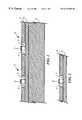
- the preferred semiconductor technology employed by the inventionis shown in FIG. 1 .
- the illustrated semiconductor materialincludes a silicon substrate 10 covered by an insulating layer 12 of silicon dioxide. Above the layer 12 is another layer 14 of silicon. It is in this layer 14 that transistors are formed for use in the distributed amplifier.
- MOSmetal oxide semiconductor
- NMOS transistor 16Two types are shown, an NMOS transistor 16 and a PMOS transistor 18 .
- the NMOS transistoris used in the distributed amplifier that is described later.
- the transistor 16is formed with an N region acting as a source (S), another N region acting as a drain (D), and a gate G.
- the transistor 18is formed by a pair of P regions acting as source and drain, and a gate G.
- a power output circuit according to the inventionmay also be implemented using a SOS (Silicon on Sapphire) process, as shown in FIG. 2 .
- SOSSilicon on Sapphire
- a sapphire substrate 19is covered by a silicon layer 20 .
- the transistor stages needed for coupling one transmission line to another transmission lineare formed in the layer 20 .
- One such transistoris shown, having a source (S), a drain (D) and a gate (G).
- distributed amplifier 21that is integrally constructed with the semiconductor material of FIG. 1 is shown in FIG. 3 .
- distributed amplifiermeans an amplifier having an input transmission line, an output transmission line, and multiple transistor stages that couple the transmission lines together by the transconductance of the transistor stages.
- the distributed amplifier 21has an input transmission line 22 that includes inductors 24 at the beginning and end of the transmission line 22 , and a series of inductors 26 connected between the inductors 24 ; the value of each inductor 24 is one-half the value of each inductor 26 .
- the input transmission lineis terminated by a resistance 28 of 50 ohms, with an RF bypass capacitor 30 coupled between the resistance 28 and ground.
- An output transmission line 32includes an inductor 34 at each end of the transmission line, and a series of inductances 36 connected between inductances 34 ; the value of inductors 34 is equal to the value of inductors 24 , and the value of inductors 36 is equal to the value of inductors 26 .
- a supply voltage for the distributed amplifieris provided by V+ which may be +1 volt.
- the V+ supplyis coupled to the transmission line 32 by an RF choke 35 .
- the termination for the output transmission lineis provided by a 50 ohm resistance 37 , with an RF bypass capacitor 31 coupled between the resistance 37 and ground.
- the input transmission line 22is coupled to the output transmission line 32 by the transconductance of N stages of transistors 38 .
- the gate of each transistoris coupled to a junction between adjacent inductors in the input transmission line 22 .
- the source of each transistoris grounded, with its drain coupled to a junction between adjacent inductors in the output transmission line 32 .
- a single transistor 38as a transistor stage, but other arrangements are also possible.
- a single transistor stagemay include two transistors coupled together as a cascode amplifier.
- Bias for the transistors 38is provided by a current source 39 coupled in series with the drain of a transistor 40 . With the drain of transistor 40 coupled to its gate, and the gate coupled to the input transmission line 22 through an isolating resistance 41 , equal bias currents are established in each of the transistors 38 . That bias current, 750 microamps in this example, is substantially equal to the current supplied by the current source 39 .
- each transistor 38becomes excited by the traveling signal and transfers the signal to the output transmission line through its transconductance.
- the signals output by the transistors 38are summed at an output terminal 44 . Any signal that propagates in the opposite direction is absorbed by the resistance 37 .
- a characteristic of distributed amplifiers that is used to advantage by this inventionis that the output power at terminal 44 is substantially equal to the sum of the individual power outputs of the transistors 38 .
- the number N of transistor stagesis selected to be equal to at least P d /Q.
- the distributed amplifier shown in FIG. 3was designed as the power output stage of a portable paging transmitter that is required to develop an output power P d of 320 mw (milliwatts). Assuming that each transistor 38 is capable of providing 20 mw, then 16 stages are required.
- the semiconductor area that is available for the distributed amplifiermay be large enough to allow an increase in the value of N, so that N exceeds the minimum value needed to provide the desired output power.
- the power associated with each stagecan be reduced. If the semiconductor material permits heat to be removed relatively fast, then each stage may be operated at its maximum permissible power, and the number of stages may be reduced. In any case, the stages should be physically separated from each other by a distance which permits the chip to dissipate heat without damage.
- the amplifier's frequency of operationis preferably between 16 and 32.
- the number of stages Nis preferably between 16 and 32.
- Sixteen stagesprovides a power output that is useful for many RF power applications, and spreads the power out among the individual stages so that it becomes practical to integrate the distributed amplifier on a chip with other components of an RF transceiver, thus making possible a “one-chip” transceiver.
- increasing the number of stages beyond 32brings into play the transistor's output resistances, as discussed above. For these reasons, it is preferred to select the number of stages, N, from the range 16 -32, inclusive.
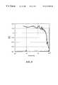
- a 16 stage distributed amplifieras shown in FIG. 3, was built using a 0.5 ⁇ (micron) SOI process.
- the transistorswere 25 ⁇ 0.5 ⁇ 20 fingers.
- the inductorsmay be formed conventionally, using the top metal layer of the SOI process to form metal strips.
- the inductors 26 and 36(FIG. 3) had a design value of 2 nanohenries, while inductors 24 and 34 had a design value of 1 nanohenry.
- the gain of the constructed amplifierwas 16 db at 12 ma drain current (750 ⁇ a per transistor) and a 1 volt V dd .
- the amplifierwas designed to be wafer probed, so as to reduce the effects of packaging on its performance.
- FIG. 4shows the performance of the constructed amplifier. Note the very useful gain out to about 3 gigahertz.
- FIG. 5an alternate embodiment of a power output circuit 48 according to the invention is shown. Certain obvious details, such as Vdd connections, have been omitted from FIG. 4 .
- This power output circuithas three transmission lines: a first or input transmission line 50 , having inductors 49 and 51 and an input 52 for receiving a signal to be amplified; a second transmission line 54 comprising inductors 49 and 51 ; and a third or output transmission line 56 having inductors 49 and 51 and an output 58 at which the output power is provided. All of the inductors 49 may be of equal value; and all of the inductors 51 may be of equal value, and preferably twice the value of inductors 49 .
- Stages of transistors 60are coupled as shown between the first transmission line 50 and the second transmission line 54 .
- Stages of transistors 62are coupled between the second transmission line 54 and the third transmission line 56 .
- Resistances 64 , 66 , 68 and 70provide proper terminations for the transmission lines to which they are coupled.
- the power output circuit 48acts as a distributed amplifier, as discussed previously in connection with FIG. 3 .
- the transconductances of transistor stages 60couple the first transmission line 50 to the second transmission line 54
- the transconductances of transistor stages 62couple the second transmission line 54 to the third transmission line 56 .
- the power developed by each of the transistor stages 60 , 62is summed at the output 58 .
- the power output circuit of FIG. 5may be expanded to include additional transmission lines situated between the input transmission line 50 and the output transmission line 56 .
- additional transmission linemay be added between the second transmission line 54 and the output transmission line 56 , with transistor stages coupling the additional transmission line to adjacent transmission lines, in the same manner as shown in FIG. 5 .
- the power output stages shown in FIGS. 3 and 5may also be implemented using the SOS process illustrated in FIG. 2 .
- a single IC chip 72includes conventional signal processing block 74 for amplifying, filtering and demodulating incoming signals, and a conventional frequency generation and modulation block 76 that includes the required oscillator(s), phase locked loop, and signal modulation circuitry.
- the modulated signal output from the block 76is applied to a conventional driver 78 which provides an amplified signal to a distributed amplifier 80 acting as a power output stage for driving a transmitting antenna (not shown).
- a controller 82 that controls various functions of the chip 72 in a conventional mannermay be a microprocessor, a state machine, or other form of logic circuit.
- the distributed amplifier 80may be of the type shown in FIGS. 3 or 4 , although the FIG. 3 embodiment is preferred, using 16 transistor stages and the component values described earlier for wideband operations up to about 1 gigahertz.
- the chip 72provides a power output of about 320 mw, which is suitable for many portable transceivers.
Landscapes
- Engineering & Computer Science (AREA)
- Power Engineering (AREA)
- Amplifiers (AREA)
Abstract
Description
Claims (27)
Priority Applications (1)
| Application Number | Priority Date | Filing Date | Title |
|---|---|---|---|
| US09/027,783US6215360B1 (en) | 1998-02-23 | 1998-02-23 | Semiconductor chip for RF transceiver and power output circuit therefor |
Applications Claiming Priority (1)
| Application Number | Priority Date | Filing Date | Title |
|---|---|---|---|
| US09/027,783US6215360B1 (en) | 1998-02-23 | 1998-02-23 | Semiconductor chip for RF transceiver and power output circuit therefor |
Publications (1)
| Publication Number | Publication Date |
|---|---|
| US6215360B1true US6215360B1 (en) | 2001-04-10 |
Family
ID=21839765
Family Applications (1)
| Application Number | Title | Priority Date | Filing Date |
|---|---|---|---|
| US09/027,783Expired - LifetimeUS6215360B1 (en) | 1998-02-23 | 1998-02-23 | Semiconductor chip for RF transceiver and power output circuit therefor |
Country Status (1)
| Country | Link |
|---|---|
| US (1) | US6215360B1 (en) |
Cited By (33)
| Publication number | Priority date | Publication date | Assignee | Title |
|---|---|---|---|---|
| US6531929B2 (en) | 1998-11-23 | 2003-03-11 | Micron Technology, Inc. | Monolithic integrated circuit oscillators, complementary metal oxide semiconductor (cmos) voltage-controlled oscillators, integrated circuit oscillators, oscillator-forming methods, and oscillation methods |
| US6593201B2 (en) | 1998-10-26 | 2003-07-15 | Micron Technology, Inc. | Monolithic inductance-enhancing integrated circuits, complementary metal oxide semiconductor (CMOS) inductance-enhancing integrated circuits, inductor assemblies, and inductance-multiplying methods |
| US6653691B2 (en) | 2000-11-16 | 2003-11-25 | Silicon Semiconductor Corporation | Radio frequency (RF) power devices having faraday shield layers therein |
| US20040027202A1 (en)* | 2002-01-25 | 2004-02-12 | Jerry Orr | Distributed level-shifting network for cascading broadband amplifiers |
| US20050248407A1 (en)* | 2004-04-29 | 2005-11-10 | Infineon Technologies Ag | Traveling wave amplifier |
| US20070207734A1 (en)* | 2006-02-17 | 2007-09-06 | International Rectifier Corporation | Wireless communication between control devices and controlled devices within a common board and rf high side coupler with plane polarized antenna |
| US7292828B1 (en)* | 2002-09-05 | 2007-11-06 | Case Western Reserve University | Miniaturized multichannel transmitter and wireless telemetry system |
| US20080076371A1 (en)* | 2005-07-11 | 2008-03-27 | Alexander Dribinsky | Circuit and method for controlling charge injection in radio frequency switches |
| US7420365B2 (en) | 2006-03-15 | 2008-09-02 | Honeywell International Inc. | Single chip MR sensor integrated with an RF transceiver |
| US7579913B1 (en) | 2008-02-27 | 2009-08-25 | United Microelectronics Corp. | Low power comsumption, low noise and high power gain distributed amplifiers for communication systems |
| US20110002080A1 (en)* | 2008-02-28 | 2011-01-06 | Peregrine Semiconductor Corporation | Method and apparatus for use in digitally tuning a capacitor in an integrated circuit device |
| US20110165759A1 (en)* | 2007-04-26 | 2011-07-07 | Robert Mark Englekirk | Tuning Capacitance to Enhance FET Stack Voltage Withstand |
| WO2012128686A1 (en)* | 2011-03-24 | 2012-09-27 | Saab Ab | A signal directing means for dividing an input signal into at least two output signals or combining at least two input signals into one output signal |
| US20120268213A1 (en)* | 2004-11-23 | 2012-10-25 | Bae Systems Information & Electronic Systems Integration Inc. | High power amplifier |
| US8405147B2 (en) | 2005-07-11 | 2013-03-26 | Peregrine Semiconductor Corporation | Method and apparatus for use in improving linearity of MOSFETs using an accumulated charge sink |
| US8559907B2 (en) | 2004-06-23 | 2013-10-15 | Peregrine Semiconductor Corporation | Integrated RF front end with stacked transistor switch |
| US8576009B2 (en) | 2004-11-23 | 2013-11-05 | Schilmass Co. L.L.C. | Broadband high power amplifier |
| US8583111B2 (en) | 2001-10-10 | 2013-11-12 | Peregrine Semiconductor Corporation | Switch circuit and method of switching radio frequency signals |
| US8723260B1 (en) | 2009-03-12 | 2014-05-13 | Rf Micro Devices, Inc. | Semiconductor radio frequency switch with body contact |
| US8742502B2 (en) | 2005-07-11 | 2014-06-03 | Peregrine Semiconductor Corporation | Method and apparatus for use in improving linearity of MOSFETs using an accumulated charge sink-harmonic wrinkle reduction |
| US8954902B2 (en) | 2005-07-11 | 2015-02-10 | Peregrine Semiconductor Corporation | Method and apparatus improving gate oxide reliability by controlling accumulated charge |
| US20160211694A1 (en)* | 2015-01-19 | 2016-07-21 | Anpec Electronics Corporation | Bidirectional wireless charging device and bidirectional wireless charging system |
| US9406695B2 (en) | 2013-11-20 | 2016-08-02 | Peregrine Semiconductor Corporation | Circuit and method for improving ESD tolerance and switching speed |
| US9419565B2 (en) | 2013-03-14 | 2016-08-16 | Peregrine Semiconductor Corporation | Hot carrier injection compensation |
| US9590674B2 (en) | 2012-12-14 | 2017-03-07 | Peregrine Semiconductor Corporation | Semiconductor devices with switchable ground-body connection |
| US9831857B2 (en) | 2015-03-11 | 2017-11-28 | Peregrine Semiconductor Corporation | Power splitter with programmable output phase shift |
| US9948281B2 (en) | 2016-09-02 | 2018-04-17 | Peregrine Semiconductor Corporation | Positive logic digitally tunable capacitor |
| US10236872B1 (en) | 2018-03-28 | 2019-03-19 | Psemi Corporation | AC coupling modules for bias ladders |
| US10505530B2 (en) | 2018-03-28 | 2019-12-10 | Psemi Corporation | Positive logic switch with selectable DC blocking circuit |
| US10886911B2 (en) | 2018-03-28 | 2021-01-05 | Psemi Corporation | Stacked FET switch bias ladders |
| US11011633B2 (en) | 2005-07-11 | 2021-05-18 | Psemi Corporation | Method and apparatus for use in improving linearity of MOSFETs using an accumulated charge sink-harmonic wrinkle reduction |
| USRE48965E1 (en) | 2005-07-11 | 2022-03-08 | Psemi Corporation | Method and apparatus improving gate oxide reliability by controlling accumulated charge |
| US11476849B2 (en) | 2020-01-06 | 2022-10-18 | Psemi Corporation | High power positive logic switch |
Citations (4)
| Publication number | Priority date | Publication date | Assignee | Title |
|---|---|---|---|---|
| US4418470A (en)* | 1981-10-21 | 1983-12-06 | General Electric Company | Method for fabricating silicon-on-sapphire monolithic microwave integrated circuits |
| US5021743A (en)* | 1989-11-30 | 1991-06-04 | Raytheon Company | Biasing networks for matrix amplifiers |
| US5663570A (en)* | 1993-07-12 | 1997-09-02 | Peregrine Semiconductor Corporation | High-frequency wireless communication system on a single ultrathin silicon on sapphire chip |
| US5939755A (en)* | 1995-06-08 | 1999-08-17 | Kabushiki Kaisha Toshiba | Power IC having high-side and low-side switches in an SOI structure |
- 1998
- 1998-02-23USUS09/027,783patent/US6215360B1/ennot_activeExpired - Lifetime
Patent Citations (4)
| Publication number | Priority date | Publication date | Assignee | Title |
|---|---|---|---|---|
| US4418470A (en)* | 1981-10-21 | 1983-12-06 | General Electric Company | Method for fabricating silicon-on-sapphire monolithic microwave integrated circuits |
| US5021743A (en)* | 1989-11-30 | 1991-06-04 | Raytheon Company | Biasing networks for matrix amplifiers |
| US5663570A (en)* | 1993-07-12 | 1997-09-02 | Peregrine Semiconductor Corporation | High-frequency wireless communication system on a single ultrathin silicon on sapphire chip |
| US5939755A (en)* | 1995-06-08 | 1999-08-17 | Kabushiki Kaisha Toshiba | Power IC having high-side and low-side switches in an SOI structure |
Non-Patent Citations (13)
| Title |
|---|
| "CMOS-Microwave Wideband Amplifiers and Mixers on SIMOX-Substrates", European solid-state circuits conference, Lille, France, Sep. 1995, pp. 302-305.* |
| "Distributed amplifiers: Their time comes again", part 1, Microwaves & RF, Nov. 1984 pp. 119-127* |
| "Distributed amplifiers: Their time comes again", part 2, Microwaves and RF, Dec. 1984, pp. 126-131 & 153.* |
| "MESFET Distributed Amplifier Design Guideline", James B. Beyer, S.N. Prasad, Robert C. Becker, James E. Nordman and Gert K. Hohenwarter IEEE Transaction on Microwave Theory and Techniques, bol. MTT-32, No. 3, Mar. 1984, pp. 268-275.* |
| "Silicon MOSFET distributed amplifier", Electronics Letters, Jun. 6, 1996, vol. 32 No. 12.* |
| Hitachi Releases Single-Chip High-Frequency Signal Processing IC for Digital Cellular Standards GSM-900, DCS-1800/1900 Dual-Bank Use, Hitachi 1999 http://global hitachi.com/New/cnews/E1999/991116B.html. |
| Huang, W. M., Ngo, D., Babcock, J., Shin, H.C., Welch, P., Rancanelli, M., Foerstner, J., Ford, J., and Cheng S., TFSOI Complementary BiCMOS Technology for Low Power RF mixed-Mode Applications, IEEE 1996, Advanced Custom Technologies, Motorola, Inc. 0-7803-3177-6. |
| Hughes, W. and Brucker G. J., Radiation Hardened MOS Technology, RCA Laboratories, NJ, Jul. 1979, Solid State Technology. |
| Power Amplifiers on Thin-FilmSilicon-on-Insulator (TFSOI) Technology by D. Ngo, W.M. Huang, J.M. Ford and Dan Spooner of Motorola Semiconductor Products Sector, Mesa, AZ, 1999 IEEE Internation SOI Conference, Oct. 1999, pp. 133-134. |
| Saul, P.H., The Bonded Wafer Silicon on Insulator Approach to High Performance Low Power Integrated Circuits, the Institution of Electricla Engineers, 1995, London UK. |
| Stanley, T. D., the State-of-the-Art in SOI Technology, Defense Nuclear Agency, Virginia USA 1999 IEEE 0018-9499/88/1200-1346301.00. |
| Tan, Y., Kumar, M., Sin, J., Shi, L., and Lau, J., "A 900-MHz Fully Integrated SOI Power Amplifier for Single-Chip Wireless Transceiver Applications," IEEE Journal of Solid-State Circuits, vol. 35, No. 10, Oct. 2000. |
| Thomas T. Y. Wong, Fundamentals of Distributed Amplification, Boston: Artech House 1993; ISBN 0-89006-615-9. |
Cited By (67)
| Publication number | Priority date | Publication date | Assignee | Title |
|---|---|---|---|---|
| US6593201B2 (en) | 1998-10-26 | 2003-07-15 | Micron Technology, Inc. | Monolithic inductance-enhancing integrated circuits, complementary metal oxide semiconductor (CMOS) inductance-enhancing integrated circuits, inductor assemblies, and inductance-multiplying methods |
| US6680518B2 (en)* | 1998-10-26 | 2004-01-20 | Micron Technology, Inc. | Monolithic inductance-enhancing integrated circuits, complementary metal oxide semiconductor (CMOS) inductance-enhancing integrated circuits, inductor assemblies, and inductance-multiplying methods |
| US6531929B2 (en) | 1998-11-23 | 2003-03-11 | Micron Technology, Inc. | Monolithic integrated circuit oscillators, complementary metal oxide semiconductor (cmos) voltage-controlled oscillators, integrated circuit oscillators, oscillator-forming methods, and oscillation methods |
| US6653691B2 (en) | 2000-11-16 | 2003-11-25 | Silicon Semiconductor Corporation | Radio frequency (RF) power devices having faraday shield layers therein |
| US10797694B2 (en) | 2001-10-10 | 2020-10-06 | Psemi Corporation | Switch circuit and method of switching radio frequency signals |
| US10812068B2 (en) | 2001-10-10 | 2020-10-20 | Psemi Corporation | Switch circuit and method of switching radio frequency signals |
| US9225378B2 (en) | 2001-10-10 | 2015-12-29 | Peregrine Semiconductor Corpopration | Switch circuit and method of switching radio frequency signals |
| US8583111B2 (en) | 2001-10-10 | 2013-11-12 | Peregrine Semiconductor Corporation | Switch circuit and method of switching radio frequency signals |
| US20040027202A1 (en)* | 2002-01-25 | 2004-02-12 | Jerry Orr | Distributed level-shifting network for cascading broadband amplifiers |
| US6759907B2 (en)* | 2002-01-25 | 2004-07-06 | Centellax, Inc. | Distributed level-shifting network for cascading broadband amplifiers |
| US7292828B1 (en)* | 2002-09-05 | 2007-11-06 | Case Western Reserve University | Miniaturized multichannel transmitter and wireless telemetry system |
| US7271657B2 (en)* | 2004-04-29 | 2007-09-18 | Infineon Technologies Ag | Traveling wave amplifier |
| US20050248407A1 (en)* | 2004-04-29 | 2005-11-10 | Infineon Technologies Ag | Traveling wave amplifier |
| US8559907B2 (en) | 2004-06-23 | 2013-10-15 | Peregrine Semiconductor Corporation | Integrated RF front end with stacked transistor switch |
| US9680416B2 (en) | 2004-06-23 | 2017-06-13 | Peregrine Semiconductor Corporation | Integrated RF front end with stacked transistor switch |
| US9369087B2 (en) | 2004-06-23 | 2016-06-14 | Peregrine Semiconductor Corporation | Integrated RF front end with stacked transistor switch |
| US8649754B2 (en) | 2004-06-23 | 2014-02-11 | Peregrine Semiconductor Corporation | Integrated RF front end with stacked transistor switch |
| US8576009B2 (en) | 2004-11-23 | 2013-11-05 | Schilmass Co. L.L.C. | Broadband high power amplifier |
| US20120268213A1 (en)* | 2004-11-23 | 2012-10-25 | Bae Systems Information & Electronic Systems Integration Inc. | High power amplifier |
| US8669812B2 (en)* | 2004-11-23 | 2014-03-11 | Schilmass Co., L.L.C. | High power amplifier |
| US8742502B2 (en) | 2005-07-11 | 2014-06-03 | Peregrine Semiconductor Corporation | Method and apparatus for use in improving linearity of MOSFETs using an accumulated charge sink-harmonic wrinkle reduction |
| US20080076371A1 (en)* | 2005-07-11 | 2008-03-27 | Alexander Dribinsky | Circuit and method for controlling charge injection in radio frequency switches |
| US9397656B2 (en) | 2005-07-11 | 2016-07-19 | Peregrine Semiconductor Corporation | Circuit and method for controlling charge injection in radio frequency switches |
| USRE48944E1 (en) | 2005-07-11 | 2022-02-22 | Psemi Corporation | Method and apparatus for use in improving linearity of MOSFETS using an accumulated charge sink |
| USRE48965E1 (en) | 2005-07-11 | 2022-03-08 | Psemi Corporation | Method and apparatus improving gate oxide reliability by controlling accumulated charge |
| US8405147B2 (en) | 2005-07-11 | 2013-03-26 | Peregrine Semiconductor Corporation | Method and apparatus for use in improving linearity of MOSFETs using an accumulated charge sink |
| US11011633B2 (en) | 2005-07-11 | 2021-05-18 | Psemi Corporation | Method and apparatus for use in improving linearity of MOSFETs using an accumulated charge sink-harmonic wrinkle reduction |
| US10797691B1 (en) | 2005-07-11 | 2020-10-06 | Psemi Corporation | Method and apparatus for use in improving linearity of MOSFETs using an accumulated charge sink |
| US12074217B2 (en) | 2005-07-11 | 2024-08-27 | Psemi Corporation | Method and apparatus for use in improving linearity of MOSFETs using an accumulated charge sink-harmonic wrinkle reduction |
| US8954902B2 (en) | 2005-07-11 | 2015-02-10 | Peregrine Semiconductor Corporation | Method and apparatus improving gate oxide reliability by controlling accumulated charge |
| US9608619B2 (en) | 2005-07-11 | 2017-03-28 | Peregrine Semiconductor Corporation | Method and apparatus improving gate oxide reliability by controlling accumulated charge |
| US9130564B2 (en) | 2005-07-11 | 2015-09-08 | Peregrine Semiconductor Corporation | Method and apparatus for use in improving linearity of MOSFETs using an accumulated charge sink |
| US9087899B2 (en) | 2005-07-11 | 2015-07-21 | Peregrine Semiconductor Corporation | Method and apparatus for use in improving linearity of MOSFETs using an accumulated charge sink-harmonic wrinkle reduction |
| US10804892B2 (en) | 2005-07-11 | 2020-10-13 | Psemi Corporation | Circuit and method for controlling charge injection in radio frequency switches |
| US20070207734A1 (en)* | 2006-02-17 | 2007-09-06 | International Rectifier Corporation | Wireless communication between control devices and controlled devices within a common board and rf high side coupler with plane polarized antenna |
| US7420365B2 (en) | 2006-03-15 | 2008-09-02 | Honeywell International Inc. | Single chip MR sensor integrated with an RF transceiver |
| US9177737B2 (en) | 2007-04-26 | 2015-11-03 | Peregrine Semiconductor Corporation | Tuning capacitance to enhance FET stack voltage withstand |
| US10951210B2 (en) | 2007-04-26 | 2021-03-16 | Psemi Corporation | Tuning capacitance to enhance FET stack voltage withstand |
| US8536636B2 (en) | 2007-04-26 | 2013-09-17 | Peregrine Semiconductor Corporation | Tuning capacitance to enhance FET stack voltage withstand |
| US20110165759A1 (en)* | 2007-04-26 | 2011-07-07 | Robert Mark Englekirk | Tuning Capacitance to Enhance FET Stack Voltage Withstand |
| US7579913B1 (en) | 2008-02-27 | 2009-08-25 | United Microelectronics Corp. | Low power comsumption, low noise and high power gain distributed amplifiers for communication systems |
| US20090212868A1 (en)* | 2008-02-27 | 2009-08-27 | United Microelectronics Corp. | Low power comsumption, low noise and high power gain distributed amplifers for communication systems |
| US9024700B2 (en) | 2008-02-28 | 2015-05-05 | Peregrine Semiconductor Corporation | Method and apparatus for use in digitally tuning a capacitor in an integrated circuit device |
| US9293262B2 (en) | 2008-02-28 | 2016-03-22 | Peregrine Semiconductor Corporation | Digitally tuned capacitors with tapered and reconfigurable quality factors |
| US20110002080A1 (en)* | 2008-02-28 | 2011-01-06 | Peregrine Semiconductor Corporation | Method and apparatus for use in digitally tuning a capacitor in an integrated circuit device |
| US8604864B2 (en) | 2008-02-28 | 2013-12-10 | Peregrine Semiconductor Corporation | Devices and methods for improving voltage handling and/or bi-directionality of stacks of elements when connected between terminals |
| US8669804B2 (en) | 2008-02-28 | 2014-03-11 | Peregrine Semiconductor Corporation | Devices and methods for improving voltage handling and/or bi-directionality of stacks of elements when connected between terminals |
| US9106227B2 (en) | 2008-02-28 | 2015-08-11 | Peregrine Semiconductor Corporation | Devices and methods for improving voltage handling and/or bi-directionality of stacks of elements when connected between terminals |
| US9197194B2 (en) | 2008-02-28 | 2015-11-24 | Peregrine Semiconductor Corporation | Methods and apparatuses for use in tuning reactance in a circuit device |
| US8723260B1 (en) | 2009-03-12 | 2014-05-13 | Rf Micro Devices, Inc. | Semiconductor radio frequency switch with body contact |
| US9024703B2 (en) | 2011-03-24 | 2015-05-05 | Saab Ab | Signal directing means for dividing an input signal into at least two output signals or combining at least two input signals into one output signal |
| WO2012128686A1 (en)* | 2011-03-24 | 2012-09-27 | Saab Ab | A signal directing means for dividing an input signal into at least two output signals or combining at least two input signals into one output signal |
| US9590674B2 (en) | 2012-12-14 | 2017-03-07 | Peregrine Semiconductor Corporation | Semiconductor devices with switchable ground-body connection |
| US9419565B2 (en) | 2013-03-14 | 2016-08-16 | Peregrine Semiconductor Corporation | Hot carrier injection compensation |
| US9406695B2 (en) | 2013-11-20 | 2016-08-02 | Peregrine Semiconductor Corporation | Circuit and method for improving ESD tolerance and switching speed |
| US20160211694A1 (en)* | 2015-01-19 | 2016-07-21 | Anpec Electronics Corporation | Bidirectional wireless charging device and bidirectional wireless charging system |
| US9876381B2 (en)* | 2015-01-19 | 2018-01-23 | Anpec Electronics Corporation | Bidirectional wireless charging device and bidirectional wireless charging system |
| US9831857B2 (en) | 2015-03-11 | 2017-11-28 | Peregrine Semiconductor Corporation | Power splitter with programmable output phase shift |
| US9948281B2 (en) | 2016-09-02 | 2018-04-17 | Peregrine Semiconductor Corporation | Positive logic digitally tunable capacitor |
| US10862473B2 (en) | 2018-03-28 | 2020-12-08 | Psemi Corporation | Positive logic switch with selectable DC blocking circuit |
| US10886911B2 (en) | 2018-03-28 | 2021-01-05 | Psemi Corporation | Stacked FET switch bias ladders |
| US10505530B2 (en) | 2018-03-28 | 2019-12-10 | Psemi Corporation | Positive logic switch with selectable DC blocking circuit |
| US11018662B2 (en) | 2018-03-28 | 2021-05-25 | Psemi Corporation | AC coupling modules for bias ladders |
| US11870431B2 (en) | 2018-03-28 | 2024-01-09 | Psemi Corporation | AC coupling modules for bias ladders |
| US10236872B1 (en) | 2018-03-28 | 2019-03-19 | Psemi Corporation | AC coupling modules for bias ladders |
| US11476849B2 (en) | 2020-01-06 | 2022-10-18 | Psemi Corporation | High power positive logic switch |
| US12081211B2 (en) | 2020-01-06 | 2024-09-03 | Psemi Corporation | High power positive logic switch |
Similar Documents
| Publication | Publication Date | Title |
|---|---|---|
| US6215360B1 (en) | Semiconductor chip for RF transceiver and power output circuit therefor | |
| US7109799B2 (en) | Current-controlled CMOS wideband data amplifier circuits | |
| US7995972B2 (en) | Electronic component for communication device and semiconductor device for switching transmission and reception | |
| US6748204B1 (en) | Mixer noise reduction technique | |
| JP6046004B2 (en) | CMOS transceiver with integrated power amplifier | |
| EP1451890B2 (en) | Switch circuit and method of switching radio frequency signals | |
| US7298600B2 (en) | Semiconductor integrated circuit device | |
| US20020079971A1 (en) | Compact cascode radio frequency CMOS power amplifier | |
| GB2331879A (en) | High frequency intergrated circuit for high-frequency radio transmitter-receiver suppressed in influence of high-frequency power leakage | |
| US20030184384A1 (en) | Voltage-limited distributed current source for ultra-broadband impedance termination | |
| CA2164995A1 (en) | Adiabatic mos oscillators | |
| US7187061B2 (en) | Use of a down-bond as a controlled inductor in integrated circuit applications | |
| US6469582B2 (en) | Voltage tunable active inductorless filter | |
| JPH01254013A (en) | Gallium arsenite monolithic microwave integrated circuit preamplifier | |
| JPH09121173A (en) | Semiconductor device containing power amplifier | |
| US5893027A (en) | Fully integrated two-way radio transmitter utilizing current mode transmit buffer and method of using same | |
| JP2894893B2 (en) | Mixer circuit | |
| US5705953A (en) | Device bias based supplemental amplification | |
| Kobayaski et al. | A monolithic HEMT-HBT direct-coupled amplifier with active input matching | |
| Kamogawa et al. | Wide-tuning range Si bipolar VCOs based on three-dimensional MMIC technology | |
| US8039880B2 (en) | High performance microwave switching devices and circuits |
Legal Events
| Date | Code | Title | Description |
|---|---|---|---|
| AS | Assignment | Owner name:MOTOROLA, INC., ILLINOIS Free format text:ASSIGNMENT OF ASSIGNORS INTEREST;ASSIGNOR:CALLAWAY, EDGAR HERBERT, JR.;REEL/FRAME:009017/0424 Effective date:19980217 | |
| STCF | Information on status: patent grant | Free format text:PATENTED CASE | |
| FPAY | Fee payment | Year of fee payment:4 | |
| FPAY | Fee payment | Year of fee payment:8 | |
| AS | Assignment | Owner name:MOTOROLA MOBILITY, INC, ILLINOIS Free format text:ASSIGNMENT OF ASSIGNORS INTEREST;ASSIGNOR:MOTOROLA, INC;REEL/FRAME:025673/0558 Effective date:20100731 | |
| FPAY | Fee payment | Year of fee payment:12 | |
| AS | Assignment | Owner name:MOTOROLA MOBILITY LLC, ILLINOIS Free format text:CHANGE OF NAME;ASSIGNOR:MOTOROLA MOBILITY, INC.;REEL/FRAME:029216/0282 Effective date:20120622 | |
| AS | Assignment | Owner name:GOOGLE TECHNOLOGY HOLDINGS LLC, CALIFORNIA Free format text:ASSIGNMENT OF ASSIGNORS INTEREST;ASSIGNOR:MOTOROLA MOBILITY LLC;REEL/FRAME:034489/0001 Effective date:20141028 |