US6215352B1 - Reference voltage generating circuit with MOS transistors having a floating gate - Google Patents
Reference voltage generating circuit with MOS transistors having a floating gateDownload PDFInfo
- Publication number
- US6215352B1 US6215352B1US09/236,331US23633199AUS6215352B1US 6215352 B1US6215352 B1US 6215352B1US 23633199 AUS23633199 AUS 23633199AUS 6215352 B1US6215352 B1US 6215352B1
- Authority
- US
- United States
- Prior art keywords
- mos transistor
- gate
- floating gate
- charge
- reference voltage
- Prior art date
- Legal status (The legal status is an assumption and is not a legal conclusion. Google has not performed a legal analysis and makes no representation as to the accuracy of the status listed.)
- Expired - Lifetime
Links
Images


Classifications
- G—PHYSICS
- G05—CONTROLLING; REGULATING
- G05F—SYSTEMS FOR REGULATING ELECTRIC OR MAGNETIC VARIABLES
- G05F3/00—Non-retroactive systems for regulating electric variables by using an uncontrolled element, or an uncontrolled combination of elements, such element or such combination having self-regulating properties
- G05F3/02—Regulating voltage or current
- G05F3/08—Regulating voltage or current wherein the variable is DC
- G05F3/10—Regulating voltage or current wherein the variable is DC using uncontrolled devices with non-linear characteristics
- G05F3/16—Regulating voltage or current wherein the variable is DC using uncontrolled devices with non-linear characteristics being semiconductor devices
- G05F3/20—Regulating voltage or current wherein the variable is DC using uncontrolled devices with non-linear characteristics being semiconductor devices using diode- transistor combinations
- G05F3/26—Current mirrors
- G—PHYSICS
- G05—CONTROLLING; REGULATING
- G05F—SYSTEMS FOR REGULATING ELECTRIC OR MAGNETIC VARIABLES
- G05F3/00—Non-retroactive systems for regulating electric variables by using an uncontrolled element, or an uncontrolled combination of elements, such element or such combination having self-regulating properties
- G05F3/02—Regulating voltage or current
- G05F3/08—Regulating voltage or current wherein the variable is DC
- G05F3/10—Regulating voltage or current wherein the variable is DC using uncontrolled devices with non-linear characteristics
- G05F3/16—Regulating voltage or current wherein the variable is DC using uncontrolled devices with non-linear characteristics being semiconductor devices
- G05F3/20—Regulating voltage or current wherein the variable is DC using uncontrolled devices with non-linear characteristics being semiconductor devices using diode- transistor combinations
- G05F3/24—Regulating voltage or current wherein the variable is DC using uncontrolled devices with non-linear characteristics being semiconductor devices using diode- transistor combinations wherein the transistors are of the field-effect type only
- G05F3/242—Regulating voltage or current wherein the variable is DC using uncontrolled devices with non-linear characteristics being semiconductor devices using diode- transistor combinations wherein the transistors are of the field-effect type only with compensation for device parameters, e.g. channel width modulation, threshold voltage, processing, or external variations, e.g. temperature, loading, supply voltage
Definitions
- the present inventionrelates to a reference voltage generating circuit mounted on a semiconductor integrated device for generating a reference voltage that exhibits little fluctuation caused by external variations.
- FIG. 1shows a circuit diagram of this type of reference voltage generating circuit of the prior art.
- This reference voltage generating circuitcomprises p-channel MOS transistors 11 - 13 , n-channel MOS transistors 21 - 24 , 45 , and 46 , and resistor 1 .
- P-channel MOS transistor 11has its source connected to power supply voltage VCC and its gate connected to reference voltage generating circuit activating signal BVREF.
- reference voltage generating circuit activating signal BVREFis low-level (hereinbelow abbreviated “L”) when activating the reference voltage generating circuit and high-level (hereinbelow abbreviated “H”) when deactivating the reference voltage generating circuit.
- Resistor 1is connected between the drain of p-channel MOS transistor 11 and the drain of n-channel MOS transistor 23 .
- N-channel MOS transistor 23has its gate and drain connected together, and has its source connected to ground.
- N-channel MOS transistor 21has its gate connected to the gate of n-channel MOS transistor 23 , thereby constituting together with n-channel MOS transistor 23 a current mirror circuit.
- P-channel MOS transistor 12has its gate and drain connected together, and has its source is connected to VCC, and has its drain connected to the drain of n-channel MOS transistor 21 .
- P-channel MOS transistor 13has its source connected to VCC, and its gate connected to the gate of p-channel MOS transistor 12 , thereby constituting together with p-channel MOS transistor 12 a current mirror circuit.
- N-channel MOS transistor 45has its drain connected to the drain of p-channel MOS transistor 13 , and its gate and drain connected together.
- N-channel MOS transistor 46has its drain connected to the drain of p-channel MOS transistor 13 , its gate and drain connected together, and its source connected to ground.
- N-channel MOS transistor 22has its drain connected to the source of n-channel MOS transistor 45 , its source connected to ground, and its gate connected to the gate of n-channel MOS transistor 23 .
- the gate width of n-channel MOS transistor 22is set to one-half that of n-channel MOS transistors 21 and 23 since that when the gate voltage is the same, one-half the current of n-channel MOS transistors 21 and 23 flows across the drain and source.
- the source voltage of n-channel MOS transistor 45is obtained as reference voltage VREF.
- N-channel MOS transistor 24has its gate which reference voltage generating circuit activating signal BVREF is applied to, its source grounded, and its drain connected to the gate of n-channel MOS transistor 23 .
- N-channel MOS transistor 24serves to render the gate voltage of n-channel MOS transistors 21 , 22 , 23 L when the operation of the reference voltage generating circuit is halted at the time reference voltage generating circuit activating signal BVREF has become H.
- reference voltage generating circuit activating signal BVREFis first rendered L to turn on p-channel MOS transistor 11 and turn off n-channel MOS transistor 24 .
- Current Iwhich is determined by resistor 1 and n-channel MOS transistor 23 , then flows across the drain and source of n-channel MOS transistor 23 to generate voltage V 1 , which is a voltage lower than power supply voltage VCC.
- the voltage V iis applied to the gate of n-channel MOS transistor 21 to cause current 21 to flow across the source and drain of n-channel MOS transistor 21 .
- voltage V 1is applied to its gate to cause current I, which is one-half the current of current 2 I, to flow across the source and drain.
- Current Ialso flows across the drain and source of n-channel MOS transistor 45 . Since provision is made for a current mirror circuit that allows current of the same level to flow to p-channel MOS transistor 12 and p-channel MOS transistor 13 , current 2 I will also flow across the source and drain of p-channel MOS transistor 13 .
- ⁇ 45 and ⁇ 46are the conductance coefficients of n-channel MOS transistors 45 and 46 , respectively, and V 2 is the drain voltage of p-channel MOS transistor 13 .
- a reference voltage generating circuit of the prior arthas the problem that only a particular fixed generated reference voltage VREF can be produced because the threshold values of n-channel MOS transistors 45 and 46 are fixed. Moreover, the reference voltage generating circuit of the aforementioned prior art also has the problem that variation in the characteristics of circuit elements at the time of fabrication results in variation in the obtained reference voltage, with the consequence that a reference voltage of a desired voltage cannot be obtained.
- the reference voltage generating circuitcomprises a first MOS transistor whose gate and drain are connected together, and a second MOS transistor whose gate and drain are connected together and which has a threshold value differing from the first MOS transistor.
- At least one MOS transistor of the first and second MOS transistorsis of a construction that includes a floating gate.
- the threshold voltage of the two MOS transistorscan therefore be set to any value, whereby the voltage value of the reference voltage can be set to any value.
- the reference voltage generating circuit of the inventionfurther includes means for controlling the amount of charge injected into the floating gate of a MOS transistor having a floating gate to alter the threshold voltage. This embodiment therefore allows the voltage value of the reference voltage to be freely reset after fabrication or after shipping.
- FIG. 1is a circuit diagram showing a reference voltage generating circuit of the prior art
- FIG. 2is a circuit diagram showing the reference voltage generating circuit according to a first embodiment of the present invention.
- FIG. 3is a circuit diagram showing the reference voltage generating circuit according to a second embodiment of the present invention.
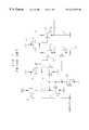
- the reference voltage generating circuitincludes n-channel MOS transistors 5 and 6 having floating gates in place of n-channel MOS transistors 45 and 46 in the reference voltage generating circuit of the prior art shown in FIG. 1, respectively.
- the threshold voltages of floating-gate n-channel MOS transistors 5 and 6are set to differing values, designated VT 5 and VT 6 , respectively.
- the voltage values VT 6 and VT 5 of the threshold voltagescan be freely set and the value of reference voltage VREF, which is the differential voltage of these voltage values can also be set to any value.
- This embodiment of the reference voltage generating circuitincludes n-channel MOS transistors 36 - 38 and voltage generating circuits 31 - 35 for setting the amount of charge injected to the floating gates of floating-gate n-channel MOS transistors 5 and 6 of the first embodiment of the reference voltage generating circuit shown in FIG. 2, and in addition, further includes a threshold value setting control circuit 26 .
- N-channel MOS transistor 38is connected between the drain of p-channel MOS transistor 13 and the drain of floating-gate n-channel MOS transistor 5 , and has its gate to which threshold value setting signal VTSET is applied.
- Threshold value setting signal VTSETbecomes L when setting the threshold voltages of floating-gate n-channel MOS transistors 5 and 6 , and becomes the VPP level when operating to generate reference voltage VREF.
- the VPP levelis a voltage level sufficient to turn on n-channel MOS transistors 36 , 37 , and 38 .
- N-channel MOS transistor 36is connected between the gate and drain of floating-gate n-channel MOS transistor 5
- n-channel MOS transistor 37is connected between the gate and drain of floating-gate n-channel MOS transistors 6
- threshold value setting signal VTSETis applied to the gate of each of n-channel MOS transistors 36 and 37 .
- n-channel MOS transistors 36 , 37 , and 38are turned off with the change of threshold value setting signal VTSET to L, whereby the gates and drains of floating gate n-channel MOS transistors 5 and 6 are disconnected, and p-channel MOS transistor 13 and floating-gate n-channel MOS transistor 5 are also disconnected.
- threshold value setting signal VTSETis changed to the VPP level to turn off (n-channel MOS transistors 36 , 37 , and 38 .
- operationis carried out equivalent to that of the reference voltage generating circuit shown in FIG. 2 .
- Threshold value setting control circuit 26comprises a write circuit 27 , an erase circuit 28 , and a read circuit 29 .
- Write circuit 27 , erase circuit 28 , and read circuit 29each effect control such that voltage generating circuits 31 - 35 output prescribed voltages during writing, erasing, and reading, respectively.
- Voltage generating circuit 31applies voltage to the drains of n-channel MOS transistors 5 and 6
- voltage generating circuit 32applies voltage to the gate of n-channel MOS transistor 5
- voltage generating circuit 33applies voltage to the gate of n-channel MOS transistor 6
- voltage generating circuit 34applies voltage to the source of n-channel MOS transistor 6
- voltage generating circuit 35applies voltage to the source of n-channel MOS transistor 5 .
- Voltage generating circuit 34produces the GND level potential during normal operation in which threshold value setting signal VTSET is of the VPP level, and applies the GND level potential to the source of floating gate n-channel MOS transistor 6 , thereby eliminating the need to connect the source of floating gate n-channel MOS transistor 6 to GND.
- Table 1 belowpresents an example of voltages produced in each of the modes by voltage generating circuits 31 - 35 under the control of write circuit 27 , erase circuit 28 , and read circuit 29 .
- Threshold value setting signal VTSETis first switched from VPP level to L level to place the reference voltage generating circuit in a threshold voltage setting state. Control is then effected by threshold value setting control circuit 26 as follows. To raise the threshold voltages of floating-gate n-channel MOS transistors 5 and 6 , voltages for writing are selected, 12 V being applied to each of the gates, 6 V being applied to each of the drains, and GND level being applied to each of the sources. Similarly, voltages for erasing are applied to each of the gates, drains, and sources of floating gate n-channel MOS transistors 5 and 6 to lower the threshold voltages. The threshold voltage of floating-gate n-channel MOS transistors 5 and 6 can thus be varied.
- the voltage values of 12 V and 6 Vare given herein by way of examples, and equivalent operation can be realized using other voltage values.
- the threshold voltages of both of floating-gate n-channel MOS transistors 5 and 6need not be changed at the same time, and a desired reference voltage VREF may be generated by changing only one of the voltages.
- threshold value setting signal VTSETis switched from the L to the VPP level to place the reference voltage generating circuit in a normal operation state.
- the reference voltage generating circuit according to this embodimenthas the same technical merit as the reference voltage generating circuit according to the first embodiment described hereinabove, and in addition, enables resetting of the voltage value of reference voltage VREF produced because the threshold voltages of floating-gate n-channel MOS transistors 5 and 6 can be altered.
- the circuit configurationmay take any form as long as at least one of the two MOS transistors is a transistor having a floating gate.
- the present inventioncan be realized even if the power supply voltage and ground are switched and the conductivity is reversed in the circuit configurations of the first and second embodiments.
- the threshold value setting method described in the second embodimentmay take another form such as irradiation by ultraviolet light.
Landscapes
- Engineering & Computer Science (AREA)
- Physics & Mathematics (AREA)
- Microelectronics & Electronic Packaging (AREA)
- Nonlinear Science (AREA)
- Electromagnetism (AREA)
- General Physics & Mathematics (AREA)
- Radar, Positioning & Navigation (AREA)
- Automation & Control Theory (AREA)
- Control Of Electrical Variables (AREA)
- Static Random-Access Memory (AREA)
- Read Only Memory (AREA)
- Semiconductor Integrated Circuits (AREA)
Abstract
Description
| TABLE 1 | |||||
| Drain | Gate | Source | |||
| Voltage | Voltage | Voltage | |||
| generating circuit | generating | generating | |||
| 31 | |||||
| Write | 6 V | 12 V | GND | ||
| Erase | Open | GND | 12 V | ||
| Read | VCC | 6 V | GND | ||
Claims (18)
Applications Claiming Priority (2)
| Application Number | Priority Date | Filing Date | Title |
|---|---|---|---|
| JP1566798AJP3139542B2 (en) | 1998-01-28 | 1998-01-28 | Reference voltage generation circuit |
| JP10-015667 | 1998-01-28 |
Publications (1)
| Publication Number | Publication Date |
|---|---|
| US6215352B1true US6215352B1 (en) | 2001-04-10 |
Family
ID=11895103
Family Applications (1)
| Application Number | Title | Priority Date | Filing Date |
|---|---|---|---|
| US09/236,331Expired - LifetimeUS6215352B1 (en) | 1998-01-28 | 1999-01-25 | Reference voltage generating circuit with MOS transistors having a floating gate |
Country Status (4)
| Country | Link |
|---|---|
| US (1) | US6215352B1 (en) |
| JP (1) | JP3139542B2 (en) |
| KR (1) | KR100326824B1 (en) |
| CN (1) | CN1169155C (en) |
Cited By (46)
| Publication number | Priority date | Publication date | Assignee | Title |
|---|---|---|---|---|
| US20030146785A1 (en)* | 2000-06-23 | 2003-08-07 | Yoshinori Ueda | Voltage reference generation circuit and power source incorporating such circuit |
| US6768371B1 (en) | 2003-03-20 | 2004-07-27 | Ami Semiconductor, Inc. | Stable floating gate voltage reference using interconnected current-to-voltage and voltage-to-current converters |
| US20080136470A1 (en)* | 2004-03-25 | 2008-06-12 | Nathan Moyal | Method and circuit for rapid alignment of signals |
| US20080258759A1 (en)* | 2007-04-17 | 2008-10-23 | Cypress Semiconductor Corporation | Universal digital block interconnection and channel routing |
| US20080259702A1 (en)* | 2007-04-17 | 2008-10-23 | Cypress Semiconductor Corporation | State-monitoring memory element |
| US20080297388A1 (en)* | 2007-04-17 | 2008-12-04 | Cypress Semiconductor Corporation | Programmable sigma-delta analog-to-digital converter |
| US20080312857A1 (en)* | 2006-03-27 | 2008-12-18 | Seguine Dennis R | Input/output multiplexer bus |
| US20090015320A1 (en)* | 2004-01-05 | 2009-01-15 | Intersil Americas Inc. | Temperature compensation for floating gate circuits |
| US20090066427A1 (en)* | 2005-02-04 | 2009-03-12 | Aaron Brennan | Poly-phase frequency synthesis oscillator |
| US20090146731A1 (en)* | 2006-03-31 | 2009-06-11 | Ricoh Company, Ltd | Reference voltage generating circuit and power supply device using the same |
| US20090146499A1 (en)* | 2007-12-06 | 2009-06-11 | Seiko Instruments Inc. | Power supply switching circuit |
| US7761845B1 (en) | 2002-09-09 | 2010-07-20 | Cypress Semiconductor Corporation | Method for parameterizing a user module |
| US7765095B1 (en) | 2000-10-26 | 2010-07-27 | Cypress Semiconductor Corporation | Conditional branching in an in-circuit emulation system |
| US7770113B1 (en) | 2001-11-19 | 2010-08-03 | Cypress Semiconductor Corporation | System and method for dynamically generating a configuration datasheet |
| US7774190B1 (en) | 2001-11-19 | 2010-08-10 | Cypress Semiconductor Corporation | Sleep and stall in an in-circuit emulation system |
| US7825688B1 (en) | 2000-10-26 | 2010-11-02 | Cypress Semiconductor Corporation | Programmable microcontroller architecture(mixed analog/digital) |
| US7844437B1 (en) | 2001-11-19 | 2010-11-30 | Cypress Semiconductor Corporation | System and method for performing next placements and pruning of disallowed placements for programming an integrated circuit |
| US20110187447A1 (en)* | 2010-02-04 | 2011-08-04 | Iacob Radu H | Mixed-mode circuits and methods of producing a reference current and a reference voltage |
| US20110187344A1 (en)* | 2010-02-04 | 2011-08-04 | Iacob Radu H | Current-mode programmable reference circuits and methods therefor |
| US20110193544A1 (en)* | 2010-02-11 | 2011-08-11 | Iacob Radu H | Circuits and methods of producing a reference current or voltage |
| US8026739B2 (en) | 2007-04-17 | 2011-09-27 | Cypress Semiconductor Corporation | System level interconnect with programmable switching |
| US8049569B1 (en) | 2007-09-05 | 2011-11-01 | Cypress Semiconductor Corporation | Circuit and method for improving the accuracy of a crystal-less oscillator having dual-frequency modes |
| US8069428B1 (en) | 2001-10-24 | 2011-11-29 | Cypress Semiconductor Corporation | Techniques for generating microcontroller configuration information |
| US8069405B1 (en) | 2001-11-19 | 2011-11-29 | Cypress Semiconductor Corporation | User interface for efficiently browsing an electronic document using data-driven tabs |
| US8078970B1 (en) | 2001-11-09 | 2011-12-13 | Cypress Semiconductor Corporation | Graphical user interface with user-selectable list-box |
| US8078894B1 (en) | 2007-04-25 | 2011-12-13 | Cypress Semiconductor Corporation | Power management architecture, method and configuration system |
| US8085067B1 (en) | 2005-12-21 | 2011-12-27 | Cypress Semiconductor Corporation | Differential-to-single ended signal converter circuit and method |
| US8089461B2 (en) | 2005-06-23 | 2012-01-03 | Cypress Semiconductor Corporation | Touch wake for electronic devices |
| US8092083B2 (en) | 2007-04-17 | 2012-01-10 | Cypress Semiconductor Corporation | Temperature sensor with digital bandgap |
| US8103497B1 (en) | 2002-03-28 | 2012-01-24 | Cypress Semiconductor Corporation | External interface for event architecture |
| US8103496B1 (en) | 2000-10-26 | 2012-01-24 | Cypress Semicondutor Corporation | Breakpoint control in an in-circuit emulation system |
| US8120408B1 (en) | 2005-05-05 | 2012-02-21 | Cypress Semiconductor Corporation | Voltage controlled oscillator delay cell and method |
| US8130025B2 (en) | 2007-04-17 | 2012-03-06 | Cypress Semiconductor Corporation | Numerical band gap |
| US8149048B1 (en) | 2000-10-26 | 2012-04-03 | Cypress Semiconductor Corporation | Apparatus and method for programmable power management in a programmable analog circuit block |
| US8160864B1 (en) | 2000-10-26 | 2012-04-17 | Cypress Semiconductor Corporation | In-circuit emulator and pod synchronized boot |
| US8176296B2 (en) | 2000-10-26 | 2012-05-08 | Cypress Semiconductor Corporation | Programmable microcontroller architecture |
| US8402313B1 (en) | 2002-05-01 | 2013-03-19 | Cypress Semiconductor Corporation | Reconfigurable testing system and method |
| US8499270B1 (en) | 2007-04-25 | 2013-07-30 | Cypress Semiconductor Corporation | Configuration of programmable IC design elements |
| US8516025B2 (en) | 2007-04-17 | 2013-08-20 | Cypress Semiconductor Corporation | Clock driven dynamic datapath chaining |
| US8527949B1 (en) | 2001-11-19 | 2013-09-03 | Cypress Semiconductor Corporation | Graphical user interface for dynamically reconfiguring a programmable device |
| US9448964B2 (en) | 2009-05-04 | 2016-09-20 | Cypress Semiconductor Corporation | Autonomous control in a programmable system |
| US20160342185A1 (en)* | 2015-05-22 | 2016-11-24 | Advanced Micro Devices, Inc. | Droop detection and regulation for processor tiles |
| US9564902B2 (en) | 2007-04-17 | 2017-02-07 | Cypress Semiconductor Corporation | Dynamically configurable and re-configurable data path |
| US9720805B1 (en) | 2007-04-25 | 2017-08-01 | Cypress Semiconductor Corporation | System and method for controlling a target device |
| US10698662B2 (en) | 2001-11-15 | 2020-06-30 | Cypress Semiconductor Corporation | System providing automatic source code generation for personalization and parameterization of user modules |
| US10782723B1 (en) | 2019-11-01 | 2020-09-22 | Analog Devices International Unlimited Company | Reference generator using fet devices with different gate work functions |
Families Citing this family (5)
| Publication number | Priority date | Publication date | Assignee | Title |
|---|---|---|---|---|
| US6870764B2 (en)* | 2003-01-21 | 2005-03-22 | Xicor Corporation | Floating gate analog voltage feedback circuit |
| US9411348B2 (en)* | 2010-04-13 | 2016-08-09 | Semiconductor Components Industries, Llc | Programmable low-dropout regulator and methods therefor |
| CN101814829B (en)* | 2010-04-22 | 2015-09-16 | 上海华虹宏力半导体制造有限公司 | The generating circuit from reference voltage of charge pump circuit and charge pump circuit |
| CN103886903B (en)* | 2012-12-21 | 2017-11-03 | 华邦电子股份有限公司 | Reference cell scheme and method to produce reference current |
| KR102583770B1 (en)* | 2016-09-12 | 2023-10-06 | 삼성디스플레이 주식회사 | Memory transistor and display apparatus having the same |
Citations (14)
| Publication number | Priority date | Publication date | Assignee | Title |
|---|---|---|---|---|
| JPS59212927A (en) | 1983-05-18 | 1984-12-01 | Mitsubishi Electric Corp | Constant voltage generating circuit |
| JPS601018A (en) | 1983-06-20 | 1985-01-07 | Mitsubishi Electric Corp | Car air conditioner |
| US4498040A (en)* | 1977-04-26 | 1985-02-05 | Kabushiki Kaisha Suwa Seikosha | Reference voltage circuit |
| JPS6121515A (en) | 1984-09-28 | 1986-01-30 | Hitachi Ltd | Semiconductor integrated circuit device |
| JPH01296491A (en) | 1988-05-25 | 1989-11-29 | Hitachi Ltd | Reference voltage generation circuit |
| JPH0290307A (en) | 1988-09-28 | 1990-03-29 | Nec Corp | Programmable reference voltage generator |
| JPH02245810A (en) | 1989-03-20 | 1990-10-01 | Hitachi Ltd | Reference voltage generation circuit |
| JPH02245913A (en) | 1989-03-20 | 1990-10-01 | Mitsubishi Electric Corp | Constant voltage generating circuit |
| JPH05119859A (en) | 1991-10-24 | 1993-05-18 | Sony Corp | Reference voltage generating circuit |
| US5218571A (en)* | 1990-05-07 | 1993-06-08 | Cypress Semiconductor Corporation | EPROM source bias circuit with compensation for processing characteristics |
| JPH0750563A (en) | 1993-04-02 | 1995-02-21 | Gemplus Card Internatl Sa | Automatic trigger circuit |
| JPH08211953A (en) | 1995-01-31 | 1996-08-20 | Nkk Corp | Semiconductor regulator device |
| JPH097380A (en) | 1995-06-20 | 1997-01-10 | Nec Corp | Nonvolatile semiconductor memory device |
| US5629893A (en)* | 1995-05-12 | 1997-05-13 | Advanced Micro Devices, Inc. | System for constant field erasure in a flash EPROM |
- 1998
- 1998-01-28JPJP1566798Apatent/JP3139542B2/ennot_activeExpired - Fee Related
- 1999
- 1999-01-22KRKR1019990001875Apatent/KR100326824B1/ennot_activeExpired - Fee Related
- 1999-01-25USUS09/236,331patent/US6215352B1/ennot_activeExpired - Lifetime
- 1999-01-28CNCNB991017099Apatent/CN1169155C/ennot_activeExpired - Fee Related
Patent Citations (14)
| Publication number | Priority date | Publication date | Assignee | Title |
|---|---|---|---|---|
| US4498040A (en)* | 1977-04-26 | 1985-02-05 | Kabushiki Kaisha Suwa Seikosha | Reference voltage circuit |
| JPS59212927A (en) | 1983-05-18 | 1984-12-01 | Mitsubishi Electric Corp | Constant voltage generating circuit |
| JPS601018A (en) | 1983-06-20 | 1985-01-07 | Mitsubishi Electric Corp | Car air conditioner |
| JPS6121515A (en) | 1984-09-28 | 1986-01-30 | Hitachi Ltd | Semiconductor integrated circuit device |
| JPH01296491A (en) | 1988-05-25 | 1989-11-29 | Hitachi Ltd | Reference voltage generation circuit |
| JPH0290307A (en) | 1988-09-28 | 1990-03-29 | Nec Corp | Programmable reference voltage generator |
| JPH02245810A (en) | 1989-03-20 | 1990-10-01 | Hitachi Ltd | Reference voltage generation circuit |
| JPH02245913A (en) | 1989-03-20 | 1990-10-01 | Mitsubishi Electric Corp | Constant voltage generating circuit |
| US5218571A (en)* | 1990-05-07 | 1993-06-08 | Cypress Semiconductor Corporation | EPROM source bias circuit with compensation for processing characteristics |
| JPH05119859A (en) | 1991-10-24 | 1993-05-18 | Sony Corp | Reference voltage generating circuit |
| JPH0750563A (en) | 1993-04-02 | 1995-02-21 | Gemplus Card Internatl Sa | Automatic trigger circuit |
| JPH08211953A (en) | 1995-01-31 | 1996-08-20 | Nkk Corp | Semiconductor regulator device |
| US5629893A (en)* | 1995-05-12 | 1997-05-13 | Advanced Micro Devices, Inc. | System for constant field erasure in a flash EPROM |
| JPH097380A (en) | 1995-06-20 | 1997-01-10 | Nec Corp | Nonvolatile semiconductor memory device |
Cited By (80)
| Publication number | Priority date | Publication date | Assignee | Title |
|---|---|---|---|---|
| US6798278B2 (en)* | 2000-06-23 | 2004-09-28 | Ricoh Company, Ltd. | Voltage reference generation circuit and power source incorporating such circuit |
| US20030146785A1 (en)* | 2000-06-23 | 2003-08-07 | Yoshinori Ueda | Voltage reference generation circuit and power source incorporating such circuit |
| US7765095B1 (en) | 2000-10-26 | 2010-07-27 | Cypress Semiconductor Corporation | Conditional branching in an in-circuit emulation system |
| US8555032B2 (en) | 2000-10-26 | 2013-10-08 | Cypress Semiconductor Corporation | Microcontroller programmable system on a chip with programmable interconnect |
| US8160864B1 (en) | 2000-10-26 | 2012-04-17 | Cypress Semiconductor Corporation | In-circuit emulator and pod synchronized boot |
| US8176296B2 (en) | 2000-10-26 | 2012-05-08 | Cypress Semiconductor Corporation | Programmable microcontroller architecture |
| US8358150B1 (en) | 2000-10-26 | 2013-01-22 | Cypress Semiconductor Corporation | Programmable microcontroller architecture(mixed analog/digital) |
| US10248604B2 (en) | 2000-10-26 | 2019-04-02 | Cypress Semiconductor Corporation | Microcontroller programmable system on a chip |
| US8149048B1 (en) | 2000-10-26 | 2012-04-03 | Cypress Semiconductor Corporation | Apparatus and method for programmable power management in a programmable analog circuit block |
| US10020810B2 (en) | 2000-10-26 | 2018-07-10 | Cypress Semiconductor Corporation | PSoC architecture |
| US9843327B1 (en) | 2000-10-26 | 2017-12-12 | Cypress Semiconductor Corporation | PSOC architecture |
| US9766650B2 (en) | 2000-10-26 | 2017-09-19 | Cypress Semiconductor Corporation | Microcontroller programmable system on a chip with programmable interconnect |
| US8103496B1 (en) | 2000-10-26 | 2012-01-24 | Cypress Semicondutor Corporation | Breakpoint control in an in-circuit emulation system |
| US8736303B2 (en) | 2000-10-26 | 2014-05-27 | Cypress Semiconductor Corporation | PSOC architecture |
| US10725954B2 (en) | 2000-10-26 | 2020-07-28 | Monterey Research, Llc | Microcontroller programmable system on a chip |
| US7825688B1 (en) | 2000-10-26 | 2010-11-02 | Cypress Semiconductor Corporation | Programmable microcontroller architecture(mixed analog/digital) |
| US10261932B2 (en) | 2000-10-26 | 2019-04-16 | Cypress Semiconductor Corporation | Microcontroller programmable system on a chip |
| US8069428B1 (en) | 2001-10-24 | 2011-11-29 | Cypress Semiconductor Corporation | Techniques for generating microcontroller configuration information |
| US10466980B2 (en) | 2001-10-24 | 2019-11-05 | Cypress Semiconductor Corporation | Techniques for generating microcontroller configuration information |
| US8793635B1 (en) | 2001-10-24 | 2014-07-29 | Cypress Semiconductor Corporation | Techniques for generating microcontroller configuration information |
| US8078970B1 (en) | 2001-11-09 | 2011-12-13 | Cypress Semiconductor Corporation | Graphical user interface with user-selectable list-box |
| US10698662B2 (en) | 2001-11-15 | 2020-06-30 | Cypress Semiconductor Corporation | System providing automatic source code generation for personalization and parameterization of user modules |
| US8533677B1 (en) | 2001-11-19 | 2013-09-10 | Cypress Semiconductor Corporation | Graphical user interface for dynamically reconfiguring a programmable device |
| US8370791B2 (en) | 2001-11-19 | 2013-02-05 | Cypress Semiconductor Corporation | System and method for performing next placements and pruning of disallowed placements for programming an integrated circuit |
| US7770113B1 (en) | 2001-11-19 | 2010-08-03 | Cypress Semiconductor Corporation | System and method for dynamically generating a configuration datasheet |
| US7774190B1 (en) | 2001-11-19 | 2010-08-10 | Cypress Semiconductor Corporation | Sleep and stall in an in-circuit emulation system |
| US7844437B1 (en) | 2001-11-19 | 2010-11-30 | Cypress Semiconductor Corporation | System and method for performing next placements and pruning of disallowed placements for programming an integrated circuit |
| US8527949B1 (en) | 2001-11-19 | 2013-09-03 | Cypress Semiconductor Corporation | Graphical user interface for dynamically reconfiguring a programmable device |
| US8069405B1 (en) | 2001-11-19 | 2011-11-29 | Cypress Semiconductor Corporation | User interface for efficiently browsing an electronic document using data-driven tabs |
| US8103497B1 (en) | 2002-03-28 | 2012-01-24 | Cypress Semiconductor Corporation | External interface for event architecture |
| US8402313B1 (en) | 2002-05-01 | 2013-03-19 | Cypress Semiconductor Corporation | Reconfigurable testing system and method |
| US7761845B1 (en) | 2002-09-09 | 2010-07-20 | Cypress Semiconductor Corporation | Method for parameterizing a user module |
| US6768371B1 (en) | 2003-03-20 | 2004-07-27 | Ami Semiconductor, Inc. | Stable floating gate voltage reference using interconnected current-to-voltage and voltage-to-current converters |
| US20090015320A1 (en)* | 2004-01-05 | 2009-01-15 | Intersil Americas Inc. | Temperature compensation for floating gate circuits |
| US7893724B2 (en) | 2004-03-25 | 2011-02-22 | Cypress Semiconductor Corporation | Method and circuit for rapid alignment of signals |
| US20080136470A1 (en)* | 2004-03-25 | 2008-06-12 | Nathan Moyal | Method and circuit for rapid alignment of signals |
| US20090066427A1 (en)* | 2005-02-04 | 2009-03-12 | Aaron Brennan | Poly-phase frequency synthesis oscillator |
| US8085100B2 (en) | 2005-02-04 | 2011-12-27 | Cypress Semiconductor Corporation | Poly-phase frequency synthesis oscillator |
| US8120408B1 (en) | 2005-05-05 | 2012-02-21 | Cypress Semiconductor Corporation | Voltage controlled oscillator delay cell and method |
| US8089461B2 (en) | 2005-06-23 | 2012-01-03 | Cypress Semiconductor Corporation | Touch wake for electronic devices |
| US8085067B1 (en) | 2005-12-21 | 2011-12-27 | Cypress Semiconductor Corporation | Differential-to-single ended signal converter circuit and method |
| US8717042B1 (en) | 2006-03-27 | 2014-05-06 | Cypress Semiconductor Corporation | Input/output multiplexer bus |
| US8067948B2 (en) | 2006-03-27 | 2011-11-29 | Cypress Semiconductor Corporation | Input/output multiplexer bus |
| US20080312857A1 (en)* | 2006-03-27 | 2008-12-18 | Seguine Dennis R | Input/output multiplexer bus |
| US20090146731A1 (en)* | 2006-03-31 | 2009-06-11 | Ricoh Company, Ltd | Reference voltage generating circuit and power supply device using the same |
| US7982531B2 (en)* | 2006-03-31 | 2011-07-19 | Ricoh Company, Ltd. | Reference voltage generating circuit and power supply device using the same |
| US8462576B2 (en) | 2007-04-17 | 2013-06-11 | Cypress Semiconductor Corporation | State-monitoring memory element |
| US8516025B2 (en) | 2007-04-17 | 2013-08-20 | Cypress Semiconductor Corporation | Clock driven dynamic datapath chaining |
| US8130025B2 (en) | 2007-04-17 | 2012-03-06 | Cypress Semiconductor Corporation | Numerical band gap |
| US20080258759A1 (en)* | 2007-04-17 | 2008-10-23 | Cypress Semiconductor Corporation | Universal digital block interconnection and channel routing |
| US7737724B2 (en) | 2007-04-17 | 2010-06-15 | Cypress Semiconductor Corporation | Universal digital block interconnection and channel routing |
| US8476928B1 (en) | 2007-04-17 | 2013-07-02 | Cypress Semiconductor Corporation | System level interconnect with programmable switching |
| US8111577B2 (en)* | 2007-04-17 | 2012-02-07 | Cypress Semiconductor Corporation | System comprising a state-monitoring memory element |
| US8026739B2 (en) | 2007-04-17 | 2011-09-27 | Cypress Semiconductor Corporation | System level interconnect with programmable switching |
| US20080259702A1 (en)* | 2007-04-17 | 2008-10-23 | Cypress Semiconductor Corporation | State-monitoring memory element |
| US20080297388A1 (en)* | 2007-04-17 | 2008-12-04 | Cypress Semiconductor Corporation | Programmable sigma-delta analog-to-digital converter |
| US8040266B2 (en) | 2007-04-17 | 2011-10-18 | Cypress Semiconductor Corporation | Programmable sigma-delta analog-to-digital converter |
| US9564902B2 (en) | 2007-04-17 | 2017-02-07 | Cypress Semiconductor Corporation | Dynamically configurable and re-configurable data path |
| US8705309B2 (en) | 2007-04-17 | 2014-04-22 | Cypress Semiconductor Corporation | State-monitoring memory element |
| US8092083B2 (en) | 2007-04-17 | 2012-01-10 | Cypress Semiconductor Corporation | Temperature sensor with digital bandgap |
| US8078894B1 (en) | 2007-04-25 | 2011-12-13 | Cypress Semiconductor Corporation | Power management architecture, method and configuration system |
| US9720805B1 (en) | 2007-04-25 | 2017-08-01 | Cypress Semiconductor Corporation | System and method for controlling a target device |
| US8499270B1 (en) | 2007-04-25 | 2013-07-30 | Cypress Semiconductor Corporation | Configuration of programmable IC design elements |
| US8909960B1 (en) | 2007-04-25 | 2014-12-09 | Cypress Semiconductor Corporation | Power management architecture, method and configuration system |
| US8049569B1 (en) | 2007-09-05 | 2011-11-01 | Cypress Semiconductor Corporation | Circuit and method for improving the accuracy of a crystal-less oscillator having dual-frequency modes |
| US7826297B2 (en)* | 2007-12-06 | 2010-11-02 | Seiko Instruments Inc. | Power supply switching circuit |
| US20090146499A1 (en)* | 2007-12-06 | 2009-06-11 | Seiko Instruments Inc. | Power supply switching circuit |
| US9448964B2 (en) | 2009-05-04 | 2016-09-20 | Cypress Semiconductor Corporation | Autonomous control in a programmable system |
| US8188785B2 (en) | 2010-02-04 | 2012-05-29 | Semiconductor Components Industries, Llc | Mixed-mode circuits and methods of producing a reference current and a reference voltage |
| US8878511B2 (en)* | 2010-02-04 | 2014-11-04 | Semiconductor Components Industries, Llc | Current-mode programmable reference circuits and methods therefor |
| US20110187447A1 (en)* | 2010-02-04 | 2011-08-04 | Iacob Radu H | Mixed-mode circuits and methods of producing a reference current and a reference voltage |
| US20110187344A1 (en)* | 2010-02-04 | 2011-08-04 | Iacob Radu H | Current-mode programmable reference circuits and methods therefor |
| CN102156506B (en)* | 2010-02-11 | 2014-09-24 | 半导体元件工业有限责任公司 | Circuits and methods of producing a reference current or voltage |
| US8680840B2 (en)* | 2010-02-11 | 2014-03-25 | Semiconductor Components Industries, Llc | Circuits and methods of producing a reference current or voltage |
| US20110193544A1 (en)* | 2010-02-11 | 2011-08-11 | Iacob Radu H | Circuits and methods of producing a reference current or voltage |
| CN102156506A (en)* | 2010-02-11 | 2011-08-17 | 半导体元件工业有限责任公司 | Circuits and methods of producing a reference current or voltage |
| US20160342185A1 (en)* | 2015-05-22 | 2016-11-24 | Advanced Micro Devices, Inc. | Droop detection and regulation for processor tiles |
| US10248177B2 (en)* | 2015-05-22 | 2019-04-02 | Advanced Micro Devices, Inc. | Droop detection and regulation for processor tiles |
| US10782723B1 (en) | 2019-11-01 | 2020-09-22 | Analog Devices International Unlimited Company | Reference generator using fet devices with different gate work functions |
| US11687111B2 (en) | 2019-11-01 | 2023-06-27 | Analog Devices International Unlimited Company | Reference generator using FET devices with different gate work functions |
Also Published As
| Publication number | Publication date |
|---|---|
| CN1228597A (en) | 1999-09-15 |
| JPH11212660A (en) | 1999-08-06 |
| KR100326824B1 (en) | 2002-03-04 |
| CN1169155C (en) | 2004-09-29 |
| KR19990068062A (en) | 1999-08-25 |
| JP3139542B2 (en) | 2001-03-05 |
Similar Documents
| Publication | Publication Date | Title |
|---|---|---|
| US6215352B1 (en) | Reference voltage generating circuit with MOS transistors having a floating gate | |
| US4727309A (en) | Current difference current source | |
| US6535423B2 (en) | Drain bias for non-volatile memory | |
| US5706240A (en) | Voltage regulator for memory device | |
| KR101037951B1 (en) | Semiconductor memory device | |
| KR100429870B1 (en) | Output buffer circuit capable of minimizing variation of slew rate | |
| EP0238812A2 (en) | Sense amplifier circuit for semiconductor memory | |
| US5027053A (en) | Low power VCC /2 generator | |
| KR100190763B1 (en) | Differential amplifier | |
| JPH08272467A (en) | Substrate potential generation circuit | |
| KR0179793B1 (en) | Sense amplifier output control circuit of semiconductor memory | |
| US6434049B1 (en) | Sample and hold voltage reference source | |
| EP0377840B1 (en) | Nonvolatile semiconductor memory device having reference potential generating circuit | |
| US6906965B2 (en) | Temperature-compensated output buffer circuit | |
| KR100762873B1 (en) | Internal voltage generator | |
| US7532515B2 (en) | Voltage reference generator using big flash cell | |
| US5808934A (en) | Integrated logic circuit and EEPROM | |
| US5675536A (en) | Flash memory device | |
| US6157577A (en) | Memory device voltage steering technique | |
| US20020126527A1 (en) | Load for non-volatile memory drain bias | |
| US6906958B2 (en) | Word-line voltage generator | |
| JP3935266B2 (en) | Voltage detection circuit | |
| KR0152957B1 (en) | Semiconductor memory device | |
| KR20000061319A (en) | Current generator having a circuit for compensating the temperature variation | |
| KR100344830B1 (en) | Voltage Switch |
Legal Events
| Date | Code | Title | Description |
|---|---|---|---|
| AS | Assignment | Owner name:NEC CORPORATION, JAPAN Free format text:ASSIGNMENT OF ASSIGNORS INTEREST;ASSIGNOR:SUDO, NAOAKI;REEL/FRAME:009728/0187 Effective date:19990105 | |
| FEPP | Fee payment procedure | Free format text:PAYOR NUMBER ASSIGNED (ORIGINAL EVENT CODE: ASPN); ENTITY STATUS OF PATENT OWNER: LARGE ENTITY | |
| STCF | Information on status: patent grant | Free format text:PATENTED CASE | |
| AS | Assignment | Owner name:NEC ELECTRONICS CORPORATION, JAPAN Free format text:ASSIGNMENT OF ASSIGNORS INTEREST;ASSIGNOR:NEC CORPORATION;REEL/FRAME:013774/0295 Effective date:20021101 | |
| FPAY | Fee payment | Year of fee payment:4 | |
| FPAY | Fee payment | Year of fee payment:8 | |
| AS | Assignment | Owner name:RENESAS ELECTRONICS CORPORATION, JAPAN Free format text:CHANGE OF NAME;ASSIGNOR:NEC ELECTRONICS CORPORATION;REEL/FRAME:025185/0886 Effective date:20100401 | |
| FPAY | Fee payment | Year of fee payment:12 | |
| AS | Assignment | Owner name:RENESAS ELECTRONICS CORPORATION, JAPAN Free format text:CHANGE OF ADDRESS;ASSIGNOR:RENESAS ELECTRONICS CORPORATION;REEL/FRAME:044928/0001 Effective date:20150806 |