US6215320B1 - High density printed circuit board - Google Patents
High density printed circuit boardDownload PDFInfo
- Publication number
- US6215320B1 US6215320B1US09/178,247US17824798AUS6215320B1US 6215320 B1US6215320 B1US 6215320B1US 17824798 AUS17824798 AUS 17824798AUS 6215320 B1US6215320 B1US 6215320B1
- Authority
- US
- United States
- Prior art keywords
- vias
- staggered
- probecard
- circuit board
- substrate
- Prior art date
- Legal status (The legal status is an assumption and is not a legal conclusion. Google has not performed a legal analysis and makes no representation as to the accuracy of the status listed.)
- Expired - Lifetime
Links
Images


Classifications
- H—ELECTRICITY
- H05—ELECTRIC TECHNIQUES NOT OTHERWISE PROVIDED FOR
- H05K—PRINTED CIRCUITS; CASINGS OR CONSTRUCTIONAL DETAILS OF ELECTRIC APPARATUS; MANUFACTURE OF ASSEMBLAGES OF ELECTRICAL COMPONENTS
- H05K1/00—Printed circuits
- H05K1/02—Details
- G—PHYSICS
- G01—MEASURING; TESTING
- G01R—MEASURING ELECTRIC VARIABLES; MEASURING MAGNETIC VARIABLES
- G01R1/00—Details of instruments or arrangements of the types included in groups G01R5/00 - G01R13/00 and G01R31/00
- G01R1/02—General constructional details
- G01R1/06—Measuring leads; Measuring probes
- G01R1/067—Measuring probes
- G01R1/073—Multiple probes
- G01R1/07307—Multiple probes with individual probe elements, e.g. needles, cantilever beams or bump contacts, fixed in relation to each other, e.g. bed of nails fixture or probe card
- G01R1/07364—Multiple probes with individual probe elements, e.g. needles, cantilever beams or bump contacts, fixed in relation to each other, e.g. bed of nails fixture or probe card with provisions for altering position, number or connection of probe tips; Adapting to differences in pitch
- G01R1/07378—Multiple probes with individual probe elements, e.g. needles, cantilever beams or bump contacts, fixed in relation to each other, e.g. bed of nails fixture or probe card with provisions for altering position, number or connection of probe tips; Adapting to differences in pitch using an intermediate adapter, e.g. space transformers
- G—PHYSICS
- G01—MEASURING; TESTING
- G01R—MEASURING ELECTRIC VARIABLES; MEASURING MAGNETIC VARIABLES
- G01R31/00—Arrangements for testing electric properties; Arrangements for locating electric faults; Arrangements for electrical testing characterised by what is being tested not provided for elsewhere
- G01R31/28—Testing of electronic circuits, e.g. by signal tracer
- G01R31/282—Testing of electronic circuits specially adapted for particular applications not provided for elsewhere
- G01R31/2831—Testing of materials or semi-finished products, e.g. semiconductor wafers or substrates
- H—ELECTRICITY
- H05—ELECTRIC TECHNIQUES NOT OTHERWISE PROVIDED FOR
- H05K—PRINTED CIRCUITS; CASINGS OR CONSTRUCTIONAL DETAILS OF ELECTRIC APPARATUS; MANUFACTURE OF ASSEMBLAGES OF ELECTRICAL COMPONENTS
- H05K1/00—Printed circuits
- H05K1/02—Details
- H05K1/11—Printed elements for providing electric connections to or between printed circuits
- H05K1/111—Pads for surface mounting, e.g. lay-out
- H05K1/112—Pads for surface mounting, e.g. lay-out directly combined with via connections
- H—ELECTRICITY
- H05—ELECTRIC TECHNIQUES NOT OTHERWISE PROVIDED FOR
- H05K—PRINTED CIRCUITS; CASINGS OR CONSTRUCTIONAL DETAILS OF ELECTRIC APPARATUS; MANUFACTURE OF ASSEMBLAGES OF ELECTRICAL COMPONENTS
- H05K1/00—Printed circuits
- H05K1/02—Details
- H05K1/0296—Conductive pattern lay-out details not covered by sub groups H05K1/02 - H05K1/0295
- H05K1/0298—Multilayer circuits
- H—ELECTRICITY
- H05—ELECTRIC TECHNIQUES NOT OTHERWISE PROVIDED FOR
- H05K—PRINTED CIRCUITS; CASINGS OR CONSTRUCTIONAL DETAILS OF ELECTRIC APPARATUS; MANUFACTURE OF ASSEMBLAGES OF ELECTRICAL COMPONENTS
- H05K2201/00—Indexing scheme relating to printed circuits covered by H05K1/00
- H05K2201/09—Shape and layout
- H05K2201/09209—Shape and layout details of conductors
- H05K2201/09218—Conductive traces
- H05K2201/09227—Layout details of a plurality of traces, e.g. escape layout for Ball Grid Array [BGA] mounting
- H—ELECTRICITY
- H05—ELECTRIC TECHNIQUES NOT OTHERWISE PROVIDED FOR
- H05K—PRINTED CIRCUITS; CASINGS OR CONSTRUCTIONAL DETAILS OF ELECTRIC APPARATUS; MANUFACTURE OF ASSEMBLAGES OF ELECTRICAL COMPONENTS
- H05K2201/00—Indexing scheme relating to printed circuits covered by H05K1/00
- H05K2201/10—Details of components or other objects attached to or integrated in a printed circuit board
- H05K2201/10613—Details of electrical connections of non-printed components, e.g. special leads
- H05K2201/10621—Components characterised by their electrical contacts
- H05K2201/10734—Ball grid array [BGA]; Bump grid array
- Y—GENERAL TAGGING OF NEW TECHNOLOGICAL DEVELOPMENTS; GENERAL TAGGING OF CROSS-SECTIONAL TECHNOLOGIES SPANNING OVER SEVERAL SECTIONS OF THE IPC; TECHNICAL SUBJECTS COVERED BY FORMER USPC CROSS-REFERENCE ART COLLECTIONS [XRACs] AND DIGESTS
- Y10—TECHNICAL SUBJECTS COVERED BY FORMER USPC
- Y10T—TECHNICAL SUBJECTS COVERED BY FORMER US CLASSIFICATION
- Y10T428/00—Stock material or miscellaneous articles
- Y10T428/24—Structurally defined web or sheet [e.g., overall dimension, etc.]
- Y10T428/24802—Discontinuous or differential coating, impregnation or bond [e.g., artwork, printing, retouched photograph, etc.]
- Y10T428/24917—Discontinuous or differential coating, impregnation or bond [e.g., artwork, printing, retouched photograph, etc.] including metal layer
Definitions
- the inventionrelates generally to multi-layer printed circuit boards for use in semiconductor automatic test equipment and more particularly a high-density multi-level circuit board assembly for efficiently routing a high number of signal paths to a densely packed contact array.
- PCB'sprinted circuit boards
- DUT'sdevices under test
- the equipmentoften individually referred to as a “tester”, generates and receives test data signals and test control signals to and from one or more DUT's.
- the testeris of the “prober” type or “package” type, the tests take place at the wafer and packaged-device levels, respectively.
- the conventional probe type testergenerally includes a test controller, such as a computer, that generates waveforms to be applied to one or more of the wafer DUT's.
- a test headis disposed downstream of the test controller and includes pin electronics for generating test signals in fairly close proximity to the DUT's to minimize time delays and signal attenuation.
- Data and control signalsare routed from the pin electronics through a probecard that physically interfaces with one or more DUT's on the wafer.
- the signals generated by the test controllerare fed to the DUT's that produce responsive output signals.
- the probecardcaptures and transmits the DUT outputs back to the test controller for comparison with sets of expected output values.
- Conventional probe card constructionsoften employ a multi-level PCB formed with a peripheral annular array of spaced-apart contact pads for engaging corresponding test head contacts or pogos.
- the center of the boardis formed with a relatively small rectangular opening around which is disposed a plurality of contacts corresponding to the spaced-apart peripheral pads.
- the contacts and padsare coupled electrically through the multiple layers of the card by cylindrical conductive vias.
- the viasare formed with a predetermined diameter and disposed vertically through one or more layers of the card to serve as inter-layer paths.
- An array of formed tungsten needlescouples to the contacts and projects inwardly and downwardly toward one or more DUT pads as the opening is registered over the DUT. Each needle is about an inch in length.
- the test head of the testermanipulates the probecard needles for registration over a plurality of DUT contacts.
- the probecardis then positioned to allow the needles to physically engage the DUT contacts on the wafer.
- Test signalsare then generated by the tester pin electronics and applied to the DUTs in parallel.
- the probe cardis manipulated to engage another array of DUTs. This process repeats a number of times until the wafer is substantially fully probed.
- PCB probecardfor use in a tester to efficiently rout a large number of high frequency, impedance matched signal paths through the various layers of the probecard to couple relatively spaced-apart contact pads to corresponding contacts disposed in a densely packed prober array.
- the high density probe card and method of manufacture of the present inventionsatisfies these needs.
- the inventionin one form comprises a multi-level circuit board for efficiently routing electrical signals.
- the circuit boardincludes a contact layer comprising a first substrate and formed with a set of contact pads disposed across a relatively large surface area.
- the contact layeralso includes a set of interconnect contacts corresponding to the contact pads and arrayed in a densely packed surface area.
- a plurality of subsequent layersare disposed in fixed stacked relationship to the contact layer.
- Each subsequent layerincludes a subsequent substrate, and a conductive pattern formed on the subsequent substrate and defining a plurality of signal paths.
- Conductive viasare coupled to the contact pads and the engagement contacts and are formed through the contact layer and one or more of the plurality of subsequent layers. The vias communicate with the respective signal paths and include selected sets of staggered vias configured to optimize the routing of the signal paths along the respective subsequent layers.
- the inventioncomprises a probecard for use in an automatic test system to rout signals between a test controller and a parallel array of devices under test.
- the probecardincludes a contact layer comprising a disk-shaped substrate and formed peripherally with an annular array of relatively spaced-apart contact pads.
- the contact layerincludes a centrally disposed rectangular array of relatively densely packed probe contacts.
- a plurality of signal layersare disposed in fixed stacked relationship to the contact layer.
- Each signal layerincludes a signal substrate, and a conductive pattern formed on the signal substrate and defining a plurality of signal paths.
- Conductive viasare coupled to the contact pads and the probe contacts and are formed through the contact layer and one or more of the plurality of signal layers. The vias communicate with the respective signal paths and include selected sets of staggered vias configured to optimize the routing of the signal paths along the respective signal layers.
- Each signal layerincludes a signal substrate, and a conductive pattern formed on the signal substrate and defining a plurality of signal paths.
- Conductive viasare coupled to the contact pads and the probe contacts and are formed through the contact layer and one or more of the plurality of signal layers.
- the viascommunicate with the respective signal paths and include selected sets of staggered vias configured to optimize the routing of the signal paths along the respective signal layers.
- the inventioncomprises a method of manufacturing a multi-level circuit board.
- the methodincludes the steps of fabricating a first board-set formed with a plurality of board layers and including a first set of conductive vias formed through the board layers.
- a second board-setis fabricated and formed substantially similar to the first board set and includes a second set of conductive vias disposed in corresponding alignment with the first set of conductive vias.
- the second board setfurther includes a staggered set of conductive vias disposed in an adjacent array to the second set of vias.
- the methodfurther includes the step of laminating the second board-set beneath the first board-set to couple the first and second sets of vias and define a first via subsection while the staggered set of conductive vias defines a second via subsection.
- FIG. 1is a block diagram of an automatic test system employing the probecard of the present invention
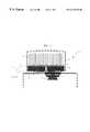
- FIG. 2is an enlarged side view of a probecard assembly used in the tester of FIG. 1;
- FIG. 3is a bottom plan view of a probecard along line 3 — 3 of FIG. 2;
- FIG. 4is an enlarged partial bottom plan view, not to scale, of the contact array of FIG. 3;
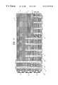
- FIG. 5is a cross-sectional view along line 5 — 5 of FIG. 4;
- FIG. 6Ais a partial cross-sectional view along line 6 A— 6 A of FIG. 5;
- FIG. 6Bis a partial cross-sectional view along line 6 B— 6 B of FIG. 5;
- FIG. 7is a flowchart showing the steps employed in manufacturing the probecard of the present invention according to one embodiment.
- FIG. 8is a view similar to FIG. 6B illustrating a further embodiment of the present invention.
- an automatic test systemincludes a computer-driven test controller 12 , and a test head 14 connected to the controller by a heavy-duty multi-cable 16 .
- the test headgenerally comprises a plurality of channel cards 18 that mount pin electronics (not shown) necessary to generate the test signals or patterns to each input pin or contact of a plurality of DUTs (not shown).
- a vertical translator board 22carries the channel cards and routs respective channel signals to a probecard assembly, generally designated 24 , that physically engages a wafer 26 .
- the probecard assembly 24includes a multi-layered disk-shaped probecard 30 (FIGS. 3 - 5 ), fixed in a multi-point alignment fixture with a microspring-tipped probe pin interface 32 available, for example, from Formfactor Inc., Livermore Calif.
- the alignment fixturepreferably includes a three-point planarizer 34 as more fully disclosed in U.S. Pat. No. 5,821,764, titled “Interface Apparatus For Automatic Test Equipment”, assigned to the assignee of the present invention and expressly incorporated herein by reference.
- a resilient microspring interposer 36is disposed between the probecard and the prober.
- the probecard 30enables efficient routing of signal traces or paths 46 (FIGS. 4 and 5) between selected sets of staggered vias 52 (FIGS. 4 and 5 ). This minimizes the number of signal layers 44 required to rout the test signals between the automatic test system and the array of DUT's. Because each layer of the probecard is of a minimal thickness, eliminating any additional layers preserves compatibility with existing mounting hardware that supports probecard standard thicknesses.
- the top layer (in phantom) of the probecard 30defines an engagement surface layer that includes a planar fiberglass substrate formed with a peripheral annular array of copper contact pads 40 etched or deposited on the top of the card as is well known in the art.
- a second contact surface 38that includes a square or rectangular-shaped array of individually isolated probe contacts 42 for interfacing with the matching backside (not shown) of the probe pin interface 32 .
- the probe contact arraycomprises a 52 ⁇ 52 matrix, totaling 2704 contacts, but may be varied in number and size depending on the application. The contacts are separated on a grid of approximately 0.046 inches.
- a significant factor involved in the probecard construction, visually exemplified in FIG. 3,is the relative spaced-apart nature of the contact pads that individually require electrical connections to the densely packed array of probe contacts.
- the present inventioncarries out this critical electrical routing in three dimensions as more fully described below.
- the signal layers 44are sandwiched between respective ground layers 50 . This characterizes each signal path as a predictable and relatively stable 50 ohm transmission line as is well known in the art.
- additional power layersare also included in the probecard 30 . Preferably, about thirty-four layers are utilized to construct a probecard with an overall thickness of approximately 0.25 inches. Of these layers, only about ten are available for signal routing.
- trace dimensionsAnother factor necessary to maintain the proper signal impedance along each signal path involves the trace dimensions.
- Current 50 ohm design considerationsrequire trace widths no less than approximately 0.005 to 0.008 inches, with spacings between traces no less than about 0.008 inches. Moreover, the spacings between ground planes are preferably set at approximately 0.015 inches apart. These requirements ensure minimal signal coupling, minimal cross-talk, and a 50 ohm trace.
- the conductive vias 52are formed in each layer, and are arranged to include varying staggered heights and diameters.
- the viasconnect to each prober contact 42 .
- the viasjoin the respective pattern traces 46 of each signal layer 44 to the proper sets of contact pads 40 and prober contacts 42 .
- a preferred configuration of the staggered via constructionemploys relatively long (approximately 0.25 inch) and thick (approximately 0.025 inch diameter) vias in a center subsection 54 of the probe contact array 42 .
- Progressively shorter and thinner subsections of viasare grouped in additional subsections 56 and 58 as the array expands outwardly from the center subsection.
- the subsectionsresult from the lamination of a plurality of board-sets 64 , 66 and 68 . Fabrication of the board-sets to achieve this construction is more fully described below.
- FIGS. 4 and 5are not to scale and show a simplified construction of the present invention for purposes of clarity.
- the staggered via architecture of the present inventionthat results from the laminated board-sets provides the capability of forming additional traces on the top signal layers 70 , 72 and 74 (FIG. 5) of the respective board-sets 64 , 66 and 68 (FIG. 5 ).
- This is an important feature of the present inventionbecause it allows additional traces to be routed on the top signal layers of the respective board-sets, thereby maximizing the trace density on those layers, and minimizing the overall number of layers in the probe card.
- Manufacture of the probecard 30 of the present inventionis carried out by a unique series of steps that ensures proper fabrication of the staggered vias 52 .
- the processgenerally involves fabricating a plurality of multi-layered board-sets, and laminating the board-sets together to form the probe card.
- any subsequent layersare added one-by-one in a “top-down” approach.
- This top-down methodologybegins by forming an initial core substrate, at step 100 .
- the core substratepreferably comprises a fully-baked material such as GETEC, Teflon or FR4.
- Microstrip materialis then deposited on the core material, at step 102 , to form a conductive layer.
- the microstripis exposed to an etching procedure, at step 104 , to define a predetermined signal path pattern. After the pattern is formed, a layer of half-baked pre-preg material is applied over the pattern, at step 106 .
- a second layer of conductive microstrip materialis then deposited over the pre-peg, at step 108 , to form a ground plane.
- a subsequent core substrateis then deposited over the ground plane, at step 110 , followed by steps 102 , 104 , 106 and 108 . This sequence is repeated until the board-set layers are all formed, at step 112 . Preferably, this occurs after fabrication of about six signal layers.
- one or more sets of throughboresare formed through the board-set layers to define the vias, at step 114 .
- a plating and filling operationis then carried out, at step 116 , to plate and fill the vias with a conductive material.
- the new board-setis laminated to the previously constructed board-set, at step 118 .
- the respective via constructions in the respective board-setscooperate to define sub-sections of vias that resemble a “pyramid” shape (FIG. 4 ).
- the probe cardis complete after a plurality of board-sets have been laminated in this top-down approach.
- the completed probe card 30is then secured within the alignment fixture 34 (FIG. 1) to form a part of the probe card assembly 24 .
- the alignment fixtureis of a standardized construction, the overall thickness of the probe card must be within a standardized thickness on the order of approximately 0.25 inches.
- the present inventionpreserves the standardized probecard thickness to avoid the necessity of redesigning the alignment fixture, thereby reducing overall costs.
- the probecard assembly 24is systematically registered over and touched-down onto arrays of DUT's on the wafer 26 by the test head 14 in a “step-and-repeat” fashion.
- the test controller 12issues commands for the pin electronics 18 to generate high frequency test signals on the order of from 125 MHz to 1.6 GHz.
- the signalsare fed through the probecard 30 for application to the input pins of the DUT's.
- Output signals from the DUT's that are generated in response to the applied vectorsare captured by selected contacts and routed back through the probecard to the test controller where they are analyzed.
- the analysisincludes, among other tests, a comparison of the captured waveforms to expected waveforms to verify proper operability of the DUT's.
- a second embodiment of the present inventionimproves the bandwidth performance of the probe card even further by tailoring the structure of the microstrip traces 200 that pass between adjacent vias 202 .
- the overall construction of the probe card according to the second embodimentis substantially similar to that of the first embodiment.
- the microstrip traces that pass between viasare formed with a tapered section 204 that necks down from a 50 ohm section 206 to a thinner transmision line with a higher characteristic impedance.
- the inventorhas discovered that tapering the microstrip traces causes an increase in inductance along the trace. This inductive characteristic offsets any undesirable frequency response effects that result from excess capacitance created by the formed via-trace terminations. The result is a more “ideal” 50 ohm transmission line characteristic in the 50 ohm section 206 , which allows higher frequency propagation with little attenuation.
- a further advantage afforded by the present inventioninvolves the superior bandwidth performance.
- the construction of the probe cardprovides the capability of routing high frequency signals on the order of up to 125 MHz to 250 MHz with minimal attenuation. This is realized by substantially maintaining a 50 ohm transmission line characteristic for each signal path trace.
Landscapes
- Engineering & Computer Science (AREA)
- Physics & Mathematics (AREA)
- General Physics & Mathematics (AREA)
- Microelectronics & Electronic Packaging (AREA)
- Power Engineering (AREA)
- General Engineering & Computer Science (AREA)
- Measuring Leads Or Probes (AREA)
- Testing Or Measuring Of Semiconductors Or The Like (AREA)
Abstract
Description
Claims (15)
Priority Applications (7)
| Application Number | Priority Date | Filing Date | Title |
|---|---|---|---|
| US09/178,247US6215320B1 (en) | 1998-10-23 | 1998-10-23 | High density printed circuit board |
| JP2000578664AJP3974752B2 (en) | 1998-10-23 | 1999-10-19 | High density printed circuit board and method of manufacturing the same |
| PCT/US1999/024342WO2000025141A1 (en) | 1998-10-23 | 1999-10-19 | High density printed circuit board |
| KR1020017005044AKR100703135B1 (en) | 1998-10-23 | 1999-10-19 | High density printed circuit board |
| EP99955010AEP1123512B1 (en) | 1998-10-23 | 1999-10-19 | High density printed circuit board |
| DE69917312TDE69917312T2 (en) | 1998-10-23 | 1999-10-19 | A HIGH LADDER DENSITY LADDER PLATE ASSEMBLY |
| TW088118282ATW535478B (en) | 1998-10-23 | 1999-10-22 | High density printed circuit board |
Applications Claiming Priority (1)
| Application Number | Priority Date | Filing Date | Title |
|---|---|---|---|
| US09/178,247US6215320B1 (en) | 1998-10-23 | 1998-10-23 | High density printed circuit board |
Publications (1)
| Publication Number | Publication Date |
|---|---|
| US6215320B1true US6215320B1 (en) | 2001-04-10 |
Family
ID=22651799
Family Applications (1)
| Application Number | Title | Priority Date | Filing Date |
|---|---|---|---|
| US09/178,247Expired - LifetimeUS6215320B1 (en) | 1998-10-23 | 1998-10-23 | High density printed circuit board |
Country Status (7)
| Country | Link |
|---|---|
| US (1) | US6215320B1 (en) |
| EP (1) | EP1123512B1 (en) |
| JP (1) | JP3974752B2 (en) |
| KR (1) | KR100703135B1 (en) |
| DE (1) | DE69917312T2 (en) |
| TW (1) | TW535478B (en) |
| WO (1) | WO2000025141A1 (en) |
Cited By (56)
| Publication number | Priority date | Publication date | Assignee | Title |
|---|---|---|---|---|
| US20020043980A1 (en)* | 2000-08-24 | 2002-04-18 | Rincon Reynaldo M. | Multiple-chip probe and universal tester contact assemblage |
| US6407344B1 (en)* | 1999-08-06 | 2002-06-18 | Shinko Electric Industries Co., Ltd | Multilayer circuit board |
| US6441488B1 (en)* | 1997-05-30 | 2002-08-27 | Tessera, Inc. | Fan-out translator for a semiconductor package |
| US20020132501A1 (en)* | 2001-03-16 | 2002-09-19 | Eldridge Benjamin N. | Wafer level interposer |
| US20020197895A1 (en)* | 1999-08-17 | 2002-12-26 | Formfactor, Inc. | Electrical contractor, especially wafer level contactor, using fluid pressure |
| US20030010976A1 (en)* | 2001-07-11 | 2003-01-16 | Formfactor, Inc. | Method of manufacturing a probe card |
| WO2003007003A1 (en)* | 2001-07-11 | 2003-01-23 | Formfactor, Inc. | Method of manufacturing a probe card |
| US6566899B2 (en)* | 2000-03-28 | 2003-05-20 | Kabushiki Kaisha Toshiba | Tester for semiconductor device |
| US6570397B2 (en) | 2001-08-07 | 2003-05-27 | Agilent Technologies, Inc. | Timing calibration and timing calibration verification of electronic circuit testers |
| US20030099097A1 (en)* | 2001-11-27 | 2003-05-29 | Sammy Mok | Construction structures and manufacturing processes for probe card assemblies and packages having wafer level springs |
| US6615485B2 (en) | 1993-11-16 | 2003-09-09 | Formfactor, Inc. | Probe card assembly and kit, and methods of making same |
| US6624648B2 (en)* | 1993-11-16 | 2003-09-23 | Formfactor, Inc. | Probe card assembly |
| US6724209B1 (en)* | 2000-04-13 | 2004-04-20 | Ralph G. Whitten | Method for testing signal paths between an integrated circuit wafer and a wafer tester |
| US20040140824A1 (en)* | 2003-01-18 | 2004-07-22 | Joon-Su Ji | Probe card |
| US20040223309A1 (en)* | 2000-05-23 | 2004-11-11 | Haemer Joseph Michael | Enhanced compliant probe card systems having improved planarity |
| US20040228100A1 (en)* | 2003-05-14 | 2004-11-18 | Wright Mitchel E. | Tailoring impedances of conductive traces in a circuit board |
| US20040268182A1 (en)* | 2003-06-12 | 2004-12-30 | Win-Harn Liu | Multithread auto test method |
| US20050156613A1 (en)* | 2004-01-20 | 2005-07-21 | Hisatomi Hosaka | Probe card |
| US6937037B2 (en) | 1995-11-09 | 2005-08-30 | Formfactor, Et Al. | Probe card assembly for contacting a device with raised contact elements |
| US20050275418A1 (en)* | 2000-05-23 | 2005-12-15 | Chong Fu C | High density interconnect system having rapid fabrication cycle |
| US20060001435A1 (en)* | 2004-06-30 | 2006-01-05 | Teneketges Nicholas J | Automated test equipment with DIB mounted three dimensional tester electronics bricks |
| US20060186906A1 (en)* | 2000-05-23 | 2006-08-24 | Bottoms W R | High density interconnect system for IC packages and interconnect assemblies |
| US20070017092A1 (en)* | 2005-07-22 | 2007-01-25 | Dutton Steven L | Method and apparatus for forming multi-layered circuits using liquid crystalline polymers |
| US20070057684A1 (en)* | 1999-05-27 | 2007-03-15 | Chong Fu C | Massively parallel interface for electronic circuit |
| US20070098895A1 (en)* | 2001-08-24 | 2007-05-03 | Smith Donald L | Method and Apparatus for Producing Uniform, Isotropic Stresses in a Sputtered Film |
| US20070205780A1 (en)* | 2006-03-06 | 2007-09-06 | Formfactor, Inc. | Stacked Guard Structures |
| US20080090429A1 (en)* | 2000-06-20 | 2008-04-17 | Sammy Mok | Systems for testing and packaging integrated circuits |
| US20080100317A1 (en)* | 1992-10-19 | 2008-05-01 | International Business Machines Corporation | High density integrated circuit apparatus, test probe and methods of use thereof |
| US20090146673A1 (en)* | 2007-12-05 | 2009-06-11 | Tokyo Electron Limited | Manufacturing method of probe card and the probe card |
| US20090189624A1 (en)* | 2008-01-28 | 2009-07-30 | Samsung Electronics Co., Ltd. | Interposer and a probe card assembly for electrical die sorting and methods of operating and manufacturing the same |
| US20090201041A1 (en)* | 2007-04-10 | 2009-08-13 | Microprobe, Inc. | Vertical Probe Array Arranged to Provide Space Transformation |
| US20090293274A1 (en)* | 2008-05-29 | 2009-12-03 | January Kister | Probe bonding method having improved control of bonding material |
| US20100013503A1 (en)* | 2008-07-15 | 2010-01-21 | Formfactor, Inc. | Dc test resource sharing for electronic device testing |
| US20100109691A1 (en)* | 2005-12-07 | 2010-05-06 | Microprobe, Inc. | Low Profile Probe Having Improved Mechanical Scrub and Reduced Contact Inductance |
| US20100182030A1 (en)* | 2004-05-21 | 2010-07-22 | Microprobe, Inc. | Knee Probe Having Reduced Thickness Section for Control of Scrub Motion |
| US20100220752A1 (en)* | 2009-03-02 | 2010-09-02 | Polaronyx, Inc. | 810 nm Ultra-Short Pulsed Fiber Laser |
| US20100244871A1 (en)* | 2009-02-24 | 2010-09-30 | Qualcomm Incorporated | Space transformer connector printed circuit board assembly |
| US20100289512A1 (en)* | 2004-07-09 | 2010-11-18 | Microprobe, Inc. | Probes with offset arm and suspension structure |
| US20110006796A1 (en)* | 2006-10-11 | 2011-01-13 | Microprobe, Inc. | Probe retention arrangement |
| US20110050274A1 (en)* | 2009-08-25 | 2011-03-03 | Aaron Durbin | Maintaining A Wafer/Wafer Translator Pair In An Attached State Free Of A Gasket Disposed Therebetween |
| US20110062978A1 (en)* | 2004-05-21 | 2011-03-17 | Microprobe, Inc. | Multiple contact probes |
| US7952373B2 (en) | 2000-05-23 | 2011-05-31 | Verigy (Singapore) Pte. Ltd. | Construction structures and manufacturing processes for integrated circuit wafer probe card assemblies |
| WO2012054201A1 (en)* | 2010-09-28 | 2012-04-26 | Advanced Inquiry Systems, Inc. | Wafer testing systems and associated methods of use and manufacture |
| USRE43503E1 (en) | 2006-06-29 | 2012-07-10 | Microprobe, Inc. | Probe skates for electrical testing of convex pad topologies |
| US8248091B2 (en) | 2006-10-20 | 2012-08-21 | Taiwan Semiconductor Manufacturing Co., Ltd. | Universal array type probe card design for semiconductor device testing |
| US20120264320A1 (en)* | 2011-04-13 | 2012-10-18 | Teradyne, Inc. | Probe-card interposer constructed using hexagonal modules |
| US8373428B2 (en) | 1993-11-16 | 2013-02-12 | Formfactor, Inc. | Probe card assembly and kit, and methods of making same |
| USRE44407E1 (en) | 2006-03-20 | 2013-08-06 | Formfactor, Inc. | Space transformers employing wire bonds for interconnections with fine pitch contacts |
| US8723546B2 (en) | 2007-10-19 | 2014-05-13 | Microprobe, Inc. | Vertical guided layered probe |
| US9097740B2 (en) | 2004-05-21 | 2015-08-04 | Formfactor, Inc. | Layered probes with core |
| US20150309074A1 (en)* | 2014-04-29 | 2015-10-29 | Taiwan Semiconductor Manufacturing Company Ltd. | Probe card |
| US9176186B2 (en) | 2009-08-25 | 2015-11-03 | Translarity, Inc. | Maintaining a wafer/wafer translator pair in an attached state free of a gasket disposed |
| US9476911B2 (en) | 2004-05-21 | 2016-10-25 | Microprobe, Inc. | Probes with high current carrying capability and laser machining methods |
| US11651910B2 (en) | 2020-12-10 | 2023-05-16 | Teradyne, Inc. | Inductance control system |
| US20230393174A1 (en)* | 2022-06-03 | 2023-12-07 | Formfactor, Inc. | Abbreviated Loopback Attenuation |
| US11862901B2 (en) | 2020-12-15 | 2024-01-02 | Teradyne, Inc. | Interposer |
Families Citing this family (6)
| Publication number | Priority date | Publication date | Assignee | Title |
|---|---|---|---|---|
| US6765400B2 (en)* | 2000-07-25 | 2004-07-20 | Ibiden Co., Ltd. | Inspection apparatus and probe card |
| US7759242B2 (en) | 2007-08-22 | 2010-07-20 | Qimonda Ag | Method of fabricating an integrated circuit |
| US8089331B2 (en) | 2009-05-12 | 2012-01-03 | Raytheon Company | Planar magnetic structure |
| US9632109B2 (en)* | 2011-06-30 | 2017-04-25 | Advantest Corporation | Methods, apparatus, and systems for contacting semiconductor dies that are electrically coupled to test access interface positioned in scribe lines of a wafer |
| US10049810B2 (en) | 2015-11-09 | 2018-08-14 | Raytheon Company | High voltage high frequency transformer |
| US10672553B2 (en) | 2017-05-10 | 2020-06-02 | Raytheon Company | High voltage high frequency transformer |
Citations (13)
| Publication number | Priority date | Publication date | Assignee | Title |
|---|---|---|---|---|
| US3739469A (en) | 1971-12-27 | 1973-06-19 | Ibm | Multilayer printed circuit board and method of manufacture |
| US4912399A (en)* | 1987-06-09 | 1990-03-27 | Tektronix, Inc. | Multiple lead probe for integrated circuits in wafer form |
| US5144228A (en) | 1991-04-23 | 1992-09-01 | International Business Machines Corporation | Probe interface assembly |
| US5162728A (en) | 1990-09-11 | 1992-11-10 | Cray Computer Corporation | Functional at speed test system for integrated circuits on undiced wafers |
| US5225777A (en) | 1992-02-04 | 1993-07-06 | International Business Machines Corporation | High density probe |
| US5336992A (en) | 1992-06-03 | 1994-08-09 | Trw Inc. | On-wafer integrated circuit electrical testing |
| JPH06302964A (en) | 1993-04-16 | 1994-10-28 | Oki Electric Ind Co Ltd | Circuit board for high-speed signal transmission |
| US5439732A (en)* | 1993-01-22 | 1995-08-08 | Nippondenso Co., Ltd. | Ceramic multi-layer wiring board |
| US5629631A (en) | 1994-04-15 | 1997-05-13 | International Business Machines Corporation | Interface card for a probe card assembly |
| US5665459A (en)* | 1995-03-06 | 1997-09-09 | Sumitomo Metal Ceramics Inc. | Low-temperature fired ceramic circuit substrate and thick-film paste for use in fabrication thereof |
| US5742174A (en) | 1995-11-03 | 1998-04-21 | Probe Technology | Membrane for holding a probe tip in proper location |
| EP0864870A2 (en) | 1988-05-16 | 1998-09-16 | LEEDY, Glenn J. | Method of making an integrated circuit testing device |
| US5949245A (en)* | 1997-02-01 | 1999-09-07 | Powership Semiconductor Corp. | Probe card with ground shield structure to minimize noise coupling effect during multiple-chip testing |
Family Cites Families (5)
| Publication number | Priority date | Publication date | Assignee | Title |
|---|---|---|---|---|
| JPS5824948B2 (en)* | 1977-08-08 | 1983-05-24 | 日本電信電話株式会社 | Manufacturing method of cross-wiring structure |
| JPH08255976A (en)* | 1995-03-15 | 1996-10-01 | Toshiba Corp | Multilayer wiring board |
| JPH0954116A (en)* | 1995-08-10 | 1997-02-25 | Nippon Denshi Zairyo Kk | High temperature probe card |
| JPH10135283A (en)* | 1996-10-31 | 1998-05-22 | Hitachi Chem Co Ltd | Inspection jig for semiconductor device |
| JPH10247783A (en)* | 1997-03-04 | 1998-09-14 | Ibiden Co Ltd | Multilayer printed wiring board and manufacture thereof |
- 1998
- 1998-10-23USUS09/178,247patent/US6215320B1/ennot_activeExpired - Lifetime
- 1999
- 1999-10-19JPJP2000578664Apatent/JP3974752B2/ennot_activeExpired - Lifetime
- 1999-10-19KRKR1020017005044Apatent/KR100703135B1/ennot_activeExpired - Fee Related
- 1999-10-19EPEP99955010Apatent/EP1123512B1/ennot_activeExpired - Lifetime
- 1999-10-19DEDE69917312Tpatent/DE69917312T2/ennot_activeExpired - Lifetime
- 1999-10-19WOPCT/US1999/024342patent/WO2000025141A1/enactiveIP Right Grant
- 1999-10-22TWTW088118282Apatent/TW535478B/ennot_activeIP Right Cessation
Patent Citations (13)
| Publication number | Priority date | Publication date | Assignee | Title |
|---|---|---|---|---|
| US3739469A (en) | 1971-12-27 | 1973-06-19 | Ibm | Multilayer printed circuit board and method of manufacture |
| US4912399A (en)* | 1987-06-09 | 1990-03-27 | Tektronix, Inc. | Multiple lead probe for integrated circuits in wafer form |
| EP0864870A2 (en) | 1988-05-16 | 1998-09-16 | LEEDY, Glenn J. | Method of making an integrated circuit testing device |
| US5162728A (en) | 1990-09-11 | 1992-11-10 | Cray Computer Corporation | Functional at speed test system for integrated circuits on undiced wafers |
| US5144228A (en) | 1991-04-23 | 1992-09-01 | International Business Machines Corporation | Probe interface assembly |
| US5225777A (en) | 1992-02-04 | 1993-07-06 | International Business Machines Corporation | High density probe |
| US5336992A (en) | 1992-06-03 | 1994-08-09 | Trw Inc. | On-wafer integrated circuit electrical testing |
| US5439732A (en)* | 1993-01-22 | 1995-08-08 | Nippondenso Co., Ltd. | Ceramic multi-layer wiring board |
| JPH06302964A (en) | 1993-04-16 | 1994-10-28 | Oki Electric Ind Co Ltd | Circuit board for high-speed signal transmission |
| US5629631A (en) | 1994-04-15 | 1997-05-13 | International Business Machines Corporation | Interface card for a probe card assembly |
| US5665459A (en)* | 1995-03-06 | 1997-09-09 | Sumitomo Metal Ceramics Inc. | Low-temperature fired ceramic circuit substrate and thick-film paste for use in fabrication thereof |
| US5742174A (en) | 1995-11-03 | 1998-04-21 | Probe Technology | Membrane for holding a probe tip in proper location |
| US5949245A (en)* | 1997-02-01 | 1999-09-07 | Powership Semiconductor Corp. | Probe card with ground shield structure to minimize noise coupling effect during multiple-chip testing |
Cited By (125)
| Publication number | Priority date | Publication date | Assignee | Title |
|---|---|---|---|---|
| US20080100317A1 (en)* | 1992-10-19 | 2008-05-01 | International Business Machines Corporation | High density integrated circuit apparatus, test probe and methods of use thereof |
| US7086149B2 (en) | 1993-11-16 | 2006-08-08 | Formfactor, Inc. | Method of making a contact structure with a distinctly formed tip structure |
| US8373428B2 (en) | 1993-11-16 | 2013-02-12 | Formfactor, Inc. | Probe card assembly and kit, and methods of making same |
| US6624648B2 (en)* | 1993-11-16 | 2003-09-23 | Formfactor, Inc. | Probe card assembly |
| US6615485B2 (en) | 1993-11-16 | 2003-09-09 | Formfactor, Inc. | Probe card assembly and kit, and methods of making same |
| US6937037B2 (en) | 1995-11-09 | 2005-08-30 | Formfactor, Et Al. | Probe card assembly for contacting a device with raised contact elements |
| US6441488B1 (en)* | 1997-05-30 | 2002-08-27 | Tessera, Inc. | Fan-out translator for a semiconductor package |
| US20070057684A1 (en)* | 1999-05-27 | 2007-03-15 | Chong Fu C | Massively parallel interface for electronic circuit |
| US20090153165A1 (en)* | 1999-05-27 | 2009-06-18 | Fu Chiung Chong | High Density Interconnect System Having Rapid Fabrication Cycle |
| US7403029B2 (en) | 1999-05-27 | 2008-07-22 | Nanonexus Corporation | Massively parallel interface for electronic circuit |
| US7772860B2 (en) | 1999-05-27 | 2010-08-10 | Nanonexus, Inc. | Massively parallel interface for electronic circuit |
| US7884634B2 (en) | 1999-05-27 | 2011-02-08 | Verigy (Singapore) Pte, Ltd | High density interconnect system having rapid fabrication cycle |
| US6407344B1 (en)* | 1999-08-06 | 2002-06-18 | Shinko Electric Industries Co., Ltd | Multilayer circuit board |
| US20020197895A1 (en)* | 1999-08-17 | 2002-12-26 | Formfactor, Inc. | Electrical contractor, especially wafer level contactor, using fluid pressure |
| US20090072848A1 (en)* | 1999-08-17 | 2009-03-19 | Formfactor, Inc. | Electrical Contactor, Especially Wafer Level Contactor, Using Fluid Pressure |
| US7967621B2 (en) | 1999-08-17 | 2011-06-28 | Formfactor, Inc. | Electrical contactor, especially wafer level contactor, using fluid pressure |
| US7195503B2 (en) | 1999-08-17 | 2007-03-27 | Formfactor, Inc. | Electrical contactor, especially wafer level contactor, using fluid pressure |
| US7455540B2 (en) | 1999-08-17 | 2008-11-25 | Formfactor, Inc. | Electrical contactor, especially wafer level contactor, using fluid pressure |
| US20100297863A1 (en)* | 1999-08-17 | 2010-11-25 | Formfactor, Inc. | Electrical contactor, especially wafer level contactor, using fluid pressure |
| US20070287304A1 (en)* | 1999-08-17 | 2007-12-13 | Formfactor, Inc. | Electrical Contactor, Espcecially Wafer Level Contactor, Using Fluid Pressure |
| US7722371B2 (en) | 1999-08-17 | 2010-05-25 | Formfactor, Inc. | Electrical contactor, especially wafer level contactor, using fluid pressure |
| US6566899B2 (en)* | 2000-03-28 | 2003-05-20 | Kabushiki Kaisha Toshiba | Tester for semiconductor device |
| US6724209B1 (en)* | 2000-04-13 | 2004-04-20 | Ralph G. Whitten | Method for testing signal paths between an integrated circuit wafer and a wafer tester |
| US7349223B2 (en) | 2000-05-23 | 2008-03-25 | Nanonexus, Inc. | Enhanced compliant probe card systems having improved planarity |
| US20040223309A1 (en)* | 2000-05-23 | 2004-11-11 | Haemer Joseph Michael | Enhanced compliant probe card systems having improved planarity |
| US7382142B2 (en) | 2000-05-23 | 2008-06-03 | Nanonexus, Inc. | High density interconnect system having rapid fabrication cycle |
| US7872482B2 (en) | 2000-05-23 | 2011-01-18 | Verigy (Singapore) Pte. Ltd | High density interconnect system having rapid fabrication cycle |
| US20050275418A1 (en)* | 2000-05-23 | 2005-12-15 | Chong Fu C | High density interconnect system having rapid fabrication cycle |
| US7952373B2 (en) | 2000-05-23 | 2011-05-31 | Verigy (Singapore) Pte. Ltd. | Construction structures and manufacturing processes for integrated circuit wafer probe card assemblies |
| US7579848B2 (en) | 2000-05-23 | 2009-08-25 | Nanonexus, Inc. | High density interconnect system for IC packages and interconnect assemblies |
| US20060186906A1 (en)* | 2000-05-23 | 2006-08-24 | Bottoms W R | High density interconnect system for IC packages and interconnect assemblies |
| US20080090429A1 (en)* | 2000-06-20 | 2008-04-17 | Sammy Mok | Systems for testing and packaging integrated circuits |
| US7621761B2 (en) | 2000-06-20 | 2009-11-24 | Nanonexus, Inc. | Systems for testing and packaging integrated circuits |
| US20060033516A1 (en)* | 2000-08-24 | 2006-02-16 | Rincon Reynaldo M | Multiple-chip probe and universal tester contact assemblage |
| US7026833B2 (en)* | 2000-08-24 | 2006-04-11 | Texas Instruments Incorporated | Multiple-chip probe and universal tester contact assemblage |
| US20020043980A1 (en)* | 2000-08-24 | 2002-04-18 | Rincon Reynaldo M. | Multiple-chip probe and universal tester contact assemblage |
| US6970005B2 (en)* | 2000-08-24 | 2005-11-29 | Texas Instruments Incorporated | Multiple-chip probe and universal tester contact assemblage |
| US20020132501A1 (en)* | 2001-03-16 | 2002-09-19 | Eldridge Benjamin N. | Wafer level interposer |
| US7396236B2 (en)* | 2001-03-16 | 2008-07-08 | Formfactor, Inc. | Wafer level interposer |
| US7649368B2 (en) | 2001-03-16 | 2010-01-19 | Formfactor, Inc. | Wafer level interposer |
| KR101062256B1 (en) | 2001-07-11 | 2011-09-06 | 폼팩터, 인크. | Probe Head, and Probe Card Assembly Method |
| US6729019B2 (en)* | 2001-07-11 | 2004-05-04 | Formfactor, Inc. | Method of manufacturing a probe card |
| US7948252B2 (en) | 2001-07-11 | 2011-05-24 | Formfactor, Inc. | Multilayered probe card |
| US20070126443A1 (en)* | 2001-07-11 | 2007-06-07 | Formfactor, Inc. | Method of Manufacturing A Probe Card |
| US20050146339A1 (en)* | 2001-07-11 | 2005-07-07 | Formfactor, Inc. | Method of manufacturing a probe card |
| EP1630563A1 (en)* | 2001-07-11 | 2006-03-01 | FormFactor, Inc. | Method of manufacturing a probe card |
| US20070247176A1 (en)* | 2001-07-11 | 2007-10-25 | Formfactor, Inc. | Method of Manufacturing a Probe Card |
| US6864105B2 (en) | 2001-07-11 | 2005-03-08 | Formfactor, Inc. | Method of manufacturing a probe card |
| US20030010976A1 (en)* | 2001-07-11 | 2003-01-16 | Formfactor, Inc. | Method of manufacturing a probe card |
| WO2003007003A1 (en)* | 2001-07-11 | 2003-01-23 | Formfactor, Inc. | Method of manufacturing a probe card |
| US20030025172A1 (en)* | 2001-07-11 | 2003-02-06 | Formfactor, Inc. | Method of manufacturing a probe card |
| US7196531B2 (en) | 2001-07-11 | 2007-03-27 | Formfactor, Inc. | Method of manufacturing a probe card |
| US7168162B2 (en) | 2001-07-11 | 2007-01-30 | Formfactor, Inc. | Method of manufacturing a probe card |
| US20080272794A1 (en)* | 2001-07-11 | 2008-11-06 | Formfactor, Inc.. | Method of manufacturing a probe card |
| US7400157B2 (en) | 2001-07-11 | 2008-07-15 | Formfactor, Inc. | Composite wiring structure having a wiring block and an insulating layer with electrical connections to probes |
| US6570397B2 (en) | 2001-08-07 | 2003-05-27 | Agilent Technologies, Inc. | Timing calibration and timing calibration verification of electronic circuit testers |
| US20070098895A1 (en)* | 2001-08-24 | 2007-05-03 | Smith Donald L | Method and Apparatus for Producing Uniform, Isotropic Stresses in a Sputtered Film |
| US20030099097A1 (en)* | 2001-11-27 | 2003-05-29 | Sammy Mok | Construction structures and manufacturing processes for probe card assemblies and packages having wafer level springs |
| US6917525B2 (en)* | 2001-11-27 | 2005-07-12 | Nanonexus, Inc. | Construction structures and manufacturing processes for probe card assemblies and packages having wafer level springs |
| EP1549962A4 (en)* | 2002-06-24 | 2005-12-14 | Nanonexus Inc | Construction structures and manufacturing processes for probe card assemblies and packages having wafer level springs |
| WO2004001807A3 (en)* | 2002-06-24 | 2004-12-23 | Nanonexus Inc | Construction structures and manufacturing processes for probe card assemblies and packages having wafer level springs |
| US20040140824A1 (en)* | 2003-01-18 | 2004-07-22 | Joon-Su Ji | Probe card |
| US6909297B2 (en)* | 2003-01-18 | 2005-06-21 | Samsung Electronics Co., Ltd. | Probe card |
| US7518884B2 (en) | 2003-05-14 | 2009-04-14 | Hewlett-Packard Development Company, L.P. | Tailoring impedances of conductive traces in a circuit board |
| US20040228100A1 (en)* | 2003-05-14 | 2004-11-18 | Wright Mitchel E. | Tailoring impedances of conductive traces in a circuit board |
| US7259968B2 (en) | 2003-05-14 | 2007-08-21 | Hewlett-Packard Development Company, L.P. | Tailoring impedances of conductive traces in a circuit board |
| US7111198B2 (en)* | 2003-06-12 | 2006-09-19 | Inventec Corporation | Multithread auto test method |
| US20040268182A1 (en)* | 2003-06-12 | 2004-12-30 | Win-Harn Liu | Multithread auto test method |
| US20050156613A1 (en)* | 2004-01-20 | 2005-07-21 | Hisatomi Hosaka | Probe card |
| WO2005115068A3 (en)* | 2004-05-20 | 2007-01-25 | Nanonexus Inc | High density interconnect system having rapid fabrication cycle |
| US8988091B2 (en) | 2004-05-21 | 2015-03-24 | Microprobe, Inc. | Multiple contact probes |
| US9097740B2 (en) | 2004-05-21 | 2015-08-04 | Formfactor, Inc. | Layered probes with core |
| US8111080B2 (en) | 2004-05-21 | 2012-02-07 | Microprobe, Inc. | Knee probe having reduced thickness section for control of scrub motion |
| US20100182030A1 (en)* | 2004-05-21 | 2010-07-22 | Microprobe, Inc. | Knee Probe Having Reduced Thickness Section for Control of Scrub Motion |
| US9316670B2 (en) | 2004-05-21 | 2016-04-19 | Formfactor, Inc. | Multiple contact probes |
| US9476911B2 (en) | 2004-05-21 | 2016-10-25 | Microprobe, Inc. | Probes with high current carrying capability and laser machining methods |
| US20110062978A1 (en)* | 2004-05-21 | 2011-03-17 | Microprobe, Inc. | Multiple contact probes |
| US7375542B2 (en) | 2004-06-30 | 2008-05-20 | Teradyne, Inc. | Automated test equipment with DIB mounted three dimensional tester electronics bricks |
| US7663389B2 (en) | 2004-06-30 | 2010-02-16 | Teradyne, Inc. | Automated test equipment with DIB mounted three dimensional tester electronics bricks |
| US20090079453A1 (en)* | 2004-06-30 | 2009-03-26 | Teneketges Nicholas J | Automated test equipment with dib mounted three dimensional tester electronics bricks |
| US20060001435A1 (en)* | 2004-06-30 | 2006-01-05 | Teneketges Nicholas J | Automated test equipment with DIB mounted three dimensional tester electronics bricks |
| US8203353B2 (en) | 2004-07-09 | 2012-06-19 | Microprobe, Inc. | Probes with offset arm and suspension structure |
| US20100289512A1 (en)* | 2004-07-09 | 2010-11-18 | Microprobe, Inc. | Probes with offset arm and suspension structure |
| US20070017092A1 (en)* | 2005-07-22 | 2007-01-25 | Dutton Steven L | Method and apparatus for forming multi-layered circuits using liquid crystalline polymers |
| US7290326B2 (en) | 2005-07-22 | 2007-11-06 | Dynaco Corp. | Method and apparatus for forming multi-layered circuits using liquid crystalline polymers |
| US20100109691A1 (en)* | 2005-12-07 | 2010-05-06 | Microprobe, Inc. | Low Profile Probe Having Improved Mechanical Scrub and Reduced Contact Inductance |
| US8415963B2 (en) | 2005-12-07 | 2013-04-09 | Microprobe, Inc. | Low profile probe having improved mechanical scrub and reduced contact inductance |
| US7944224B2 (en) | 2005-12-07 | 2011-05-17 | Microprobe, Inc. | Low profile probe having improved mechanical scrub and reduced contact inductance |
| US7956633B2 (en)* | 2006-03-06 | 2011-06-07 | Formfactor, Inc. | Stacked guard structures |
| US20070205780A1 (en)* | 2006-03-06 | 2007-09-06 | Formfactor, Inc. | Stacked Guard Structures |
| USRE44407E1 (en) | 2006-03-20 | 2013-08-06 | Formfactor, Inc. | Space transformers employing wire bonds for interconnections with fine pitch contacts |
| USRE43503E1 (en) | 2006-06-29 | 2012-07-10 | Microprobe, Inc. | Probe skates for electrical testing of convex pad topologies |
| US8907689B2 (en) | 2006-10-11 | 2014-12-09 | Microprobe, Inc. | Probe retention arrangement |
| US9310428B2 (en) | 2006-10-11 | 2016-04-12 | Formfactor, Inc. | Probe retention arrangement |
| US20110006796A1 (en)* | 2006-10-11 | 2011-01-13 | Microprobe, Inc. | Probe retention arrangement |
| US8248091B2 (en) | 2006-10-20 | 2012-08-21 | Taiwan Semiconductor Manufacturing Co., Ltd. | Universal array type probe card design for semiconductor device testing |
| US7952377B2 (en) | 2007-04-10 | 2011-05-31 | Microprobe, Inc. | Vertical probe array arranged to provide space transformation |
| US9274143B2 (en) | 2007-04-10 | 2016-03-01 | Formfactor, Inc. | Vertical probe array arranged to provide space transformation |
| US20090201041A1 (en)* | 2007-04-10 | 2009-08-13 | Microprobe, Inc. | Vertical Probe Array Arranged to Provide Space Transformation |
| US8324923B2 (en) | 2007-04-10 | 2012-12-04 | Microprobe, Inc. | Vertical probe array arranged to provide space transformation |
| US8723546B2 (en) | 2007-10-19 | 2014-05-13 | Microprobe, Inc. | Vertical guided layered probe |
| US8362792B2 (en)* | 2007-12-05 | 2013-01-29 | Tokyo Electron Limited | Manufacturing method of probe card and the probe card |
| US20090146673A1 (en)* | 2007-12-05 | 2009-06-11 | Tokyo Electron Limited | Manufacturing method of probe card and the probe card |
| US20090189624A1 (en)* | 2008-01-28 | 2009-07-30 | Samsung Electronics Co., Ltd. | Interposer and a probe card assembly for electrical die sorting and methods of operating and manufacturing the same |
| US8230593B2 (en) | 2008-05-29 | 2012-07-31 | Microprobe, Inc. | Probe bonding method having improved control of bonding material |
| US20090293274A1 (en)* | 2008-05-29 | 2009-12-03 | January Kister | Probe bonding method having improved control of bonding material |
| US20100013503A1 (en)* | 2008-07-15 | 2010-01-21 | Formfactor, Inc. | Dc test resource sharing for electronic device testing |
| US7924035B2 (en) | 2008-07-15 | 2011-04-12 | Formfactor, Inc. | Probe card assembly for electronic device testing with DC test resource sharing |
| US20100244871A1 (en)* | 2009-02-24 | 2010-09-30 | Qualcomm Incorporated | Space transformer connector printed circuit board assembly |
| US20100220752A1 (en)* | 2009-03-02 | 2010-09-02 | Polaronyx, Inc. | 810 nm Ultra-Short Pulsed Fiber Laser |
| US9146269B2 (en)* | 2009-08-25 | 2015-09-29 | Translarity, Inc. | Maintaining a wafer/wafer translator pair in an attached state free of a gasket diposed |
| US20110050274A1 (en)* | 2009-08-25 | 2011-03-03 | Aaron Durbin | Maintaining A Wafer/Wafer Translator Pair In An Attached State Free Of A Gasket Disposed Therebetween |
| US8362797B2 (en) | 2009-08-25 | 2013-01-29 | Advanced Inquiry Systems, Inc. | Maintaining a wafer/wafer translator pair in an attached state free of a gasket disposed therebetween |
| US9176186B2 (en) | 2009-08-25 | 2015-11-03 | Translarity, Inc. | Maintaining a wafer/wafer translator pair in an attached state free of a gasket disposed |
| US10571489B2 (en) | 2010-09-28 | 2020-02-25 | Translarity, Inc. | Wafer testing system and associated methods of use and manufacture |
| US9612259B2 (en) | 2010-09-28 | 2017-04-04 | Translarity, Inc. | Wafer testing system and associated methods of use and manufacture |
| US8405414B2 (en) | 2010-09-28 | 2013-03-26 | Advanced Inquiry Systems, Inc. | Wafer testing systems and associated methods of use and manufacture |
| WO2012054201A1 (en)* | 2010-09-28 | 2012-04-26 | Advanced Inquiry Systems, Inc. | Wafer testing systems and associated methods of use and manufacture |
| US20120264320A1 (en)* | 2011-04-13 | 2012-10-18 | Teradyne, Inc. | Probe-card interposer constructed using hexagonal modules |
| US8622752B2 (en)* | 2011-04-13 | 2014-01-07 | Teradyne, Inc. | Probe-card interposer constructed using hexagonal modules |
| US9759745B2 (en)* | 2014-04-29 | 2017-09-12 | Taiwan Semiconductor Manufacturing Company Ltd. | Probe card |
| US20150309074A1 (en)* | 2014-04-29 | 2015-10-29 | Taiwan Semiconductor Manufacturing Company Ltd. | Probe card |
| US11651910B2 (en) | 2020-12-10 | 2023-05-16 | Teradyne, Inc. | Inductance control system |
| US11862901B2 (en) | 2020-12-15 | 2024-01-02 | Teradyne, Inc. | Interposer |
| US20230393174A1 (en)* | 2022-06-03 | 2023-12-07 | Formfactor, Inc. | Abbreviated Loopback Attenuation |
Also Published As
| Publication number | Publication date |
|---|---|
| JP2002528904A (en) | 2002-09-03 |
| KR20010075660A (en) | 2001-08-09 |
| JP3974752B2 (en) | 2007-09-12 |
| EP1123512A1 (en) | 2001-08-16 |
| EP1123512B1 (en) | 2004-05-12 |
| DE69917312T2 (en) | 2005-05-12 |
| DE69917312D1 (en) | 2004-06-17 |
| TW535478B (en) | 2003-06-01 |
| KR100703135B1 (en) | 2007-04-05 |
| WO2000025141A1 (en) | 2000-05-04 |
Similar Documents
| Publication | Publication Date | Title |
|---|---|---|
| US6215320B1 (en) | High density printed circuit board | |
| KR101062256B1 (en) | Probe Head, and Probe Card Assembly Method | |
| EP1407280B1 (en) | Method of manufacturing a probe card | |
| US6911835B2 (en) | High performance probe system | |
| US6720501B1 (en) | PC board having clustered blind vias | |
| US3963986A (en) | Programmable interface contactor structure | |
| EP3095159A2 (en) | Wafer scale test interface unit: low loss and high isolation devices and methods for high speed and high density mixed signal interconnects and contactors | |
| JP2691809B2 (en) | Semiconductor device test equipment | |
| EP1454153A2 (en) | Flexible interface for a test head | |
| KR20220121849A (en) | Arrangement of coaxial vias on probe cards for automated test equipment | |
| US5781021A (en) | Universal fixtureless test equipment | |
| US6924637B2 (en) | Integrated circuit characterization printed circuit board, test equipment including same, method of fabrication thereof and method of characterizing an integrated circuit device | |
| KR20220121848A (en) | Arrangement of anterior vias on probe cards for automated test equipment | |
| US7388424B2 (en) | Apparatus for providing a high frequency loop back with a DC path for a parametric test | |
| JPH10246752A (en) | Device for connecting semiconductor chip |
Legal Events
| Date | Code | Title | Description |
|---|---|---|---|
| AS | Assignment | Owner name:TERADYNE, INC., MASSACHUSETTS Free format text:ASSIGNMENT OF ASSIGNORS INTEREST;ASSIGNOR:PARRISH, FRANK;REEL/FRAME:009544/0880 Effective date:19981022 | |
| STCF | Information on status: patent grant | Free format text:PATENTED CASE | |
| FPAY | Fee payment | Year of fee payment:4 | |
| FPAY | Fee payment | Year of fee payment:8 | |
| AS | Assignment | Owner name:BANK OF AMERICA, N.A., AS ADMINISTRATIVE AGENT, TE Free format text:NOTICE OF GRANT OF SECURITY INTEREST IN PATENTS;ASSIGNOR:TERADYNE, INC.;REEL/FRAME:021912/0762 Effective date:20081114 Owner name:BANK OF AMERICA, N.A., AS ADMINISTRATIVE AGENT,TEX Free format text:NOTICE OF GRANT OF SECURITY INTEREST IN PATENTS;ASSIGNOR:TERADYNE, INC.;REEL/FRAME:021912/0762 Effective date:20081114 | |
| AS | Assignment | Owner name:TERADYNE, INC, MASSACHUSETTS Free format text:RELEASE BY SECURED PARTY;ASSIGNOR:BANK OF AMERICA, N.A.;REEL/FRAME:022668/0750 Effective date:20090427 Owner name:TERADYNE, INC,MASSACHUSETTS Free format text:RELEASE BY SECURED PARTY;ASSIGNOR:BANK OF AMERICA, N.A.;REEL/FRAME:022668/0750 Effective date:20090427 | |
| FPAY | Fee payment | Year of fee payment:12 | |
| AS | Assignment | Owner name:BARCLAYS BANK PLC, NEW YORK Free format text:PATENT SECURITY AGREEMENT;ASSIGNORS:TERADYNE, INC.;LITEPOINT CORPORATION;REEL/FRAME:035507/0116 Effective date:20150427 | |
| AS | Assignment | Owner name:NEXTEST SYSTEMS CORPORATION, CALIFORNIA Free format text:RELEASE OF SECURITY INTEREST IN INTELLECTUAL PROPERTY;ASSIGNOR:BARCLAYS BANK PLC, AS COLLATERAL AGENT;REEL/FRAME:049632/0940 Effective date:20190627 Owner name:LITEPOINT CORPORATION, CALIFORNIA Free format text:RELEASE OF SECURITY INTEREST IN INTELLECTUAL PROPERTY;ASSIGNOR:BARCLAYS BANK PLC, AS COLLATERAL AGENT;REEL/FRAME:049632/0940 Effective date:20190627 Owner name:EAGLE TEST SYSTEMS, INC., ILLINOIS Free format text:RELEASE OF SECURITY INTEREST IN INTELLECTUAL PROPERTY;ASSIGNOR:BARCLAYS BANK PLC, AS COLLATERAL AGENT;REEL/FRAME:049632/0940 Effective date:20190627 Owner name:TERADYNE, INC., MASSACHUSETTS Free format text:RELEASE OF SECURITY INTEREST IN INTELLECTUAL PROPERTY;ASSIGNOR:BARCLAYS BANK PLC, AS COLLATERAL AGENT;REEL/FRAME:049632/0940 Effective date:20190627 Owner name:ENERGID TECHNOLOGIES CORPORATION, MASSACHUSETTS Free format text:RELEASE OF SECURITY INTEREST IN INTELLECTUAL PROPERTY;ASSIGNOR:BARCLAYS BANK PLC, AS COLLATERAL AGENT;REEL/FRAME:049632/0940 Effective date:20190627 Owner name:GENRAD, LLC, MASSACHUSETTS Free format text:RELEASE OF SECURITY INTEREST IN INTELLECTUAL PROPERTY;ASSIGNOR:BARCLAYS BANK PLC, AS COLLATERAL AGENT;REEL/FRAME:049632/0940 Effective date:20190627 | |
| AS | Assignment | Owner name:TRUIST BANK, GEORGIA Free format text:SECURITY INTEREST;ASSIGNOR:TERADYNE, INC.;REEL/FRAME:052595/0632 Effective date:20200501 |