US6215153B1 - MOSFET and method for fabricating the same - Google Patents
MOSFET and method for fabricating the sameDownload PDFInfo
- Publication number
- US6215153B1 US6215153B1US09/235,747US23574799AUS6215153B1US 6215153 B1US6215153 B1US 6215153B1US 23574799 AUS23574799 AUS 23574799AUS 6215153 B1US6215153 B1US 6215153B1
- Authority
- US
- United States
- Prior art keywords
- regions
- concentration
- insulation layers
- impurity regions
- semiconductor device
- Prior art date
- Legal status (The legal status is an assumption and is not a legal conclusion. Google has not performed a legal analysis and makes no representation as to the accuracy of the status listed.)
- Expired - Lifetime
Links
- 238000000034methodMethods0.000titleclaimsdescription18
- -1halo ionsChemical class0.000claimsabstractdescription11
- 239000012535impuritySubstances0.000claimsdescription73
- 239000000758substrateSubstances0.000claimsdescription50
- 239000004065semiconductorSubstances0.000claimsdescription45
- 238000009413insulationMethods0.000claimsdescription31
- 238000004519manufacturing processMethods0.000claimsdescription3
- 125000006850spacer groupChemical group0.000claimsdescription3
- 229910052581Si3N4Inorganic materials0.000claimsdescription2
- VYPSYNLAJGMNEJ-UHFFFAOYSA-NSilicium dioxideChemical compoundO=[Si]=OVYPSYNLAJGMNEJ-UHFFFAOYSA-N0.000claimsdescription2
- HQVNEWCFYHHQES-UHFFFAOYSA-Nsilicon nitrideChemical compoundN12[Si]34N5[Si]62N3[Si]51N64HQVNEWCFYHHQES-UHFFFAOYSA-N0.000claimsdescription2
- 229910052814silicon oxideInorganic materials0.000claimsdescription2
- 230000004888barrier functionEffects0.000abstractdescription14
- 238000009792diffusion processMethods0.000abstractdescription8
- 239000011810insulating materialSubstances0.000abstractdescription2
- 150000002500ionsChemical class0.000description9
- 230000008569processEffects0.000description9
- 229920002120photoresistant polymerPolymers0.000description8
- 229910021420polycrystalline siliconInorganic materials0.000description6
- 229920005591polysiliconPolymers0.000description6
- 238000005468ion implantationMethods0.000description5
- 238000000137annealingMethods0.000description2
- 238000001312dry etchingMethods0.000description2
- 238000001020plasma etchingMethods0.000description2
- 230000009467reductionEffects0.000description2
- XUIMIQQOPSSXEZ-UHFFFAOYSA-NSiliconChemical compound[Si]XUIMIQQOPSSXEZ-UHFFFAOYSA-N0.000description1
- 238000005530etchingMethods0.000description1
- 230000005669field effectEffects0.000description1
- 125000001475halogen functional groupChemical group0.000description1
- 230000010354integrationEffects0.000description1
- 229910044991metal oxideInorganic materials0.000description1
- 150000004706metal oxidesChemical class0.000description1
- 238000012986modificationMethods0.000description1
- 230000004048modificationEffects0.000description1
- 238000000059patterningMethods0.000description1
- 230000002265preventionEffects0.000description1
- 229910052710siliconInorganic materials0.000description1
- 239000010703siliconSubstances0.000description1
Images


Classifications
- H—ELECTRICITY
- H01—ELECTRIC ELEMENTS
- H01L—SEMICONDUCTOR DEVICES NOT COVERED BY CLASS H10
- H01L21/00—Processes or apparatus adapted for the manufacture or treatment of semiconductor or solid state devices or of parts thereof
- H01L21/02—Manufacture or treatment of semiconductor devices or of parts thereof
- H01L21/04—Manufacture or treatment of semiconductor devices or of parts thereof the devices having potential barriers, e.g. a PN junction, depletion layer or carrier concentration layer
- H01L21/18—Manufacture or treatment of semiconductor devices or of parts thereof the devices having potential barriers, e.g. a PN junction, depletion layer or carrier concentration layer the devices having semiconductor bodies comprising elements of Group IV of the Periodic Table or AIIIBV compounds with or without impurities, e.g. doping materials
- H—ELECTRICITY
- H10—SEMICONDUCTOR DEVICES; ELECTRIC SOLID-STATE DEVICES NOT OTHERWISE PROVIDED FOR
- H10D—INORGANIC ELECTRIC SEMICONDUCTOR DEVICES
- H10D30/00—Field-effect transistors [FET]
- H10D30/01—Manufacture or treatment
- H10D30/021—Manufacture or treatment of FETs having insulated gates [IGFET]
- H10D30/0223—Manufacture or treatment of FETs having insulated gates [IGFET] having source and drain regions or source and drain extensions self-aligned to sides of the gate
- H10D30/0227—Manufacture or treatment of FETs having insulated gates [IGFET] having source and drain regions or source and drain extensions self-aligned to sides of the gate having both lightly-doped source and drain extensions and source and drain regions self-aligned to the sides of the gate, e.g. lightly-doped drain [LDD] MOSFET or double-diffused drain [DDD] MOSFET
- H—ELECTRICITY
- H10—SEMICONDUCTOR DEVICES; ELECTRIC SOLID-STATE DEVICES NOT OTHERWISE PROVIDED FOR
- H10D—INORGANIC ELECTRIC SEMICONDUCTOR DEVICES
- H10D30/00—Field-effect transistors [FET]
- H10D30/60—Insulated-gate field-effect transistors [IGFET]
- H10D30/601—Insulated-gate field-effect transistors [IGFET] having lightly-doped drain or source extensions, e.g. LDD IGFETs or DDD IGFETs
- H—ELECTRICITY
- H10—SEMICONDUCTOR DEVICES; ELECTRIC SOLID-STATE DEVICES NOT OTHERWISE PROVIDED FOR
- H10D—INORGANIC ELECTRIC SEMICONDUCTOR DEVICES
- H10D62/00—Semiconductor bodies, or regions thereof, of devices having potential barriers
- H10D62/10—Shapes, relative sizes or dispositions of the regions of the semiconductor bodies; Shapes of the semiconductor bodies
- H10D62/113—Isolations within a component, i.e. internal isolations
- H10D62/115—Dielectric isolations, e.g. air gaps
- H10D62/116—Dielectric isolations, e.g. air gaps adjoining the input or output regions of field-effect devices, e.g. adjoining source or drain regions
Definitions
- the present inventionrelates to a semiconductor device, and more particularly, to a metal oxide silicon field effect transistor (MOSFET) and a method for fabricating the same.
- MOSFETmetal oxide silicon field effect transistor
- the reduction of the size of semiconductor devicesresults in high integration, especially the size of the transistors. Such a reduction reduces the channel lengths, which causes punch-through and increases leakage current between a source and a drain due to a shortened distance between the source and drain.
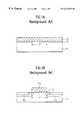
- FIGS. 1A-1Dillustrate processes for fabricating a MOSFET.
- an insulating filmis formed on an entire surface of the semiconductor substrate 11 and then patterned to form a gate insulating film 12 on a channel region 17 of the semiconductor substrate 11 .
- a polysilicon layer 13 for a gate electrodeis formed on the gate insulating film 12 .
- a photoresist(not shown) is coated on the polysilicon layer 13 . The photoresist is subjected to an exposure process and a development process for patterning the photoresist to define a gate electrode region.
- the polysilicon layer 13is selectively dry-etched using the patterned photoresist as a mask for dry-etching, thereby forming a gate electrode 13 a.
- Impurity ionsare implanted into the semiconductor substrate 11 using the gate electrode 13 a as a mask for ion-implantation, thereby forming LDD (Lightly Doped Drain) regions 14 in the surface of the semiconductor substrate 11 at both sides of the gate electrode 13 a .
- Ions having the first conductivity, same as the channelare implanted vertically or tiltly, to form first conductive impurity regions 14 a .
- the impurity regions 14 aimprove short channel characteristic.
- an insulating filmis formed on the entire surface of the substrate 11 including the gate electrode 13 a and then etched-back to form insulating sidewalls 15 at both sides of the gate electrode 13 a .
- impurity regions 16are formed as a sources and a drain D, as shown in FIG. 1 D.
- the process for fabricating a MOSFET according to the background arthas the following problem.
- the impurity ionsare implanted to form the halo regions for improving short channel characteristic, the impurity ions are implanted heavier at the edge portions than a center portion of the channel, thereby resulting in an increase of a threshold voltage and also changing the characteristic of a threshold voltage according to a length of the channel at the end.
- An object of the present inventionis to substantially obviate one or more of the problems due to limitations and disadvantages of the related art.
- An object of the present inventionis to provide an MOSFET and a method of fabricating the same which can prevent variation of a threshold voltage due to halo ions, thereby improving electrical characteristics of the MOSFET.
- the MOSFETincludes a first conductive type substrate, having a channel therein, a gate electrode formed on the channel region, a high concentration impurity regions of a second conductive type formed on the surface of the substrate and adjacent to both sides of the channel region, low concentration impurity regions of a second conductive type formed between the channel region and high concentration impurity regions, impurity regions of the first conductivity type formed beneath the low concentration impurity regions of the second conductive type and diffusion barriers formed between the low concentration impurity regions of the second conductive type and the impurity regions of the first conductive type.
- Another aspect of the present inventionincludes a method for fabricating an MOSFET including the steps of forming two diffusion barrier layers spaced from each other on an substrate of the first conductive type, growing an epitaxial layer on the entire surface of the substrate with a thickness enough to cover the barrier layers, forming a gate insulating film on a region of epitaxial layer and forming a gate electrode on the gate insulating film, implanting impurity-ions of a second conductive type having a low concentration into the epitaxial layer to form low concentration impurity regions of the second conductive type, implanting impurity-ions of the first conductive type into the substrate to form impurity regions of the first conductive type and implanting impurity-ions the second conductive type having a high concentration into the epitaxial layer including the substrate to form high concentration impurity regions in the surface of the epitaxial layer and at both sides of the gate electrode.
- the present inventioncan be achieved in a whole or in parts by a semiconductor device, comprising: a substrate; a control electrode insulatively formed over the substrate; first and second impurity regions of a first conductivity type formed in the substrate and substantially adjacent to first and second sides, respectively, of the control electrode, each of the first and second impurity regions having first and second concentration regions; a third impurity region of a second conductivity type formed beneath the first concentration region of the first and second impurity regions; and an insulation layer formed between the third impurity region and the first concentration region of the first and second impurity regions.
- the present inventioncan be also achieved in a whole or in parts by a method of making a semiconductor device, the method comprising the steps of: forming two insulation layers spaced from each other on a semiconductor substrate; forming a semiconductor layer on the entire surface of the semiconductor substrate with a thickness enough to cover the two insulation layers; forming a gate insulating film on a region of the semiconductor layer and forming a gate electrode on the gate insulating film; forming first impurity regions in the semiconductor layer and substantially next to opposing sides of the gate electrode, each first impurity region including an impurity portion formed over a corresponding one of the two insulation layers; forming second impurity regions beneath the two insulation layers.
- FIGS. 1A to 1 Dillustrates a process for fabricating a MOSFET according to a background art
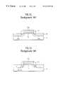
- FIG. 2illustrates a sectional view of an MOSFET according to the present invention
- FIGS. 3A to 3 Dillustrates a process for fabricating a MOSFET according to the present invention.
- the MOSFET in accordance with a preferred embodiment of the present inventionincludes a semiconductor substrate 21 of P-conductive type having a channel region 29 in the surface of the substrate 21 , a gate insulating film 23 formed on the channel region 29 , a gate electrode 24 formed on the gate insulating film 23 , sidewall spacers 27 formed at both sides of the gate electrode 24 and the gate insulating film 23 .
- High concentration impurity regions 28 of a N-conductive typeare formed in the surface of the substrate 21 and adjacent to both sides of the channel region 29 , and low concentration impurity regions 25 of N-conductive type are formed in the surface of the substrate 21 between the channel region 29 and the high concentration impurity regions 28 of N-conductive type.
- Impurity regions 26 of the P-conductive typeare formed beneath the low concentration impurity regions 25 of the N-conductive type, and diffusion barriers 22 are formed between the low concentration impurity regions of the N-conductive type and the impurity regions of the P-conductive type.
- the substratemay be just a semiconductor substrate or an epitaxial layer formed on the semiconductor substrate.
- FIGS. 3A-3Dillustrates a process steps of fabricating a MOSFET in accordance with a preferred embodiment of the present invention.
- an insulating filmis formed on a P-conductive type semiconductor substrate 21 and selectively removed, to form two barrier layers 22 spaced from each other by a prescribed distance on the substrate 21 .
- the barrier layers 22are made of an insulating material such as silicon oxide and silicon nitride.
- an epitaxial layer 21 ais grown using the substrate 21 as a seed layer and has sufficient thickness to cover the barrier layers 22 .
- a gate insulating film 23 and a gate electrode 24are formed on a region of the epitaxial layer 24 a .
- the regionis corresponding to a channel region 29 .
- a polysilicon layer(not shown) is formed thereon and photoresist (not shown) is coated on the polysilicon layer.
- the photoresistis patterned by subjecting the photoresist to exposure and development process. As a result, a photoresist pattern is used as a mask for selectively etching the polysilicon layer and the gate insulating film until a surface of the epitaxial layer 21 a is exposed.
- impurity ions of N-conductive typeare implanted into the surface of the epitaxial layer 21 a using the gate electrode 24 as a mask for ion-implantation, thereby forming lightly doped drain (LDD) regions 25 in the surface of the epitaxial layer 21 a at both sides of the gate electrode 24 .
- LDDlightly doped drain
- halo ions of P-conductive typeare implanted using the gate electrode 24 as a mask for ion-implantation, to form P-conductive type impurity regions 26 in the surface of the semiconductor substrate 21 beneath the barrier layers 22 .
- barrier layers 22serve as diffusion barriers which prevent the halo ions from being diffused to the edge portions of the gate electrode 24 during a following annealing process for diffusion of ions.
- the halo ionshas P-conductive type, which is a conductivity opposite to N-conductive type of the source and drain regions to be formed later, and are implanted tiltly or vertically.
- an insulating filmis formed on the whole exposed surface of the epitaxial layer 21 a including the gate electrode 24 and the gate insulating layer 23 .
- the insulating filmis then etched back to form insulating sidewalls 27 at both sides of the gate electrode 24 .
- a dry etchingsuch as Reactive Ion Etching (RIE) is used.
- N-conductive type impurity ionsare heavily implanted into the P-type substrate 21 using the gate electrode 24 and the insulating sidewalls 27 as masks during ion-implantation.
- the substrate 21is then subjected to an annealing process to form N-conductive type source and drain regions 28 in the semiconductor substrate 21 and the epitaxial layer 21 a at both sides of the gate electrode 24 .
- the source and drain regions 28have a higher concentration than the LDD regions 25 .
- the barrier layers 22block the halo ions, having P-conductive type, from being diffused to the edge portions of the gate electrode 24 . Because the epitaxial layer 21 a is grown using the substrate 21 , the epitaxial layer 21 a may be regarded as a part of the substrate 21 and also it has a same conductive type as the substrate 21 .
- the MOSFET and the method for fabricating a MOSFET of the present inventionhave various advantages. As diffusion of the halo ions to an edge portion of the gate electrode is prevented in the halo ion diffusion, the halo ions being injected for improving short channel characteristic by forming barrier layers in the semiconductor substrate below edge portion of the gate electrode, an increase of a threshold voltage of the device can be prevented. This prevention of threshold voltage variation improves electrical characteristics of the device.
Landscapes
- Engineering & Computer Science (AREA)
- Physics & Mathematics (AREA)
- Condensed Matter Physics & Semiconductors (AREA)
- General Physics & Mathematics (AREA)
- Manufacturing & Machinery (AREA)
- Computer Hardware Design (AREA)
- Microelectronics & Electronic Packaging (AREA)
- Power Engineering (AREA)
- Insulated Gate Type Field-Effect Transistor (AREA)
Abstract
Description
Claims (19)
Applications Claiming Priority (2)
| Application Number | Priority Date | Filing Date | Title |
|---|---|---|---|
| KR1019980002328AKR100257074B1 (en) | 1998-01-26 | 1998-01-26 | Mosfet and method for manufacturing the same |
| KR98-2328 | 1998-01-26 |
Publications (1)
| Publication Number | Publication Date |
|---|---|
| US6215153B1true US6215153B1 (en) | 2001-04-10 |
Family
ID=19532127
Family Applications (1)
| Application Number | Title | Priority Date | Filing Date |
|---|---|---|---|
| US09/235,747Expired - LifetimeUS6215153B1 (en) | 1998-01-26 | 1999-01-25 | MOSFET and method for fabricating the same |
Country Status (4)
| Country | Link |
|---|---|
| US (1) | US6215153B1 (en) |
| JP (1) | JP3049496B2 (en) |
| KR (1) | KR100257074B1 (en) |
| DE (1) | DE19836953B4 (en) |
Cited By (1)
| Publication number | Priority date | Publication date | Assignee | Title |
|---|---|---|---|---|
| WO2012079463A1 (en)* | 2010-12-16 | 2012-06-21 | Csmc Technologies Fab1 Co., Ltd | Cmos devices and method for manufacturing the same |
Families Citing this family (4)
| Publication number | Priority date | Publication date | Assignee | Title |
|---|---|---|---|---|
| US6437406B1 (en)* | 2000-10-19 | 2002-08-20 | International Business Machines Corporation | Super-halo formation in FETs |
| KR20030001942A (en)* | 2001-06-28 | 2003-01-08 | 동부전자 주식회사 | Semiconductor Device And Manufacturing Method For the Same |
| KR100487927B1 (en)* | 2003-07-21 | 2005-05-09 | 주식회사 하이닉스반도체 | A method for manufacturing of a Magnetic random access memory |
| KR100818403B1 (en)* | 2006-09-28 | 2008-04-01 | 동부일렉트로닉스 주식회사 | MOS transistor manufacturing method |
Citations (12)
| Publication number | Priority date | Publication date | Assignee | Title |
|---|---|---|---|---|
| US4700454A (en) | 1985-11-04 | 1987-10-20 | Intel Corporation | Process for forming MOS transistor with buried oxide regions for insulation |
| US4810664A (en) | 1986-08-14 | 1989-03-07 | Hewlett-Packard Company | Method for making patterned implanted buried oxide transistors and structures |
| US4837186A (en)* | 1984-08-31 | 1989-06-06 | Kabushiki Kaisha Toshiba | Silicon semiconductor substrate with an insulating layer embedded therein and method for forming the same |
| US4908681A (en)* | 1980-04-30 | 1990-03-13 | Sanyo Electric Co., Ltd. | Insulated gate field effect transistor with buried layer |
| US5049992A (en) | 1990-08-27 | 1991-09-17 | Zenith Electronics Corporation | HDTV system with receivers operable at different levels of resolution |
| US5262854A (en) | 1992-02-21 | 1993-11-16 | Rca Thomson Licensing Corporation | Lower resolution HDTV receivers |
| US5565925A (en) | 1992-10-26 | 1996-10-15 | Nec Corporation | Image sub-sampling apparatus |
| US5593928A (en) | 1993-11-30 | 1997-01-14 | Lg Semicon Co., Ltd. | Method of making a semiconductor device having floating source and drain regions |
| US5614952A (en) | 1994-10-11 | 1997-03-25 | Hitachi America, Ltd. | Digital video decoder for decoding digital high definition and/or digital standard definition television signals |
| US5641980A (en)* | 1995-06-16 | 1997-06-24 | Mitsubishi Denki Kabushiki Kaisha | Device having a high concentration region under the channel |
| US5712173A (en)* | 1996-01-24 | 1998-01-27 | Advanced Micro Devices, Inc. | Method of making semiconductor device with self-aligned insulator |
| US5977602A (en)* | 1997-12-19 | 1999-11-02 | Advanced Micro Devices | Semiconductor device having an oxygen-rich punchthrough region extending through the length of the active region |
Family Cites Families (3)
| Publication number | Priority date | Publication date | Assignee | Title |
|---|---|---|---|---|
| JPS59220972A (en)* | 1983-05-30 | 1984-12-12 | Mitsubishi Electric Corp | Mos type semiconductor device and manufacture thereof |
| JPS63115370A (en)* | 1986-11-04 | 1988-05-19 | Hitachi Ltd | Semiconductor device |
| US5245208A (en)* | 1991-04-22 | 1993-09-14 | Mitsubishi Denki Kabushiki Kaisha | Semiconductor device and manufacturing method thereof |
- 1998
- 1998-01-26KRKR1019980002328Apatent/KR100257074B1/ennot_activeExpired - Fee Related
- 1998-08-14DEDE19836953Apatent/DE19836953B4/ennot_activeExpired - Fee Related
- 1998-10-05JPJP10282288Apatent/JP3049496B2/ennot_activeExpired - Fee Related
- 1999
- 1999-01-25USUS09/235,747patent/US6215153B1/ennot_activeExpired - Lifetime
Patent Citations (12)
| Publication number | Priority date | Publication date | Assignee | Title |
|---|---|---|---|---|
| US4908681A (en)* | 1980-04-30 | 1990-03-13 | Sanyo Electric Co., Ltd. | Insulated gate field effect transistor with buried layer |
| US4837186A (en)* | 1984-08-31 | 1989-06-06 | Kabushiki Kaisha Toshiba | Silicon semiconductor substrate with an insulating layer embedded therein and method for forming the same |
| US4700454A (en) | 1985-11-04 | 1987-10-20 | Intel Corporation | Process for forming MOS transistor with buried oxide regions for insulation |
| US4810664A (en) | 1986-08-14 | 1989-03-07 | Hewlett-Packard Company | Method for making patterned implanted buried oxide transistors and structures |
| US5049992A (en) | 1990-08-27 | 1991-09-17 | Zenith Electronics Corporation | HDTV system with receivers operable at different levels of resolution |
| US5262854A (en) | 1992-02-21 | 1993-11-16 | Rca Thomson Licensing Corporation | Lower resolution HDTV receivers |
| US5565925A (en) | 1992-10-26 | 1996-10-15 | Nec Corporation | Image sub-sampling apparatus |
| US5593928A (en) | 1993-11-30 | 1997-01-14 | Lg Semicon Co., Ltd. | Method of making a semiconductor device having floating source and drain regions |
| US5614952A (en) | 1994-10-11 | 1997-03-25 | Hitachi America, Ltd. | Digital video decoder for decoding digital high definition and/or digital standard definition television signals |
| US5641980A (en)* | 1995-06-16 | 1997-06-24 | Mitsubishi Denki Kabushiki Kaisha | Device having a high concentration region under the channel |
| US5712173A (en)* | 1996-01-24 | 1998-01-27 | Advanced Micro Devices, Inc. | Method of making semiconductor device with self-aligned insulator |
| US5977602A (en)* | 1997-12-19 | 1999-11-02 | Advanced Micro Devices | Semiconductor device having an oxygen-rich punchthrough region extending through the length of the active region |
Cited By (1)
| Publication number | Priority date | Publication date | Assignee | Title |
|---|---|---|---|---|
| WO2012079463A1 (en)* | 2010-12-16 | 2012-06-21 | Csmc Technologies Fab1 Co., Ltd | Cmos devices and method for manufacturing the same |
Also Published As
| Publication number | Publication date |
|---|---|
| JP3049496B2 (en) | 2000-06-05 |
| KR100257074B1 (en) | 2000-05-15 |
| DE19836953A1 (en) | 1999-08-05 |
| KR19990066411A (en) | 1999-08-16 |
| JPH11220128A (en) | 1999-08-10 |
| DE19836953B4 (en) | 2009-06-18 |
Similar Documents
| Publication | Publication Date | Title |
|---|---|---|
| JP2826924B2 (en) | Method of manufacturing MOSFET | |
| US6881630B2 (en) | Methods for fabricating field effect transistors having elevated source/drain regions | |
| KR19980029024A (en) | MOSFET and manufacturing method | |
| KR100223847B1 (en) | Semiconductor device and method of manufacturing the same | |
| US5654215A (en) | Method for fabrication of a non-symmetrical transistor | |
| US5552329A (en) | Method of making metal oxide semiconductor transistors | |
| US6326665B1 (en) | Semiconductor device with insulating films | |
| EP0964454A1 (en) | Field-effect transistor having a lightly doped drain region and method of making the same | |
| US6008100A (en) | Metal-oxide semiconductor field effect transistor device fabrication process | |
| US6362060B2 (en) | Method for forming semiconductor device having a gate in the trench | |
| JPH1187704A (en) | Semiconductor device and manufacturing method thereof | |
| US6215153B1 (en) | MOSFET and method for fabricating the same | |
| JP2924947B2 (en) | Method for manufacturing semiconductor device | |
| KR960000229B1 (en) | Making method of vertical channel mosfet using trench structure | |
| JPH0818042A (en) | Method for manufacturing MOS transistor | |
| KR100349367B1 (en) | Method of manufacturing semiconductor device | |
| KR100198676B1 (en) | Transistor of semiconductor device and method of manufacturing the same | |
| JP3307972B2 (en) | Method for manufacturing field effect transistor and field effect transistor | |
| KR100320436B1 (en) | Method for manufacturing mosfet | |
| KR101004807B1 (en) | Structure of High Voltage Transistor of Curved Channel with Increased Channel Punch Resistance and Its Manufacturing Method | |
| JPH09181313A (en) | Method of manufacturing MOSFET | |
| US6936517B2 (en) | Method for fabricating transistor of semiconductor device | |
| KR0142787B1 (en) | Fabrication method of mosfet | |
| JPH11214682A (en) | Fabrication of semiconductor device | |
| KR940006705B1 (en) | Mosfet and manufacturing method thereof |
Legal Events
| Date | Code | Title | Description |
|---|---|---|---|
| AS | Assignment | Owner name:LG SEMICON CO., LTD., KOREA, REPUBLIC OF Free format text:ASSIGNMENT OF ASSIGNORS INTEREST;ASSIGNOR:PARK, SUNG KYE;REEL/FRAME:009757/0924 Effective date:19990118 | |
| AS | Assignment | Owner name:HYUNDAI ELECTRONICS INDUSTRIES CO., LTD., KOREA, R Free format text:MERGER;ASSIGNOR:LG SEMICON CO., LTD.;REEL/FRAME:011380/0852 Effective date:19991020 | |
| STCF | Information on status: patent grant | Free format text:PATENTED CASE | |
| FEPP | Fee payment procedure | Free format text:PAYOR NUMBER ASSIGNED (ORIGINAL EVENT CODE: ASPN); ENTITY STATUS OF PATENT OWNER: LARGE ENTITY | |
| FPAY | Fee payment | Year of fee payment:4 | |
| FPAY | Fee payment | Year of fee payment:8 | |
| FEPP | Fee payment procedure | Free format text:PAYER NUMBER DE-ASSIGNED (ORIGINAL EVENT CODE: RMPN); ENTITY STATUS OF PATENT OWNER: LARGE ENTITY Free format text:PAYOR NUMBER ASSIGNED (ORIGINAL EVENT CODE: ASPN); ENTITY STATUS OF PATENT OWNER: LARGE ENTITY | |
| FPAY | Fee payment | Year of fee payment:12 |