US6214652B1 - Thin film transistors and method of forming thin film transistors - Google Patents
Thin film transistors and method of forming thin film transistorsDownload PDFInfo
- Publication number
- US6214652B1 US6214652B1US09/442,340US44234099AUS6214652B1US 6214652 B1US6214652 B1US 6214652B1US 44234099 AUS44234099 AUS 44234099AUS 6214652 B1US6214652 B1US 6214652B1
- Authority
- US
- United States
- Prior art keywords
- thin film
- region
- polycrystalline
- drain
- forming
- Prior art date
- Legal status (The legal status is an assumption and is not a legal conclusion. Google has not performed a legal analysis and makes no representation as to the accuracy of the status listed.)
- Expired - Lifetime
Links
Images


Classifications
- H—ELECTRICITY
- H01—ELECTRIC ELEMENTS
- H01L—SEMICONDUCTOR DEVICES NOT COVERED BY CLASS H10
- H01L21/00—Processes or apparatus adapted for the manufacture or treatment of semiconductor or solid state devices or of parts thereof
- H01L21/02—Manufacture or treatment of semiconductor devices or of parts thereof
- H01L21/04—Manufacture or treatment of semiconductor devices or of parts thereof the devices having potential barriers, e.g. a PN junction, depletion layer or carrier concentration layer
- H01L21/18—Manufacture or treatment of semiconductor devices or of parts thereof the devices having potential barriers, e.g. a PN junction, depletion layer or carrier concentration layer the devices having semiconductor bodies comprising elements of Group IV of the Periodic Table or AIIIBV compounds with or without impurities, e.g. doping materials
- H01L21/26—Bombardment with radiation
- H01L21/263—Bombardment with radiation with high-energy radiation
- H01L21/265—Bombardment with radiation with high-energy radiation producing ion implantation
- H01L21/26506—Bombardment with radiation with high-energy radiation producing ion implantation in group IV semiconductors
- H—ELECTRICITY
- H01—ELECTRIC ELEMENTS
- H01L—SEMICONDUCTOR DEVICES NOT COVERED BY CLASS H10
- H01L21/00—Processes or apparatus adapted for the manufacture or treatment of semiconductor or solid state devices or of parts thereof
- H01L21/02—Manufacture or treatment of semiconductor devices or of parts thereof
- H01L21/04—Manufacture or treatment of semiconductor devices or of parts thereof the devices having potential barriers, e.g. a PN junction, depletion layer or carrier concentration layer
- H01L21/18—Manufacture or treatment of semiconductor devices or of parts thereof the devices having potential barriers, e.g. a PN junction, depletion layer or carrier concentration layer the devices having semiconductor bodies comprising elements of Group IV of the Periodic Table or AIIIBV compounds with or without impurities, e.g. doping materials
- H01L21/26—Bombardment with radiation
- H01L21/263—Bombardment with radiation with high-energy radiation
- H01L21/265—Bombardment with radiation with high-energy radiation producing ion implantation
- H01L21/2658—Bombardment with radiation with high-energy radiation producing ion implantation of a molecular ion, e.g. decaborane
- H—ELECTRICITY
- H10—SEMICONDUCTOR DEVICES; ELECTRIC SOLID-STATE DEVICES NOT OTHERWISE PROVIDED FOR
- H10D—INORGANIC ELECTRIC SEMICONDUCTOR DEVICES
- H10D30/00—Field-effect transistors [FET]
- H10D30/01—Manufacture or treatment
- H10D30/021—Manufacture or treatment of FETs having insulated gates [IGFET]
- H10D30/031—Manufacture or treatment of FETs having insulated gates [IGFET] of thin-film transistors [TFT]
- H10D30/0312—Manufacture or treatment of FETs having insulated gates [IGFET] of thin-film transistors [TFT] characterised by the gate electrodes
- H10D30/0314—Manufacture or treatment of FETs having insulated gates [IGFET] of thin-film transistors [TFT] characterised by the gate electrodes of lateral top-gate TFTs comprising only a single gate
- H—ELECTRICITY
- H10—SEMICONDUCTOR DEVICES; ELECTRIC SOLID-STATE DEVICES NOT OTHERWISE PROVIDED FOR
- H10D—INORGANIC ELECTRIC SEMICONDUCTOR DEVICES
- H10D30/00—Field-effect transistors [FET]
- H10D30/01—Manufacture or treatment
- H10D30/021—Manufacture or treatment of FETs having insulated gates [IGFET]
- H10D30/031—Manufacture or treatment of FETs having insulated gates [IGFET] of thin-film transistors [TFT]
- H10D30/0312—Manufacture or treatment of FETs having insulated gates [IGFET] of thin-film transistors [TFT] characterised by the gate electrodes
- H10D30/0316—Manufacture or treatment of FETs having insulated gates [IGFET] of thin-film transistors [TFT] characterised by the gate electrodes of lateral bottom-gate TFTs comprising only a single gate
- H—ELECTRICITY
- H10—SEMICONDUCTOR DEVICES; ELECTRIC SOLID-STATE DEVICES NOT OTHERWISE PROVIDED FOR
- H10D—INORGANIC ELECTRIC SEMICONDUCTOR DEVICES
- H10D30/00—Field-effect transistors [FET]
- H10D30/01—Manufacture or treatment
- H10D30/021—Manufacture or treatment of FETs having insulated gates [IGFET]
- H10D30/031—Manufacture or treatment of FETs having insulated gates [IGFET] of thin-film transistors [TFT]
- H10D30/0321—Manufacture or treatment of FETs having insulated gates [IGFET] of thin-film transistors [TFT] comprising silicon, e.g. amorphous silicon or polysilicon
- H—ELECTRICITY
- H10—SEMICONDUCTOR DEVICES; ELECTRIC SOLID-STATE DEVICES NOT OTHERWISE PROVIDED FOR
- H10D—INORGANIC ELECTRIC SEMICONDUCTOR DEVICES
- H10D30/00—Field-effect transistors [FET]
- H10D30/60—Insulated-gate field-effect transistors [IGFET]
- H10D30/67—Thin-film transistors [TFT]
- H10D30/6704—Thin-film transistors [TFT] having supplementary regions or layers in the thin films or in the insulated bulk substrates for controlling properties of the device
- H10D30/6713—Thin-film transistors [TFT] having supplementary regions or layers in the thin films or in the insulated bulk substrates for controlling properties of the device characterised by the properties of the source or drain regions, e.g. compositions or sectional shapes
- H10D30/6715—Thin-film transistors [TFT] having supplementary regions or layers in the thin films or in the insulated bulk substrates for controlling properties of the device characterised by the properties of the source or drain regions, e.g. compositions or sectional shapes characterised by the doping profiles, e.g. having lightly-doped source or drain extensions
- H10D30/6717—Thin-film transistors [TFT] having supplementary regions or layers in the thin films or in the insulated bulk substrates for controlling properties of the device characterised by the properties of the source or drain regions, e.g. compositions or sectional shapes characterised by the doping profiles, e.g. having lightly-doped source or drain extensions the source and the drain regions being asymmetrical
- H—ELECTRICITY
- H10—SEMICONDUCTOR DEVICES; ELECTRIC SOLID-STATE DEVICES NOT OTHERWISE PROVIDED FOR
- H10D—INORGANIC ELECTRIC SEMICONDUCTOR DEVICES
- H10D30/00—Field-effect transistors [FET]
- H10D30/60—Insulated-gate field-effect transistors [IGFET]
- H10D30/67—Thin-film transistors [TFT]
- H10D30/6729—Thin-film transistors [TFT] characterised by the electrodes
- H10D30/673—Thin-film transistors [TFT] characterised by the electrodes characterised by the shapes, relative sizes or dispositions of the gate electrodes
- H10D30/6731—Top-gate only TFTs
- H—ELECTRICITY
- H10—SEMICONDUCTOR DEVICES; ELECTRIC SOLID-STATE DEVICES NOT OTHERWISE PROVIDED FOR
- H10D—INORGANIC ELECTRIC SEMICONDUCTOR DEVICES
- H10D30/00—Field-effect transistors [FET]
- H10D30/60—Insulated-gate field-effect transistors [IGFET]
- H10D30/67—Thin-film transistors [TFT]
- H10D30/6729—Thin-film transistors [TFT] characterised by the electrodes
- H10D30/673—Thin-film transistors [TFT] characterised by the electrodes characterised by the shapes, relative sizes or dispositions of the gate electrodes
- H10D30/6732—Bottom-gate only TFTs
- H—ELECTRICITY
- H10—SEMICONDUCTOR DEVICES; ELECTRIC SOLID-STATE DEVICES NOT OTHERWISE PROVIDED FOR
- H10D—INORGANIC ELECTRIC SEMICONDUCTOR DEVICES
- H10D30/00—Field-effect transistors [FET]
- H10D30/60—Insulated-gate field-effect transistors [IGFET]
- H10D30/67—Thin-film transistors [TFT]
- H10D30/674—Thin-film transistors [TFT] characterised by the active materials
- H10D30/6741—Group IV materials, e.g. germanium or silicon carbide
- H10D30/6743—Silicon
- H10D30/6745—Polycrystalline or microcrystalline silicon
- H—ELECTRICITY
- H10—SEMICONDUCTOR DEVICES; ELECTRIC SOLID-STATE DEVICES NOT OTHERWISE PROVIDED FOR
- H10D—INORGANIC ELECTRIC SEMICONDUCTOR DEVICES
- H10D30/00—Field-effect transistors [FET]
- H10D30/60—Insulated-gate field-effect transistors [IGFET]
- H10D30/67—Thin-film transistors [TFT]
- H10D30/674—Thin-film transistors [TFT] characterised by the active materials
- H10D30/675—Group III-V materials, Group II-VI materials, Group IV-VI materials, selenium or tellurium
Definitions
- This inventionrelates to thin film transistors and to methods of forming thin film transistors.
- Field effect transistorshave typically been formed by providing active areas within a bulk substrate material or within a complementary conductivity le type well formed within a bulk substrate. Although the field effect transistor feature size is reducing with advances in process technology, even smaller transistors can be formed from thin films deposited over oxide. These transistors are commonly referred to as “thin film transistors” (TF 1 ).
- a thin film of semiconductive materialis first provided.
- a central channel region of the thin filmis masked, while opposing adjacent source/drain regions are doped with an appropriate p or n type conductivity enhancing impurity:
- a gate insulator and gateare provided either above or below the thin film channel region, thus providing a field effect transistor having an active channel region formed entirely within a thin film as opposed to a bulk substrate.
- a static memory cellis characterized by operation in one of two mutually exclusive and cell-maintaining operating states. Each operating state defines one of the two possible binary bit values, 0 or 1.
- a static memory celltypically has an output which reflects the operating state of the memory cell. Such an output produces a “high” voltage to indicate a “set” operating state. The memory cell output produces a “low” voltage to indicate a “reset” memory cell operating state.
- a low or reset output voltageusually represents a binary value of 0, and a high or set output voltage represents a binary value of 1.
- a static memory cellis said to be bi-stable because it has two stable or self-maintaining operating states, corresponding to two different output voltages. Without external stimuli, a static memory cell will operate continuously in a single one of its two operating states. It has internal feedback to maintain a stable output voltage, corresponding to operating states of the memory cell, as long as the memory cell receives power.
- a dynamic memory cellcan be programmed to store a voltage which represents one of two binary values, but requires periodic reprogramming or “refreshing” to maintain this voltage for more than very short time periods.
- a dynamic memory cellhas no feedback to maintain a stable output voltage. Without refreshing, the output of a dynamic memory cell will drift towards intermediate or indeterminate voltages, effectively resulting in loss of data.
- Dynamic memory cellsare used in spite of this limitation because of the significantly greater packaging densities which can be attained.
- a dynamic memory cellcan be fabricated with a single MOSFET transistor, rather than the six transistors typically required in a static memory cell.
- SRAM cell densityis maximized with three-dimensional integration.
- load transistors of the SRAM cellconstitute TFTs which are folded over the bulk transistors.
- polysiliconOne common material utilized as the thin source, channel and drain film in a TFT is polysilicon. Such is comprised of multiple forms of individual single crystal silicon grains. The locations where two individual crystalline grains abut one another is commonly referred to as a grain boundary. Grain boundaries are inherent in polycrystalline materials, such as polysilicon, as it is the boundaries which define the breaks between individual crystal grains. The crystalline structure breaks down at the grain boundaries, giving rise to a high concentration of broken or “dangling” Si bonds. These dangling bonds “trap” carriers and give rise to potential barriers at the grain boundaries. These potential barriers impede the flow of carriers in polysilicon, thus reducing conductivity.
- the grain boundary potential barrier heightis proportional to the square of the dangling bond density, or “trap density”. The smaller the grain size, the higher the trap density and thus the lower the conductance. In a TFT, the grain boundary potential barrier height is controlled by the gate voltage, and hence the conductivity is a function of the gate voltage. A larger trap concentration makes it harder for the gate to form a channel resulting in a higher threshold voltage and a lower drive current.
- the grain boundary trap concentrationalso affects the leakage current in TFTs.
- the presence of grain boundary traps at the drain endcan dramatically increase the leakage current in the presence of a “gate-to-drain” electric field.
- the increase in leakageresults from either “thermionic field emission” and/or “Poole-Frenkel” emission through the grain boundary traps.
- the greater the number of grain boundariesi.e., the smaller the grain size
- Greater current leakagemeans that more power is required to replace the leaking current to maintain an SRAM cell transistor in its desired powered-on state. Such leakage is particularly adverse in laptop computers, where desired power consumption when a cell's state is not being changed would be desired to be very low to extend battery life.
- High density SRAMs(16 Mb or higher) typically require TFTs with low OFF currents ( ⁇ 50 fA) and high ON current (>5 nA) in order to obtain acceptable low standby leakage and high memory cell stability.
- Current state-of-the-art TFTsprovide low standby current at the expense of ON current, or at the expense of additional process complexity.
- One present way of minimizing this current leakage at the cost of increased process complexityis by providing a “lightly doped offset” (LDO) region within the thin film.
- LDOlightly doped offset region is an elongated region within the thin film which is positioned effectively between the channel region and the drain region. Such a region provides a buffer zone for the electric field between the channel and drain which minimizes leakage therebetween.
- FIG. 1is a diagrammatic cross-sectional view of a wafer fragment at one processing step in accordance with the invention.
- FIG. 2is a view of the FIG. 1 wafer shown at a processing step subsequent to that shown by FIG. 1 .
- FIG. 3is a view of the FIG. 1 wafer shown at a processing step subsequent to that shown by FIG. 2 .
- FIG. 4is a diagrammatic sectional view of an alternate wafer fragment at one processing step in an alternate method in accordance with the invention.
- FIG. 5is a view of the FIG. 4 wafer shown at a processing step subsequent to that shown by FIG. 4 .
- FIG. 6is a view of the FIG. 4 wafer shown at a processing step subsequent to that shown by FIG. 5 .
- FIG. 7is a view of the FIG. 4 wafer shown at a processing step subsequent to that shown by FIG. 6 .
- FIG. 8is a diagrammatic sectional view of yet another alternate wafer fragment at one processing step at an alternate method in accordance with the invention.
- a method of forming a thin film transistorcomprises the following steps:
- the masked portioncomprising a thin film channel region in the polycrystalline thin film
- the unmasked portioncomprising a thin film drain offset region in the a polycrystalline thin film, the drain offset region being operatively adjacent the channel region;
- the substrateannealing the substrate to convert the amorphous phase back into polycrystalline material, the converted polycrystalline material having a second average crystalline grain size which is greater than the first average crystalline grain size;
- drain offset regionin the thin film operatively adjacent the drain offset region, with the drain offset region being intermediate the channel region and the drain region;
- a thin film transistorcomprises:
- a thin film transistor layercomprising a source region, a channel region and a drain region; the thin film transistor layer further i comprising a drain offset region positioned between the drain region and the channel region;
- the channel regionbeing substantially polycrystalline and having a first average crystalline grain size
- the drain offset regionbeing substantially polycrystalline and having a second average crystalline grain size, the second average crystalline grain size being larger than the first average crystalline grain size.
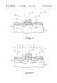
- FIG. 1illustrates a semiconductor wafer fragment indicated generally by reference numeral 10 .
- a semiconductor wafer fragmentindicated generally by reference numeral 10 .
- Suchis comprised of a bulk silicon substrate 12 and an overlying silicon dioxide layer 14 .
- the illustrationis simplified to focus on best-mode aspects of the invention, as opposed to showing possible and more typical substrate detail not particularly pertinent to the invention.
- a thin film transistor layer 16 of polycrystalline material, such as polysilicon or CdSe,is provided atop oxide layer 14 .
- An example method for providing layer 16would be to deposit an amorphous layer of silicon to a thickness between 25 and 50 nanometers, followed by solid phase crystallization at 600° C. in nitrogen for 24 hours. Such will result in a first average crystalline grain size throughout layer 16 of 0.1-0.2 microns.
- Layer 16is doped with an n-type conductivity enhancing impurity at a example dose of from 1 to 5 ⁇ 10 12 atoms/cm 2 to provide thin film layer 16 as n ⁇ doped. Thereafter, a thin layer 18 (preferably 250 Angstroms) of gate oxide is deposited, with an example thickness being from 10 to 50 nanometers. An ONO dielectric might preferably be substituted for SiO 2 of layer 18 .
- Thin film 16is then masked to define a masked portion 20 and an unmasked portion 22 .
- Masking in this exampleis most preferably conducted by deposition of an n+ doped polysilicon layer to a thickness of 200-300 nanometers, followed by subsequent patterning of such layer to produce a TFT gate 24 . Accordingly, this example principally addresses formation of a top gated thin film transistor.
- Masked portion 20comprises a thin film channel region 26 in polysilicon thin film 16 .
- Unmasked portion 22will comprise thin film source and drain regions within film 16 .
- Such unmasked portions 22also comprise a thin film drain offset region 28 (to be further defined subsequently) and an adjacent channel region 26 .
- the grain structure of polysilicon layer 16is uniform, having the first stated average crystalline grain size.
- an amorphizing silicon implantis conducted into unmasked portions 22 of thin film 16 to transform such unmasked polysilicon portion into amorphous silicon regions 30 .
- Alternate polycrystalline materialsmight be utilized, with the amorphizing silicon implant rendering such material into an amorphous phase.
- Suchcan be provided by a silicon atom implant dose of from 1 ⁇ 10 14 -1 ⁇ 10 15 atoms/cm 2 . Most preferred is a silicon atom implant of 3 ⁇ 10 14 atoms/cm 2 .
- Substrate 10is annealed to convert the amorphous silicon (or other amorphous material) back into polysilicon, with the converted polysilicon of regions 30 having a second average crystalline grain size which is greater than the first average crystalline grain size.
- Such re-crystallization annealingwill typically naturally occur to regions 30 of layer 16 throughout conventional semiconductor wafer processing which will ultimately subject the substrate to temperatures sufficiently high and sufficiently long to result in such recrystallization.
- a purposeful-dedicated recrystallization and anneal stepmight be conducted at, for example, 850° C. in a nitrogen atmosphere for thirty minutes to effect the recrystallization.
- the second average crystalline grain sizebecomes at least 50% to 200% greater than the first average crystalline grain size.
- An example first average crystalline grain sizeis approximately 0.1 microns, while an example preferred second average crystalline grain size is 0.2 microns.
- the FIG. 2 waferis then preferably subjected to a p-type dopant implant to provide regions 30 with a p ⁇ doping level.
- Example preferred doseswould include a BF 2 implant at 5 ⁇ 10 12 -5 ⁇ 10 13 cm ⁇ 2 .
- a layer of oxide, polysilicon or some other materialis deposited and subjected to an anisotropic spacer etch to produce the illustrated spacers 32 and 34 . Thereafter, substrate 10 is subjected to another p-type dopant impurity implant to produce a p+ drain region 36 and a p+ source region 38 . Such also completes definition of drain offset region 28 intermediate channel region 26 and drain region 36 . Such further defines a source offset region 40 which is operatively adjacent to and positioned between source region 38 and channel region 26 .
- thin film transistor layer 16comprises a source region 38 , a channel region 26 , a drain region 36 and two offset regions 28 and 40 .
- Drain offset region 28is operatively positioned between drain region 36 and channel region 26 .
- Channel region 26is substantially polycrystalline having a first average crystalline grain size.
- Drain offset region 28is likewise substantially polycrystalline, having a second average crystalline grain size which is larger than the first average crystalline grain size.
- An example preferred length range for each of drain offset regions 28 and source offset regions 40is from 0.1 micron to 0.5 micron.
- FIG. 4illustrates a simplified wafer 50 comprised of a bulk substrate 52 , oxide layer 53 , and overlying TFT gate 54 and opposingly adjacent insulating oxide regions 56 .
- a gate dielectric layer 58is provided atop regions 54 and 56 , followed by a thin film transistor polysilicon layer 60 provide with an n ⁇ doping.
- Gate 54thus defines a channel region 62 in thin film transistor layer 60 .
- a layer 64 of photoresistis deposited and patterned as shown preferably to expose only a drain offset region 66 of thin film layer 60 .
- photoresist layer 64masks all of thin film layer 60 but for drain offset region 66 .
- masking layer 64could be patterned to protect only the channel region.
- drain offset region 66is subjected to a p ⁇ level doping such as described above, followed by an amorphizing silicon implant to render region 66 amorphous.
- the amorphizing implantcould precede conductivity doping.
- Region 66will recrystallize upon appropriate elevated temperature exposure as described above to form polycrystalline silicon having a second average crystalline grain size which is greater than the first average crystalline grain size of the remainder portion of thin film layer 60 .
- photoresist layer 64has been removed and a subsequent implant masking layer 68 deposited and patterned as shown.
- Implant layer 68masks drain offset region 66 and channel region 62 , while exposing remaining regions of thin film layer 60 .
- exposed portions of thin film layer 60are subjected to a p+ implant to produce a drain region 70 and a source region 72 .
- a thin film transistor in accordance with the inventionis formed having a drain offset, but no source offset.
- Mask 68may then be removed, as shown in FIG. 7 . If masking material 68 comprises some other material such an insulative oxide, it might not be removed.
- the resultant productproduces a larger final average grain microstructure in the drain offset region as compared to the grain microstructure in the channel region.
- the current leakage typically trying to be prevented or minimized in SRAM or other transistorsis leakage occurring from the source through the channel region to the drain. Since leakage current is dependent upon trap concentration near the drain end of a thin film transistor, the above inventive approach will reduce leakage current as it reduces average trap concentration at the drain.
- the ON currentis also improved since it depends upon the grain size in both the channel region and the drain offset region. Smaller grains in the channel region are desirable for improved device-to-device uniformity. When channel grain size is large, some channel regions may have 1 grain boundary while others may have 4 grain boundaries (a four fold difference). However for channel regions with small grains, the number of grain boundaries will vary from 25 to 30. The difference between 25 and 30 is only a factor of 1.2 as opposed to 4.0. Accordingly, thin film transistors with more grains in the channel tend to have less device-to-device non-uniformity.
- the above technique for increasing crystalline grain sizewas by an amorphizing implant with subsequent crystallization, alternate methods might be utilized. For example, germanium implanting might be used.
- increasing grain size in the offset region as compared to the channel regionenhances overall conductivity of the offset region while minimizing current leakage. Accordingly, the drain offset region being an inherently higher conducting material than the channel region can be made longer to minimize undesired leakage current. Such should not appreciably adversely affect conductivity through the larger volume of material necessary for desired thin film transistor operation.
- thin film transistorsare constructed which only have a drain offset region, and no source offset region.
- FIG. 8illustrates an alternate preferred thin film transistor embodiment in accordance with the invention which comprises a gated offset region.
- the drain offset regionlies next to the gate sidewall.
- FIG. 8illustrates a wafer fragment 75 comprised of a bulk substrate 76 and overlying SiO 2 layer 78 .
- a thin film transistor polysilicon gate 80is provided atop layer 78 .
- a subsequent gate oxide dielectric layer 82(preferably ONO) is deposited atop polysilicon gate 80 .
- a thin film transistor layer 84is thereafter deposited. Such comprises a source region 86 , a channel region 88 , a drain offset region 90 , and a drain region 92 .
- the average crystalline grain size of drain offset region 90is provided to be greater than the average crystalline grain size of channel region 88 .
- the described constructionoverlaps offset region 90 with gate 80 . This effectively provides two transistors in series, where one is the main channel-transistor and the other is the an offset transistor. Overall transistor performance is improved by the effective gating of the offset region.
- the Poole-Frenkel and Thermionic Field Emission based leakage modelwas applied in evaluating the following process variations: gate oxide thickness, channel polysilicon thickness, offset doping concentration, and source/drain misalignment.
- the nominal device parameterswere 0.3 micron offset (FIG. 8, dimension 95 ); 250 Angstrom thick oxide dielectric layer 82 ; a 500 Angstrom thick channel polysilicon region 88 , 5.3 ⁇ 10 12 cm 2 (p) channel dose; and 5 ⁇ 10 12 cm 2 (BF 2 ) offset dose. It was found that when the gate oxide or channel polysilicon thickness is varied by plus or minus 20%, the leakage current variation is less than 3%.
- the leakage currentincreases dramatically. If the offset dose was decreased from 5 to 3 ⁇ 10 12 atoms/cm 2 , such that the net n-type doping concentration is higher, the leakage current increased by more than a factor of 10.
Landscapes
- Physics & Mathematics (AREA)
- Engineering & Computer Science (AREA)
- High Energy & Nuclear Physics (AREA)
- Condensed Matter Physics & Semiconductors (AREA)
- Toxicology (AREA)
- Health & Medical Sciences (AREA)
- General Physics & Mathematics (AREA)
- Manufacturing & Machinery (AREA)
- Computer Hardware Design (AREA)
- Microelectronics & Electronic Packaging (AREA)
- Power Engineering (AREA)
- Spectroscopy & Molecular Physics (AREA)
- Thin Film Transistor (AREA)
Abstract
Description
Claims (5)
Priority Applications (2)
| Application Number | Priority Date | Filing Date | Title |
|---|---|---|---|
| US09/442,340US6214652B1 (en) | 1994-10-24 | 1999-11-17 | Thin film transistors and method of forming thin film transistors |
| US09/742,149US6420219B2 (en) | 1994-10-24 | 2000-12-15 | Thin film transistors and method of forming thin film transistors |
Applications Claiming Priority (4)
| Application Number | Priority Date | Filing Date | Title |
|---|---|---|---|
| US32809694A | 1994-10-24 | 1994-10-24 | |
| US08/674,194US5904513A (en) | 1994-10-24 | 1996-07-01 | Method of forming thin film transistors |
| US09/124,939US6017782A (en) | 1994-10-24 | 1998-07-29 | Thin film transistor and method of forming thin film transistors |
| US09/442,340US6214652B1 (en) | 1994-10-24 | 1999-11-17 | Thin film transistors and method of forming thin film transistors |
Related Parent Applications (1)
| Application Number | Title | Priority Date | Filing Date |
|---|---|---|---|
| US09/124,939ContinuationUS6017782A (en) | 1994-10-24 | 1998-07-29 | Thin film transistor and method of forming thin film transistors |
Related Child Applications (1)
| Application Number | Title | Priority Date | Filing Date |
|---|---|---|---|
| US09/742,149ContinuationUS6420219B2 (en) | 1994-10-24 | 2000-12-15 | Thin film transistors and method of forming thin film transistors |
Publications (1)
| Publication Number | Publication Date |
|---|---|
| US6214652B1true US6214652B1 (en) | 2001-04-10 |
Family
ID=23279496
Family Applications (6)
| Application Number | Title | Priority Date | Filing Date |
|---|---|---|---|
| US08/484,979Expired - LifetimeUS5548132A (en) | 1994-10-24 | 1995-06-07 | Thin film transistor with large grain size DRW offset region and small grain size source and drain and channel regions |
| US08/674,194Expired - LifetimeUS5904513A (en) | 1994-10-24 | 1996-07-01 | Method of forming thin film transistors |
| US08/674,886Expired - LifetimeUS5936262A (en) | 1994-10-24 | 1996-07-02 | Thin film transistors |
| US09/124,939Expired - LifetimeUS6017782A (en) | 1994-10-24 | 1998-07-29 | Thin film transistor and method of forming thin film transistors |
| US09/442,340Expired - LifetimeUS6214652B1 (en) | 1994-10-24 | 1999-11-17 | Thin film transistors and method of forming thin film transistors |
| US09/742,149Expired - LifetimeUS6420219B2 (en) | 1994-10-24 | 2000-12-15 | Thin film transistors and method of forming thin film transistors |
Family Applications Before (4)
| Application Number | Title | Priority Date | Filing Date |
|---|---|---|---|
| US08/484,979Expired - LifetimeUS5548132A (en) | 1994-10-24 | 1995-06-07 | Thin film transistor with large grain size DRW offset region and small grain size source and drain and channel regions |
| US08/674,194Expired - LifetimeUS5904513A (en) | 1994-10-24 | 1996-07-01 | Method of forming thin film transistors |
| US08/674,886Expired - LifetimeUS5936262A (en) | 1994-10-24 | 1996-07-02 | Thin film transistors |
| US09/124,939Expired - LifetimeUS6017782A (en) | 1994-10-24 | 1998-07-29 | Thin film transistor and method of forming thin film transistors |
Family Applications After (1)
| Application Number | Title | Priority Date | Filing Date |
|---|---|---|---|
| US09/742,149Expired - LifetimeUS6420219B2 (en) | 1994-10-24 | 2000-12-15 | Thin film transistors and method of forming thin film transistors |
Country Status (1)
| Country | Link |
|---|---|
| US (6) | US5548132A (en) |
Cited By (4)
| Publication number | Priority date | Publication date | Assignee | Title |
|---|---|---|---|---|
| US6420219B2 (en)* | 1994-10-24 | 2002-07-16 | Micron Technology, Inc. | Thin film transistors and method of forming thin film transistors |
| US20030075746A1 (en)* | 2001-10-22 | 2003-04-24 | Mitsubishi Denki Kabushiki Kaisha | Semiconductor device for determining identification code and application thereof |
| US6563136B2 (en)* | 2000-08-10 | 2003-05-13 | Sony Corporation | Thin-film semiconductor device having a thin-film transistor for circuits that differs from a thin-film transistor for pixels |
| US6589828B2 (en)* | 1999-12-18 | 2003-07-08 | Hyundai Electronics Industries Co., Ltd. | Fabricating a thin film transistor having better punch through resistance and hot carrier effects |
Families Citing this family (38)
| Publication number | Priority date | Publication date | Assignee | Title |
|---|---|---|---|---|
| KR100205306B1 (en)* | 1995-12-26 | 1999-07-01 | 구본준 | Method of manufacturing thin film transistor |
| US5920085A (en)* | 1996-02-03 | 1999-07-06 | Samsung Electronics Co., Ltd. | Multiple floating gate field effect transistors and methods of operating same |
| KR0177785B1 (en)* | 1996-02-03 | 1999-03-20 | 김광호 | Transistor with Offset Structure and Manufacturing Method Thereof |
| EP0801427A3 (en)* | 1996-04-11 | 1999-05-06 | Matsushita Electric Industrial Co., Ltd. | Field effect transistor, semiconductor storage device, method of manufacturing the same and method of driving semiconductor storage device |
| US5602047A (en)* | 1996-06-13 | 1997-02-11 | Industrial Technology Research Institute | Process for polysilicon thin film transistors using backside irradiation and plasma doping |
| US5953596A (en) | 1996-12-19 | 1999-09-14 | Micron Technology, Inc. | Methods of forming thin film transistors |
| JP3424891B2 (en)* | 1996-12-27 | 2003-07-07 | 三洋電機株式会社 | Method of manufacturing thin film transistor and display device |
| US6329270B1 (en)* | 1997-03-07 | 2001-12-11 | Sharp Laboratories Of America, Inc. | Laser annealed microcrystalline film and method for same |
| KR100269600B1 (en)* | 1997-09-24 | 2000-10-16 | 김영환 | fabricatinf method of thin film transistor |
| KR20000009251A (en)* | 1998-07-22 | 2000-02-15 | 윤종용 | Gate electrode structure of semiconductor device and method for manufacturing the same |
| US6777210B1 (en)* | 1998-09-24 | 2004-08-17 | Ambion, Inc. | Method and reagents for inactivating ribonucleases RNase A, RNase I and RNase T1 |
| US6184112B1 (en)* | 1998-12-02 | 2001-02-06 | Advanced Micro Devices, Inc. | Method of forming a MOSFET transistor with a shallow abrupt retrograde dopant profile |
| US6306694B1 (en)* | 1999-03-12 | 2001-10-23 | Semiconductor Energy Laboratory Co., Ltd. | Process of fabricating a semiconductor device |
| US6512504B1 (en) | 1999-04-27 | 2003-01-28 | Semiconductor Energy Laborayory Co., Ltd. | Electronic device and electronic apparatus |
| US6200887B1 (en) | 2000-01-24 | 2001-03-13 | Chartered Semiconductor Manufacturing Ltd | Method to form a smooth gate polysilicon sidewall in the fabrication of integrated circuits |
| US6812493B2 (en)* | 2000-04-04 | 2004-11-02 | Matsushita Electric Industrial Co., Ltd. | Thin-film semiconductor element and method of producing same |
| US7416234B2 (en)* | 2002-02-08 | 2008-08-26 | Bequette Lawrence M | Vehicle sliding floor extension |
| US6794313B1 (en) | 2002-09-20 | 2004-09-21 | Taiwan Semiconductor Manufacturing Company, Ltd. | Oxidation process to improve polysilicon sidewall roughness |
| US6960794B2 (en)* | 2002-12-31 | 2005-11-01 | Matrix Semiconductor, Inc. | Formation of thin channels for TFT devices to ensure low variability of threshold voltages |
| JP4321111B2 (en)* | 2003-05-16 | 2009-08-26 | 日本電気株式会社 | OPTICAL MODULE, METHOD FOR RELEASE LOCK STATUS OF OPTICAL MODULE AND CAGE |
| DE10322588B4 (en)* | 2003-05-20 | 2006-10-05 | Infineon Technologies Ag | Method for producing a resistance layer |
| KR100640975B1 (en)* | 2005-12-29 | 2006-11-02 | 동부일렉트로닉스 주식회사 | Resistor Formation Method of Semiconductor Device |
| US20070194450A1 (en)* | 2006-02-21 | 2007-08-23 | Tyberg Christy S | BEOL compatible FET structure |
| KR100785038B1 (en)* | 2006-04-17 | 2007-12-12 | 삼성전자주식회사 | Amorphous ZnO based Thin Film Transistor |
| KR100810638B1 (en)* | 2006-12-06 | 2008-03-07 | 삼성에스디아이 주식회사 | Thin film transistor, manufacturing method thereof and organic light emitting display device having same |
| KR100810639B1 (en)* | 2006-12-06 | 2008-03-07 | 삼성에스디아이 주식회사 | Thin film transistor, manufacturing method thereof and organic light emitting display device having same |
| KR101509663B1 (en) | 2007-02-16 | 2015-04-06 | 삼성전자주식회사 | Method of forming oxide semiconductor layer and method of manufacturing semiconductor device using the same |
| KR100875730B1 (en)* | 2007-03-05 | 2008-12-24 | 삼성전자주식회사 | Semiconductor device and manufacturing method thereof |
| KR20080088284A (en)* | 2007-03-29 | 2008-10-02 | 삼성전자주식회사 | Flash memory devices |
| KR101334181B1 (en)* | 2007-04-20 | 2013-11-28 | 삼성전자주식회사 | Thin Film Transistor having selectively crystallized channel layer and method of manufacturing the same |
| JP2010530634A (en) | 2007-06-19 | 2010-09-09 | サムスン エレクトロニクス カンパニー リミテッド | Oxide semiconductor and thin film transistor including the same |
| US7935964B2 (en)* | 2007-06-19 | 2011-05-03 | Samsung Electronics Co., Ltd. | Oxide semiconductors and thin film transistors comprising the same |
| KR101015847B1 (en)* | 2008-01-18 | 2011-02-23 | 삼성모바일디스플레이주식회사 | Thin film transistor, manufacturing method thereof and organic light emitting display device having same |
| KR101496148B1 (en)* | 2008-05-15 | 2015-02-27 | 삼성전자주식회사 | Semiconductor device and manufacturing method thereof |
| KR101468591B1 (en)* | 2008-05-29 | 2014-12-04 | 삼성전자주식회사 | Oxide semiconductor and thin film transistor comprising the same |
| US9230991B2 (en)* | 2014-04-16 | 2016-01-05 | Stmicroelectronics, Inc. | Method to co-integrate oppositely strained semiconductor devices on a same substrate |
| CN105304500B (en)* | 2015-10-26 | 2018-01-30 | 深圳市华星光电技术有限公司 | N-type TFT preparation method |
| CN105742294B (en)* | 2016-03-23 | 2019-01-15 | 深圳市华星光电技术有限公司 | The production method of TFT substrate and TFT substrate obtained |
Citations (32)
| Publication number | Priority date | Publication date | Assignee | Title |
|---|---|---|---|---|
| JPS5856467A (en) | 1981-09-30 | 1983-04-04 | Toshiba Corp | Manufacture of semiconductor device |
| US4385937A (en) | 1980-05-20 | 1983-05-31 | Tokyo Shibaura Denki Kabushiki Kaisha | Regrowing selectively formed ion amorphosized regions by thermal gradient |
| US4420870A (en) | 1980-10-09 | 1983-12-20 | Tokyo Shibaura Denki Kabushiki Kaisha | Method of controlling channel length by implanting through polycrystalline and single crystalline regions followed by diffusion anneal |
| US4498224A (en) | 1982-12-23 | 1985-02-12 | Tokyo Shibaura Denki Kabushiki Kaisha | Method of manufacturing a MOSFET using accelerated ions to form an amorphous region |
| US4528480A (en) | 1981-12-28 | 1985-07-09 | Nippon Telegraph & Telephone | AC Drive type electroluminescent display device |
| JPS6276772A (en) | 1985-09-30 | 1987-04-08 | Sony Corp | Manufacturing method of field effect transistor |
| JPS6411369A (en) | 1987-07-03 | 1989-01-13 | Nec Corp | Manufacture of polycrystalline silicon thin film transistor |
| JPS6450569A (en) | 1987-08-21 | 1989-02-27 | Nec Corp | Manufacture of polycrystalline silicon thin film transistor |
| JPH01158775A (en) | 1987-12-16 | 1989-06-21 | Seiko Epson Corp | Manufacturing method of thin film transistor |
| JPH01251668A (en) | 1988-03-30 | 1989-10-06 | Nec Corp | Manufacture of field effect transistor |
| JPH03104210A (en) | 1989-09-19 | 1991-05-01 | Fujitsu Ltd | Manufacture of semiconductor device |
| US5112764A (en) | 1990-09-04 | 1992-05-12 | North American Philips Corporation | Method for the fabrication of low leakage polysilicon thin film transistors |
| JPH04152639A (en) | 1990-10-17 | 1992-05-26 | Seiko Epson Corp | Manufacturing method of semiconductor device |
| JPH04162432A (en) | 1990-10-24 | 1992-06-05 | Nippon Sheet Glass Co Ltd | Manufacture of semiconductor device |
| JPH04306843A (en) | 1991-04-03 | 1992-10-29 | Mitsubishi Electric Corp | Semiconductor device and its manufacturing method |
| US5198379A (en) | 1990-04-27 | 1993-03-30 | Sharp Kabushiki Kaisha | Method of making a MOS thin film transistor with self-aligned asymmetrical structure |
| US5208476A (en) | 1990-06-08 | 1993-05-04 | Seiko Epson Corporation | Low leakage current offset-gate thin film transistor structure |
| JPH05152329A (en) | 1991-11-29 | 1993-06-18 | Casio Comput Co Ltd | Method of manufacturing thin film transistor |
| US5266507A (en) | 1992-05-18 | 1993-11-30 | Industrial Technology Research Institute | Method of fabricating an offset dual gate thin film field effect transistor |
| US5286663A (en) | 1992-01-29 | 1994-02-15 | Micron Technology, Inc. | Methods for producing thin film transistor having a diode shunt |
| US5292675A (en) | 1991-12-24 | 1994-03-08 | Semiconductor Energy Laboratory Co., Ltd. | Method for forming a MOS transistor and structure thereof |
| JPH06112223A (en) | 1992-09-29 | 1994-04-22 | Seiko Epson Corp | Method of manufacturing thin film transistor |
| US5308998A (en) | 1991-08-26 | 1994-05-03 | Semiconductor Energy Laboratory Co., Ltd. | Insulated gate field effect semiconductor devices having a LDD region and an anodic oxide film of a gate electrode |
| JPH06163580A (en) | 1992-11-20 | 1994-06-10 | Sharp Corp | Manufacture of thin-film transistor |
| US5323042A (en) | 1991-11-25 | 1994-06-21 | Casio Computer Co., Ltd. | Active matrix liquid crystal display having a peripheral driving circuit element |
| JPH06232160A (en) | 1993-02-01 | 1994-08-19 | Fuji Xerox Co Ltd | Manufacture of thin film transistor |
| US5344790A (en) | 1993-08-31 | 1994-09-06 | Sgs-Thomson Microelectronics, Inc. | Making integrated circuit transistor having drain junction offset |
| US5412493A (en) | 1992-09-25 | 1995-05-02 | Sony Corporation | Liquid crystal display device having LDD structure type thin film transistors connected in series |
| US5420055A (en) | 1992-01-22 | 1995-05-30 | Kopin Corporation | Reduction of parasitic effects in floating body MOSFETs |
| US5457058A (en) | 1989-10-09 | 1995-10-10 | Canon Kabushiki Kaisha | Crystal growth method |
| US5904513A (en)* | 1994-10-24 | 1999-05-18 | Micron Technology, Inc. | Method of forming thin film transistors |
| JP3104210B2 (en) | 1991-03-29 | 2000-10-30 | ヤマハ発動機株式会社 | Unmanned traveling vehicle |
Family Cites Families (2)
| Publication number | Priority date | Publication date | Assignee | Title |
|---|---|---|---|---|
| US4451445A (en)* | 1982-08-31 | 1984-05-29 | General Electric Company | Method for controlled hydrogen charging of metals |
| US4728507A (en)* | 1987-01-09 | 1988-03-01 | Westinghouse Electric Corp. | Preparation of reactive metal hydrides |
- 1995
- 1995-06-07USUS08/484,979patent/US5548132A/ennot_activeExpired - Lifetime
- 1996
- 1996-07-01USUS08/674,194patent/US5904513A/ennot_activeExpired - Lifetime
- 1996-07-02USUS08/674,886patent/US5936262A/ennot_activeExpired - Lifetime
- 1998
- 1998-07-29USUS09/124,939patent/US6017782A/ennot_activeExpired - Lifetime
- 1999
- 1999-11-17USUS09/442,340patent/US6214652B1/ennot_activeExpired - Lifetime
- 2000
- 2000-12-15USUS09/742,149patent/US6420219B2/ennot_activeExpired - Lifetime
Patent Citations (32)
| Publication number | Priority date | Publication date | Assignee | Title |
|---|---|---|---|---|
| US4385937A (en) | 1980-05-20 | 1983-05-31 | Tokyo Shibaura Denki Kabushiki Kaisha | Regrowing selectively formed ion amorphosized regions by thermal gradient |
| US4420870A (en) | 1980-10-09 | 1983-12-20 | Tokyo Shibaura Denki Kabushiki Kaisha | Method of controlling channel length by implanting through polycrystalline and single crystalline regions followed by diffusion anneal |
| JPS5856467A (en) | 1981-09-30 | 1983-04-04 | Toshiba Corp | Manufacture of semiconductor device |
| US4528480A (en) | 1981-12-28 | 1985-07-09 | Nippon Telegraph & Telephone | AC Drive type electroluminescent display device |
| US4498224A (en) | 1982-12-23 | 1985-02-12 | Tokyo Shibaura Denki Kabushiki Kaisha | Method of manufacturing a MOSFET using accelerated ions to form an amorphous region |
| JPS6276772A (en) | 1985-09-30 | 1987-04-08 | Sony Corp | Manufacturing method of field effect transistor |
| JPS6411369A (en) | 1987-07-03 | 1989-01-13 | Nec Corp | Manufacture of polycrystalline silicon thin film transistor |
| JPS6450569A (en) | 1987-08-21 | 1989-02-27 | Nec Corp | Manufacture of polycrystalline silicon thin film transistor |
| JPH01158775A (en) | 1987-12-16 | 1989-06-21 | Seiko Epson Corp | Manufacturing method of thin film transistor |
| JPH01251668A (en) | 1988-03-30 | 1989-10-06 | Nec Corp | Manufacture of field effect transistor |
| JPH03104210A (en) | 1989-09-19 | 1991-05-01 | Fujitsu Ltd | Manufacture of semiconductor device |
| US5457058A (en) | 1989-10-09 | 1995-10-10 | Canon Kabushiki Kaisha | Crystal growth method |
| US5198379A (en) | 1990-04-27 | 1993-03-30 | Sharp Kabushiki Kaisha | Method of making a MOS thin film transistor with self-aligned asymmetrical structure |
| US5208476A (en) | 1990-06-08 | 1993-05-04 | Seiko Epson Corporation | Low leakage current offset-gate thin film transistor structure |
| US5112764A (en) | 1990-09-04 | 1992-05-12 | North American Philips Corporation | Method for the fabrication of low leakage polysilicon thin film transistors |
| JPH04152639A (en) | 1990-10-17 | 1992-05-26 | Seiko Epson Corp | Manufacturing method of semiconductor device |
| JPH04162432A (en) | 1990-10-24 | 1992-06-05 | Nippon Sheet Glass Co Ltd | Manufacture of semiconductor device |
| JP3104210B2 (en) | 1991-03-29 | 2000-10-30 | ヤマハ発動機株式会社 | Unmanned traveling vehicle |
| JPH04306843A (en) | 1991-04-03 | 1992-10-29 | Mitsubishi Electric Corp | Semiconductor device and its manufacturing method |
| US5308998A (en) | 1991-08-26 | 1994-05-03 | Semiconductor Energy Laboratory Co., Ltd. | Insulated gate field effect semiconductor devices having a LDD region and an anodic oxide film of a gate electrode |
| US5323042A (en) | 1991-11-25 | 1994-06-21 | Casio Computer Co., Ltd. | Active matrix liquid crystal display having a peripheral driving circuit element |
| JPH05152329A (en) | 1991-11-29 | 1993-06-18 | Casio Comput Co Ltd | Method of manufacturing thin film transistor |
| US5292675A (en) | 1991-12-24 | 1994-03-08 | Semiconductor Energy Laboratory Co., Ltd. | Method for forming a MOS transistor and structure thereof |
| US5420055A (en) | 1992-01-22 | 1995-05-30 | Kopin Corporation | Reduction of parasitic effects in floating body MOSFETs |
| US5286663A (en) | 1992-01-29 | 1994-02-15 | Micron Technology, Inc. | Methods for producing thin film transistor having a diode shunt |
| US5266507A (en) | 1992-05-18 | 1993-11-30 | Industrial Technology Research Institute | Method of fabricating an offset dual gate thin film field effect transistor |
| US5412493A (en) | 1992-09-25 | 1995-05-02 | Sony Corporation | Liquid crystal display device having LDD structure type thin film transistors connected in series |
| JPH06112223A (en) | 1992-09-29 | 1994-04-22 | Seiko Epson Corp | Method of manufacturing thin film transistor |
| JPH06163580A (en) | 1992-11-20 | 1994-06-10 | Sharp Corp | Manufacture of thin-film transistor |
| JPH06232160A (en) | 1993-02-01 | 1994-08-19 | Fuji Xerox Co Ltd | Manufacture of thin film transistor |
| US5344790A (en) | 1993-08-31 | 1994-09-06 | Sgs-Thomson Microelectronics, Inc. | Making integrated circuit transistor having drain junction offset |
| US5904513A (en)* | 1994-10-24 | 1999-05-18 | Micron Technology, Inc. | Method of forming thin film transistors |
Non-Patent Citations (12)
| Title |
|---|
| Batra et al., "Development of Polysilicon TFT's for 16 Mb SRAMs and Beyond", SB Sep. 28, 1994, Jun. 21, 1993. |
| Batra et al., "Development of Polysilicon TFT's for 16Mb SRAMs and Beyond", Sep. 28, 1994, 2 pages. |
| Batra, Shubneesh, "Development of Drain-Offset (DO) TFT Technology for High Density SRAMs", Oct. 9, 1994. |
| Batra, Shubneesh, Development of Drain-Offset (DO) TFT Technology for High Density SRAMs, Oct. 9, 1994, 2 pages. |
| Colinge et al., "Field Effect in Large Grain Polycrystalline Silicon", IEEE Transactions on Electron Devices, vol. ED-30, No. 3, Mar. 1983, pp. 197-201. |
| Hashimoto et al., "Thin Film Effects of Double-Gate Polysilicon MOSFET", Ext. Abstracts of the 22nd Conf. of S.S. Devices and Materials, 1990, pp. 393-396. |
| Hasimoto et al., Thin Film Effects of Double-Gate Polysilicon MOSFET, Ext. Abstracts of the 22nd Conf. of S.S. Devices and Materials, 1990, pp. 393-396. |
| Hayden et al., A High-Performance Quadruple Well, Quadruple Poly BiCMOS Process For Fast 16Mb SRAMs, IEEE, IEDM 92/819, pp. 819-822, 1992. |
| Jung et al., "A Leakage Current Model for Sub-Micron Drain-Offset Polysilicon TFT's", Oct. 9, 1994, 4 pages. |
| Tanaka et al., "Field-Induction Drain (FID) Poly-Si TFTs With High On/Off Current Ratio", Extended Abstracts of the 22nd Conf. on S.S. Devices and Materials, 1990, pp. 1011, 1014. |
| Webster's Ninth New College Dictionary, 1990, p. 1198. |
| Wolf, S., "Silicon Processing For The VLSI Era", vol. II, pp. 354-361 and 436-439. |
Cited By (4)
| Publication number | Priority date | Publication date | Assignee | Title |
|---|---|---|---|---|
| US6420219B2 (en)* | 1994-10-24 | 2002-07-16 | Micron Technology, Inc. | Thin film transistors and method of forming thin film transistors |
| US6589828B2 (en)* | 1999-12-18 | 2003-07-08 | Hyundai Electronics Industries Co., Ltd. | Fabricating a thin film transistor having better punch through resistance and hot carrier effects |
| US6563136B2 (en)* | 2000-08-10 | 2003-05-13 | Sony Corporation | Thin-film semiconductor device having a thin-film transistor for circuits that differs from a thin-film transistor for pixels |
| US20030075746A1 (en)* | 2001-10-22 | 2003-04-24 | Mitsubishi Denki Kabushiki Kaisha | Semiconductor device for determining identification code and application thereof |
Also Published As
| Publication number | Publication date |
|---|---|
| US6420219B2 (en) | 2002-07-16 |
| US6017782A (en) | 2000-01-25 |
| US5548132A (en) | 1996-08-20 |
| US20010000756A1 (en) | 2001-05-03 |
| US5904513A (en) | 1999-05-18 |
| US5936262A (en) | 1999-08-10 |
Similar Documents
| Publication | Publication Date | Title |
|---|---|---|
| US6214652B1 (en) | Thin film transistors and method of forming thin film transistors | |
| US5198379A (en) | Method of making a MOS thin film transistor with self-aligned asymmetrical structure | |
| US6569715B1 (en) | Large grain single crystal vertical thin film polysilicon mosfets | |
| US7452760B2 (en) | Thin film transistors and semiconductor constructions | |
| US5385854A (en) | Method of forming a self-aligned low density drain inverted thin film transistor | |
| US5849612A (en) | MOS poly-si thin film transistor with a flattened channel interface and method of producing same | |
| JPS63255968A (en) | Method for manufacturing field effect transistors | |
| US5403761A (en) | Method of fabricating a thin film transistor | |
| EP0457434B1 (en) | MOS thin film transistor having a drain offset region | |
| US5821584A (en) | Thin film transistors comprising drain offset regions | |
| US6077732A (en) | Method of forming a thin film transistor | |
| US5459088A (en) | Method for making a thin film transistor | |
| JPH1056147A (en) | Semiconductor device and manufacturing method thereof | |
| JP2787546B2 (en) | Method for manufacturing thin film transistor | |
| JPH0669094B2 (en) | Field effect transistor | |
| US6589828B2 (en) | Fabricating a thin film transistor having better punch through resistance and hot carrier effects | |
| KR100476377B1 (en) | Thin Film Transistor Manufacturing Method | |
| KR0136532B1 (en) | Method of manufacturing thin film transistor | |
| US5943579A (en) | Method for forming a diffusion region in a semiconductor device | |
| JP2746500B2 (en) | MOS transistor | |
| KR960015933B1 (en) | Semiconductor thin film transistor (TFT) manufacturing method | |
| KR100260484B1 (en) | Thi film transistor and making method thereof | |
| KR0177386B1 (en) | Method of manufacturing thin film transistor | |
| JPS63255966A (en) | Field effect transistor | |
| JPH05129334A (en) | Thin film transistor and its manufacture |
Legal Events
| Date | Code | Title | Description |
|---|---|---|---|
| FEPP | Fee payment procedure | Free format text:PAYOR NUMBER ASSIGNED (ORIGINAL EVENT CODE: ASPN); ENTITY STATUS OF PATENT OWNER: LARGE ENTITY | |
| STCF | Information on status: patent grant | Free format text:PATENTED CASE | |
| CC | Certificate of correction | ||
| FPAY | Fee payment | Year of fee payment:4 | |
| FPAY | Fee payment | Year of fee payment:8 | |
| FPAY | Fee payment | Year of fee payment:12 | |
| AS | Assignment | Owner name:U.S. BANK NATIONAL ASSOCIATION, AS COLLATERAL AGENT, CALIFORNIA Free format text:SECURITY INTEREST;ASSIGNOR:MICRON TECHNOLOGY, INC.;REEL/FRAME:038669/0001 Effective date:20160426 Owner name:U.S. BANK NATIONAL ASSOCIATION, AS COLLATERAL AGEN Free format text:SECURITY INTEREST;ASSIGNOR:MICRON TECHNOLOGY, INC.;REEL/FRAME:038669/0001 Effective date:20160426 | |
| AS | Assignment | Owner name:MORGAN STANLEY SENIOR FUNDING, INC., AS COLLATERAL AGENT, MARYLAND Free format text:PATENT SECURITY AGREEMENT;ASSIGNOR:MICRON TECHNOLOGY, INC.;REEL/FRAME:038954/0001 Effective date:20160426 Owner name:MORGAN STANLEY SENIOR FUNDING, INC., AS COLLATERAL Free format text:PATENT SECURITY AGREEMENT;ASSIGNOR:MICRON TECHNOLOGY, INC.;REEL/FRAME:038954/0001 Effective date:20160426 | |
| AS | Assignment | Owner name:U.S. BANK NATIONAL ASSOCIATION, AS COLLATERAL AGENT, CALIFORNIA Free format text:CORRECTIVE ASSIGNMENT TO CORRECT THE REPLACE ERRONEOUSLY FILED PATENT #7358718 WITH THE CORRECT PATENT #7358178 PREVIOUSLY RECORDED ON REEL 038669 FRAME 0001. ASSIGNOR(S) HEREBY CONFIRMS THE SECURITY INTEREST;ASSIGNOR:MICRON TECHNOLOGY, INC.;REEL/FRAME:043079/0001 Effective date:20160426 Owner name:U.S. BANK NATIONAL ASSOCIATION, AS COLLATERAL AGEN Free format text:CORRECTIVE ASSIGNMENT TO CORRECT THE REPLACE ERRONEOUSLY FILED PATENT #7358718 WITH THE CORRECT PATENT #7358178 PREVIOUSLY RECORDED ON REEL 038669 FRAME 0001. ASSIGNOR(S) HEREBY CONFIRMS THE SECURITY INTEREST;ASSIGNOR:MICRON TECHNOLOGY, INC.;REEL/FRAME:043079/0001 Effective date:20160426 | |
| AS | Assignment | Owner name:MICRON TECHNOLOGY, INC., IDAHO Free format text:RELEASE BY SECURED PARTY;ASSIGNOR:U.S. BANK NATIONAL ASSOCIATION, AS COLLATERAL AGENT;REEL/FRAME:047243/0001 Effective date:20180629 | |
| AS | Assignment | Owner name:MICRON TECHNOLOGY, INC., IDAHO Free format text:RELEASE BY SECURED PARTY;ASSIGNOR:MORGAN STANLEY SENIOR FUNDING, INC., AS COLLATERAL AGENT;REEL/FRAME:050937/0001 Effective date:20190731 |