US6212246B1 - Symbol-quality evaluation in a digital communications receiver - Google Patents
Symbol-quality evaluation in a digital communications receiverDownload PDFInfo
- Publication number
- US6212246B1 US6212246B1US09/078,225US7822598AUS6212246B1US 6212246 B1US6212246 B1US 6212246B1US 7822598 AUS7822598 AUS 7822598AUS 6212246 B1US6212246 B1US 6212246B1
- Authority
- US
- United States
- Prior art keywords
- symbol
- signal
- quality
- magnitude
- symbols
- Prior art date
- Legal status (The legal status is an assumption and is not a legal conclusion. Google has not performed a legal analysis and makes no representation as to the accuracy of the status listed.)
- Expired - Lifetime
Links
- 238000004891communicationMethods0.000titleclaimsabstractdescription25
- 238000013441quality evaluationMethods0.000title1
- 238000000034methodMethods0.000claimsabstractdescription22
- 230000007704transitionEffects0.000claimsabstractdescription20
- 238000011084recoveryMethods0.000claimsdescription38
- 230000004044responseEffects0.000claimsdescription6
- 238000012360testing methodMethods0.000abstractdescription9
- 230000007423decreaseEffects0.000abstractdescription3
- 230000001934delayEffects0.000abstractdescription2
- 238000001228spectrumMethods0.000description15
- 230000007480spreadingEffects0.000description9
- 238000012545processingMethods0.000description6
- 238000010586diagramMethods0.000description5
- 108091081062Repeated sequence (DNA)Proteins0.000description4
- 230000008901benefitEffects0.000description4
- 238000013461designMethods0.000description4
- 230000006870functionEffects0.000description4
- 238000012986modificationMethods0.000description4
- 230000004048modificationEffects0.000description4
- 239000013598vectorSubstances0.000description4
- 230000005540biological transmissionEffects0.000description3
- 230000010363phase shiftEffects0.000description3
- 238000005070samplingMethods0.000description3
- 238000004364calculation methodMethods0.000description2
- 230000001427coherent effectEffects0.000description2
- 238000001914filtrationMethods0.000description2
- 238000004519manufacturing processMethods0.000description2
- 230000000737periodic effectEffects0.000description2
- 230000008569processEffects0.000description2
- 230000001360synchronised effectEffects0.000description2
- 238000012795verificationMethods0.000description2
- 239000000654additiveSubstances0.000description1
- 230000000996additive effectEffects0.000description1
- 230000003321amplificationEffects0.000description1
- 238000004458analytical methodMethods0.000description1
- 230000015556catabolic processEffects0.000description1
- 230000010267cellular communicationEffects0.000description1
- 230000008859changeEffects0.000description1
- 238000006243chemical reactionMethods0.000description1
- 238000006731degradation reactionMethods0.000description1
- 238000001514detection methodMethods0.000description1
- 230000000694effectsEffects0.000description1
- 238000011156evaluationMethods0.000description1
- 238000012423maintenanceMethods0.000description1
- 238000012544monitoring processMethods0.000description1
- 238000003199nucleic acid amplification methodMethods0.000description1
- 230000010355oscillationEffects0.000description1
- 230000001902propagating effectEffects0.000description1
- 238000013139quantizationMethods0.000description1
- 238000000638solvent extractionMethods0.000description1
- 230000003595spectral effectEffects0.000description1
- 238000006467substitution reactionMethods0.000description1
- 230000000153supplemental effectEffects0.000description1
Images


Classifications
- H—ELECTRICITY
- H04—ELECTRIC COMMUNICATION TECHNIQUE
- H04L—TRANSMISSION OF DIGITAL INFORMATION, e.g. TELEGRAPHIC COMMUNICATION
- H04L1/00—Arrangements for detecting or preventing errors in the information received
- H04L1/24—Testing correct operation
- H—ELECTRICITY
- H04—ELECTRIC COMMUNICATION TECHNIQUE
- H04L—TRANSMISSION OF DIGITAL INFORMATION, e.g. TELEGRAPHIC COMMUNICATION
- H04L7/00—Arrangements for synchronising receiver with transmitter
- H04L7/0054—Detection of the synchronisation error by features other than the received signal transition
- H—ELECTRICITY
- H04—ELECTRIC COMMUNICATION TECHNIQUE
- H04L—TRANSMISSION OF DIGITAL INFORMATION, e.g. TELEGRAPHIC COMMUNICATION
- H04L7/00—Arrangements for synchronising receiver with transmitter
- H04L7/02—Speed or phase control by the received code signals, the signals containing no special synchronisation information
- H04L7/033—Speed or phase control by the received code signals, the signals containing no special synchronisation information using the transitions of the received signal to control the phase of the synchronising-signal-generating means, e.g. using a phase-locked loop
- H04L7/0334—Processing of samples having at least three levels, e.g. soft decisions
Definitions
- the inventionrelates to electronic communication and, more particularly, to symbol-clock recovery in a digital receiver.
- Electronic communicationis generally accomplished through a carrier wave that is modulated to bear data from a transmitting unit to a receiving unit.
- the transmission of digital datainvolves several steps, including partitioning the data into a sequence of symbols, modulating the carrier wave with the sequence of symbols to produce the transmitted signal, and propagating the transmitted signal through a communication channel.
- the received signalis received by the receiver which demodulates it to extract the received symbols.
- the receiverquantizes the symbols to reproduce the transmitted digital data.
- An important component of the receiveris a symbol clock used in demodulating the received signal and quantizing the symbols.
- the symbol clockgenerates a signal at the symbol rate of the received signal.
- the symbol clockindicates the boundaries between symbols in the received signal, and is an important input to various elements in the receiver such as matched filters, differential decoders, and slicers. If the symbol clock signal deviates from the correct timing of the symbol boundaries, the function of all of these components is degraded, increasing the receiver's error rate. It is therefore helpful to have a system for evaluating the symbol clock and detecting drifts in its phase from the timing of the symbol sequence.
- Prior-art symbol-timing recovery circuitsuse open-loop synchronizers, which use no feedback to the symbol clock, and closed-loop synchronizers, which test small shifts in the symbol timing for improved symbol synchronization and adjust the symbol clock accordingly.
- the closed-loop synchronizerssuch as early/late-gate loops and tau-dither loops, generate error signals indicative of the phase offset between the symbol boundaries and the symbol clock.
- the early/late-gate loopsdepend on symbol transitions to generate the error signals. Hence, they are prone to drifting from the correct symbol timing when the received signal contains a run of repeated symbols. This problem is reduced by having better-balanced integrators or by using a tau-dither loop, but both of these measures add significantly to the complexity of the synchronizers.
- Such a systemcould also be used to configure a receiver with an appropriate timing for its symbol clock. If a receiver derives its symbol clock from another clock that has the same frequency but has a phase offset from the symbol transitions, then this system for evaluating the symbol clock would provide a simple means for measuring the phase offset at the end of the manufacturing process. The receiver can then be configured to use the measured value as an initial estimate of the offset during future operation.
- One embodiment of the present inventioncontemplates a system and method for evaluating the quality of symbols in a communications receiver and for adjusting a symbol clock in the receiver so that the symbol quality is maximized.
- the inventionpresents a symbol quality detector, comprised in the receiver, that evaluates symbols which have been received by the receiver and detected in a matched filter.
- the constellation points ⁇ X n ⁇can be described in a 2-dimensional Cartesian plane as:
- ⁇ X n⁇ (0,A), (A,0), ( ⁇ A,0), (0, ⁇ A) ⁇ .
- the projection of a given symbol X n along the ordinate Iis a vector labeled i
- the projection along the abscissa Qis a vector labeled q.
- the i and q vectorsform a 2-dimensional orthonormal vector basis when the amplitude A is appropriately normalized.
- the projections of the received symbols on the ordinate and abscissaare referred to as the I and Q components of the received symbol, respectively, or more simply, as I and Q.
- the symbol-quality detectorcomprises inputs that receive I and Q, and a logic block that generates the symbol-quality signal by constructing the quantity
- the symbol-quality detectorcomprises a latch that permits updates of the symbol-quality signal only during receive cycles, in which the receiver receives data.
- the inventionfurther contemplates an arrangement of elements in the logic-block of the symbol-quality detector.
- the logic blockcomprises magnitude detectors that calculate the magnitudes of the I and Q components, an adder that adds the magnitude of the I component with the compliment of the magnitude Q component, thereby generating the difference
- the present inventioncomprises a digital communications receiver that uses a symbol-quality detector to evaluate its symbol clock. Since a poor synchronization will cause the detected symbols to deviate from the expected constellation points, the symbol-quality signal is used in the receiver to measure the synchronization of the symbol clock with the symbol transitions in the received signal. This measure is preferably used to shift a phase of the symbol clock to refine its synchronization with the received symbols.
- a second embodiment of the present inventioncontemplates a method for configuring the receiver with an IF delay value that indicates the timing of symbol transitions in a received signal processed by the receiver.
- the receiverrecovers from the received signal a timing that has the same period as the symbol period, but which is out of phase with the received symbols.
- the methoddetermines an optimal delay value by which the symbol clock should be shifted from the recovered timing so that the symbol clock is in phase with the symbol transitions.
- the methoduses the symbol-quality signal to evaluate test delays and to successively refine them until the optimal delay value is found.
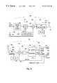
- FIG. 1shows a representative direct sequence spread spectrum transceiver, a block diagram of the primary modules in the transceiver, and a schematic of the transceiver;
- FIG. 2is a block diagram of the passband DQPSK decoder from FIG. 1;
- FIG. 3is a block diagram of the symbol-quality detector from FIG. 2;
- FIG. 4illustrates a test-bench configuration for configuring the transceiver with a pre-programmed IF delay
- FIG. 5is a flowchart for configuring the transceiver with the pre-programmed IF delay.
- FIG. 1DQPSK Spread Spectrum Transceiver
- the present inventionis comprised in the receiver of a digital communication system.
- Digital receiversare ubiquitous in cordless, mobile, and cellular communications systems, as well as in transmission-line and fiber-optic information networks.
- the receiverreceives a received signal carrying transmitted data and demodulates it to extract the received symbols.
- the receiverthen quantizes the symbols to reproduce the transmitted digital data.
- the present inventioncomprises a system and method for generating a symbol-quality signal to monitor the symbol clock used in demodulating the received signal.
- the inventionis comprised in a cordless telephone system that uses direct sequence spread spectrum techniques and differential quadriphase shift keying (DQPSK) to convey data between transceivers.
- DQPSKdifferential quadriphase shift keying
- FIG. 1 ais a representative view of a time-division duplexing (TDD) transceiver 10 that communicates with a remote transceiver (not shown) through a direct sequence spread spectrum signal.
- TDDtime-division duplexing
- FIG. 1 bA block diagram of the transceiver's signal-processing components is shown in FIG. 1 b . The components and the associated signals in the transceiver are further described in FIG. 1 c .
- the inventionis preferably comprised in such a transceiver 10 , which has a local transmitter 100 that transmits a radio frequency (RF) transmit signal 110 to the remote transceiver, and a local receiver 150 that receives an RF received signal 160 from the remote transceiver.
- RFradio frequency
- a DQPSK line coder 106 in the transmitter 100receives a stream of transmitted data 102 and encodes it into a complex baseband transmit signal 107 that comprises a series of information symbols each with a duration T.
- the symbol period Tis 15.625 ⁇ s, implying a symbol rate of 64 kS/sec.
- the baseband transmit signal 107is upconverted to an intermediate-frequency (IF) transmit signal 108 in a complex IF mixer 125 .
- a spreading mixer 135receives the transmit signal 108 and multiplies it by a pseudo-random noise (PN) sequence that serves as a spreading code. The timing of this PN sequence is controlled by a transmitter PN clock 131 .
- PNpseudo-random noise
- the multiplication by the transmitter PN sequencespreads the frequency spectrum of the narrowband transmit signal 108 .
- the resulting wideband IF transmit signal 109is provided to a RF modulator 146 that multiplies it with a radio-frequency tone to generate the RF transmit signal 110 . In one embodiment of the invention, this frequency is in the vicinity of 900 MHz.
- the RF transmit signal 110is then sent through a transmitting antenna 148 to the remote transceiver (not shown).
- the receiver 150 in the transceiver 10comprises components that reverse the processing steps of those in the transmitter 100 .
- a receiving antenna 198which is preferably the same physical component as the transmitting antenna 148 , receives an RF received signal 160 from the remote transceiver and provides it to an RF demodulator 196 .
- the RF demodulator 196downconverts the RF received signal 160 to a wideband IF received signal 159 at the first intermediate frequency IF 1 .
- the wideband received signal 159is provided to a despreading mixer 185 that multiplies it by a receiver PN sequence to recover a narrowband IF received signal 158 .
- the timing of the receiver PN sequenceis controlled by a receiver PN clock 181 .
- the received signal 158is amplitude-limited in an IF limiter 175 to produce an amplitude-limited IF signal 157 .
- the final stage of this embodiment of the receiver 150is a passband DQPSK decoder 156 that receives the limited signal 157 and decodes its symbols to produce a stream of received data 152 .
- FIG. 1 cis a schematic showing more detail of the direct sequence spread spectrum transceiver.
- the digital data 102are provided to the DQPSK line coder 106 .
- the digital data 102are encoded into the baseband signal 107 by the DQPSK line coder 106 .
- the baseband signal 107is a complex signal: it comprises an I (in-phase) component and a Q (quadrature-phase) component; these components carry the DQPSK symbols which represent the transmitted data 102 .
- An IF oscillator 104generates a complex sinusoidal IF carrier wave 105 for the complex IF mixer 125 .
- the IF mixer 125multiplies the baseband signal 107 with the intermediate-frequency (IF) carrier 105 .
- This carrier 105is a complex carrier with a sinusoidal I component and a sinusoidal Q component that is 90° offset in phase from the I component.
- the result of the multiplication in the mixer 125is the DQPSK IF transmit signal 108 .
- This signal 108can be described as a tone at the IF 1 carrier frequency with one of four discrete phases, each separated by an integral multiple of ⁇ /2.
- the phaseremains constant for a duration of time T, the symbol period, and then changes as dictated by the next DQPSK symbol.
- the differences in phase angle between successive information symbolsrepresent the transmitted data 102 . Since there are four possible carrier phase values, each symbol represents two bits of transmitted data.
- the frequency IF 1 of the IF carrier 105is determined by the IF oscillator 104 .
- the spreading mixer 135multiplies the transmit signal 108 by a transmit PN signal 130 that carries the transmitter PN sequence.
- the PN signal 130is a pseudo-random sequence of binary values that persist for a fixed duration. These values, or “chips,” are +1's and ⁇ 1's ordered according to the PN sequence. Each chip has a duration substantially less than the duration T of an information symbol, so the effect of the multiplication in the spreading mixer 135 is to broaden the spectrum of the transmit signal 108 .
- the timing of the transmitter PN sequence in the transmit PN signalis governed by the transmitter PN clock 131 from FIG. 1 b .
- the output of the spreading mixer 135is the wideband IF transmit signal 109 , a direct sequence spread spectrum signal.
- the wideband transmit signal 109is upconverted to the higher radio frequency by the RF modulator 146 .
- the RF modulator 146multiplies the wideband transmit signal 109 by a radio frequency tone from a local (transmit) RF oscillator 141 , eliminates undesirable mixing products, and provides power amplification in order to generate the RF transmit signal 110 suitable for transmission.
- the frequency of the transmit RF oscillator 141determines the frequency of the RF transmit signal 110 through normal operation of the RF modulator 146 , according to techniques well-known in the art.
- the RF transmit signal 110is efficiently radiated by the transmitting antenna 148 through a transmission medium, such as air, to a remote transceiver (not shown).
- the remote transceiverlikewise transmits an RF signal that is received by the receiving antenna 198 of the local receiver 150 and coupled into the RF demodulator 196 .
- the RF demodulator 196amplifies the RF received signal 160 within a selected bandwidth and downconverts the result to an intermediate frequency determined by the frequency of a local (receive) RF oscillator 191 .
- the frequency of the receive RF oscillator 191is specified so that the downconversion of the RF received signal 160 results in the wideband received signal 159 at some convenient desirable frequency. If the RF oscillators 141 and 191 in the local and remote transceivers are constrained to oscillate at substantially the same frequency, then the frequency of the wideband IF received signal 159 is substantially the same as the frequency IF 1 of the wideband IF transmit signal 109 .
- the despreading mixer 185receives the wideband output 159 of the RF demodulator 196 and multiplies the wideband received signal 159 by a receiver PN signal 180 .
- the product of this multiplicationis filtered in a bandpass filter 186 to generate a narrowband IF received signal 158 .
- the receiver PN signal 180is a predetermined sequence of binary values given by a receiver PN sequence.
- the receiver PN sequence in the receiver PN signal 180matches the transmitter PN sequence in the transmit PN signal 130 , except that the two sequences may differ by a constant offset in time.
- the timing of the receiver PN sequence in the receiver PN signalis governed by the receiver PN clock 181 in FIG. 1 b.
- the PN sequenceis typically a periodic sequence: it comprises a repeated predetermined sequence of chips.
- This repeated sequence, or “spreading code,”preferably has good randomness qualities of autocorrelation and whiteness. Since this PN sequence is periodic, its timing can be completely described by a PN phase.
- the PN clocks 131 and 181indicate the transmitter PN phase and the receiver PN phase, respectively.
- the duration of the repeated sequenceis substantially equal to the duration T of one DQPSK symbol.
- the phase of the PN sequence in the receiver PN signal 180(the receiver PN phase) is controlled by a symbol and PN timing recovery block 208 , as described later, to match the phase of the PN sequence in the wideband received signal 159 (the received PN phase). That is, during the initialization of the communications link, the receiver PN signal 180 is shifted in time so that the start of each of the repeated PN sequences in the receiver PN signal 180 corresponds to the start of a repeated PN sequence in the wideband received signal 159 .
- the process of PN timing recoverycomprises matching the receiver PN phase of the receiver PN signal 180 with the received PN phase of the wideband received signal 159 .
- the despreading mixer 185When the receiver PN signal 180 is thus aligned with the wideband received signal 159 , the despreading mixer 185 performs the inverse function of the spreading mixer 135 , and the filtered output 158 of the despreading mixer 185 has substantially the same characteristics as the IF transmit signal 108 .
- the bandpass filter 186rejects undesirable spectral content resulting from imperfections in the phase alignment of the two PN signals 130 and 180 .
- the filteralso removes noise components falling outside the passband of the filter 186 .
- the output of the bandpass filter 186is the narrowband IF received signal 158 .
- the received signal 158would be an exact replica of the transmit signal 108 from the remote transmitter. In practice, there may be differences between the two signals due to degradation suffered in the communication channel.
- the limiter 175removes amplitude modulation from the received signal 158 to produce the amplitude-limited IF signal 157 in a fashion well-known in the art.
- the limited signal 157is a binary signal with two discrete voltage levels representing the instantaneous polarity of the narrowband IF received signal 158 .
- RSSI signal 215is an analog signal proportional to the logarithm of the power of the received signal 158 . This power, in turn, varies directly with the correlation of the receiver PN signal 180 with the PN sequence in the wideband received signal 159 . Thus, the RSSI signal 215 is maximized when these two PN sequences (in the receiver PN signal 130 and in the wideband received signal 159 ) are aligned.
- the RSSI signal 215 and the limited signal 157are both provided to the passband DQPSK decoder 156 , which generates the received data stream 152 and the associated bit clock 218 .
- FIG. 2Passband DQPSK Decoder
- the passband DQPSK decoder 156is shown in greater detail in FIG. 2 .
- the decodercomprises the symbol and PN timing recovery block 208 , a binary downconverter 202 , a second-IF carrier recovery loop 162 , a digital passband DQPSK detector 201 .
- the decoderalso comprises a symbol quality detector 240 and a symbol-clock adjustment block 250 , which are used to evaluate and refine the symbol clock 220 using novel systems and procedures that are described below.
- the binary downconverter 202downconverts the limited signal 157 from the first intermediate frequency IF 1 , preferably 10.7 MHz, to a second-IF received signal 203 at a lower second intermediate frequency IF 2 , preferably 460.7 kHz.
- the purpose of the downconversionis to allow adequate oversampling of the IF 2 received signal 203 at the rate of the master clock 230 in the passband DQPSK decoder 156 .
- the symbol and PN timing recovery block 208receives the RSSI signal 215 and performs the PN timing recovery to generate the receiver PN signal 180 .
- the timing recovery block 208modifies the phase of the receiver PN signal 180 so as to maximize the RSSI signal 215 , thereby aligning the phase of the receiver PN sequence to that of the PN sequence in the wideband received signal 159 .
- the timing recovery block 208also generates the symbol clock 220 by constructing such a signal with an appropriate delay so that it correctly indicates the symbol transitions in the IF 2 received signal 203 .
- the initial determination of this delay and the maintenance of a correct value for this delayare accomplished by with the symbol-quality detector 240 and the symbol-clock adjustment block 250 using novel systems and methods, as further described below.
- the timing recovery block 208also generates a bit-clock 218 and an EVAL WINDOW signal 219 .
- the bit clock 218runs at twice the rate of the symbol clock 220 , and indicates the timing of the bits in the received data stream 152 .
- the EVAL WINDOW signal 219is used by a matched filter 210 in the DQPSK detector 201 ; in each symbol interval of the symbol clock 220 it indicates a central portion of time during which symbol transitions do not occur.
- a master clock signal 230 provided to the decoder 156is a high-frequency digital clock signal that clocks digital processing circuitry in the digital circuits 162 , 201 , 202 , and 208 of the decoder 156 .
- the carrier recovery loop 162recovers the frequency of the carrier in the second-IF received signal 203 and produces two signals at the IF 2 frequency representing the recovered second-IF carrier 155 I and a ⁇ /2 phase-shifted version of the recovered second-IF carrier 155 Q.
- the digital passband DQPSK detector 201recovers the data bits from the second-IF received signal 203 , given the recovered symbol clock 220 , the recovered carrier signals 155 I and 155 Q, the EVAL WINDOW signal 219 , and the bit clock 218 .
- the passband detector 201generates the received data output 152 , which matches the transmitted data 102 except where reception errors occur.
- the symbol-quality detector 240receives the output of the differential decoder 212 , and evaluates it to generate a symbol-quality signal 242 .
- the output from the differential decoder 212is a complex-valued digital signal representing the differentially-decoded symbols in the IF 2 received signal 203 .
- the symbol-quality signal 242indicates the degree by which the differentially decoded symbols differ from the expected constellation points.
- FIG. 2also illustrates some of the internal components comprising the passband detector 201 .
- the passband detector 201is achieved with a digital matched filter 201 , differential decoder 212 , and slicer 214 .
- the all-digital implementationis made feasible in practice by the application of the IF limiter 175 to the received signal 158 so that the output 157 of the limiter is a 2-level signal representing the arithmetic sign of 158 only.
- the IF limiter 175is a non-linear device the output of which is discrete-valued but continuous in time.
- the quantization in amplitudebenefits the passband detector 201 by dramatically reducing the complexity of computation.
- the continuous-time characterallows inference of phase to any arbitrary resolution.
- the digital matched filter 210receives the IF 2 received signal 203 . It also receives the symbol clock 220 from the symbol and PN timing recovery block 208 and the recovered carrier signals 155 I and 155 Q from the IF carrier recovery loop 162 .
- the digital matched filteris uniquely implemented in simple digital hardware as described in detail later.
- the digital matched filtercorrelates the IF 2 received signal 203 against each of the recovered carrier waveforms 155 I and 155 Q and generates an output indicative of the phase of the current symbol with respect to the recovered carrier. This output is a baseband digital signal carried in a first predetermined number of bits.
- the EVAL WINDOW signal 219determines the correlation interval for each received symbol.
- the symbol clock 220determines the sampling rate of the matched-filter output.
- the differential decoder 212produces a complex-valued signal 213 that indicates the phase difference between any two successive symbols. Its inputs are the complex-valued output of the matched filter 210 , the symbol clock 220 , and the high frequency master clock 230 for performing digital calculations.
- the differential decoderperforms the multiplication of the current matched filter output sample with the complex conjugate of the previous sample. The multiplication is preferably performed using serial multiplication techniques well-known in the art in order to reduce complexity of the digital hardware required for the calculation.
- the slicer 214receives the complex-valued output from the differential decoder 212 and quantizes the signal to generate the received data signal 152 , which is the output of the passband DQPSK receiver 150 , at the bit rate indicated by the bit clock 218 .
- the symbol-quality detector 240is coupled to the differential decoder 212 , and receives the complex-valued output 213 therefrom.
- the symbol-quality detector 240analyses the I and Q components of the complex signal 213 and generates a symbol-quality signal 242 that indicates how near the symbols carried in these components are to the expected symbols in the QPSK constellation.
- the symbol-quality detectorreceives the detected symbols directly from the complex output generated by the matched filter.
- the symbol-clock adjustment block 250is coupled to the symbol quality detector and to the symbol and PN timing recovery block 208 .
- the adjustment block 250receives the symbol-quality signal 242 and adjusts the symbol clock 220 to maximize the signal 242 .
- the adjustmentis performed by providing an IF delay value, described below, to the timing recovery block 208 .
- the repeated PN sequencealso known as the spreading code, repeats with a period substantially equal to the symbol period T.
- the start of the repeated sequence in the received wideband signal 159also marks a symbol transition in that signal 159 .
- the PN timing recovered by the timing recovery block 208is preferably not directly used to indicate symbol transitions in the matched filter 210 . This is because the signal path between the despreading mixer 185 and the matched filter 210 (shown in FIG. 1 c ) introduces a group delay in the symbol timing.
- This delayis a result of the symbol-propagation time through the passband filter 186 , the IF limiter 175 , and the binary downconverter 202 .
- this delayis not readily predetermined by design considerations, since one or more of these elements may have a relatively low design tolerance.
- the delay introduced by that componentdepends on the particular physical characteristics of the element. Since such characteristics may vary between elements, even if they are produced by the same process, the group delay will in general vary from one transceiver to another. The group delay may also vary depending on operating temperature and other operating conditions, and is thus generally an unknown delay.
- the timing recovery block 208recovers the PN timing used to generate the receiver PN signal 180 and generates the symbol clock 220 with a shift in time from the PN timing.
- the shiftcalled the IF delay, is chosen so that it matches the group delay of the symbol timing between the despreading mixer 159 and the matched filter 210 .
- the IF delaysynchronizes the symbol clock 220 with the symbol transitions in the IF 2 received signal 203 .
- the transceiveris preferably analyzed after production, and an optimal delay value that matches the group delay is measured.
- the receiveris then programmed with this optimal delay value as its IF delay.
- the transceiveruses the pre-programmed IF delay during operation to set the timing of the symbol clock 220 in relation to the recovered PN timing.
- the transceiveralso adjusts the IF delay during operation to further optimize the synchronization of the symbol clock 220 with the symbol boundaries in the IF 2 received signal 203 .
- FIG. 3shows one embodiment of the symbol-quality detector 240 , which measures the alignment of the received symbols (as detected by the matched filter 210 and the differential decoder 212 from FIG. 2) with the expected QPSK symbols.
- the symbol-quality detector 240receives the I component 213 I and the Q component 213 Q, of the complex signal 213 (produced by the differential decoder 212 from FIG. 2 ). In response to these inputs, the symbol-quality detector 240 operates to generate an output representing the quantity
- This outputis the symbol quality signal 242 : it is inversely related to the group delay, that is, the symbol quality signal 242 increases monotonically as the magnitude of the group delay is reduced.
- the I and Q components of the IF 2 received signal 203have fixed values over each symbol interval indicated by the symbol clock 220 .
- the symbol clock 220 provided to the matched filter 210is not correctly synchronized with the symbol transitions in the input 203 to the matched filter, then the received symbols indicated by the I and Q components will not be aligned with the constellation of QPSK symbols.
- has a value between 0 and A, with an expected value that decreases from A monotonically with the deviation of the symbols in 213 I and 213 Q from the constellation points.
- the symbol quality signal 203which indicates the quantity
- the transceivercan optimize the synchronization of the symbol clock.
- one embodiment of the symbol-quality detector 240comprises a logic block 405 and a latch 440 .
- the logic block 405calculates receives the inputs 213 I and 213 Q that carry the I and Q components of the complex signal 213 , and calculates the quantity
- This output 432is provided to the latch 440 , which updates its output only during receive cycles of the TDD transceiver.
- the output of the latchis the symbol-quality signal 242 .
- the functions of the logic blockare performed by a digital signal processor.
- the logic blockcomprises three magnitude detectors 410 I, 410 Q, and 430 , and an adder 420 . Two of the magnitude detectors receive the inputs to the symbol-quality detector 240 . One of these magnitude detectors 410 I receives the I component 213 I of the output 213 from the differential decoder, and the other 410 Q receives the Q component 213 Q of the output 213 . These magnitude detectors 410 I and 410 Q take the absolute values of their inputs and generate the magnitude signals 412 I and 412 Q, respectively.
- the adder 420is coupled to these two magnitude detectors 410 I and 410 Q, and adds one of these signals with the compliment of the other, thereby generating a difference signal 422 .
- the third magnitude detector 430is coupled to the adder 420 and to the latch 440 ; this magnitude detector receives the difference signal 422 and calculates its absolute value.
- the output 432 of the third magnitude detectorhas the value
- the symbol-clock adjustment block 250receives the symbol quality signal 242 from the symbol quality detector and analyzes it to generate an updated value of the IF delay. This delay is provided to the symbol and PN timing recovery block 208 through the symbol-clock output signal 252 .
- the symbol-recovery blockuses the feedback provided from the symbol-quality signal to optimize the value of the IF delay, thereby optimizing the synchronization of the symbol clock 220 with the symbol transitions in the IF 2 received signal 203 that is the input to the matched filter 210 .
- the symbol-clock adjustment blockshifts the phase of the symbol clock to synchronize it with the received symbols.
- the symbol-clock adjustment blockis a microprocessor or digital-signal processor comprised in the transceiver, and the feedback algorithms it uses to optimize the IF delay are provided in software to the processor.
- FIGS. 4 and 5Configuring the Initial IF Delay
- FIG. 4is a representative view of an arrangement for configuring the transceiver 10 with its initial value of the IF delay.
- the configuringis performed with the transceiver connected to automated test equipment 30 .
- the transceiveris also connected to an oscilloscope 20 on which an “eye” diagram of the received signals may be displayed for monitoring the symbol transitions.
- step 510the receiver in the transceiver is provided with a waveform that simulates the received spread-spectrum data signals it receives during operation.
- this waveformis provided as an RF received signal 160 to the RF demodulator 196 .
- the waveformis injected into the transceiver at other points, for example, as a wideband IF received signal 159 provided to the despreading mixer.
- the waveformcan have a predetermined or randomly-generated sequence of DQPSK symbols.
- the sequence of symbolsis predetermined, and comprises symbol transitions that allow the symbol-quality detector in the transceiver to make a good measure of the symbol quality.
- the transceiverthen recovers its PN timing in step 515 and despreads the waveform into a despread signal in step 520 .
- the despread signalis then filtered and processed, preferably through the transceiver components 186 , 175 , and 202 . This filtering and processing introduces the unknown group delay in the symbols of the received signal.
- the transceiverthen uses a test delay, intended to match the unknown delay, as the IF delay by which it shifts the symbol clock 220 from the PN timing. With this test delay, the transceiver measures the symbol quality with the symbol quality signal 242 in step 540 . Until the signal quality is optimized, as determined by evaluation of the symbol quality signal in step 550 , the receiver repeatedly adjusts the test delay and re-measures the symbol quality in steps 555 and 540 . The adjustments are made using one or more algorithms for testing and modifying a control parameter (the IF delay) in response to a measured indicator (the symbol quality signal), as would be known to one skilled in the art of feedback control.
- a control parameterthe IF delay
- the receiverWhen the symbol-quality is sufficiently maximized, indicating that the test delay has been adjusted into an optimal delay, the receiver is configured with the value of the optimal delay in step 560 for use as the IF delay during operation.
- the value of the optimal delayis preferably stored in a nonvolatile memory in the transceiver.
- the detector 201requires a supplemental circuit that recovers the frequency of the IF carrier.
- the preferred embodiment of the receiver 150comprises the digital carrier recovery loop 162 that tracks the frequency of the IF carrier of the IF 2 received signal 203 and supplies a replica of its complex carrier, having at least a substantially matching frequency, to the matched filter 210 .
- the carrier recovery loop 162is implemented with a digitally-controlled digital oscillator that employs a digital phase error detector.
- a digitally controlled digital oscillatoris a finite state machine in which the current state represents the modulo-2 ⁇ phase of the oscillator output. The state (i.e. the phase) is advanced by a fixed-period sampling clock, generally assumed to be much greater than the desired frequency of oscillation.
- the resolution of the phaseis limited by the width, in bits, of the state variable. For example, 360 possible states can represent 1 degree of resolution whereas 3600 states can represent 0.1 degree resolution.
- the phase error detectormodulates the increment in the state variable according to a measured error criterion and does not produce an error when the incoming signal matches in phase to any ⁇ /2 shift of the recovered carrier in order to reject the modulated information signal.
- the number of phase states in the preferred embodimentis such that 90 degrees is exactly described by a four times an integral number of states, so that the two most significant bits of the state variable represent the phase quadrant. These two bits accurately reflect the arithmetic signs of the real and imaginary components of the recovered complex carrier (i.e. the cosine and sine of the phase angle) allowing the circuit to deliver to the matched filter an accurate representation of the complex carrier on two binary signals.
- the IF 2 received signal 203is fed to the digital IF recovery loop 162 , the purpose of which is to track the frequency of the IF carrier in the IF 2 received signal 203 .
- the high-frequency master clock 230is the second input to the IF recovery loop and it clocks digital processing circuitry.
- the IF recovery looptracks the IF carrier in the IF 2 received signal 203 and is insensitive to the QPSK modulation imposed upon the carrier.
- the output 155 Iis a binary signal representing the polarity of the recovered IF carrier.
- the decoder 156directly couples to the limited IF signal 157 , all circuitry can be realized with digital logic, with the exception of comparators used in the binary downconverter 202 to translate the signal levels of the limited IF signal 157 to digital logic levels. This is because the limited IF signal has only two voltage levels and therefore represents a binary-valued signal. All-digital realization improves manufacturability by making a design more repeatable and less sensitive to noise.
- the implementation of the matched filter 210simultaneously filters, downconverts, and samples the IF 2 received signal 203 , making it reliable and inexpensive.
- the EVAL WINDOW signal 219allows effective and inexpensive rejection of corruptive noise in the IF 2 received signal 203 caused by collapse of the IF envelope at symbol boundaries characteristic of band-limited PSK systems.
- the phasing of the recovered carrier signals 155 I and 155 Qmaximizes the magnitude of the expected matched filter output versus other recovered phase relationships.
- the matched filteris tolerant of any arbitrary phase of recovered carrier relative to the actual carrier of the IF 2 received signal 203 . Phase shifts other than the target degrade performance of the receiver by reducing the magnitude of the expected matched filter output, but do not result in catastrophic failure. Therefore, the matched filter 210 can operate with degraded performance even when the IF carrier recovery loop 162 is not precisely tracking the IF carrier in the IF 2 received signal 203 .
- the differential decoderoperates at the comparatively slow symbol rate, allowing multiplication operations to be done using bit-serial arithmetic, reducing overall complexity in comparison to parallel multiplication techniques.
- An alternative receiver arrangement placing the symbol-to-symbol phase-differencing function of the differential decoder 212 before the matched filterwould require significant memory to store samples of the IF 2 received signal 203 for an entire symbol period.
- the output of the differential decodercontains a multi-bit representation of the symbol phase without loss of any of the correlation information obtained from the matched filter. Slicing is therefore performed in the slicer 214 using all of the available correlation information. Furthermore, the slicer is capable of completely isolating the slicing criterion, that is the symbol phase, from the differential decoder 212 output, rejecting magnitude modulation in the matched filter 210 , which results from corruptive noise.
- this configuration of the passband detector 201easily adaptable to coherent QPSK or BPSK demodulation by removal of the differential decoder 212 and simple modification of the slicer 214 to remap output codes upon detection of a predetermined initialization sequence. It is further easily adaptable to DBPSK demodulation by a simple modification of the slicer 214 alone.
- a receiver for quadrature amplitude modulation (QAM) signalscan also use this invention to evaluate its symbol clock, as can receivers of signals encoded with binary phase-shift keying (BPSK), coherent QPSK, offset-QPSK (OQPSK), minimum-shift keying (MSK), and other special cases and variants of QPSK.
- BPSKbinary phase-shift keying
- OFQPSKoffset-QPSK
- MSKminimum-shift keying
Landscapes
- Engineering & Computer Science (AREA)
- Computer Networks & Wireless Communication (AREA)
- Signal Processing (AREA)
- Digital Transmission Methods That Use Modulated Carrier Waves (AREA)
Abstract
Description
Claims (13)
Priority Applications (1)
| Application Number | Priority Date | Filing Date | Title |
|---|---|---|---|
| US09/078,225US6212246B1 (en) | 1996-11-21 | 1998-05-13 | Symbol-quality evaluation in a digital communications receiver |
Applications Claiming Priority (3)
| Application Number | Priority Date | Filing Date | Title |
|---|---|---|---|
| US3135096P | 1996-11-21 | 1996-11-21 | |
| US97617597A | 1997-11-21 | 1997-11-21 | |
| US09/078,225US6212246B1 (en) | 1996-11-21 | 1998-05-13 | Symbol-quality evaluation in a digital communications receiver |
Related Parent Applications (1)
| Application Number | Title | Priority Date | Filing Date |
|---|---|---|---|
| US97617597AContinuation-In-Part | 1996-11-21 | 1997-11-21 |
Publications (1)
| Publication Number | Publication Date |
|---|---|
| US6212246B1true US6212246B1 (en) | 2001-04-03 |
Family
ID=46255970
Family Applications (1)
| Application Number | Title | Priority Date | Filing Date |
|---|---|---|---|
| US09/078,225Expired - LifetimeUS6212246B1 (en) | 1996-11-21 | 1998-05-13 | Symbol-quality evaluation in a digital communications receiver |
Country Status (1)
| Country | Link |
|---|---|
| US (1) | US6212246B1 (en) |
Cited By (80)
| Publication number | Priority date | Publication date | Assignee | Title |
|---|---|---|---|---|
| US20020097819A1 (en)* | 2000-11-13 | 2002-07-25 | Shih-Heng Chen | Circuit and method for symbol timing recovery using phase demodulation |
| US6556581B1 (en)* | 1998-10-30 | 2003-04-29 | Hewlett-Packard Development Company, L.P. | Ethernet to phase shift key converter |
| US20040015316A1 (en)* | 2000-04-07 | 2004-01-22 | Jean-Claude Sarfati | Apparatus for and method of testing applications |
| WO2004032405A1 (en)* | 2002-09-30 | 2004-04-15 | Lecroy Corporation | Method and apparatus for bit error rate analysis |
| US20040101068A1 (en)* | 2002-11-25 | 2004-05-27 | Tzu-Pai Wang | Digital receiver capable of processing modulated signals at various data rates |
| US20040123208A1 (en)* | 2002-09-30 | 2004-06-24 | Martin Miller | Method and apparatus for analyzing serial data streams |
| US20040153883A1 (en)* | 2002-09-30 | 2004-08-05 | Martin Miller | Method of analyzing serial data streams |
| US20040247039A1 (en)* | 2003-06-04 | 2004-12-09 | Dimsdle Jeffrey William | Method of differential-phase/absolute-amplitude QAM |
| US6865121B1 (en)* | 2001-12-28 | 2005-03-08 | Netlogic Microsystems, Inc. | Programmable delay circuit within a content addressable memory |
| US20050054295A1 (en)* | 1999-10-21 | 2005-03-10 | Shervin Moloudi | System and method for signal limiting |
| US20050100084A1 (en)* | 1999-10-21 | 2005-05-12 | Shervin Moloudi | System and method for signal amplification |
| US6909739B1 (en)* | 1999-10-13 | 2005-06-21 | U-Nav Microelectronics Corporation | Signal acquisition system for spread spectrum receiver |
| US6944040B1 (en) | 2001-12-28 | 2005-09-13 | Netlogic Microsystems, Inc. | Programmable delay circuit within a content addressable memory |
| US6975693B1 (en)* | 1998-03-11 | 2005-12-13 | Agilent Technologies, Inc. | Approximating signal power and noise power in a system |
| US20070071457A1 (en)* | 2005-09-26 | 2007-03-29 | Fujitsu Limited | Optical receiver device |
| CN100397810C (en)* | 2002-09-30 | 2008-06-25 | 勒克罗伊公司 | Method and apparatus for bit error rate analysis |
| US20140169441A1 (en)* | 2011-05-26 | 2014-06-19 | Cohere Technologies, Inc. | Modulation and equalization in an orthonormal time-frequency shifting communications system |
| US9071285B2 (en) | 2011-05-26 | 2015-06-30 | Cohere Technologies, Inc. | Modulation and equalization in an orthonormal time-frequency shifting communications system |
| US9071286B2 (en) | 2011-05-26 | 2015-06-30 | Cohere Technologies, Inc. | Modulation and equalization in an orthonormal time-frequency shifting communications system |
| US9294315B2 (en) | 2011-05-26 | 2016-03-22 | Cohere Technologies, Inc. | Modulation and equalization in an orthonormal time-frequency shifting communications system |
| US9590779B2 (en) | 2011-05-26 | 2017-03-07 | Cohere Technologies, Inc. | Modulation and equalization in an orthonormal time-frequency shifting communications system |
| US9729281B2 (en) | 2011-05-26 | 2017-08-08 | Cohere Technologies, Inc. | Modulation and equalization in an orthonormal time-frequency shifting communications system |
| US9866363B2 (en) | 2015-06-18 | 2018-01-09 | Cohere Technologies, Inc. | System and method for coordinated management of network access points |
| US9893922B2 (en) | 2012-06-25 | 2018-02-13 | Cohere Technologies, Inc. | System and method for implementing orthogonal time frequency space communications using OFDM |
| US9900048B2 (en) | 2010-05-28 | 2018-02-20 | Cohere Technologies, Inc. | Modulation and equalization in an orthonormal time-frequency shifting communications system |
| US9929783B2 (en) | 2012-06-25 | 2018-03-27 | Cohere Technologies, Inc. | Orthogonal time frequency space modulation system |
| US9967758B2 (en) | 2012-06-25 | 2018-05-08 | Cohere Technologies, Inc. | Multiple access in an orthogonal time frequency space communication system |
| US10003487B2 (en) | 2013-03-15 | 2018-06-19 | Cohere Technologies, Inc. | Symplectic orthogonal time frequency space modulation system |
| US10020854B2 (en) | 2012-06-25 | 2018-07-10 | Cohere Technologies, Inc. | Signal separation in an orthogonal time frequency space communication system using MIMO antenna arrays |
| US10063295B2 (en) | 2016-04-01 | 2018-08-28 | Cohere Technologies, Inc. | Tomlinson-Harashima precoding in an OTFS communication system |
| US10090973B2 (en) | 2015-05-11 | 2018-10-02 | Cohere Technologies, Inc. | Multiple access in an orthogonal time frequency space communication system |
| US10158394B2 (en) | 2015-05-11 | 2018-12-18 | Cohere Technologies, Inc. | Systems and methods for symplectic orthogonal time frequency shifting modulation and transmission of data |
| US10334457B2 (en) | 2010-05-28 | 2019-06-25 | Cohere Technologies, Inc. | OTFS methods of data channel characterization and uses thereof |
| US10356632B2 (en) | 2017-01-27 | 2019-07-16 | Cohere Technologies, Inc. | Variable beamwidth multiband antenna |
| US10355887B2 (en) | 2016-04-01 | 2019-07-16 | Cohere Technologies, Inc. | Iterative two dimensional equalization of orthogonal time frequency space modulated signals |
| US10411843B2 (en) | 2012-06-25 | 2019-09-10 | Cohere Technologies, Inc. | Orthogonal time frequency space communication system compatible with OFDM |
| US10469215B2 (en) | 2012-06-25 | 2019-11-05 | Cohere Technologies, Inc. | Orthogonal time frequency space modulation system for the Internet of Things |
| US10555281B2 (en) | 2016-03-31 | 2020-02-04 | Cohere Technologies, Inc. | Wireless telecommunications system for high-mobility applications |
| US10568143B2 (en) | 2017-03-28 | 2020-02-18 | Cohere Technologies, Inc. | Windowed sequence for random access method and apparatus |
| US10574317B2 (en) | 2015-06-18 | 2020-02-25 | Cohere Technologies, Inc. | System and method for providing wireless communication services using configurable broadband infrastructure shared among multiple network operators |
| US10667148B1 (en) | 2010-05-28 | 2020-05-26 | Cohere Technologies, Inc. | Methods of operating and implementing wireless communications systems |
| US10666314B2 (en) | 2016-02-25 | 2020-05-26 | Cohere Technologies, Inc. | Reference signal packing for wireless communications |
| US10666479B2 (en) | 2015-12-09 | 2020-05-26 | Cohere Technologies, Inc. | Pilot packing using complex orthogonal functions |
| US10681568B1 (en) | 2010-05-28 | 2020-06-09 | Cohere Technologies, Inc. | Methods of data channel characterization and uses thereof |
| US10693692B2 (en) | 2016-03-23 | 2020-06-23 | Cohere Technologies, Inc. | Receiver-side processing of orthogonal time frequency space modulated signals |
| US10693581B2 (en) | 2015-07-12 | 2020-06-23 | Cohere Technologies, Inc. | Orthogonal time frequency space modulation over a plurality of narrow band subcarriers |
| US10749651B2 (en) | 2016-03-31 | 2020-08-18 | Cohere Technologies, Inc. | Channel acquistion using orthogonal time frequency space modulated pilot signal |
| US10826728B2 (en) | 2016-08-12 | 2020-11-03 | Cohere Technologies, Inc. | Localized equalization for channels with intercarrier interference |
| US10855425B2 (en) | 2017-01-09 | 2020-12-01 | Cohere Technologies, Inc. | Pilot scrambling for channel estimation |
| US10873445B2 (en)* | 2019-04-29 | 2020-12-22 | Advanced Micro Devices, Inc. | Deskewing method for a physical layer interface on a multi-chip module |
| US10873418B2 (en) | 2016-08-12 | 2020-12-22 | Cohere Technologies, Inc. | Iterative multi-level equalization and decoding |
| US10892547B2 (en) | 2015-07-07 | 2021-01-12 | Cohere Technologies, Inc. | Inconspicuous multi-directional antenna system configured for multiple polarization modes |
| US10917204B2 (en) | 2016-08-12 | 2021-02-09 | Cohere Technologies, Inc. | Multi-user multiplexing of orthogonal time frequency space signals |
| US10938613B2 (en) | 2015-06-27 | 2021-03-02 | Cohere Technologies, Inc. | Orthogonal time frequency space communication system compatible with OFDM |
| US10938602B2 (en) | 2016-05-20 | 2021-03-02 | Cohere Technologies, Inc. | Iterative channel estimation and equalization with superimposed reference signals |
| US10951454B2 (en) | 2017-11-01 | 2021-03-16 | Cohere Technologies, Inc. | Precoding in wireless systems using orthogonal time frequency space multiplexing |
| US10965348B2 (en) | 2016-09-30 | 2021-03-30 | Cohere Technologies, Inc. | Uplink user resource allocation for orthogonal time frequency space modulation |
| US11025377B2 (en) | 2016-12-05 | 2021-06-01 | Cohere Technologies, Inc. | Fixed wireless access using orthogonal time frequency space modulation |
| US11038733B2 (en) | 2015-11-18 | 2021-06-15 | Cohere Technologies, Inc. | Orthogonal time frequency space modulation techniques |
| US11063804B2 (en) | 2017-04-24 | 2021-07-13 | Cohere Technologies, Inc. | Digital communication using lattice division multiplexing |
| US11070329B2 (en) | 2015-09-07 | 2021-07-20 | Cohere Technologies, Inc. | Multiple access using orthogonal time frequency space modulation |
| US11102034B2 (en) | 2017-09-06 | 2021-08-24 | Cohere Technologies, Inc. | Lattice reduction in orthogonal time frequency space modulation |
| US11114768B2 (en) | 2017-04-24 | 2021-09-07 | Cohere Technologies, Inc. | Multibeam antenna designs and operation |
| US11147087B2 (en) | 2017-04-21 | 2021-10-12 | Cohere Technologies, Inc. | Communication techniques using quasi-static properties of wireless channels |
| US11152957B2 (en) | 2017-09-29 | 2021-10-19 | Cohere Technologies, Inc. | Forward error correction using non-binary low density parity check codes |
| US11184122B2 (en) | 2017-12-04 | 2021-11-23 | Cohere Technologies, Inc. | Implementation of orthogonal time frequency space modulation for wireless communications |
| US11190379B2 (en) | 2017-07-12 | 2021-11-30 | Cohere Technologies, Inc. | Data modulation schemes based on the Zak transform |
| US11190308B2 (en) | 2017-09-15 | 2021-11-30 | Cohere Technologies, Inc. | Achieving synchronization in an orthogonal time frequency space signal receiver |
| US11283561B2 (en) | 2017-09-11 | 2022-03-22 | Cohere Technologies, Inc. | Wireless local area networks using orthogonal time frequency space modulation |
| US11310000B2 (en) | 2016-09-29 | 2022-04-19 | Cohere Technologies, Inc. | Transport block segmentation for multi-level codes |
| US11324008B2 (en) | 2017-08-14 | 2022-05-03 | Cohere Technologies, Inc. | Transmission resource allocation by splitting physical resource blocks |
| US11329848B2 (en) | 2018-06-13 | 2022-05-10 | Cohere Technologies, Inc. | Reciprocal calibration for channel estimation based on second-order statistics |
| US11489559B2 (en) | 2018-03-08 | 2022-11-01 | Cohere Technologies, Inc. | Scheduling multi-user MIMO transmissions in fixed wireless access systems |
| US11532891B2 (en) | 2017-09-20 | 2022-12-20 | Cohere Technologies, Inc. | Low cost electromagnetic feed network |
| US11546068B2 (en) | 2017-08-11 | 2023-01-03 | Cohere Technologies, Inc. | Ray tracing technique for wireless channel measurements |
| US11632270B2 (en) | 2018-02-08 | 2023-04-18 | Cohere Technologies, Inc. | Aspects of channel estimation for orthogonal time frequency space modulation for wireless communications |
| US11817987B2 (en) | 2017-04-11 | 2023-11-14 | Cohere Technologies, Inc. | Digital communication using dispersed orthogonal time frequency space modulated signals |
| US11831391B2 (en) | 2018-08-01 | 2023-11-28 | Cohere Technologies, Inc. | Airborne RF-head system |
| US11943089B2 (en) | 2010-05-28 | 2024-03-26 | Cohere Technologies, Inc. | Modulation and equalization in an orthonormal time-shifting communications system |
| US12335081B2 (en) | 2021-04-29 | 2025-06-17 | Cohere Technologies, Inc. | Ultra wide band signals using orthogonal time frequency space modulation |
Citations (8)
| Publication number | Priority date | Publication date | Assignee | Title |
|---|---|---|---|---|
| US5090026A (en)* | 1989-09-11 | 1992-02-18 | Electrocom Automation, Inc. | Gmsk narrowband modem |
| US5311544A (en)* | 1992-11-19 | 1994-05-10 | Samsung Electronics Co., Ltd. | Receiver of a direct sequence spread spectrum system |
| US5524126A (en)* | 1994-11-15 | 1996-06-04 | Hughes Electronics | Symbol timing recovery using fir data interpolators |
| US5550869A (en)* | 1992-12-30 | 1996-08-27 | Comstream Corporation | Demodulator for consumer uses |
| US5724396A (en)* | 1995-06-07 | 1998-03-03 | Discovision Associates | Signal processing system |
| US5748680A (en)* | 1994-12-16 | 1998-05-05 | Lucent Technologies Inc. | Coarse frequency burst detector for a wireline communications system |
| US5764102A (en)* | 1997-02-13 | 1998-06-09 | Sicom, Inc. | Multi-stage symbol synchronization |
| US5859671A (en)* | 1995-06-09 | 1999-01-12 | Samsung Electronics Co., Ltd. | Symbol timing recovery circuit and method |
- 1998
- 1998-05-13USUS09/078,225patent/US6212246B1/ennot_activeExpired - Lifetime
Patent Citations (8)
| Publication number | Priority date | Publication date | Assignee | Title |
|---|---|---|---|---|
| US5090026A (en)* | 1989-09-11 | 1992-02-18 | Electrocom Automation, Inc. | Gmsk narrowband modem |
| US5311544A (en)* | 1992-11-19 | 1994-05-10 | Samsung Electronics Co., Ltd. | Receiver of a direct sequence spread spectrum system |
| US5550869A (en)* | 1992-12-30 | 1996-08-27 | Comstream Corporation | Demodulator for consumer uses |
| US5524126A (en)* | 1994-11-15 | 1996-06-04 | Hughes Electronics | Symbol timing recovery using fir data interpolators |
| US5748680A (en)* | 1994-12-16 | 1998-05-05 | Lucent Technologies Inc. | Coarse frequency burst detector for a wireline communications system |
| US5724396A (en)* | 1995-06-07 | 1998-03-03 | Discovision Associates | Signal processing system |
| US5859671A (en)* | 1995-06-09 | 1999-01-12 | Samsung Electronics Co., Ltd. | Symbol timing recovery circuit and method |
| US5764102A (en)* | 1997-02-13 | 1998-06-09 | Sicom, Inc. | Multi-stage symbol synchronization |
Non-Patent Citations (1)
| Title |
|---|
| Sklar, "Digital Communications: Fundamentals and Applications," P T R Prentice Hall, Englewood Cliffs, New Jersey, 1988, pp. 453-460. |
Cited By (145)
| Publication number | Priority date | Publication date | Assignee | Title |
|---|---|---|---|---|
| US6975693B1 (en)* | 1998-03-11 | 2005-12-13 | Agilent Technologies, Inc. | Approximating signal power and noise power in a system |
| US6556581B1 (en)* | 1998-10-30 | 2003-04-29 | Hewlett-Packard Development Company, L.P. | Ethernet to phase shift key converter |
| US6909739B1 (en)* | 1999-10-13 | 2005-06-21 | U-Nav Microelectronics Corporation | Signal acquisition system for spread spectrum receiver |
| US20050054295A1 (en)* | 1999-10-21 | 2005-03-10 | Shervin Moloudi | System and method for signal limiting |
| US8718563B2 (en) | 1999-10-21 | 2014-05-06 | Broadcom Corporation | System and method for signal limiting |
| US8014724B2 (en)* | 1999-10-21 | 2011-09-06 | Broadcom Corporation | System and method for signal limiting |
| US8838033B2 (en)* | 1999-10-21 | 2014-09-16 | Broadcom Corporation | System and method for signal amplification |
| US20050100084A1 (en)* | 1999-10-21 | 2005-05-12 | Shervin Moloudi | System and method for signal amplification |
| US20040015316A1 (en)* | 2000-04-07 | 2004-01-22 | Jean-Claude Sarfati | Apparatus for and method of testing applications |
| US7167820B2 (en)* | 2000-04-07 | 2007-01-23 | Thomson Licensing S.A. | Apparatus for and method of testing applications |
| US20020097819A1 (en)* | 2000-11-13 | 2002-07-25 | Shih-Heng Chen | Circuit and method for symbol timing recovery using phase demodulation |
| US6873666B2 (en)* | 2000-11-13 | 2005-03-29 | Syncomm Technology Corporation | Circuit and method for symbol timing recovery in phase modulation systems |
| US6865121B1 (en)* | 2001-12-28 | 2005-03-08 | Netlogic Microsystems, Inc. | Programmable delay circuit within a content addressable memory |
| US6944040B1 (en) | 2001-12-28 | 2005-09-13 | Netlogic Microsystems, Inc. | Programmable delay circuit within a content addressable memory |
| US20040153883A1 (en)* | 2002-09-30 | 2004-08-05 | Martin Miller | Method of analyzing serial data streams |
| US7519874B2 (en) | 2002-09-30 | 2009-04-14 | Lecroy Corporation | Method and apparatus for bit error rate analysis |
| US20040123208A1 (en)* | 2002-09-30 | 2004-06-24 | Martin Miller | Method and apparatus for analyzing serial data streams |
| WO2004032405A1 (en)* | 2002-09-30 | 2004-04-15 | Lecroy Corporation | Method and apparatus for bit error rate analysis |
| US20040123191A1 (en)* | 2002-09-30 | 2004-06-24 | Lawrence Salant | Method and apparatus for bit error rate analysis |
| US7634693B2 (en) | 2002-09-30 | 2009-12-15 | Lecroy Corporation | Method and apparatus for analyzing serial data streams |
| CN100397810C (en)* | 2002-09-30 | 2008-06-25 | 勒克罗伊公司 | Method and apparatus for bit error rate analysis |
| US7434113B2 (en) | 2002-09-30 | 2008-10-07 | Lecroy Corporation | Method of analyzing serial data streams |
| US7437624B2 (en) | 2002-09-30 | 2008-10-14 | Lecroy Corporation | Method and apparatus for analyzing serial data streams |
| US20090019324A1 (en)* | 2002-09-30 | 2009-01-15 | Martin Miller | Method and apparatus for analyzing serial data streams |
| US20040101068A1 (en)* | 2002-11-25 | 2004-05-27 | Tzu-Pai Wang | Digital receiver capable of processing modulated signals at various data rates |
| US7180963B2 (en)* | 2002-11-25 | 2007-02-20 | Ali Corporation | Digital receiver capable of processing modulated signals at various data rates |
| US20040247039A1 (en)* | 2003-06-04 | 2004-12-09 | Dimsdle Jeffrey William | Method of differential-phase/absolute-amplitude QAM |
| US7277494B2 (en) | 2003-06-04 | 2007-10-02 | Honeywell Federal Manufacturing & Technologies, Llc | Method of differential-phase/absolute-amplitude QAM |
| US7734196B2 (en)* | 2005-09-26 | 2010-06-08 | Fujitsu Limited | Optical receiver device |
| US20070071457A1 (en)* | 2005-09-26 | 2007-03-29 | Fujitsu Limited | Optical receiver device |
| US10637697B2 (en) | 2010-05-28 | 2020-04-28 | Cohere Technologies, Inc. | Modulation and equalization in an orthonormal time-frequency shifting communications system |
| US11470485B2 (en) | 2010-05-28 | 2022-10-11 | Cohere Technologies, Inc. | Methods of operating and implementing wireless communications systems |
| US10341155B2 (en) | 2010-05-28 | 2019-07-02 | Cohere Technologies, Inc. | Modulation and equalization in an orthonormal time-frequency shifting communications system |
| US10334457B2 (en) | 2010-05-28 | 2019-06-25 | Cohere Technologies, Inc. | OTFS methods of data channel characterization and uses thereof |
| US12009960B2 (en) | 2010-05-28 | 2024-06-11 | Cohere Technologies, Inc. | Location-assisted channel estimation methods in wireless communications systems |
| US9548840B2 (en) | 2010-05-28 | 2017-01-17 | Cohere Technologies, Inc. | Modulation and equalization in an orthonormal time-frequency shifting communications system |
| US11943089B2 (en) | 2010-05-28 | 2024-03-26 | Cohere Technologies, Inc. | Modulation and equalization in an orthonormal time-shifting communications system |
| US9660851B2 (en) | 2010-05-28 | 2017-05-23 | Cohere Technologies, Inc. | Modulation and equalization in an orthonormal time-frequency shifting communications system |
| US9712354B2 (en) | 2010-05-28 | 2017-07-18 | Cohere Technologies, Inc. | Modulation and equalization in an orthonormal time-frequency shifting communications system |
| US10667148B1 (en) | 2010-05-28 | 2020-05-26 | Cohere Technologies, Inc. | Methods of operating and implementing wireless communications systems |
| US11038636B2 (en) | 2010-05-28 | 2021-06-15 | Cohere Technologies, Inc. | Modulation and equalization in an orthonormal time-frequency shifting communications system |
| US10959114B2 (en) | 2010-05-28 | 2021-03-23 | Cohere Technologies, Inc. | OTFS methods of data channel characterization and uses thereof |
| US9900048B2 (en) | 2010-05-28 | 2018-02-20 | Cohere Technologies, Inc. | Modulation and equalization in an orthonormal time-frequency shifting communications system |
| US12149386B2 (en) | 2010-05-28 | 2024-11-19 | Cohere Technologies, Inc. | Method and apparatus for determining a channel state of an impaired data channel |
| US11646913B2 (en) | 2010-05-28 | 2023-05-09 | Cohere Technologies, Inc. | Methods of data communication in multipath channels |
| US11665041B2 (en) | 2010-05-28 | 2023-05-30 | Cohere Technologies, Inc. | Modulation and equalization in an orthonormal time-frequency shifting communications system |
| US12375336B2 (en) | 2010-05-28 | 2025-07-29 | Cohere Technologies, Inc. | Modulation and equalization in an orthonormal time-shifting communications system |
| US10681568B1 (en) | 2010-05-28 | 2020-06-09 | Cohere Technologies, Inc. | Methods of data channel characterization and uses thereof |
| US10063354B2 (en) | 2010-05-28 | 2018-08-28 | Cohere Technologies, Inc. | Modulation and equalization in an orthonormal time-frequency shifting communications system |
| US20140169441A1 (en)* | 2011-05-26 | 2014-06-19 | Cohere Technologies, Inc. | Modulation and equalization in an orthonormal time-frequency shifting communications system |
| US9729281B2 (en) | 2011-05-26 | 2017-08-08 | Cohere Technologies, Inc. | Modulation and equalization in an orthonormal time-frequency shifting communications system |
| US9590779B2 (en) | 2011-05-26 | 2017-03-07 | Cohere Technologies, Inc. | Modulation and equalization in an orthonormal time-frequency shifting communications system |
| US9294315B2 (en) | 2011-05-26 | 2016-03-22 | Cohere Technologies, Inc. | Modulation and equalization in an orthonormal time-frequency shifting communications system |
| US9130638B2 (en)* | 2011-05-26 | 2015-09-08 | Cohere Technologies, Inc. | Modulation and equalization in an orthonormal time-frequency shifting communications system |
| US9071286B2 (en) | 2011-05-26 | 2015-06-30 | Cohere Technologies, Inc. | Modulation and equalization in an orthonormal time-frequency shifting communications system |
| US9071285B2 (en) | 2011-05-26 | 2015-06-30 | Cohere Technologies, Inc. | Modulation and equalization in an orthonormal time-frequency shifting communications system |
| US10411843B2 (en) | 2012-06-25 | 2019-09-10 | Cohere Technologies, Inc. | Orthogonal time frequency space communication system compatible with OFDM |
| US10020854B2 (en) | 2012-06-25 | 2018-07-10 | Cohere Technologies, Inc. | Signal separation in an orthogonal time frequency space communication system using MIMO antenna arrays |
| US10469215B2 (en) | 2012-06-25 | 2019-11-05 | Cohere Technologies, Inc. | Orthogonal time frequency space modulation system for the Internet of Things |
| US10476564B2 (en) | 2012-06-25 | 2019-11-12 | Cohere Technologies, Inc. | Variable latency data communication using orthogonal time frequency space modulation |
| US9967758B2 (en) | 2012-06-25 | 2018-05-08 | Cohere Technologies, Inc. | Multiple access in an orthogonal time frequency space communication system |
| US10090972B2 (en) | 2012-06-25 | 2018-10-02 | Cohere Technologies, Inc. | System and method for two-dimensional equalization in an orthogonal time frequency space communication system |
| US9929783B2 (en) | 2012-06-25 | 2018-03-27 | Cohere Technologies, Inc. | Orthogonal time frequency space modulation system |
| US9893922B2 (en) | 2012-06-25 | 2018-02-13 | Cohere Technologies, Inc. | System and method for implementing orthogonal time frequency space communications using OFDM |
| US9912507B2 (en) | 2012-06-25 | 2018-03-06 | Cohere Technologies, Inc. | Orthogonal time frequency space communication system compatible with OFDM |
| US10003487B2 (en) | 2013-03-15 | 2018-06-19 | Cohere Technologies, Inc. | Symplectic orthogonal time frequency space modulation system |
| US10158394B2 (en) | 2015-05-11 | 2018-12-18 | Cohere Technologies, Inc. | Systems and methods for symplectic orthogonal time frequency shifting modulation and transmission of data |
| US10090973B2 (en) | 2015-05-11 | 2018-10-02 | Cohere Technologies, Inc. | Multiple access in an orthogonal time frequency space communication system |
| US10574317B2 (en) | 2015-06-18 | 2020-02-25 | Cohere Technologies, Inc. | System and method for providing wireless communication services using configurable broadband infrastructure shared among multiple network operators |
| US9866363B2 (en) | 2015-06-18 | 2018-01-09 | Cohere Technologies, Inc. | System and method for coordinated management of network access points |
| US11456908B2 (en) | 2015-06-27 | 2022-09-27 | Cohere Technologies, Inc. | Orthogonal time frequency space communication system compatible with OFDM |
| US10938613B2 (en) | 2015-06-27 | 2021-03-02 | Cohere Technologies, Inc. | Orthogonal time frequency space communication system compatible with OFDM |
| US10892547B2 (en) | 2015-07-07 | 2021-01-12 | Cohere Technologies, Inc. | Inconspicuous multi-directional antenna system configured for multiple polarization modes |
| US10693581B2 (en) | 2015-07-12 | 2020-06-23 | Cohere Technologies, Inc. | Orthogonal time frequency space modulation over a plurality of narrow band subcarriers |
| US11601213B2 (en) | 2015-07-12 | 2023-03-07 | Cohere Technologies, Inc. | Orthogonal time frequency space modulation over a plurality of narrow band subcarriers |
| US11070329B2 (en) | 2015-09-07 | 2021-07-20 | Cohere Technologies, Inc. | Multiple access using orthogonal time frequency space modulation |
| US12068846B2 (en) | 2015-09-07 | 2024-08-20 | Cohere Technologies, Inc. | Multiple access using orthogonal time frequency space modulation |
| US12184468B2 (en) | 2015-11-18 | 2024-12-31 | Cohere Technologies, Inc. | Orthogonal time frequency space modulation techniques |
| US11575557B2 (en) | 2015-11-18 | 2023-02-07 | Cohere Technologies, Inc. | Orthogonal time frequency space modulation techniques |
| US11894967B2 (en) | 2015-11-18 | 2024-02-06 | Zte Corporation | Orthogonal time frequency space modulation techniques |
| US11038733B2 (en) | 2015-11-18 | 2021-06-15 | Cohere Technologies, Inc. | Orthogonal time frequency space modulation techniques |
| US10666479B2 (en) | 2015-12-09 | 2020-05-26 | Cohere Technologies, Inc. | Pilot packing using complex orthogonal functions |
| US10666314B2 (en) | 2016-02-25 | 2020-05-26 | Cohere Technologies, Inc. | Reference signal packing for wireless communications |
| US10693692B2 (en) | 2016-03-23 | 2020-06-23 | Cohere Technologies, Inc. | Receiver-side processing of orthogonal time frequency space modulated signals |
| US11362872B2 (en) | 2016-03-23 | 2022-06-14 | Cohere Technologies, Inc. | Receiver-side processing of orthogonal time frequency space modulated signals |
| US10716095B2 (en) | 2016-03-31 | 2020-07-14 | Cohere Technologies, Inc. | Multiple access in wireless telecommunications system for high-mobility applications |
| US10555281B2 (en) | 2016-03-31 | 2020-02-04 | Cohere Technologies, Inc. | Wireless telecommunications system for high-mobility applications |
| US10749651B2 (en) | 2016-03-31 | 2020-08-18 | Cohere Technologies, Inc. | Channel acquistion using orthogonal time frequency space modulated pilot signal |
| US11425693B2 (en) | 2016-03-31 | 2022-08-23 | Cohere Technologies, Inc. | Multiple access in wireless telecommunications system for high-mobility applications |
| US11362786B2 (en) | 2016-03-31 | 2022-06-14 | Cohere Technologies, Inc. | Channel acquisition using orthogonal time frequency space modulated pilot signals |
| US11968144B2 (en) | 2016-03-31 | 2024-04-23 | Cohere Technologies, Inc. | Channel acquisition using orthogonal time frequency space modulated pilot signals |
| US10673659B2 (en) | 2016-04-01 | 2020-06-02 | Cohere Technologies, Inc. | Iterative two dimensional equalization of orthogonal time frequency space modulated signals |
| US10063295B2 (en) | 2016-04-01 | 2018-08-28 | Cohere Technologies, Inc. | Tomlinson-Harashima precoding in an OTFS communication system |
| US11646844B2 (en) | 2016-04-01 | 2023-05-09 | Cohere Technologies, Inc. | Tomlinson-harashima precoding in an OTFS communication system |
| US10355887B2 (en) | 2016-04-01 | 2019-07-16 | Cohere Technologies, Inc. | Iterative two dimensional equalization of orthogonal time frequency space modulated signals |
| US10541734B2 (en) | 2016-04-01 | 2020-01-21 | Cohere Technologies, Inc. | Tomlinson-Harashima precoding in an OTFS communication system |
| US11018731B2 (en) | 2016-04-01 | 2021-05-25 | Cohere Technologies, Inc. | Tomlinson-harashima precoding in an OTFS communication system |
| US11362866B2 (en) | 2016-05-20 | 2022-06-14 | Cohere Technologies, Inc. | Iterative channel estimation and equalization with superimposed reference signals |
| US10938602B2 (en) | 2016-05-20 | 2021-03-02 | Cohere Technologies, Inc. | Iterative channel estimation and equalization with superimposed reference signals |
| US10873418B2 (en) | 2016-08-12 | 2020-12-22 | Cohere Technologies, Inc. | Iterative multi-level equalization and decoding |
| US10826728B2 (en) | 2016-08-12 | 2020-11-03 | Cohere Technologies, Inc. | Localized equalization for channels with intercarrier interference |
| US11451348B2 (en) | 2016-08-12 | 2022-09-20 | Cohere Technologies, Inc. | Multi-user multiplexing of orthogonal time frequency space signals |
| US10917204B2 (en) | 2016-08-12 | 2021-02-09 | Cohere Technologies, Inc. | Multi-user multiplexing of orthogonal time frequency space signals |
| US11310000B2 (en) | 2016-09-29 | 2022-04-19 | Cohere Technologies, Inc. | Transport block segmentation for multi-level codes |
| US10965348B2 (en) | 2016-09-30 | 2021-03-30 | Cohere Technologies, Inc. | Uplink user resource allocation for orthogonal time frequency space modulation |
| US11025377B2 (en) | 2016-12-05 | 2021-06-01 | Cohere Technologies, Inc. | Fixed wireless access using orthogonal time frequency space modulation |
| US11843552B2 (en) | 2016-12-05 | 2023-12-12 | Cohere Technologies, Inc. | Fixed wireless access using orthogonal time frequency space modulation |
| US11558157B2 (en) | 2016-12-05 | 2023-01-17 | Cohere Technologies, Inc. | Fixed wireless access using orthogonal time frequency space modulation |
| US10855425B2 (en) | 2017-01-09 | 2020-12-01 | Cohere Technologies, Inc. | Pilot scrambling for channel estimation |
| US10356632B2 (en) | 2017-01-27 | 2019-07-16 | Cohere Technologies, Inc. | Variable beamwidth multiband antenna |
| US10568143B2 (en) | 2017-03-28 | 2020-02-18 | Cohere Technologies, Inc. | Windowed sequence for random access method and apparatus |
| US11817987B2 (en) | 2017-04-11 | 2023-11-14 | Cohere Technologies, Inc. | Digital communication using dispersed orthogonal time frequency space modulated signals |
| US11991738B2 (en) | 2017-04-21 | 2024-05-21 | Cohere Technologies, Inc. | Communication techniques using quasi-static properties of wireless channels |
| US11737129B2 (en) | 2017-04-21 | 2023-08-22 | Cohere Technologies, Inc. | Communication techniques using quasi-static properties of wireless channels |
| US11147087B2 (en) | 2017-04-21 | 2021-10-12 | Cohere Technologies, Inc. | Communication techniques using quasi-static properties of wireless channels |
| US11670863B2 (en) | 2017-04-24 | 2023-06-06 | Cohere Technologies, Inc. | Multibeam antenna designs and operation |
| US11114768B2 (en) | 2017-04-24 | 2021-09-07 | Cohere Technologies, Inc. | Multibeam antenna designs and operation |
| US11063804B2 (en) | 2017-04-24 | 2021-07-13 | Cohere Technologies, Inc. | Digital communication using lattice division multiplexing |
| US11190379B2 (en) | 2017-07-12 | 2021-11-30 | Cohere Technologies, Inc. | Data modulation schemes based on the Zak transform |
| US11546068B2 (en) | 2017-08-11 | 2023-01-03 | Cohere Technologies, Inc. | Ray tracing technique for wireless channel measurements |
| US11324008B2 (en) | 2017-08-14 | 2022-05-03 | Cohere Technologies, Inc. | Transmission resource allocation by splitting physical resource blocks |
| US11632791B2 (en) | 2017-08-14 | 2023-04-18 | Cohere Technologies, Inc. | Transmission resource allocation by splitting physical resource blocks |
| US11102034B2 (en) | 2017-09-06 | 2021-08-24 | Cohere Technologies, Inc. | Lattice reduction in orthogonal time frequency space modulation |
| US11533203B2 (en) | 2017-09-06 | 2022-12-20 | Cohere Technologies, Inc. | Lattice reduction in wireless communication |
| US11283561B2 (en) | 2017-09-11 | 2022-03-22 | Cohere Technologies, Inc. | Wireless local area networks using orthogonal time frequency space modulation |
| US11637663B2 (en) | 2017-09-15 | 2023-04-25 | Cohere Techologies, Inc. | Achieving synchronization in an orthogonal time frequency space signal receiver |
| US11190308B2 (en) | 2017-09-15 | 2021-11-30 | Cohere Technologies, Inc. | Achieving synchronization in an orthogonal time frequency space signal receiver |
| US11532891B2 (en) | 2017-09-20 | 2022-12-20 | Cohere Technologies, Inc. | Low cost electromagnetic feed network |
| US11152957B2 (en) | 2017-09-29 | 2021-10-19 | Cohere Technologies, Inc. | Forward error correction using non-binary low density parity check codes |
| US11632133B2 (en) | 2017-09-29 | 2023-04-18 | Cohere Technologies, Inc. | Forward error correction using non-binary low density parity check codes |
| US10951454B2 (en) | 2017-11-01 | 2021-03-16 | Cohere Technologies, Inc. | Precoding in wireless systems using orthogonal time frequency space multiplexing |
| US11296919B2 (en) | 2017-11-01 | 2022-04-05 | Cohere Technologies, Inc. | Precoding in wireless systems using orthogonal time frequency space multiplexing |
| US11184122B2 (en) | 2017-12-04 | 2021-11-23 | Cohere Technologies, Inc. | Implementation of orthogonal time frequency space modulation for wireless communications |
| US11848810B2 (en) | 2017-12-04 | 2023-12-19 | Cohere Technologies, Inc. | Implementation of orthogonal time frequency space modulation for wireless communications |
| US12177057B2 (en) | 2017-12-04 | 2024-12-24 | Cohere Technologies, Inc. | Implementation of orthogonal time frequency space modulation for wireless communications |
| US11632270B2 (en) | 2018-02-08 | 2023-04-18 | Cohere Technologies, Inc. | Aspects of channel estimation for orthogonal time frequency space modulation for wireless communications |
| US11489559B2 (en) | 2018-03-08 | 2022-11-01 | Cohere Technologies, Inc. | Scheduling multi-user MIMO transmissions in fixed wireless access systems |
| US11962435B2 (en) | 2018-06-13 | 2024-04-16 | Cohere Technologies, Inc. | Reciprocal calibration for channel estimation based on second-order statistics |
| US11329848B2 (en) | 2018-06-13 | 2022-05-10 | Cohere Technologies, Inc. | Reciprocal calibration for channel estimation based on second-order statistics |
| US12231266B2 (en) | 2018-06-13 | 2025-02-18 | Cohere Technologies, Inc. | Reciprocal calibration for channel estimation based on second-order statistics |
| US12301332B2 (en) | 2018-08-01 | 2025-05-13 | Cohere Technologies, Inc. | Airborne RF-head system |
| US11831391B2 (en) | 2018-08-01 | 2023-11-28 | Cohere Technologies, Inc. | Airborne RF-head system |
| US10873445B2 (en)* | 2019-04-29 | 2020-12-22 | Advanced Micro Devices, Inc. | Deskewing method for a physical layer interface on a multi-chip module |
| US11283589B2 (en)* | 2019-04-29 | 2022-03-22 | Advanced Micro Devices, Inc. | Deskewing method for a physical layer interface on a multi-chip module |
| US12335081B2 (en) | 2021-04-29 | 2025-06-17 | Cohere Technologies, Inc. | Ultra wide band signals using orthogonal time frequency space modulation |
Similar Documents
| Publication | Publication Date | Title |
|---|---|---|
| US6212246B1 (en) | Symbol-quality evaluation in a digital communications receiver | |
| US5940435A (en) | Method for compensating filtering delays in a spread-spectrum receiver | |
| US6055281A (en) | Passband DQPSK detector for a digital communications receiver | |
| Natali | AFC tracking algorithms | |
| US6002709A (en) | Verification of PN synchronization in a direct-sequence spread-spectrum digital communications system | |
| US5151925A (en) | Coherent demodulation method for a digitally modulated signal having a continuous phase and a constant envelope | |
| US4922506A (en) | Compensating for distortion in a communication channel | |
| US6256337B1 (en) | Rapid acquisition of PN synchronization in a direct-sequence spread-spectrum digital communications system | |
| US4599732A (en) | Technique for acquiring timing and frequency synchronization for modem utilizing known (non-data) symbols as part of their normal transmitted data format | |
| CA2103299C (en) | Frequency offset estimation using the phase rotation of channel estimates | |
| WO1998023070A9 (en) | Passband dqpsk detector for a digital communications receiver | |
| US5353301A (en) | Method and apparatus for combining multipath spread-spectrum signals | |
| US6275519B1 (en) | Frame synchronization in a digital communications system | |
| CA2386418A1 (en) | Method and apparatus for carrier phase tracking | |
| US4518922A (en) | Decision-directed, automatic frequency control technique for non-coherently demodulated M-ARY frequency shift keying | |
| JP2010521939A5 (en) | ||
| JP2010521939A (en) | Robust synchronization method for multi-carrier receiver using multiple filter banks and corresponding receiver and transceiver | |
| US5031192A (en) | Synthetic demodulation of spread spectrum signals | |
| Min et al. | Analysis and design of a frequency-hopped spread-spectrum transceiver for wireless personal communications | |
| US5313493A (en) | Plural-differential, phase-shift-keyed modulation, communication system | |
| KR20010041149A (en) | Method and apparatus for detecting a frequency synchronization signal | |
| WO1999038271A1 (en) | System for discrete data transmission with noise-like, broadband signals | |
| US6456671B1 (en) | Decision feedback phase tracking demodulation | |
| US9106485B1 (en) | System and method for FSK demodulation | |
| US5654989A (en) | Method and apparatus for symbol timing tracking |
Legal Events
| Date | Code | Title | Description |
|---|---|---|---|
| AS | Assignment | Owner name:ADVANCED MICRO DEVICES, INC., CALIFORNIA Free format text:ASSIGNMENT OF ASSIGNORS INTEREST;ASSIGNOR:HENDRICKSON, ALAN F.;REEL/FRAME:009199/0185 Effective date:19980512 | |
| AS | Assignment | Owner name:DSP GROUP, INC., CALIFORNIA Free format text:ASSIGNMENT OF ASSIGNORS INTEREST;ASSIGNOR:ADVANCED MICRO DEVICES, INC.;REEL/FRAME:010015/0988 Effective date:19990216 | |
| AS | Assignment | Owner name:MORGAN STANLEY & CO. INCORPORATED, NEW YORK Free format text:SECURITY INTEREST;ASSIGNOR:LEGERITY, INC.;REEL/FRAME:011601/0539 Effective date:20000804 | |
| STCF | Information on status: patent grant | Free format text:PATENTED CASE | |
| FPAY | Fee payment | Year of fee payment:4 | |
| FEPP | Fee payment procedure | Free format text:PAT HOLDER CLAIMS SMALL ENTITY STATUS, ENTITY STATUS SET TO SMALL (ORIGINAL EVENT CODE: LTOS); ENTITY STATUS OF PATENT OWNER: SMALL ENTITY | |
| FPAY | Fee payment | Year of fee payment:8 | |
| FPAY | Fee payment | Year of fee payment:12 | |
| AS | Assignment | Owner name:DSP GROUP, INC., CALIFORNIA Free format text:CORRECTIVE ASSIGNMENT TO CORRECT THE THE ASSIGNMENT OF THE SECURITY INTEREST TO CERTAIN PATENT NOS. WHICH ARE OWNED BY DSP GROUP, INC. PREVIOUSLY RECORDED ON REEL 011601 FRAME 0539. ASSIGNOR(S) HEREBY CONFIRMS THE SECURITY INTERESTS ASSIGNED TO MORGAN STANLEY & CO. INC. OF THE PATENTS IDENTIFIED HEREIN WERE RECORDED IN ERROR;ASSIGNOR:DSP GROUP, INC.;REEL/FRAME:031086/0356 Effective date:19990216 |