US6212226B1 - Supplemental power for battery operated modems - Google Patents
Supplemental power for battery operated modemsDownload PDFInfo
- Publication number
- US6212226B1 US6212226B1US08/907,456US90745697AUS6212226B1US 6212226 B1US6212226 B1US 6212226B1US 90745697 AUS90745697 AUS 90745697AUS 6212226 B1US6212226 B1US 6212226B1
- Authority
- US
- United States
- Prior art keywords
- modem
- power supply
- telephone line
- switching power
- pulse
- Prior art date
- Legal status (The legal status is an assumption and is not a legal conclusion. Google has not performed a legal analysis and makes no representation as to the accuracy of the status listed.)
- Expired - Lifetime
Links
Images


Classifications
- H—ELECTRICITY
- H04—ELECTRIC COMMUNICATION TECHNIQUE
- H04L—TRANSMISSION OF DIGITAL INFORMATION, e.g. TELEGRAPHIC COMMUNICATION
- H04L12/00—Data switching networks
- H04L12/02—Details
- H04L12/10—Current supply arrangements
- H—ELECTRICITY
- H04—ELECTRIC COMMUNICATION TECHNIQUE
- H04B—TRANSMISSION
- H04B1/00—Details of transmission systems, not covered by a single one of groups H04B3/00 - H04B13/00; Details of transmission systems not characterised by the medium used for transmission
- H04B1/06—Receivers
- H04B1/16—Circuits
- H04B1/1607—Supply circuits
Definitions
- This inventionrelates to the supplemental use of a switching power supply to draw power from a telephone line to assist a battery with powering the modem of a portable computer device. More particularly, this invention relates to a low noise constant input impedance switching power supply for drawing power from the input telephone line.
- portable computer devicesutilize a large amount of power when communicating over a telephone line via a modem.
- the battery source which powers both the portable computer device and its modemis typically sized for general computing applications, and runs out of power quickly when actively communicating over a telephone line through a modem.
- Portable computer devicessuch as personal digital assistants (PDAs), hand held PCs (HPC), PCMCIA modems, and portable data terminals are designed to operate up to several hours on a single battery charge, but operate only fractions of an hour on a single battery charge when communicating via modem.
- portable computer devicesoperate a sufficient length of time for quick data transfers over a modem powered completely by a battery, they require that external AC power be applied to allow for longer uses of the modem. It is therefore desirable for battery powered computer devices including a modem to draw power, in addition to the inherent battery, from a second power source.
- the DC power inherent in a telephone lineprovides a convenient source of power, but there are often limitations and restrictions which limit the ability of a modem to derive power from the telephone line. For instance, present regulation in the United States is such that significant current may only be drawn from the telephone line when the telephone or modem is off hook or active. In order to hold the telephone line in an off hook condition, current in the approximate range of 20 mA to 150 mA must be drawn. The maximum amount of current available from the telephone line is also limited.
- Modems which are designed to be powered entirely from the telephone lineare known, but these designs suffer from an extremely constrained power budget. Moreover, modems are also subject to government constraints, e.g., FCC Part 68 requirements for telephones in the U.S., and limitations on effects and noise which may be placed back on the telephone line, placing further restrictions on the use of power from the telephone line.
- FCC Part 68 requirements for telephones in the U.S.and limitations on effects and noise which may be placed back on the telephone line, placing further restrictions on the use of power from the telephone line.
- switching power supplieshave previously been considered unsuitable for deriving power from the telephone lines because of the substantial amount of electrical noise inherent in such technology.
- a substantial amount of filteringis conventionally required to remove the noise generated back on the input lines, but this filtering would itself require a significant amount of power and thus degrade the net amount of power available from the telephone line.
- Switching power suppliesare therefore conventionally avoided in the design of modems for computer devices not only because of the need for filtering but because of the additional stringent government standards as to the allowable maximum amount of disturbance of a telephone line due to a modem connection.
- the present inventionprovides a modem for a portable computer device which draws only a portion of its required power from the telephone line using a low-noise switching power supply, which also can assist in keeping the battery for the portable computer device charged.
- Switching power suppliesare relatively inexpensive, utilize few components, and are relatively efficient.
- a major drawback preventing their widespread use in powering portable computer devices from a telephone line heretoforehas been that because of the switching regulation of the output, they exhibit a high level of electrical noise to the input.
- the input currentis conventionally chopped, causing undesirable noise on the input telephone line, and jeopardizing compliance of the modem with required standards such as FCC Part 68 requirements in the United States.
- a shunt impedance placed in parallel with the input to a PWM switching power supplyis switched in and out of the circuit to maintain the impedance of the input constant to the extent that a constant current draw is maintained.
- the impedance of the modem as sensed by the telephone lineis balanced and constant despite the chopping of the current on the telephone line due to the switching of the power supply. Accordingly, the net input impedance is constant over time and electrical noise on the telephone line due to the modem is minimized or eliminated.
- a constant current regulatoris placed in series with the PWM switching power supply to maintain a constant impedance to the telephone line.
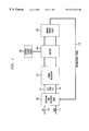
- FIG. 1shows a block diagram of the telephone interface and power supply of a battery operated modem according to the present invention.
- FIG. 2shows a block diagram of a first embodiment of the present invention utilizing a shunt impedance in parallel with the input to a PWM switching power supply.
- FIGS. 3A and 3Bare circuit diagrams of exemplary embodiments of the shunt impedance shown in FIG. 2 .
- FIG. 4is a circuit diagram of an exemplary embodiment of the PWM switching power supply shown in FIG. 2 .
- FIG. 5shows a block diagram of a second embodiment of the present invention utilizing a constant current regulator in series with a PWM switching power supply.
- FIG. 6is an exemplary circuit diagram of the constant current regulator and PWM switching power supply shown in FIG. 5 .
- FIG. 1is a block diagram of a battery powered modem according to the present invention.
- a standard two-wire telephone line 110 , 112 from a central telephone officeis connected to a standard telephone line connector such as an RJ-11 or other common telephone connector (not shown) on the portable computer device.
- the signal from the telephone line 110 , 112includes both an ac signal component and a dc power component and is input to the tip and ring inputs of a telephone line interface 100 of the modem.
- the telephone line interface 100 in the exemplary embodimentis a data access arrangement (DAA) available from LUCENT TECHNOLOGIES.
- the DAA 100includes transformers which provide isolation and balance while minimizing signal distortion within communications networks.
- the DAA 100provides a barrier preventing electrical contact between the modem and the central telephone equipment.
- the transformers in the DAA 100function as an isolation barrier that withstands high voltages between telephone lines, the rest of the modem circuitry, and the user.
- the telephone line interface 100may alternatively be any SLIC chip or telephone interface accepting a common two or four-wire telephone input for a central telephone office.
- the telephone line interface 100extracts both an information signal 118 and a direct current (dc) voltage from the telephone line 110 , 112 .
- the dc voltage component on telephone line 110 , 112is nominally 48 volts dc from the central telephone office, and is extracted from the telephone line 110 , 112 by the telephone line interface 100 and output on power lines 114 , 116 .
- the dc voltagecan be made available for use by a modem on a telephone line essentially only when the modem is in the off hook state
- the present inventionis equally applicable to drawing power from the telephone line in either the off hook or on hook state.
- the exemplary embodiments of the present inventioncomply with present U.S. regulations in drawing power from the telephone line only when the modem is in the off hook state
- the inventioncan also be implemented to draw power from the telephone line in both the off hook and on hook states of the modem.
- a power regulator 102such as a switching regulator or linear regulator converts the dc voltage output from the telephone line interface 100 into a lower voltage, higher current dc voltage.
- the lower voltage, higher current dc voltagecan be added to the power output from a battery 104 to power the portable computer device.
- the output voltage of power regulator 102may be 5 volts, 3.3 volts, 2.5 volts, or any other common power voltage useful for powering circuitry and/or line drivers of a modem.
- the lower voltage, higher current dc voltagecan either be added to the output power of battery 104 , or it can be used to trickle-charge the battery 104 , or both.
- the lower voltage, higher currentcan be used to power only a specific component of the modem circuit 108 , e.g., telephone line interface 100 .
- the battery 104is charged by the power drawn from the telephone line only when the modem is off hook. When the modem is on hook, the battery 104 is charged entirely by an external charge source 106 .
- the output of the battery 104 , the output of the power regulator 102 , and/or the excess power available from the external charge source 106 when plugged into the portable computer devicecombine and assist each other to provide the dc power to the modem circuit 108 and telephone line interface 100 necessary for operation.
- the information signal 118 from the telephone line interface 100is input to the modem circuit 108 , which in the exemplary embodiment comprises a digital signal processor (DSP).
- the information signal 118may include typical telephone quality voice, modulated data, or other standard analog or digital signals conventionally transmitted over a telephone line.
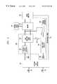
- FIG. 2is a detailed block diagram of an exemplary embodiment of the present invention.
- the telephone line interface 100 , telephone line 110 , 112 , power lines 114 , 116 , external charge source 106 , battery 104 , modem circuitry 108 , and information signal 118are as discussed above with respect to FIG. 1 .
- the power regulator 102comprises a pulse-width modulated (PWM) switching power supply with a shunt impedance which is switched in and out of the circuit.
- PWMpulse-width modulated
- Regulation of the output of the PWM switching power supply 202is accomplished by a feedback loop comprising an error amplifier or comparator 210 which compares the voltage output from the PWM switching power supply 202 to a voltage reference 206 .
- the voltage reference 206outputs a voltage at the desired regulated level, e.g., 5 volts, 3.3. volts, or 2.5 volts.
- a pulse-width modulator 204supplies a PWM switching power supply 202 with a PWM clock signal ‘A’ in which the duty cycle is varied in response to the changing output dc level as determined by error amplifier or comparator 210 .
- PWM clock signal ‘A’is a square wave of variable duty cycle. If the output of the comparator 210 indicates that the voltage output from the PWM switching power supply 202 is low, the positive pulse of PWM clock signal ‘A’ is widened. Conversely, if the output voltage is high, the positive pulse of PWM clock signal ‘A’ is narrowed.
- Inverter 212provides an inverted PWM clock signal ‘/A’ for controlling the switchable shunt impedance 200 .
- Oscillator 208provides an oscillation frequency for pulse-width modulator 204 .
- the frequency of oscillator 208is chosen to correspond to the chosen values of components in the PWM switching power supply 202 , e.g., the value of the capacitor and inductor.
- the frequency of oscillator 208is chosen to be greater than audible frequencies, i.e., approximately 20 KHz and greater.
- the switchable shunt impedance 200is placed in parallel with dc voltage power lines 114 , 116 output from the telephone line interface 100 , and controllably switched in and out of the circuit by the inverted PWM dock signal ‘/A’.
- FIGS. 3A and 3Bare circuit diagrams of exemplary embodiments of the switchable shunt impedance 200 .
- FIG. 3Ashows a resistance or impedance 302 which is switched in and out of the circuit by an NMOS field effect transistor (FET) 300 in correspondence with the positive pulses of the inverted PWM clock signal ‘/A’.
- the resistance or impedance 302 in the exemplary embodimentis a resistor having a resistance approximately equal to the series resistance of the PWM switching power supply 202 and its load.
- a PMOS FET 304 together with resistance or impedance 306can form the switchable shunt impedance 200 as shown in an alternative embodiment shown in FIG. 3 B.
- the switchable shunt impedance 200is switched into the circuit on negative pulses of PWM clock signal ‘A’ to shunt the PWM switching power supply 202 during the time when the PWM switching power supply 202 is not charging its output charge capacitor.
- any suitable semiconductor switchcan be used, e.g., to switch the shunt resistance or impedance 302 , 306 into and out of the circuit.
- the particular semiconductor switch or FET used in the switchable shunt impedance 200need not be the same component used in the PWM switching power supply 202 or other elements of the portable modem device.
- the switchable shunt impedance 200provides a path for a shunt resistance which minimizes load fluctuation presented to the telephone line 110 , 112 arising from the switching of the series-pass FET in the PWM switching power supply. Therefore, noise generated into the telephone line from current chopping by the PWM switching power supply 202 is minimized.
- the PWM switching power supply 202 and switchable shunt impedance 200provide the required load to the telephone line 110 , 112 when the modem is in the off hook state, and maintains a high impedance condition when the modem is in the on hook state, in accordance with present FCC Part 68 regulations in the United States.
- FIG. 4is a circuit diagram of an example PWM switching power supply 202 .
- the switching power supplyhas often been thought of as an on-off device that controls the average direct current passing through it with duty-cycle or pulse-width modulation.
- the PWM switching power supply 202 shown in FIG. 4is a step-down circuit wherein the output voltage is always less than the input voltage.
- the PWM switching power supply 202comprises semiconductor switch 400 , inductor 404 , charge capacitor 406 , and shunt voltage regulator 402 . Reversing the inductor 404 with the diode 402 and inverting the polarity of the capacitor 406 would provide a polarity reversing circuit wherein the output voltage can be greater or less than the input voltage.
- the semiconductor switch 400is an NMOS FET driven by PWM clock signal ‘A’ in the exemplary embodiment.
- the shunt voltage regulator 402 used in the present exemplary embodimentis a free-wheeling diode.
- pulse-width modulator 204outputs a square wave PWM clock signal ‘A’, which switches semiconductor switch 400 closed (or on) and open (or off).
- PWM clock signal ‘A’switches semiconductor switch 400 open (i.e., FET 400 off)
- inductor 404maintains a charge on charge capacitor 406 .
- the inductor 404 , charge capacitor 406 and shunt voltage regulator 402are conventional devices selected according to design parameters shown in Table I.
- Voutis in volts
- Cis in microfarads
- Lis in henries
- Ipkis the peak inductor current in amperes. Table I relates only to the exemplary embodiment of FIG. 4 .
- FIG. 5shows a second exemplary embodiment of the present invention.
- the telephone line interface 100 , telephone lines 110 , 112 , external charge source 106 , battery 104 , modem circuitry 108 , pulse-width modulator 204 , error amplifier 210 , voltage reference 206 , oscillator 208 and information signal 118are as described above.
- the second exemplary embodimentutilizes a constant current regulator 502 together with a PWM switching power supply 500 rather than a switchable shunt impedance 200 as in the first embodiment shown in FIG. 2 .
- the constant current regulator 502 and PWM switching power supply 500are shown in more detail in FIG. 6 .
- a constant current regulator 502is placed in series with a PWM switching power supply 500 to regulate the current drawn by the PWM switching power supply 500 .
- Constant current regulator 502e.g., a diode, lowers its impedance to maintain a constant current flow, and thus presents a nearly constant load to the telephone line dc source, thus generating very little noise back into the telephone line 110 , 112 .
- the value of the current regulationis chosen to allow sufficient charge of charging capacitor 608 when the semiconductor switch 602 is off, and to provide suitable loading to the telephone line 110 , 112 in conformance with telephone standards.
- a shunt semiconductor switch 602is placed in parallel with the input to the PWM switching power supply 500 after the current regulator 502 .
- the semiconductor switch 602may be an NMOS FET as in the present exemplary embodiment.
- the semiconductor switch 602is controlled by an inversion of the PWM clock signal ‘A’, i.e., by inverted PWM clock signal ‘/A’ output from pulse-width modulator 204 .
- the remainder of the PWM switching power supply 500comprises inductor 604 , voltage regulator 606 , and charge capacitor 608 .
- the voltage regulator 606 in the exemplary embodimentis a Zener diode.
Landscapes
- Engineering & Computer Science (AREA)
- Computer Networks & Wireless Communication (AREA)
- Signal Processing (AREA)
- Telephonic Communication Services (AREA)
Abstract
Description


Claims (26)
Priority Applications (1)
| Application Number | Priority Date | Filing Date | Title |
|---|---|---|---|
| US08/907,456US6212226B1 (en) | 1997-08-08 | 1997-08-08 | Supplemental power for battery operated modems |
Applications Claiming Priority (1)
| Application Number | Priority Date | Filing Date | Title |
|---|---|---|---|
| US08/907,456US6212226B1 (en) | 1997-08-08 | 1997-08-08 | Supplemental power for battery operated modems |
Publications (1)
| Publication Number | Publication Date |
|---|---|
| US6212226B1true US6212226B1 (en) | 2001-04-03 |
Family
ID=25424123
Family Applications (1)
| Application Number | Title | Priority Date | Filing Date |
|---|---|---|---|
| US08/907,456Expired - LifetimeUS6212226B1 (en) | 1997-08-08 | 1997-08-08 | Supplemental power for battery operated modems |
Country Status (1)
| Country | Link |
|---|---|
| US (1) | US6212226B1 (en) |
Cited By (16)
| Publication number | Priority date | Publication date | Assignee | Title |
|---|---|---|---|---|
| US6373886B1 (en)* | 2000-01-06 | 2002-04-16 | Pc Tel, Inc. | Power supply circuits for data access arrangement enabling modem operation over a private line |
| US6377667B1 (en)* | 1999-03-15 | 2002-04-23 | 3Com Corporation | Telephone line-assist powered apparatus with programmable hold current |
| US20020076038A1 (en)* | 2000-11-09 | 2002-06-20 | Barrese Michael A. | Telephone line power supply |
| US20030035534A1 (en)* | 1998-04-07 | 2003-02-20 | Keith Eugene Hollenbach | Low noise line powered daa with differential feedback |
| FR2837340A1 (en)* | 2002-03-14 | 2003-09-19 | Jacques Saubade | Switched telephone network connection unit for PDA has modem powered from network through transformer isolated chopper inverter power supply |
| US20030215020A1 (en)* | 2002-05-14 | 2003-11-20 | Ping Dong | Data access arrangement using a high frequency transformer for electrical isolation |
| US6668060B1 (en)* | 1999-10-26 | 2003-12-23 | Adtran, Inc. | Tracking switchmode power converter for telephony interface circuit |
| US6778665B1 (en)* | 1999-10-08 | 2004-08-17 | Agere Systems Inc. | Distribution of current draw in a line powered DAA |
| US6845156B1 (en)* | 2000-02-29 | 2005-01-18 | Agere Systems, Inc. | System for reducing distortion in a line powered modulator |
| US20070258580A1 (en)* | 2004-04-13 | 2007-11-08 | Luciano Gabrielli | Device And A Method For Feeding Electric Devices From A Telephone Line |
| US20090010407A1 (en)* | 2004-10-15 | 2009-01-08 | Grant David S | Communications systems and methods using wireline adapters |
| US20090132679A1 (en)* | 2004-01-13 | 2009-05-21 | Serconet, Ltd. | Information device |
| US20090243572A1 (en)* | 2008-04-01 | 2009-10-01 | Mills Michael J | Power Supply with Digital Control Loop |
| DE102008027110A1 (en)* | 2008-06-06 | 2009-12-10 | Siemens Aktiengesellschaft | Mobile electronic equipment e.g. tablet personal computer, has power supply unit, electronic system, energy storage and communication interface, where electrical power measurable at interface is fed into energy storage |
| US20120002335A1 (en)* | 2010-07-01 | 2012-01-05 | Hon Hai Precision Industry Co., Ltd. | Protection circuit and electronic device using the same |
| US9780601B2 (en) | 2013-06-04 | 2017-10-03 | Seagate Technology Llc | Battery assisted power |
Citations (9)
| Publication number | Priority date | Publication date | Assignee | Title |
|---|---|---|---|---|
| US4373117A (en) | 1980-11-03 | 1983-02-08 | Universal Data Systems, Inc. | DC to DC converter for line powered modem |
| US4415774A (en) | 1981-11-25 | 1983-11-15 | Universal Data Systems, Inc. | Line powered modem automatic answer device powered from equipment |
| US4417099A (en) | 1980-11-03 | 1983-11-22 | Universal Data Systems, Inc. | Electro-optical isolator circuit for line powered modem |
| US4578533A (en) | 1980-11-03 | 1986-03-25 | Universal Data Systems, Inc. | Switchable line powered modem |
| US4691344A (en) | 1986-01-21 | 1987-09-01 | Aquatrol Corporation | Low-powered remote sensor and telephone line transmitter |
| US4803719A (en) | 1987-06-04 | 1989-02-07 | Ulrich Thomas J | Method for powering telephone apparatus and telephone apparatus powered directly from the telephone line without external power |
| US5086454A (en) | 1989-11-17 | 1992-02-04 | Vocal Technologies, Ltd. | Direct connect modem deriving power from telephone line |
| US5461671A (en)* | 1992-06-05 | 1995-10-24 | Murata Mfg. Co., Ltd. | Telephone line power utility circuit |
| US5613229A (en)* | 1995-05-17 | 1997-03-18 | Motorola, Inc. | Voltage and current mode power regulator |
- 1997
- 1997-08-08USUS08/907,456patent/US6212226B1/ennot_activeExpired - Lifetime
Patent Citations (9)
| Publication number | Priority date | Publication date | Assignee | Title |
|---|---|---|---|---|
| US4373117A (en) | 1980-11-03 | 1983-02-08 | Universal Data Systems, Inc. | DC to DC converter for line powered modem |
| US4417099A (en) | 1980-11-03 | 1983-11-22 | Universal Data Systems, Inc. | Electro-optical isolator circuit for line powered modem |
| US4578533A (en) | 1980-11-03 | 1986-03-25 | Universal Data Systems, Inc. | Switchable line powered modem |
| US4415774A (en) | 1981-11-25 | 1983-11-15 | Universal Data Systems, Inc. | Line powered modem automatic answer device powered from equipment |
| US4691344A (en) | 1986-01-21 | 1987-09-01 | Aquatrol Corporation | Low-powered remote sensor and telephone line transmitter |
| US4803719A (en) | 1987-06-04 | 1989-02-07 | Ulrich Thomas J | Method for powering telephone apparatus and telephone apparatus powered directly from the telephone line without external power |
| US5086454A (en) | 1989-11-17 | 1992-02-04 | Vocal Technologies, Ltd. | Direct connect modem deriving power from telephone line |
| US5461671A (en)* | 1992-06-05 | 1995-10-24 | Murata Mfg. Co., Ltd. | Telephone line power utility circuit |
| US5613229A (en)* | 1995-05-17 | 1997-03-18 | Motorola, Inc. | Voltage and current mode power regulator |
Cited By (32)
| Publication number | Priority date | Publication date | Assignee | Title |
|---|---|---|---|---|
| US20030035534A1 (en)* | 1998-04-07 | 2003-02-20 | Keith Eugene Hollenbach | Low noise line powered daa with differential feedback |
| US6731728B2 (en)* | 1998-04-07 | 2004-05-04 | Agere Systems Inc. | Low noise line powered DAA with differential feedback |
| US6377667B1 (en)* | 1999-03-15 | 2002-04-23 | 3Com Corporation | Telephone line-assist powered apparatus with programmable hold current |
| US6778665B1 (en)* | 1999-10-08 | 2004-08-17 | Agere Systems Inc. | Distribution of current draw in a line powered DAA |
| US7076055B2 (en) | 1999-10-26 | 2006-07-11 | Adtran, Inc. | Tracking switchmode power converter for telephony interface circuit |
| US6668060B1 (en)* | 1999-10-26 | 2003-12-23 | Adtran, Inc. | Tracking switchmode power converter for telephony interface circuit |
| US20040076289A1 (en)* | 1999-10-26 | 2004-04-22 | Adtran, Inc. | Tracking switchmode power converter for telephony interface circuit |
| US6373886B1 (en)* | 2000-01-06 | 2002-04-16 | Pc Tel, Inc. | Power supply circuits for data access arrangement enabling modem operation over a private line |
| US6845156B1 (en)* | 2000-02-29 | 2005-01-18 | Agere Systems, Inc. | System for reducing distortion in a line powered modulator |
| US7499539B2 (en)* | 2000-11-09 | 2009-03-03 | Agere Systems, Inc. | Telephone line power supply |
| US20020076038A1 (en)* | 2000-11-09 | 2002-06-20 | Barrese Michael A. | Telephone line power supply |
| FR2837340A1 (en)* | 2002-03-14 | 2003-09-19 | Jacques Saubade | Switched telephone network connection unit for PDA has modem powered from network through transformer isolated chopper inverter power supply |
| US20030215020A1 (en)* | 2002-05-14 | 2003-11-20 | Ping Dong | Data access arrangement using a high frequency transformer for electrical isolation |
| US7277491B2 (en) | 2002-05-14 | 2007-10-02 | Ess Technology, Inc. | Data access arrangement using a high frequency transformer for electrical isolation |
| US20040202204A1 (en)* | 2002-05-14 | 2004-10-14 | Ess Technology, Inc. | Multiplexer |
| US10986165B2 (en) | 2004-01-13 | 2021-04-20 | May Patents Ltd. | Information device |
| US11095708B2 (en) | 2004-01-13 | 2021-08-17 | May Patents Ltd. | Information device |
| US20090132679A1 (en)* | 2004-01-13 | 2009-05-21 | Serconet, Ltd. | Information device |
| US11032353B2 (en) | 2004-01-13 | 2021-06-08 | May Patents Ltd. | Information device |
| US10986164B2 (en) | 2004-01-13 | 2021-04-20 | May Patents Ltd. | Information device |
| US20070258580A1 (en)* | 2004-04-13 | 2007-11-08 | Luciano Gabrielli | Device And A Method For Feeding Electric Devices From A Telephone Line |
| US8050390B2 (en)* | 2004-04-13 | 2011-11-01 | Telecom Italia S.P.A. | Device and a method for feeding electric devices from a telephone line |
| EP1864385A4 (en)* | 2004-10-15 | 2010-09-22 | Universcel Corp | Communications systems and methods using wireline adapters |
| US8229103B2 (en) | 2004-10-15 | 2012-07-24 | Universcel Corporation | Communications systems and methods using wireline adapters |
| US8971524B2 (en) | 2004-10-15 | 2015-03-03 | Universcel Corporation | Communications systems and methods using wireline adapters |
| US9888130B2 (en) | 2004-10-15 | 2018-02-06 | Universcel Corporation | Communications systems and methods using wireline adapters |
| US20090010407A1 (en)* | 2004-10-15 | 2009-01-08 | Grant David S | Communications systems and methods using wireline adapters |
| US20090243572A1 (en)* | 2008-04-01 | 2009-10-01 | Mills Michael J | Power Supply with Digital Control Loop |
| DE102008027110A1 (en)* | 2008-06-06 | 2009-12-10 | Siemens Aktiengesellschaft | Mobile electronic equipment e.g. tablet personal computer, has power supply unit, electronic system, energy storage and communication interface, where electrical power measurable at interface is fed into energy storage |
| US8335066B2 (en)* | 2010-07-01 | 2012-12-18 | Hong Fu Jin Precision Industry (Shenzhen) Co., Ltd. | Protection circuit and electronic device using the same |
| US20120002335A1 (en)* | 2010-07-01 | 2012-01-05 | Hon Hai Precision Industry Co., Ltd. | Protection circuit and electronic device using the same |
| US9780601B2 (en) | 2013-06-04 | 2017-10-03 | Seagate Technology Llc | Battery assisted power |
Similar Documents
| Publication | Publication Date | Title |
|---|---|---|
| US6212226B1 (en) | Supplemental power for battery operated modems | |
| US6215288B1 (en) | Ultra-low power switching regulator method and apparatus | |
| US5717318A (en) | Step-down type DC-DC regulator | |
| CA2001472C (en) | Data circuit-terminating equipment with power source device attached thereto | |
| US5309082A (en) | Hybrid linear-switching power supply | |
| EP0165087A1 (en) | Switching mode power supply | |
| US4779185A (en) | Constant voltage supply system including a constant current source driven switching regulator | |
| CA2320161A1 (en) | Pwm controller for use with open loop dc to ac converter | |
| EP0190110B1 (en) | Voltage convertor for telephone terminal equipment | |
| US6034562A (en) | Mixed signal processing system and method for powering same | |
| US5530636A (en) | Automatic feedback system for a dual output power supply | |
| US5892353A (en) | Power supply apparatus | |
| US6188276B1 (en) | Power amplifier | |
| US6731728B2 (en) | Low noise line powered DAA with differential feedback | |
| EP0225069B1 (en) | Telephone power supply | |
| US6049724A (en) | Ultra-clean voltage power supply generator | |
| US6421430B1 (en) | Line powered DAA with single ended feedback | |
| US4263644A (en) | Current limiter for switched DC-to-DC converter | |
| US5999426A (en) | Circuitry for voltage pole reversal | |
| JP2880940B2 (en) | Mobile phone | |
| EP1213907B1 (en) | switched mode current feed methods for telephony subcriber loops | |
| JPH11332219A (en) | Voltage upconverter for portable tdma radio | |
| US4263645A (en) | Self-starting carrier subscriber power supply | |
| US5963095A (en) | Amplifier circuit, a transmitter and a wireless telephone | |
| Peterson | A frequency-stabilized free-running DC-DC converter circuit employing pulse-width control regulation |
Legal Events
| Date | Code | Title | Description |
|---|---|---|---|
| FEPP | Fee payment procedure | Free format text:PAYOR NUMBER ASSIGNED (ORIGINAL EVENT CODE: ASPN); ENTITY STATUS OF PATENT OWNER: LARGE ENTITY | |
| AS | Assignment | Owner name:LUCENT TECHNOLOGIES, INC., NEW JERSEY Free format text:ASSIGNMENT OF ASSIGNORS INTEREST;ASSIGNOR:NEWTON, KENNETH ALAN;REEL/FRAME:008972/0752 Effective date:19970807 | |
| STCF | Information on status: patent grant | Free format text:PATENTED CASE | |
| FEPP | Fee payment procedure | Free format text:PAYER NUMBER DE-ASSIGNED (ORIGINAL EVENT CODE: RMPN); ENTITY STATUS OF PATENT OWNER: LARGE ENTITY Free format text:PAYOR NUMBER ASSIGNED (ORIGINAL EVENT CODE: ASPN); ENTITY STATUS OF PATENT OWNER: LARGE ENTITY | |
| FPAY | Fee payment | Year of fee payment:4 | |
| FPAY | Fee payment | Year of fee payment:8 | |
| FPAY | Fee payment | Year of fee payment:12 | |
| AS | Assignment | Owner name:DEUTSCHE BANK AG NEW YORK BRANCH, AS COLLATERAL AG Free format text:PATENT SECURITY AGREEMENT;ASSIGNORS:LSI CORPORATION;AGERE SYSTEMS LLC;REEL/FRAME:032856/0031 Effective date:20140506 | |
| AS | Assignment | Owner name:AVAGO TECHNOLOGIES GENERAL IP (SINGAPORE) PTE. LTD Free format text:ASSIGNMENT OF ASSIGNORS INTEREST;ASSIGNOR:AGERE SYSTEMS LLC;REEL/FRAME:035365/0634 Effective date:20140804 | |
| AS | Assignment | Owner name:LSI CORPORATION, CALIFORNIA Free format text:TERMINATION AND RELEASE OF SECURITY INTEREST IN PATENT RIGHTS (RELEASES RF 032856-0031);ASSIGNOR:DEUTSCHE BANK AG NEW YORK BRANCH, AS COLLATERAL AGENT;REEL/FRAME:037684/0039 Effective date:20160201 Owner name:AGERE SYSTEMS LLC, PENNSYLVANIA Free format text:TERMINATION AND RELEASE OF SECURITY INTEREST IN PATENT RIGHTS (RELEASES RF 032856-0031);ASSIGNOR:DEUTSCHE BANK AG NEW YORK BRANCH, AS COLLATERAL AGENT;REEL/FRAME:037684/0039 Effective date:20160201 | |
| AS | Assignment | Owner name:BANK OF AMERICA, N.A., AS COLLATERAL AGENT, NORTH CAROLINA Free format text:PATENT SECURITY AGREEMENT;ASSIGNOR:AVAGO TECHNOLOGIES GENERAL IP (SINGAPORE) PTE. LTD.;REEL/FRAME:037808/0001 Effective date:20160201 Owner name:BANK OF AMERICA, N.A., AS COLLATERAL AGENT, NORTH Free format text:PATENT SECURITY AGREEMENT;ASSIGNOR:AVAGO TECHNOLOGIES GENERAL IP (SINGAPORE) PTE. LTD.;REEL/FRAME:037808/0001 Effective date:20160201 | |
| AS | Assignment | Owner name:AVAGO TECHNOLOGIES GENERAL IP (SINGAPORE) PTE. LTD., SINGAPORE Free format text:TERMINATION AND RELEASE OF SECURITY INTEREST IN PATENTS;ASSIGNOR:BANK OF AMERICA, N.A., AS COLLATERAL AGENT;REEL/FRAME:041710/0001 Effective date:20170119 Owner name:AVAGO TECHNOLOGIES GENERAL IP (SINGAPORE) PTE. LTD Free format text:TERMINATION AND RELEASE OF SECURITY INTEREST IN PATENTS;ASSIGNOR:BANK OF AMERICA, N.A., AS COLLATERAL AGENT;REEL/FRAME:041710/0001 Effective date:20170119 |