US6212220B1 - Method and apparatus for creating non-interfering signals using non-orthogonal techniques - Google Patents
Method and apparatus for creating non-interfering signals using non-orthogonal techniquesDownload PDFInfo
- Publication number
- US6212220B1 US6212220B1US09/255,956US25595699AUS6212220B1US 6212220 B1US6212220 B1US 6212220B1US 25595699 AUS25595699 AUS 25595699AUS 6212220 B1US6212220 B1US 6212220B1
- Authority
- US
- United States
- Prior art keywords
- signal
- repetitive
- channel sequence
- sequence
- combined signal
- Prior art date
- Legal status (The legal status is an assumption and is not a legal conclusion. Google has not performed a legal analysis and makes no representation as to the accuracy of the status listed.)
- Expired - Lifetime
Links
Images

Classifications
- H—ELECTRICITY
- H04—ELECTRIC COMMUNICATION TECHNIQUE
- H04J—MULTIPLEX COMMUNICATION
- H04J13/00—Code division multiplex systems
- H04J13/0007—Code type
- H04J13/0022—PN, e.g. Kronecker
- H—ELECTRICITY
- H04—ELECTRIC COMMUNICATION TECHNIQUE
- H04J—MULTIPLEX COMMUNICATION
- H04J13/00—Code division multiplex systems
- H04J13/10—Code generation
Definitions
- This inventionrelates generally to wireless communication systems, and more particularly to a mechanism for use within a wireless multiple access system, such as a Code Division Multiple Access (CDMA) system, which achieves signal orthogonalization without the use of orthogonal codes.
- CDMACode Division Multiple Access
- the wireless communications industryhas grown enormous in the past twenty years.
- the use of cellular or wireless phones and other such deviceshas been widely accepted by the public.
- the first generation of such cellular telephone devicesoperated on an analog transmission principle using a pair of frequencies per transmission session (sending and receiving) per user.
- Digital cellular devicesoperate by modulating a digital signal onto a carrier wave. Since the signal is digital, certain techniques can then be used to allow multiple users access to the same frequency spectrum, thereby effectively increasing system capacity.
- CDMACode Division Multiple Access
- a single radio frequencyis used as a carrier for the communications of multiple users.
- two CDMA wireless telephone users who are each making a callmay have communications simultaneously transmitted using one or more of the same radio frequencies.
- Each user's signalis encoded with a pseudorandom noise (PN) code at the transmitter in such a way that it can be properly decoded at a received with minimal interference to another user's signal.
- PNpseudorandom noise
- a fading characteristic called Rayleigh fadingoccurs when a transmission signal is reflected from many different features of the physical transmission environment. As a result, the signal arrives at the destination receiver from many directions and each signal may have a different transmission delay. These effects can result in destructive summation of the signals, otherwise known as multi-path fading.
- Certain CDMA modulation techniquescan be used to mitigate the adverse effects of multipath fading and interference, while exploiting frequency reuse advantages.
- One such prior art modulation technique widely implemented in CDMA systemsuses orthogonal codes. Using this technique, a digital data signal to be transmitted is first modulated with a pseudorandom noise (PN) code. The resulting signal is then modulated with an orthogonal code created from an orthogonal code generator to create a user signal which is orthogonal to other user signals. The orthogonal signal can be transmitted on the same frequency as an orthogonal signal created with an another code that is orthogonally related to the first orthogonal code. That is, both orthogonal codes are mathematically interrelated such that the signals produced from the modulations using each code are non-interfering when transmitted on the same frequency together.
- PNpseudorandom noise
- Benefits of digital CDMA systemsinclude a decreased requirement for transmission power which results in longer battery life, increased clarity, higher radio frequency reuse, and favorable signal-to-noise ratio results. Since the frequency spectrum can be reused multiple times in such systems, an overall increase in system user capacity also results.
- the readeris referred to U.S. Pat. No. 4,901,307.
- the present inventionprovides a mechanism to achieve similar results as described above without the use of an orthogonal code generator or orthogonal codes. Instead, a combination of procedures referred to herein as channel sequencing and bit strobing are used to produce two or more resultant signals that do not interfere with one another when transmitted on the same frequency. That is, the resultant signals appear to be, and actually are, orthogonal to one another. However, the process of creating these resultant signals does not require an orthogonal code generator nor orthogonal codes. As such, device power and processing resources can be conserved on a wireless device such as CDMA phone or laptop computer which results in prolonged battery life.
- the inventionprovides a rolling selection of channels with which a modulated information signal can again be modulated.
- the rolling channelsare modulated with the modulated information signal to produce a resultant signal that is double modulated.
- the resultant signalcan be transmitted without interference most of the time.
- a strobe signalis used to alter the selection of the resultant signal.
- the strobe signalessentially reverts to selecting the original singly modulated information signal, instead of the double modulated signal.
- the inventionuses the channel selection and bit strobe mechanism which only requires a secondary modulation process part of the time. At times when the secondary modulation process is not needed, the original modulated signal can be used as a resultant signal without interference. Neither the first nor the second modulation process within this invention requires the use of orthogonal codes. Hence, the invention results in a decrease in the amount of total modulation that is required to be performed and lowers processing and power consumption costs.
- the inventionprovides a system and method for modulating an information signal in a spread spectrum communication system, such as a CDMA communication system.
- An input information signal to be transmittedcan be a digitized voice or data signal generated by a device such as a CDMA phone or modem coupled to a computer.
- the systemuses a first pseudorandom combiner that receives the input information signal and a pseudorandom code sequence.
- the pseudorandom code sequenceis not an orthogonal code sequence.
- the pseudorandom combinercombines the information signal with the pseudorandom code sequence to produce a first combined signal.
- the first combined signalalone may be used at certain times as the resultant signal, without further modulation.
- a channel sequence combinerreceives the first combined signal which includes the information signal in a modulated form.
- the channel sequence combineralso receives a repetitive maximum length channel sequence.
- the repetitive maximum length channel sequenceis also not an orthogonal code.
- the channel sequence combinercombines the first combined signal with the repetitive maximum length channel sequence to produce a second combined signal.
- a selectoris provided which is coupled to receive the first combined signal, the second combined signal and a repetitive strobe signal.
- the selectorselects one of either the first combined signal or the second combined signal to produce a modulated signal based upon a value of the repetitive strobe signal.
- the repetitive strobe signalis of a length greater than the repetitive maximum length channel sequence.
- the repetitive maximum length channel sequenceis a non-orthogonal repeating bit sequence of length N
- the repetitive strobe signalis non-orthogonal repeating bit sequence of at least length N+1.
- the bits 0 through N of the repetitive strobe signalcause the selector to select the second combined signal as the modulated signal and bit N+1 of the repetitive strobe signal selects the first combined signal as the modulated signal.
- the inventioncan produce resultant orthogonal-like signals without the use of orthogonal code generators and/or orthogonal codes.
- a bit from each of the repetitive maximum length channel sequence and the repetitive strobe signalare processed respectively, such that during processing of the first bit of a start of a next cycle of bits from the repetitive maximum length channel sequence by the channel sequence combiner, the selector is processing the last bit of the repetitive strobe signal.
- the repetitive maximum length channel sequenceis a non-orthogonal repeating bit sequence.
- An example of the channel sequenceis 110 .
- the repetitive strobe signalis a non-orthogonal repeating bit sequence, with an example appearing as 0001.
- the system of the inventionis always sure to select a correct non-interfering resultant signal without the use of orthogonal codes and/or orthogonal code generation and modulation techniques.
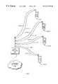
- FIG. 1illustrates a CDMA communications system in which the present invention may be implemented.
- FIG. 2illustrates a block diagram of a non-interfering signal generation process according to this invention.
- FIG. 3illustrates a block diagram of a signal generation system that allows up to four information signals to be simultaneously transmitted on a common frequency without interference.
- FIG. 1illustrates a typical multiple access mobile communications system
- system 100includes mobile subscriber units 101 - 1 , 101 - 2 , 101 - 3 and 101 - 4 (collectively subscribers 101 ) as well as one or more base stations 104 .
- the subscriber units 101provide wireless data (which may include video data, facsimile data, and/or modem data) and/or voice services and can connect devices such as, for example, laptop computers, portable computers, personal digital assistants (PDAs), or the like through base station 104 to a network 105 .
- wireless datawhich may include video data, facsimile data, and/or modem data
- voice servicescan connect devices such as, for example, laptop computers, portable computers, personal digital assistants (PDAs), or the like through base station 104 to a network 105 .
- PDAspersonal digital assistants
- Network 105may be a Public Switch Telephone Network (PSTN), an ISDN network or other circuit-switched network, or may be a connectionless packet based computer network such as the Internet.
- PSTNPublic Switch Telephone Network
- ISDNISDN
- connectionless packet based computer networksuch as the Internet.
- the subscriber units 101may be mobile in nature and may travel from one location to another while communicating in a wireless manner with the base station 104 using the radio frequency transmission techniques of this invention.
- a single base station 104 and four mobile subscribers units 101are shown by way of example only, for ease of description of the invention.
- the inventionis applicable to systems in which there are typically many more subscriber units 101 communicating with one or more, and typically many, base stations 104 .
- the wireless communications systems 100 to which this invention may be appliedare systems that use such techniques as CDMA, TDMA, GSM or other systems where more than one subscriber signal is to be simultaneously transmitted over a common frequency.
- the inventionis applied in a CDMA-like system which uses protocols similar to that specified by the Telecommunications Industry Association (TIA) IS-95 or the newly emerging IS-95B standards.
- TIATelecommunications Industry Association
- the inventionis applicable to any communication systems using multiple access techniques.
- wireless transmission of data over a limited number of radio frequency channel resourcesis provided via forward communication channels 110 - 1 through 110 - 4 , and reverse communication channels 111 - 1 through 111 - 4 .
- the inventionprovides a way to generate the forward and reverse link signals 110 , 111 such that during simultaneous transmission of any two of such signals on the same frequency, the signals 110 , 111 will be non-interfering or orthogonal in nature. The invention accomplishes this without using orthogonal code generators and/or orthogonal codes to generate the signals.
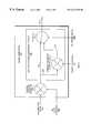
- FIG. 2illustrates a block diagram of a preferred embodiment of the invention which generates an orthogonalized signal without the use of an orthogonal code generator and/or orthogonal codes.
- An initial information signal 200which represents a signal containing user data (or voice) to be transmitted, is input to a pseudorandom combiner 205 .
- PNpseudorandom
- the pseudorandom combiner 205combines the information signal 201 with the pseudorandom code sequence to produce a first combined signal 203 .
- the pseudorandom combiner 205then modulates the information signal 201 with this pseudorandom code sequence 202 .
- the first combined signal 203is then input into a non-orthogonal generation circuit 220 . Within the non-orthogonal generation circuit 220 , the first combined signal is input into each of a channel sequence combiner 210 and a selector 215 .
- the channel sequence combiner 210receives the first combined signal 203 (which includes the modulated information signal 201 ) and also receives a channel sequence 206 .
- the channel sequence 206is a repetitive maximum length channel sequence.
- the channel sequence combiner 210combines the first combine signal 203 with the repetitive maximum length channel sequence 206 , preferably via a modulation technique. As a result of this modulation, the channel sequence combiner 210 outputs a second channel sequence combined signal, or just second combined signal 207 .
- the second combined signal 207represents the modulated information signal 201 (modulated first with the PN sequence 202 ) which is again modulated with the channel sequence 206 .
- the second combined signal 207is also input into the selector 215 , as is the first combined signal 203 .
- the selectoralso receives as input a repetitive strobe signal 208 . Based upon the value of the repetitive strobe signal 208 , the selector 215 selects one of the either the first combined signal 203 (a singly modulated signal) or the second combined signal 207 (the doubly modulated signal) to produce as output a modulated signal 209 .
- the non-orthogonal generation circuit 220then outputs the modulated signal 209 as a resultant signal to be transmitted.
- the period of the repetitive bit strobe signal 208is of a length greater than the repetitive maximum length channel sequence 206 .
- the bit strobe signal 208has a period of at least four bits (i.e., 0001).
- an entire set of channel sequences 206such as 011, 110 and 110, can be cycled through, at which point the strobe signal 208 will be activated to select the first combined signal 203 , instead of the second combined signal 207 .
- the selectorselects for transmission (i.e,, selects as the modulated signal 209 ) the singly modulated first combined signal 203 instead of the second combined signal 207 .
- the modulated signal 209 that is outputwill be orthogonal in nature as compared to another signal created using a corresponding, but offset code channel sequence 206 .
- Table 1illustrates the relationship between the channel sequence values 206 and the repetitive strobe signal values 208 .
- Table 1Channel Sequence 206 in Relation to Bit Strobe Sequence 208
- the top rowis labeled “C” and represents the values of channel sequence 206 .
- the channel sequence 206is a 3-bit rolling code, having values of 111, 110, 101, 011. Note that the value 000 is not used. After the final 011 value, the channel sequence repeats itself beginning again with 111.
- the value of the repetitive bit strobe signal 208is represented in Table 1 by the “B” row.
- the bit strobe 208has a repetitive value of 0001, and endlessly repeats during the operation of information modulation circuit 230 .
- the bit strobeis four bits long and the channel sequence strobe is three bits. Accordingly, at times when the repetitive bit strobe signal 208 has a zero, “0,” or low value, the selector 215 selects the second combined signal 207 . There are three low or “0” values in a row for the repetitive bit strobe signal 208 . As such, the channel sequence combiner 210 is able to modulate three successive channel sequence bits 206 with the first combine signal 203 , and the selector 215 will select as output the second combined signal 207 , before the repetitive bit strobe signal 208 changes to a “1” or high signal. A high or “1” bit strobe signal value 208 then causes the selector 215 to switch states and select the first combine signal 203 , rather than the second combined signal 207 .
- each fourth bit strobe 209will cause the first combined signal 203 to be output which does not include the channel sequence value 206 .
- the resultant modulated output signal 209may be orthogonally combined (i.e., modulated) with other resultant modulated output signals created with other information modulation circuits 230 .
- FIG. 3illustrates this principle.
- four information modulation circuits 230 - 1 , 230 - 2 , 230 - 3 and 230 - 4are provided.
- Each of the four information modulation circuits 230receives a distinct information signal (IS) IS 201 - 1 , IS 201 - 2 , IS 201 - 3 and IS 201 - 4 as input.
- ISinformation signal
- Each information signal 201represents a distinct digital data stream to be transmitted on the same frequency with the other information signals 201 . While the information signal 201 is referred to as a digital data stream, it may be representative of many different types of encoded data, such as voice data, video data, facsimile, data, modem data, or any other type of data.
- each information modulation circuit 230receives a pseudorandom code sequence 202 - 1 , 202 - 2 , 202 - 3 or 202 - 4 that is unique from the other pseudorandom (PN) code sequences 202 .
- each information modulation circuit 230receives an in-phase short pseudorandom (PN) code sequence 202 , although long PN codes may be used as well.
- PNpseudorandom
- Each information modulation circuit 230also receives a channel sequence value 203 - 1 , 203 - 2 , 203 - 3 or 203 - 4 that is offset by one bit from the other channel sequence (CS)values 203 used for the other information modulation circuits 230 .
- CSchannel sequence
- the inventionconverts each information signal 201 into a resultant modulated output signal 209 - 1 through 209 - 4 that will be non-interfering or orthogonal with the others.
- the channel sequence(CS) value 206 - 1 for the information modulation circuit 230 - 1can begin, for example, with a value of “111”.
- the channel sequence(CS) value 206 - 2 for the information modulation circuit 230 - 2can begin with the next channel sequence value “110”.
- the channel sequence(CS) value 206 - 3 for information modulation circuit 230 - 3can begin with the next sequence value “101”, and the final information modulation circuit 230 - 4 begins with a channel sequence(CS) value 206 - 4 of “011.”
- bit strobe signal(BSS) value 208 input into each signal generatoris the same in each case. That is, for the above-identified channel sequences, a repetitive bit strobe signal value of “0001” is used and is a common signal amongst information modulation circuits 230 - 1 through 230 - 4 .
- modulated output signals 209 - 1 through 209 - 4are produced.
- the modulated output signals 209 - 1 through 209 - 4can each be combined together and transmitted on a single frequency without interference, due to how each was created as previously explained.
- oscillators 220 - 1 and 220 - 2are provided to produce oscillation signals 228 - 1 and 228 - 2 which are fed into respective phase splitters 221 - 1 and 221 - 2 .
- Each phase splitter 221 - 1 and 221 - 2divides its respective oscillation signal 228 - 1 or 228 - 2 into first and second phase shifted signals 230 - 1 , 230 - 2 (first phase shifted signals) and 231 - 1 , 231 - 2 (second phase shifted signals), respectively.
- Phase shifted signals 230 - 1 , 230 - 2are preferably one-hundred eighty degrees out-of-phase with one another.
- Modulator 218 - 1then combines the modulated output signal 209 - 1 with the respective phase shifted signal 230 - 1 to produce a summation signal 236 - 1
- the modulator 218 - 2combines the modulated output signal 209 - 2 with its respective phase shifted signal 230 - 2 to produce a summation signal 236 - 2 .
- modulators 218 - 1 and 218 - 2use bipolar phase shift keyed (PSK) modulation and the information signals 201 - 1 and 202 - 2 are the same.
- modulators 218 - 1 and 218 - 2use quadrature phase shift keyed (QPSK) modulation and the information signal 201 - 1 is in an N-State while the information signal 201 - 2 is in an N+1 state.
- PSKphase shift keyed
- QPSKquadrature phase shift keyed
- each information signal 201 - 1 and 201 - 2is different, the information signal 201 - 1 is fed as input to the signal generator 230 - 1 as bit number N, while at the same time, the information signal 201 - 2 is fed as input to the signal generator 230 - 2 as bit N+1.
- information signal 201 - 2is one bit ahead of information signal 201 - 1 .
- the delay in information signal 201 - 1can be accomplished by a simple delay circuit.
- modulator 218 - 3combines the modulated output signal 209 - 3 with its respective phase shifted signal 231 - 1 to produce a summation signal 236 - 3
- modulator 218 - 4combines the modulated output signal 209 - 4 with its respective phase shifted signal 231 - 2 to produce a summation signal 236 - 4 .
- modulators 218 - 3 and 218 - 4can use bipolar phase shift keyed (PSK) modulation and the information signals 201 - 3 and 202 - 4 are the same.
- modulators 218 - 3 and 218 - 4can use quadrature phase shift keyed (QPSK) modulation and the information signal 201 - 3 is in an N-State while the information signal 201 - 4 is in an N+1 state.
- information signal 201 - 4is one bit ahead of information signal 201 - 3 .
- the delay in information signal 201 - 3can be accomplished as noted above by a simple delay circuit.
- summation circuit 239sums each summation signal 236 - 1 through 236 - 4 into a single non-interfering user information signal 240 .
- the inventionallows each of the information signals 201 - 1 through 201 - 4 to be processed as explained above into a single signal 240 without each information signal 201 interfering with the others and without the use of orthogonal codes and orthogonal code generation techniques.
- information signals 201 - 1 through 201 - 4originate from land line connections with the base station and each information signal 201 is associated with (i.e., is destined for) a separate mobile subscriber unit (e.g., 101 - 1 , 101 - 2 , 101 - 3 , 101 - 4 ). That is, in a preferred embodiment, the information signals 201 are transmitted on the forward link (as represented by forward links 110 - 1 through 110 - 4 in FIG. 1) from the base station 104 to the mobile subscriber units 101 - 1 through 101 - 4 .
- the information signals 201 - 1 through 201 - 4can all originate from within a single mobile subscriber unit (i.e., 101 - 1 ) and can be transmitted on the reverse link (i.e., as reverse link signal 111 - 1 ).
- the information signals 201 - 1 through 201 - 4may be, for example, streams of data from a laptop computer or other device, and all four may be required to achieve the necessary bandwidth needed for a particular application in use on the computer.
- a streaming video stream generated by a laptop computer applicationmay be broken into a number of individual digital data streams. Each may be processed as illustrated in FIG. 3 as an individual information signal 201 .
- an ISDN connection serving a video stream, a data stream and a voice streamcan use the invention to combine each stream as one of the information signals 201 into an orthogonally related signal (output signal 240 , to be explained) for transmission on a common frequency.
- the inventionallows very high bandwidth applications to transmit separate but related streams of data, or allows one mobile subscriber device to transmit many unrelated streams of data.
- the receiveri.e. base station 104 in this example
- the receiveris responsible for either re-combining the separate but related information signals 201 or for routing each separate signal to its eventual destination.
Landscapes
- Engineering & Computer Science (AREA)
- Computer Networks & Wireless Communication (AREA)
- Signal Processing (AREA)
- Mobile Radio Communication Systems (AREA)
Abstract
Description
| C | 1 | 1 | 1 | 1 | 1 | 0 | 1 | 0 | 1 | 0 | 1 | 1 | 1 | 1 | 1 | 1 | 0 |
| 0 | 0 | 0 | 1 | 0 | 0 | 0 | 1 | 0 | 0 | 0 | 1 | 0 | 0 | 0 | 1 | 0 | |
Claims (4)
Priority Applications (7)
| Application Number | Priority Date | Filing Date | Title |
|---|---|---|---|
| US09/255,956US6212220B1 (en) | 1999-02-23 | 1999-02-23 | Method and apparatus for creating non-interfering signals using non-orthogonal techniques |
| US09/313,684US6421336B1 (en) | 1999-02-23 | 1999-05-18 | Variable rate orthogonally coded reverse link structure |
| AU34889/00AAU3488900A (en) | 1999-02-23 | 2000-02-11 | Variable rate orthogonally coded reverse link structure |
| EP00913441AEP1155522A1 (en) | 1999-02-23 | 2000-02-11 | Variable rate orthogonally coded reverse link structure |
| PCT/US2000/003591WO2000051276A1 (en) | 1999-02-23 | 2000-02-11 | Variable rate orthogonally coded reverse link structure |
| JP2000601775AJP2002538664A (en) | 1999-02-23 | 2000-02-11 | Variable speed orthogonal coding reverse link structure |
| KR1020017010622AKR100759768B1 (en) | 1999-02-23 | 2000-02-11 | Variable Rate Orthogonal Coded Reverse Link Structure |
Applications Claiming Priority (1)
| Application Number | Priority Date | Filing Date | Title |
|---|---|---|---|
| US09/255,956US6212220B1 (en) | 1999-02-23 | 1999-02-23 | Method and apparatus for creating non-interfering signals using non-orthogonal techniques |
Related Child Applications (1)
| Application Number | Title | Priority Date | Filing Date |
|---|---|---|---|
| US09/313,684Continuation-In-PartUS6421336B1 (en) | 1999-02-23 | 1999-05-18 | Variable rate orthogonally coded reverse link structure |
Publications (1)
| Publication Number | Publication Date |
|---|---|
| US6212220B1true US6212220B1 (en) | 2001-04-03 |
Family
ID=22970543
Family Applications (1)
| Application Number | Title | Priority Date | Filing Date |
|---|---|---|---|
| US09/255,956Expired - LifetimeUS6212220B1 (en) | 1999-02-23 | 1999-02-23 | Method and apparatus for creating non-interfering signals using non-orthogonal techniques |
Country Status (1)
| Country | Link |
|---|---|
| US (1) | US6212220B1 (en) |
Cited By (14)
| Publication number | Priority date | Publication date | Assignee | Title |
|---|---|---|---|---|
| US20020080024A1 (en)* | 2000-02-07 | 2002-06-27 | Tantivy Communications, Inc. | Maintenance link using active/standby request channels |
| US20040223514A1 (en)* | 2000-11-30 | 2004-11-11 | Ipr Licensing, Inc. | Reverse link pilot integrated with block codes |
| US7218623B1 (en) | 2001-05-04 | 2007-05-15 | Ipr Licensing, Inc. | Coded reverse link messages for closed-loop power control of forward link control messages |
| US7551663B1 (en) | 2001-02-01 | 2009-06-23 | Ipr Licensing, Inc. | Use of correlation combination to achieve channel detection |
| US7746830B2 (en) | 1998-06-01 | 2010-06-29 | Interdigital Technology Corporation | System and method for maintaining wireless channels over a reverse link of a CDMA wireless communication system |
| US7773566B2 (en) | 1998-06-01 | 2010-08-10 | Tantivy Communications, Inc. | System and method for maintaining timing of synchronization messages over a reverse link of a CDMA wireless communication system |
| US7936728B2 (en) | 1997-12-17 | 2011-05-03 | Tantivy Communications, Inc. | System and method for maintaining timing of synchronization messages over a reverse link of a CDMA wireless communication system |
| US8134980B2 (en) | 1998-06-01 | 2012-03-13 | Ipr Licensing, Inc. | Transmittal of heartbeat signal at a lower level than heartbeat request |
| US8155096B1 (en) | 2000-12-01 | 2012-04-10 | Ipr Licensing Inc. | Antenna control system and method |
| US8175120B2 (en) | 2000-02-07 | 2012-05-08 | Ipr Licensing, Inc. | Minimal maintenance link to support synchronization |
| US8274954B2 (en) | 2001-02-01 | 2012-09-25 | Ipr Licensing, Inc. | Alternate channel for carrying selected message types |
| US9014118B2 (en) | 2001-06-13 | 2015-04-21 | Intel Corporation | Signaling for wireless communications |
| US9042400B2 (en) | 1997-12-17 | 2015-05-26 | Intel Corporation | Multi-detection of heartbeat to reduce error probability |
| US9525923B2 (en) | 1997-12-17 | 2016-12-20 | Intel Corporation | Multi-detection of heartbeat to reduce error probability |
Citations (5)
| Publication number | Priority date | Publication date | Assignee | Title |
|---|---|---|---|---|
| US4460992A (en) | 1982-11-04 | 1984-07-17 | The United States Of America As Represented By The Secretary Of The Army | Orthogonal CDMA system utilizing direct sequence pseudo noise codes |
| US5103459A (en) | 1990-06-25 | 1992-04-07 | Qualcomm Incorporated | System and method for generating signal waveforms in a cdma cellular telephone system |
| US5559788A (en)* | 1994-12-29 | 1996-09-24 | Unisys Corporation | Multiple channel quadrature communication system and method |
| US5606574A (en)* | 1993-09-13 | 1997-02-25 | Matsushita Electric Industrial Co., Ltd. | Mobile unit identifying system and method of demodulating for the same |
| US5805567A (en)* | 1996-09-13 | 1998-09-08 | Lucent Technologies Inc. | Orthogonal modulation scheme |
- 1999
- 1999-02-23USUS09/255,956patent/US6212220B1/ennot_activeExpired - Lifetime
Patent Citations (6)
| Publication number | Priority date | Publication date | Assignee | Title |
|---|---|---|---|---|
| US4460992A (en) | 1982-11-04 | 1984-07-17 | The United States Of America As Represented By The Secretary Of The Army | Orthogonal CDMA system utilizing direct sequence pseudo noise codes |
| US5103459A (en) | 1990-06-25 | 1992-04-07 | Qualcomm Incorporated | System and method for generating signal waveforms in a cdma cellular telephone system |
| US5103459B1 (en) | 1990-06-25 | 1999-07-06 | Qualcomm Inc | System and method for generating signal waveforms in a cdma cellular telephone system |
| US5606574A (en)* | 1993-09-13 | 1997-02-25 | Matsushita Electric Industrial Co., Ltd. | Mobile unit identifying system and method of demodulating for the same |
| US5559788A (en)* | 1994-12-29 | 1996-09-24 | Unisys Corporation | Multiple channel quadrature communication system and method |
| US5805567A (en)* | 1996-09-13 | 1998-09-08 | Lucent Technologies Inc. | Orthogonal modulation scheme |
Cited By (36)
| Publication number | Priority date | Publication date | Assignee | Title |
|---|---|---|---|---|
| US9525923B2 (en) | 1997-12-17 | 2016-12-20 | Intel Corporation | Multi-detection of heartbeat to reduce error probability |
| US9042400B2 (en) | 1997-12-17 | 2015-05-26 | Intel Corporation | Multi-detection of heartbeat to reduce error probability |
| US7936728B2 (en) | 1997-12-17 | 2011-05-03 | Tantivy Communications, Inc. | System and method for maintaining timing of synchronization messages over a reverse link of a CDMA wireless communication system |
| US7773566B2 (en) | 1998-06-01 | 2010-08-10 | Tantivy Communications, Inc. | System and method for maintaining timing of synchronization messages over a reverse link of a CDMA wireless communication system |
| US9307532B2 (en) | 1998-06-01 | 2016-04-05 | Intel Corporation | Signaling for wireless communications |
| US8792458B2 (en) | 1998-06-01 | 2014-07-29 | Intel Corporation | System and method for maintaining wireless channels over a reverse link of a CDMA wireless communication system |
| US8139546B2 (en) | 1998-06-01 | 2012-03-20 | Ipr Licensing, Inc. | System and method for maintaining wireless channels over a reverse link of a CDMA wireless communication system |
| US8134980B2 (en) | 1998-06-01 | 2012-03-13 | Ipr Licensing, Inc. | Transmittal of heartbeat signal at a lower level than heartbeat request |
| US7746830B2 (en) | 1998-06-01 | 2010-06-29 | Interdigital Technology Corporation | System and method for maintaining wireless channels over a reverse link of a CDMA wireless communication system |
| US8509268B2 (en) | 2000-02-07 | 2013-08-13 | Intel Corporation | Minimal maintenance link to support sychronization |
| US8175120B2 (en) | 2000-02-07 | 2012-05-08 | Ipr Licensing, Inc. | Minimal maintenance link to support synchronization |
| US9301274B2 (en) | 2000-02-07 | 2016-03-29 | Intel Corporation | Minimal maintenance link to support synchronization |
| US7079523B2 (en) | 2000-02-07 | 2006-07-18 | Ipr Licensing, Inc. | Maintenance link using active/standby request channels |
| US9807714B2 (en) | 2000-02-07 | 2017-10-31 | Intel Corporation | Minimal maintenance link to support synchronization |
| US20020080024A1 (en)* | 2000-02-07 | 2002-06-27 | Tantivy Communications, Inc. | Maintenance link using active/standby request channels |
| US9397808B2 (en) | 2000-11-30 | 2016-07-19 | Ipr Licensing, Inc. | Reverse link pilot integrated with block codes |
| US7447187B2 (en) | 2000-11-30 | 2008-11-04 | Ipr Licensing, Inc. | Reverse link pilot integrated with block codes |
| US20040223514A1 (en)* | 2000-11-30 | 2004-11-11 | Ipr Licensing, Inc. | Reverse link pilot integrated with block codes |
| US8830977B2 (en) | 2000-11-30 | 2014-09-09 | Ipr Licensing, Inc. | Reverse link pilot integrated with block codes |
| US20090116469A1 (en)* | 2000-11-30 | 2009-05-07 | Ipr Licensing, Inc. | Reverse link pilot integrated with block codes |
| US8072958B2 (en) | 2000-11-30 | 2011-12-06 | Ipr Licensing, Inc. | Reverse link pilot integrated with block codes |
| US9924468B2 (en) | 2000-12-01 | 2018-03-20 | Intel Corporation | Antenna control system and method |
| US8437330B2 (en) | 2000-12-01 | 2013-05-07 | Intel Corporation | Antenna control system and method |
| US8155096B1 (en) | 2000-12-01 | 2012-04-10 | Ipr Licensing Inc. | Antenna control system and method |
| US9775115B2 (en) | 2000-12-01 | 2017-09-26 | Intel Corporation | Antenna control system and method |
| US9225395B2 (en) | 2000-12-01 | 2015-12-29 | Intel Corporation | Antenna control system and method |
| US9247510B2 (en) | 2001-02-01 | 2016-01-26 | Intel Corporation | Use of correlation combination to achieve channel detection |
| US7551663B1 (en) | 2001-02-01 | 2009-06-23 | Ipr Licensing, Inc. | Use of correlation combination to achieve channel detection |
| US8687606B2 (en) | 2001-02-01 | 2014-04-01 | Intel Corporation | Alternate channel for carrying selected message types |
| US8638877B2 (en) | 2001-02-01 | 2014-01-28 | Intel Corporation | Methods, apparatuses and systems for selective transmission of traffic data using orthogonal sequences |
| US8274954B2 (en) | 2001-02-01 | 2012-09-25 | Ipr Licensing, Inc. | Alternate channel for carrying selected message types |
| US7218623B1 (en) | 2001-05-04 | 2007-05-15 | Ipr Licensing, Inc. | Coded reverse link messages for closed-loop power control of forward link control messages |
| US9019930B2 (en) | 2001-05-04 | 2015-04-28 | Ipr Licensing, Inc. | Coded reverse link messages for closed-loop power control of forward link control messages |
| US20070206542A1 (en)* | 2001-05-04 | 2007-09-06 | Interdigital Technology Corporation | Coded reverse link messages for closed-loop power control of forward link control messages |
| US8737343B2 (en) | 2001-05-04 | 2014-05-27 | Ipr Licensing, Inc. | Coded reverse link messages for closed-loop power control of forward link control messages |
| US9014118B2 (en) | 2001-06-13 | 2015-04-21 | Intel Corporation | Signaling for wireless communications |
Similar Documents
| Publication | Publication Date | Title |
|---|---|---|
| RU2313176C2 (en) | Client block and method for using it in a wireless communication system | |
| US9467200B2 (en) | Method and apparatus for orthogonally overlaying variable chip rate spread spectrum signals | |
| US5515396A (en) | Method and apparatus for selecting a spreading code in a spectrum spread communication system | |
| KR100353641B1 (en) | Base station transmit antenna diversity apparatus and method in cdma communication system | |
| JP3526741B2 (en) | Method for transmitting two parallel channels using code division and apparatus for implementing the method | |
| US6424619B2 (en) | High data rate CDMA wireless communication system | |
| US6678311B2 (en) | High data CDMA wireless communication system using variable sized channel codes | |
| US5926500A (en) | Reduced peak-to-average transmit power high data rate CDMA wireless communication system | |
| US6389138B1 (en) | Method and apparatus for generating a complex scrambling code sequence | |
| EP1110360B1 (en) | Method and apparatus for reducing amplitude variations in communication signals employing inserted pilot symbols | |
| US6212220B1 (en) | Method and apparatus for creating non-interfering signals using non-orthogonal techniques | |
| US5892774A (en) | Phase shift encoded subchannel | |
| KR100343089B1 (en) | A method and apparatus for facilitating multi-rate data transmission by selecting a plurality of spreading codes | |
| EP0854586B1 (en) | Quadrature spread spectrum signal demodulation | |
| US6421336B1 (en) | Variable rate orthogonally coded reverse link structure | |
| US6535478B2 (en) | Reduced peak-to-average amplitude multichannel link | |
| US7433385B1 (en) | Code division multiple access communication |
Legal Events
| Date | Code | Title | Description |
|---|---|---|---|
| AS | Assignment | Owner name:TANTIVY COMMUNICATIONS, INC., FLORIDA Free format text:ASSIGNMENT OF ASSIGNORS INTEREST;ASSIGNORS:PROCTOR, JAMES A. JR.;HOFFMANN, JOHN E.;ROUPHAEL, ANTOINE J.;REEL/FRAME:009799/0407 Effective date:19990205 | |
| AS | Assignment | Owner name:TRANSAMERICA BUSINESS CREDIT CORPORATION, CONNECTI Free format text:SECURITY AGREEMENT;ASSIGNOR:TANTIVY COMMUNICATIONS, INC.;REEL/FRAME:010108/0827 Effective date:19990610 | |
| STCF | Information on status: patent grant | Free format text:PATENTED CASE | |
| AS | Assignment | Owner name:TANTIVY COMMUNICATIONS, INC., FLORIDA Free format text:ASSIGNMENT OF ASSIGNORS INTEREST;ASSIGNOR:PROCTOR, JAMES A., JR.;REEL/FRAME:011874/0766 Effective date:20010108 | |
| AS | Assignment | Owner name:SILICON VALLEY BANK, CALIFORNIA Free format text:SECURITY AGREEMENT;ASSIGNOR:TANTIVY COMMUNICATIONS, INC.;REEL/FRAME:012506/0808 Effective date:20011130 | |
| AS | Assignment | Owner name:IPR HOLDINGS DELAWARE, INC., DELAWARE Free format text:ASSIGNMENT OF ASSIGNORS INTEREST;ASSIGNOR:TANTIVY COMMUNICATIONS, INC.;REEL/FRAME:013067/0204 Effective date:20020812 Owner name:IPR HOLDINGS DELAWARE, INC., DELAWARE Free format text:LICENSE;ASSIGNOR:TANTIVY COMMUNICATIONS, INC.;REEL/FRAME:013067/0204 Effective date:20020812 | |
| AS | Assignment | Owner name:IPR HOLDINGS DELAWARE, INC., PENNSYLVANIA Free format text:SECURITY INTEREST;ASSIGNOR:TANTIVY COMMUNICATIONS, INC.;REEL/FRAME:014289/0207 Effective date:20030722 | |
| AS | Assignment | Owner name:INTERDIGITAL PATENT CORPORATION, DELAWARE Free format text:ASSIGNMENT OF ASSIGNORS INTEREST;ASSIGNOR:INTERDIGITAL ACQUISITION CORPORATION;REEL/FRAME:014351/0777 Effective date:20040218 | |
| AS | Assignment | Owner name:INTERDIGITAL ACQUISITION CORP., DELAWARE Free format text:ASSIGNMENT OF ASSIGNORS INTEREST;ASSIGNOR:TANTIVY COMMUNICATIONS, INC.;REEL/FRAME:015000/0141 Effective date:20030730 Owner name:INTERDIGITAL PATENT CORPORATION, DELAWARE Free format text:MERGER;ASSIGNOR:INTERDIGITAL ACQUISITION CORP.;REEL/FRAME:015000/0577 Effective date:20040218 | |
| AS | Assignment | Owner name:IPR LICENSING, INC., DELAWARE Free format text:ASSIGNMENT OF ASSIGNORS INTEREST;ASSIGNOR:INTERDIGITAL PATENT CORPORATION;REEL/FRAME:014420/0435 Effective date:20040309 | |
| FPAY | Fee payment | Year of fee payment:4 | |
| FPAY | Fee payment | Year of fee payment:8 | |
| AS | Assignment | Owner name:IPR HOLDINGS DELAWARE, INC., DELAWARE Free format text:LICENSE;ASSIGNOR:TANTIVY COMMUNICATIONS, INC.;REEL/FRAME:028349/0387 Effective date:20020822 Owner name:TANTIVY COMMUNICATIONS, INC., FLORIDA Free format text:RELEASE BY SECURED PARTY;ASSIGNOR:SILICON VALLEY BANK;REEL/FRAME:028345/0179 Effective date:20061206 Owner name:TANTIVY COMMUNICATIONS, INC., FLORIDA Free format text:RELEASE BY SECURED PARTY;ASSIGNOR:TRANSAMERICA BUSINESS CREDIT CORPORATION;REEL/FRAME:028343/0888 Effective date:20020301 Owner name:TANTIVY COMMUNICATIONS, INC., FLORIDA Free format text:RELEASE BY SECURED PARTY;ASSIGNOR:SILICON VALLEY BANK;REEL/FRAME:028339/0500 Effective date:20030423 | |
| FPAY | Fee payment | Year of fee payment:12 |