US6211960B1 - Method and apparatus for aligning and connecting semiconductor components to substrates - Google Patents
Method and apparatus for aligning and connecting semiconductor components to substratesDownload PDFInfo
- Publication number
- US6211960B1 US6211960B1US09/300,362US30036299AUS6211960B1US 6211960 B1US6211960 B1US 6211960B1US 30036299 AUS30036299 AUS 30036299AUS 6211960 B1US6211960 B1US 6211960B1
- Authority
- US
- United States
- Prior art keywords
- platform
- component
- substrate
- contacts
- camera
- Prior art date
- Legal status (The legal status is an assumption and is not a legal conclusion. Google has not performed a legal analysis and makes no representation as to the accuracy of the status listed.)
- Expired - Lifetime
Links
- 239000000758substrateSubstances0.000titleclaimsabstractdescription107
- 239000004065semiconductorSubstances0.000titleclaimsabstractdescription59
- 238000000034methodMethods0.000titleabstractdescription28
- 239000000523sampleSubstances0.000claimsabstractdescription35
- 238000012360testing methodMethods0.000claimsabstractdescription35
- 235000012431wafersNutrition0.000claimsabstractdescription29
- 241000238631HexapodaSpecies0.000claimsabstractdescription12
- 238000004891communicationMethods0.000claimsdescription15
- 230000007246mechanismEffects0.000claimsdescription15
- 230000003287optical effectEffects0.000claimsdescription3
- 230000013011matingEffects0.000abstractdescription3
- 230000008569processEffects0.000description11
- 238000004519manufacturing processMethods0.000description9
- 229910000679solderInorganic materials0.000description6
- 238000004806packaging method and processMethods0.000description5
- 239000000853adhesiveSubstances0.000description3
- 230000001070adhesive effectEffects0.000description3
- 239000012790adhesive layerSubstances0.000description3
- 238000009826distributionMethods0.000description3
- 230000000007visual effectEffects0.000description3
- 238000012423maintenanceMethods0.000description2
- 238000010998test methodMethods0.000description2
- 238000004026adhesive bondingMethods0.000description1
- 239000000969carrierSubstances0.000description1
- 239000000919ceramicSubstances0.000description1
- 238000010924continuous productionMethods0.000description1
- 238000013461designMethods0.000description1
- 230000009977dual effectEffects0.000description1
- 230000000694effectsEffects0.000description1
- 239000013536elastomeric materialSubstances0.000description1
- 238000007373indentationMethods0.000description1
- 239000007788liquidSubstances0.000description1
- 238000012986modificationMethods0.000description1
- 230000004048modificationEffects0.000description1
- 230000000149penetrating effectEffects0.000description1
- 230000000737periodic effectEffects0.000description1
- 229920001296polysiloxanePolymers0.000description1
- 238000012545processingMethods0.000description1
- 230000004044responseEffects0.000description1
- 125000006850spacer groupChemical group0.000description1
Images


Classifications
- H—ELECTRICITY
- H01—ELECTRIC ELEMENTS
- H01L—SEMICONDUCTOR DEVICES NOT COVERED BY CLASS H10
- H01L21/00—Processes or apparatus adapted for the manufacture or treatment of semiconductor or solid state devices or of parts thereof
- H01L21/67—Apparatus specially adapted for handling semiconductor or electric solid state devices during manufacture or treatment thereof; Apparatus specially adapted for handling wafers during manufacture or treatment of semiconductor or electric solid state devices or components ; Apparatus not specifically provided for elsewhere
- H01L21/68—Apparatus specially adapted for handling semiconductor or electric solid state devices during manufacture or treatment thereof; Apparatus specially adapted for handling wafers during manufacture or treatment of semiconductor or electric solid state devices or components ; Apparatus not specifically provided for elsewhere for positioning, orientation or alignment
- H01L21/681—Apparatus specially adapted for handling semiconductor or electric solid state devices during manufacture or treatment thereof; Apparatus specially adapted for handling wafers during manufacture or treatment of semiconductor or electric solid state devices or components ; Apparatus not specifically provided for elsewhere for positioning, orientation or alignment using optical controlling means
Definitions
- This inventionrelates to semiconductor manufacture, and more particularly to a method and apparatus for aligning and bonding semiconductor components, such as bare dice and chip scale packages, to a substrate, such as an interconnect, or a printed circuit board.
- Semiconductor componentsare used in the fabrication of electronic items, such as multi chip modules.
- bare semiconductor dicecan be mounted to substrates such as printed circuit boards, and ceramic interposers.
- Flip chip mounting of bumped diceis one method for electrically connecting the dice to the substrates. With flip chip mounting, solder bumps on the device bond pads are reflowed into electrical contact with contacts on the substrate.
- Chip on board (COB) mounting of dice to substratescan also be employed. With chip on board mounting, wire bonds are formed between the device bond pads and contacts on the substrate.
- Chip scale packagesare sometimes used in place of bare dice for fabricating electronic items.
- a chip scale packageincludes a substrate bonded to the face of a bare die.
- the substrateincludes the external contacts for making outside electrical connections to the chip scale package.
- the external contacts for one type of chip scale packageinclude solder balls arranged in a dense array, such as a ball grid array (BGA), or a fine ball grid array (FBGA).
- BGAball grid array
- FBGAfine ball grid array
- chip scale packagescan be mounted to substrates using the same mounting methods employed with bare dice (e.g., flip chip, COB).
- the substrateincludes contacts that must be physically aligned with, and then electrically connected to corresponding contacts on the component.
- the contactsbecome denser, aligning and electrically connecting the components to substrates become more difficult. Accordingly, a key design consideration in the packaging and testing of semiconductor components, is the method for aligning and connecting the components to the mating substrates.
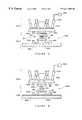
- FIG. 1An example of a test assembly for semiconductor components is shown in FIG. 1 .
- the test assemblyincludes a carrier 2 adapted to temporarily package a semiconductor component 9 for testing.
- the component 9includes contacts 11 in electrical communication with integrated circuits on the component 9 .
- Mounted within the carrier 2is an interconnect 4 .
- the interconnectcan be attached to the carrier 2 using an adhesive layer 6 .
- Included on the interconnect 4are patterns of contacts 8 configured to make separate electrical connections with the contacts 11 on the component 9 .
- Exemplary carriers and interconnectsare more fully described in U.S. Pat. Nos. 5,519,332 and 5,541,525 to Wood et al.
- the interconnect 4is the substrate to which the component 9 must be aligned and connected.
- An assembly devicecan be used for aligning and connecting the component 9 to the interconnect 4 .
- This type of assembly deviceis described in the above cited patents, and also in U.S. Pat. No. 5,634,267 to Wood et al. In general the assembly device aligns the component and the interconnect, and then brings the component and interconnect together to place the contacts on the component in electrical communication with the contacts on the interconnect.
- the tips of the contacts 8 on the interconnect 4are preferably in the same plane, and the surfaces of the contacts 11 on the component 9 are preferably in the same plane. However, this may not always be the case.
- the contacts 8 on the interconnect 4are preferably parallel to either the top or the bottom surfaces of the carrier 2 , because these surfaces can be used to mount the carrier 2 to the assembly device.
- the plane containing the contacts 8is rarely parallel to either the top or the bottom surface of carrier 2 . This makes the alignment and connecting process more difficult because these differences in planarity can cause misalignment between the contacts 8 on the interconnect 4 and the contacts 11 on the component 9 .
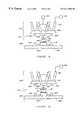
- FIG. 2another interconnect 4 A is shown attached to another carrier 2 A using an adhesive layer 6 A.
- Contacts 8 A on the interconnect 4 Aare designed to be electrically connected to the contacts 11 on the component 9 which is being held by a vacuum quill 7 of the assembly device.
- Plane Ais the plane containing the bottom surface of the carrier 2 A.
- Plane Bis the plane containing the bottom surface of interconnect 4 A.
- Plane Cis the plane containing the top surface of the interconnect 4 A.
- Plane Dis the plane containing the contacts 8 A.
- Plane Eis the plane containing the surface of component 9 and the contacts 11 .
- planes B, C and DDue to the fabrication process that is used to manufacture interconnects, planes B, C and D can be made substantially planar. However, due to variations in the thickness of the adhesive layer 6 A, planes B, C and D are rarely parallel to plane A. Accordingly, even if plane E can be properly oriented with respect to plane A, plane E is not necessarily parallel to or appropriately aligned with plane D or contacts 8 A.
- One aspect of prior art assembly devicesis that most devices are typically able to align the component and interconnect in only four degrees of freedom (X, Y, Z, ⁇ ). Alignment of the component and interconnect in the other two degrees of freedom ( ⁇ , ⁇ ) is usually not performed. Accordingly, when the component and interconnect are moved together in the Z-axis direction, the contacts on the component may not always engage the contacts on the interconnect along the same plane. This misalignment can cause pivoting of the component, or interconnect, and further misalignment. Also, the potential of misalignment can require overdriving the component, or the interconnect, in the Z-axis direction to make reliable electrically connections. This overdrive can damage the contacts on the components and substrate.
- aligner bonder toolscan be used to align and then bond semiconductor dice to a substrate.
- a representative aligner bonder toolis disclosed in U.S. Pat. No. 4,899,921 to Bendat et al. These types of tools typically require two separate platforms whose movement must be coordinated.
- split vision optics with movable optical probescan be required to view aligned portions of the dice and substrate. The different types of mechanisms required for alignment and optics makes aligner bonder tools relatively complicated and difficult to operate with high precision.
- probe testingAnother example of a semiconductor process involving alignment occurs during wafer probe testing.
- a probe cardmust be aligned and placed in electrical contact with the wafer.
- needle probesmake the electrical connections with contacts on the wafer. Routine maintenance of these probe cards includes checking the position of the needle probes in relation to the contacts on the wafer. However, even with periodic maintenance, the tips of the needle probes can be misaligned in the X, Y and Z-directions. Consequently, some of the needle probes may be misaligned with the contacts on the wafer. The same situation can occur due to differences in the X, Y and Z-direction locations of the contacts on the wafer. If the needle probes cannot flex enough to compensate for misalignment, then the resultant electrical connections can be poor.
- alignment problemscan occur in other semiconductor packaging or assembly processes such as wire bonding and adhesive bonding of dice to leadframes.
- Another manufacturing process involving alignmentoccurs during fabrication of flat panel field emission displays (FEDs).
- An individual field emission display pixelincludes emitter sites formed on a baseplate. Electrons emitted by the emitter sites strike phosphors contained on a display screen to form an image. During fabrication of the field emission display it is necessary to align the baseplate with the display screen.
- field emission displaysare typically constructed as a sealed package with a vacuum space between the baseplate and the display screen. This spaces complicates the alignment procedure because most alignment devices, such as aligner bonder tools, are constructed to bring the mating components into physical contact.
- an assembly device for semiconductor componentsto be capable of alignment in six degrees of freedom including three translational degrees of freedom (X, Y, Z) and three rotational degrees of freedom ( ⁇ , ⁇ , ⁇ ).
- the present inventionis directed to an automated assembly device capable of alignment in six degrees of freedom.
- the assembly devicecan align semiconductor components, or substrates, in three translational and three rotational degrees of freedom, while maintaining a high degree of accuracy and speed.
- a method and apparatus for aligning and connecting a semiconductor component and a substrateare provided.
- the apparatusincludes a platform assembly and a chuck assembly.
- the platform assemblyis configured to move one object, either the component or substrate, in six degrees of freedom (X, Y, Z, ⁇ , ⁇ , ⁇ ), as the other object is held stationary by the chuck assembly. This enables alignment and physical contact to be achieved with a high degree of precision.
- the platform assemblycomprises a hexapod, and includes a fixed platform and a moving platform.
- the moving platformis coupled to the fixed platform by six linear actuators.
- the moving platformincludes a holding mechanism for holding the moving object, either the component or the substrate, for movement therewith.
- the linear actuatorsrequire minimal movement and control to effect movement of the moving platform and moving object in six degrees of freedom.
- the alignment of the component with the substrateis accomplished through the use of cameras and height gauges mounted on the moving platform and the chuck assembly.
- the camerasare capable of obtaining images of the facing surfaces of the component and substrate.
- the height gaugesare capable of determining the distances between the gauges and facing surfaces of the component and substrate.
- the camerasconvert the images into electronic signals which are transmitted to a controller, such as a computer or CPU.
- the height gaugestransmit electronic signals of the distance data to the controller as well.
- the controllerutilizes the image information, and the distance information, to determine the relative rotational axis orientation ( ⁇ , ⁇ , ⁇ ), of the facing surface of the component, relative to the rotational axis orientation ( ⁇ , ⁇ , ⁇ ) of the facing surface of the substrate.
- the controllercan also utilize the information to identify the X, Y and Z coordinates of the contacts on the component and substrate. Upon determining the X, Y and Z coordinates of the contacts, and the relative rotational axis orientation of the planes of the contacts, the controller operates the linear actuators of the platform assembly to move the moving object into alignment and physical contact with the stationary object.
- the method of the present inventionincludes the steps of: providing a platform assembly capable of moving a semiconductor component, or a substrate, in three degrees of translational freedom and three degrees of rotational freedom, the platform assembly comprising a hexapod; providing a chuck assembly for holding the component, or the substrate, proximate to the platform assembly; determining the position and orientation of contacts on the component and contacts on the substrate; moving the platform assembly responsive to the determining step until the contacts on the component and substrate are spatially aligned and parallel; and operating the platform assembly responsive to the determining step to move the component into contact with the substrate.
- FIG. 1is a cross-sectional view of a prior art carrier containing a semiconductor component and an interconnect;
- FIG. 2is a cross-sectional view of a prior art test carrier and a semiconductor component being aligned and connected to an interconnect of the carrier using an assembly device;
- FIG. 3is an exploded view of a component and a substrate during an aligning and connecting process performed in accordance with the invention
- FIG. 3Ais an enlarged schematic cross sectional view of a planar contact on a semiconductor component electrically connected to a contact on a substrate;
- FIG. 3Bis an enlarged schematic cross sectional view of a bumped contact on a semiconductor component electrically connected to a contact on a substrate;
- FIG. 3Cis an enlarged schematic cross sectional view of the bumped contact on a semiconductor component electrically connected to a contact on a substrate;
- FIG. 4is a schematic cross-sectional view of an apparatus constructed in accordance with the invention.
- FIG. 5is a schematic cross-sectional view of an alternate embodiment apparatus constructed in accordance with the invention for assembling a test carrier
- FIG. 6is schematic cross-sectional view of an alternate embodiment apparatus constructed in accordance with the invention for assembling a test carrier
- FIG. 7is a schematic cross-sectional view of an alternate embodiment apparatus constructed in accordance with the invention for attaching a die to a leadframe;
- FIG. 8is a schematic cross-sectional view of an alternate embodiment apparatus constructed in accordance with the invention for wire bonding a die to a leadframe;
- FIG. 9is a schematic cross-sectional view of an alternate embodiment apparatus constructed in accordance with the invention for probe testing semiconductor wafers.
- FIG. 10is a schematic cross-sectional view of an alternate embodiment apparatus constructed in accordance with the invention for assembling a field emission display (FED).
- FEDfield emission display
- the component 10includes a facing surface 13 with a plurality of component contacts 14 formed thereon.
- the substrate 12includes a facing surface 15 with a plurality of substrate contacts 16 formed thereon.
- FIGS. 3A-3Billustrate exemplary components 10 and substrates 12 .
- the componentcomprises a semiconductor die 10 A and the component contacts comprise bond pads 14 A on the face (circuit side) of the die 10 A.
- the substratecomprises an interconnect 12 A and the substrate contacts comprise contact members 16 A.
- the contact members 16 Aare adapted to establish temporary electrical connections with the bond pads 14 A for testing.
- Interconnect 12 Ais more fully described in U.S. Pat. No. 5,483,741 to Akram et al., incorporated herein by reference.
- the componentcomprises a chip scale package 10 B, and the component contacts comprise solder bumps 14 B formed on a BGA substrate of the package 10 B.
- the substratecomprises an interconnect 12 B and the substrate contacts comprise contact members 16 B adapted to establish temporary electrical connections with the solder bumps.
- Interconnect 12 Bis more fully described in U.S. patent application Ser. No. 08/823,490, now U.S. Pat. No. 6,016,060, entitled “Method, Apparatus And System For Testing Bumped Semiconductor Components”, incorporated herein by reference.
- the componentagain comprises the chip scale repackage 10 B and the component contacts comprise the solder bumps 14 B.
- the substratecomprises an interconnect 12 C and the substrate contacts comprise indentation contact members 16 C adapted to retain and electrically contact the solder bumps 14 B.
- Interconnect 12 Cis more fully described in U.S. patent application Ser. No. 08/829,193, now U.S. Pat. No. 5,962,921, entitled “Interconnect Having Recessed Contact Members With Penetrating Blades For Testing Semiconductor Dice And Packages With Contact Bumps”, incorporated herein by reference.
- the substrate contacts 16form separate electrical connections with the component contacts 14 for testing.
- the moving objectis moved with a Z-direction component, to achieve physical contact between the substrate contacts 16 and the component contacts 14 .
- the apparatus 20comprises two primary components, a platform assembly 22 and a chuck assembly 24 .
- the chuck assembly 24holds one object, for example, the substrate 12 , in a fixed position and orientation.
- the platform assembly 22holds a second object, for example, the component 10 .
- the platform assembly 22is able to move the component 10 in six degrees of freedom, namely three translational degrees of freedom (X, Y, Z) and three rotational degrees of freedom ( ⁇ , ⁇ , ⁇ ).
- the degrees of freedomcan be according to conventional definitions wherein the X-axis and Y-axis are orthogonal and co-planar, and the Z-axis is contained in a plane orthogonal to the plane of the X-axis and Y-axis.
- ⁇can be angular rotation about the Z-axis
- ⁇can be angular rotation about the Y-axis
- ⁇can be angular rotation about the X-axis.
- the three rotational degrees of freedomare also sometimes referred to as pitch, yaw and roll.
- the platform assembly 22comprises a hexapod, or Stewart platform.
- the platform assembly 22includes a fixed platform 30 and a moving platform 32 .
- the moving platform 32is connected to the fixed platform 30 by a plurality of linear actuators 34 .
- the linear actuators 34are preferably connected to the fixed platform 30 and to the moving platform 32 by universal ball joints 36 at each end thereof. While universal ball joints 36 are preferred, other connection mechanisms allowing sufficient freedom of movement could be utilized without departing from the spirit and scope of the present invention.
- the linear actuators 34are preferably controlled by a controller 46 such as a computer controller, or a central processing unit (CPU). In general the controller 46 must possess sufficient computing power to precisely control the six linear actuators 34 .
- the platform assembly 22also includes a holding mechanism 38 attached to the moving platform 32 for holding the component 10 .
- the holding mechanism 38is configured to hold the component 10 in a fixed relationship relative to the moving platform 32 , such that the component 32 moves with the moving platform 32 .
- One type of holding mechanism 38 suitable for this applicationis a vacuum quill. Vacuum quills are known in the art and utilized in handling semiconductor components in a variety of systems (e.g., semiconductor pick and place mechanisms).
- the chuck assembly 24is stationary and holds the substrate 12 in a fixed position and orientation.
- the chuck assembly 24includes a chuck 40 that fixedly retains the substrate 26 during the aligning and connecting process, and then subsequently allows release. While in the apparatus 20 of FIG. 4, the component 10 is mounted for movement by the platform assembly 22 , and the substrate 12 is held stationary by the chuck assembly 24 this could be reversed. Specifically, the component 10 could be held by the chuck assembly 24 and the substrate 12 moved by the platform assembly 22 .
- the position and orientation of substrate 12is accomplished through the use of a height gauge 42 and a camera 44 mounted on the moving platform 32 .
- a laser height gaugeis preferred, other distance measuring devices such as an interferometer can also be employed.
- the height gauge 42 and camera 44are configured for attachment to the moving platform 32 , and are sized to allow clearance from the items mounted on chuck assembly 24 during the aligning and connecting process.
- the height gauge 42 and camera 44could also be mounted independently of the moving platform 32 . In this case the height gauge 42 and camera can be mounted for movement on an X, Y and Z translational stage.
- an X, Y, Z translational stagecan be used to accomplish large movement, while the moving platform 32 is used to accomplish alignment and fine movement.
- dual moving platforms 32can be employed or one moving platform can be mounted on another moving platform.
- the height gauge 42 and camera 44are in signal communication with the controller 46 which operates the linear actuators 34 .
- the height gauge 42 and camera 44generate electronic signals which are transmitted to the controller 46 .
- the controller 46is configured to receive and analyze the signals and to operate the linear actuators 36 in response to the signals.
- the moving platform 32can be moved such that the height gauge 42 is proximate to the substrate 12 , and is able to determine the distance between the height gauge 42 and the substrate 12 .
- This distance informationcan be converted into a signal, which can be optically or electrically transmitted to the controller 46 .
- the distance informationgives a Z-axis coordinate for the substrate 12 .
- the moving platform 32can be moved such that the camera 44 is proximate to the substrate 12 and can generate an image of the facing surface 15 of the substrate 12 .
- the visual imagecan be used to identify three reference points X 1 , X 2 , X 3 (FIG. 3) on the facing surface 15 .
- the references points X 1 , X 2 , X 3can be known features of the substrate 12 , such as the substrate contacts 16 , or can be dedicated alignment fiducials formed on the substrate 12 . This image is then converted into a signal which can be optically or electrically transmitted to the controller 46 .
- the position and orientation of the plane containing the reference pointscan be determined. This calculation can be performed by the controller 46 or can be performed by another computer (not shown) in signal communication with the controller 46 .
- the position and orientation of the component 10can be determined in a similar manner.
- a camera 50 and a height gauge 52are mounted on a base 48 of the chuck assembly 24 .
- Operation of the platform assembly 22allows the component 10 to be placed proximate to the height gauge 52 to determine distance information and the Z-axis coordinate of the component 10 .
- the component 10can be placed proximate to the camera 50 , and a visual image can then be obtained and communicated to the controller 46 .
- the visual imagecan be used to identify the X-axis and Y-axis coordinates of at least three points Y 1 , Y 2 , Y 3 (FIG. 3) on the facing surface 13 of the component 10 .
- the three pointscan be features such as the component contacts 14 or can be dedicated alignment fiducials.
- the orientation and position of the component 10can be calculated by the controller 46 or another computer in signal communication with the controller.
- the positions of the substrate contacts 16 (FIG. 3) and the component contacts 14 (FIG. 3)can likewise be determined.
- the controller 46can operate the linear actuators 34 to align the component contacts 14 with the substrate contacts 16 in the X-axis direction and Y-axis direction.
- the orientation of the component 10can be adjusted so that the facing surface 13 of the component 10 is parallel to the facing surface 15 of the substrate 12 . With this movement, the substrate 12 and the component 10 are aligned in five degrees of freedom (i.e., X, Y and three rotational degrees).
- controller 46can operate the linear actuators 34 to move the moving platform 32 and the component 10 with a Z-axis component, while maintaining the parallelism and X-Y alignment, until contact is achieved. Alignment and contact in six degrees of freedom can be a continuous process or can be performed in stages.
- the amount of Z-axis direction movementcan be selected to place the component contacts 14 (FIG. 3) and the substrate contacts 16 (FIG. 3) in physical and electrical contact. However, some amount of Z-direction overdrive may be required to accommodate differences in the Z-direction location (e.g., height) of the component contacts 14 or the substrate contacts 16 .
- a compliant member 54can be mounted on the chuck 40 subjacent to the substrate 12 as a cushion for Z-direction overdrive.
- the compliant member 54can comprise an elastomeric material such as silicone, or alternately a gas or liquid filled bladder.
- the apparatus 20 Ais configured to assemble a carrier 26 for testing a semiconductor component 10 C.
- the carrier 26can be constructed as described in previously cited U.S. Pat. Nos. 5,519,332 and 5,541,525 to Wood et al.
- the apparatus 20 Aincludes a platform assembly 22 A and a chuck assembly 24 A, constructed substantially as previously described.
- a force distribution mechanism 82 of the carrier 26is mounted to a chuck 40 A of the chuck assembly 24 A.
- a holding mechanism 38 Ais associated with the chuck assembly 24 A for holding the component 10 C.
- An interconnect 88is mounted to a base 90 of the carrier 26 .
- the base 90is mounted to a moving platform 32 A of the platform assembly 22 A.
- Linear actuators 34 Aare connected to the moving platform 32 A to allow the position of the moving platform 32 A and thus the base 32 A to be adjusted in six degrees of freedom.
- the linear actuators 34 Aare controlled by a controller 46 A, substantially as previously described.
- the platform assembly 22 Aalso includes a height gauge 42 A and a camera 44 A configured to determine the orientation of component 10 C.
- a camera 50 A and a height gauge 52 Aare mounted on a base 48 A of the chuck assembly 24 A to determine the position and orientation of the interconnect 88 .
- the platform assembly 22 Acan be operated as previously described to align the interconnect 88 with the component 10 C, and to move the interconnect 88 with a Z-direction component into contact with the component 10 C.
- the force distribution mechanism 82contacts and latches onto the carrier base 90 , to bias the component 10 C against the interconnect 88 .
- the carrier 26can be removed from the apparatus 20 A and used to test the component 10 C.
- the apparatus 20 Bis configured to assemble the carrier 26 previously described for testing the semiconductor component 10 C.
- the apparatus 20 Bis constructed as previously described for apparatus 20 A, but the component 10 C, and force distribution mechanism 82 , are mounted to a holding mechanism 38 B on the moving platform 32 B.
- the carrier base 90 and interconnect 88are mounted to a chuck 40 B of a chuck assembly 24 B.
- a height gauge 42 B and a camera 44 B on a moving platform 32 Bdetermine the position and orientation of the interconnect 88 .
- Height gauge 50 B and camera 52 B on a base 48 B of the chuck assemblydetermine the position and orientation of the component 10 C. This information can be transmitted to a controller 46 B for operating linear actuators 34 B to move a moving platform 32 B as previously described and assemble the carrier 26 .
- an alternate embodiment apparatus 20 C for aligning and connecting the semiconductor die 10 A to a lead frame 92is shown.
- the apparatus 20 Cfunctions in the same manner as a die attacher.
- the lead frame 92can include a mounting paddles and the die 10 A can be adhesively bonded to the lead frame 92 .
- the die 10 A and leadframe 92can be in a lead on chip (LOC) configuration wherein lead fingers on the leadframe 92 are adhesively bonded to a face of the die 10 A.
- LOClead on chip
- the apparatus 20 Cincludes a platform assembly 22 C and a chuck assembly 24 C, constructed substantially as previously described.
- the die 10 Ais held by a holding mechanism 38 C which is connected to a moving platform 32 C of the platform assembly 22 C.
- the moving platform 32 Cis connected via a plurality of linear actuators 34 C to a fixed platform (not shown). As before the linear actuators 34 C are controlled by a controller 46 C.
- Also connected to the moving platform 32 Care a height gauge 42 C and a camera 44 C.
- the lead frame 92is held in place by a chuck 40 C which is attached to a base 48 C of the chuck assembly 24 C. Also mounted on the base 48 C are a camera 50 C and a height gauge 52 C.
- the linear actuators 34 Ccan be moved to locate the moving platform 32 C and the die 10 A proximate to the camera 50 C and the height gauge 52 C to allow the controller 46 C to determine the orientation and position of the die 10 A.
- camera 44 C and height gauge 42 Ccan be used to determine the position and orientation of a bond site on the lead frame 92 .
- the die 10 Acan be bonded to the bond site on the leadframe 92 .
- the connectionis adhesive rather than electrical.
- an adhesivecan be applied to the die 10 A or to the leadframe 92 prior to contact therebetween
- the apparatus 20 Dincludes a platform assembly 22 D and a chuck assembly 24 D, constructed substantially as previously described.
- a moving platform 32 Dis connected by plurality of linear actuators 34 D to a fixed platform (not shown).
- the linear actuators 34 Dare controlled by a controller 46 D.
- Attached to the moving platform 32 Dis a bonding tool 94 .
- the bonding tool 94can be a constructed in the manner of a conventional bonding tool on a conventional wire bonder, or a conventional TAB bonder.
- the bonding tool 94can be configured to thermosonically bond, thermocompression bond, TAB bond, or wedge bond, a bonding member 98 , such as a wire or TAB tape, held by the tool 94 .
- a height gauge 42 D and a camera 44 Dare mounted to a moving platform 32 D of the platform assembly.
- the height gauge 42 D and camera 44 Dcan be used to ascertain the location and orientation of bonding sites on the die 10 A and leadframe 92 A.
- the die 10 A and leadframe 92 Aare mounted to a chuck 40 D of the chuck assembly 40 D.
- a height gauge 52 D and a camera 50 D mounted to base 48 D of the chuck assembly 40 Dcan be used to ascertain the location and orientation of the bonding tool 94 and wire 98 .
- the controller 46 Dcan operate the linear actuators 34 D to move the bonding tool 94 to form bonded connections 96 between the leadframe 92 A and die 10 A.
- the longevity of the bonding tool 94can be lengthened by proper orientation of the bonding tool 94 relative to the surface to which the bonding member 98 will be bonded.
- the bonding tool 94should ideally always be oriented perpendicular to the bonding sites to which the bonding wire 98 is to be attached. This can easily be accomplished using the apparatus 20 D of the present invention. Orientation and position of the bonding sites of the die 10 A and leadframe 92 A can be identified using the height gauge 42 D and the camera 44 D as was discussed above. Likewise, the orientation and position of the bonding tool 94 can be determined using camera 50 D and height gauge 52 D. With this information, and the identification of the bonding sites, the controller 46 D can operate the linear actuators 34 D to position the bonding tool 94 at the bonding sites to which the bonding member 98 is to be bonded.
- the apparatus 20 Dcan also be used to perform processes that are difficult or not possible with a conventional wire bonder.
- wire bonderscan typically only bond on surfaces which are located on parallel planes (i.e., plane of die must be parallel to place of leadframe). However with six degrees of freedom it is possible to bond to planes that are angled with respect to one another.
- the apparatus 20 Dcan thus be used to wire bond to various electrical devices such as field emission displays and multi chip module substrates containing electrical components on different planes.
- the apparatus 20 Eincludes a platform assembly 22 E and a chuck assembly 24 E, constructed substantially as previously described.
- a moving platform 32 Eis connected by plurality of linear actuators 34 E to a fixed platform (not shown).
- the linear actuators 34 Eare controlled by a controller 46 E.
- Attached to the moving platform 32 Eis a probe card 102 that includes patterns of contact members 16 W.
- the contact members 16 Ware configured to make temporary electrical connections with corresponding contacts 14 W on the wafer 100 .
- the contact members 16 Ware in electrical communication with test circuitry 104 .
- the test circuitry 104generates test signals for testing the integrated circuits contained on the wafer 104 and analyzes the resultant signals from the wafer.
- the probe card 102is substantially equivalent to the interconnect 12 A previously described.
- the contact members 16 W on the probe card 102can be constructed substantially the same as the contact members 16 A- 16 C (FIGS. 3A-3C) previously described.
- the probe card 102can include enough contact members 16 W to test one die or groups of dice on the wafer 100 . Alternately, the probe card 102 can include enough contact members 16 W to test all of the dice contained on the wafer 100 at the same time.
- a height gauge 42 E and a camera 44 Eare mounted to a moving platform 32 E of the platform assembly.
- the height gauge 42 E and camera 44 Ecan be used to ascertain the location and orientation of the contacts 14 W on the wafer 100 .
- the wafer 100is mounted to a chuck 40 E of the chuck assembly 40 E.
- a height gauge 52 E and a camera 50 E mounted to base 48 E of the chuck assembly 40 Ecan be used to ascertain the location and orientation of the probe card contacts 16 W.
- the controller 46 Ecan operate the linear actuators 34 E to align and move the probe card 102 into electrical engagement with the wafer 100 .
- the mountingcould be reversed with the probe card 102 held in a stationary position on the chuck 40 E and the wafer moved with the moving platform 32 E.
- the probe card apparatus 22 Ecan be used with a conventional needle probe card.
- the baseplate 108includes field emitter sites 110 .
- the faceplate 112includes components of a display screen that must be aligned with the emitter sites.
- the apparatus 20 Fincludes a platform assembly 22 F with a moving platform 32 F, linear actuators 34 F, height gauge 42 F, camera 44 F, and a holding mechanism 38 F for the baseplate 108 .
- the apparatus 20 Falso includes a chuck assembly 24 F with a base 48 F, a chuck 40 F for holding the faceplate 112 , a camera 50 F and a height gauge 52 E. All of these components operate similarly to the equivalent components previously described.
- the base plate 108can be aligned with and connected to the faceplate 112 with a required spacing therebetween. Spacers 108 as described in the above patent can be used to maintain the spacing between the base plate 108 and faceplate 112 .
- the method of the present inventioncan be utilized in the packaging and testing of semiconductor components and in the fabrication of electronic components such as FEDs.
- the methodincludes the steps of:
- the platform assemblyincluding a fixed platform and a moving platform.
- the moving platformbeing connected to the fixed platform by a plurality of linear actuators.
- the linear actuatorsoperable to move the moving platform in three degrees of translational freedom and three degrees of rotational freedom.
- Determining the position and orientation of the stationary second objectThis can be accomplished by operating the linear actuators to move the moving platform, and thus a camera mounted on the moving platform proximate to the second object.
- the cameraobtains an image of the surface of the second object, and more specifically at least three points on the surface, and is able to convert the image into a signal which is transmitted either optically or electrically to a controller.
- the linear actuatorsare then operated again to move the height gauge mounted on the moving platform to determine the distance from the height gauge to the three or more points identified on the surface of the first object.
- the distance information to the at least three pointsare converted into signals which are transmitted electrically or optically to the controller.
- a controllercan be operated to calculate the position and orientation of the second object held by the chuck assembly.
- Determining the position and orientation of the first objectThis can be accomplished by obtaining an image of the surface of the first object, including at least three points on the surface of the first object, using a camera mounted on the chuck assembly. To obtain this image, the linear actuators can be operated to move the moving platform such that the object held by the moving platform is proximate the camera. Further, the linear actuators can be operated to move the first object proximate to a height gauge mounted on the chuck assembly to determine the distance to each of the three or more points identified on the surface of the first object.
- a controllercan be utilized to determine the orientation of the first object.
- the objectscan comprise a semiconductor component, and an interconnect for making temporary electrical connections to the component.
- step 5places contacts on the component in electrical communication with contacts on the substrate. Test signals can then be applied through the interconnect to the component, to test the operability of integrated circuits on the component.
- the inventionprovides an apparatus and method for aligning and connecting two objects. While the invention has been described with reference to certain preferred embodiments, as those skilled in the art will appreciate, certain changes and modifications can be made without departing from the scope of the present invention as defined by the following claims.
Landscapes
- Engineering & Computer Science (AREA)
- Physics & Mathematics (AREA)
- Condensed Matter Physics & Semiconductors (AREA)
- General Physics & Mathematics (AREA)
- Manufacturing & Machinery (AREA)
- Computer Hardware Design (AREA)
- Microelectronics & Electronic Packaging (AREA)
- Power Engineering (AREA)
- Testing Or Measuring Of Semiconductors Or The Like (AREA)
- Wire Bonding (AREA)
Abstract
Description
Claims (28)
Priority Applications (1)
| Application Number | Priority Date | Filing Date | Title |
|---|---|---|---|
| US09/300,362US6211960B1 (en) | 1997-11-24 | 1999-04-26 | Method and apparatus for aligning and connecting semiconductor components to substrates |
Applications Claiming Priority (2)
| Application Number | Priority Date | Filing Date | Title |
|---|---|---|---|
| US08/977,312US6048750A (en) | 1997-11-24 | 1997-11-24 | Method for aligning and connecting semiconductor components to substrates |
| US09/300,362US6211960B1 (en) | 1997-11-24 | 1999-04-26 | Method and apparatus for aligning and connecting semiconductor components to substrates |
Related Parent Applications (1)
| Application Number | Title | Priority Date | Filing Date |
|---|---|---|---|
| US08/977,312DivisionUS6048750A (en) | 1997-11-24 | 1997-11-24 | Method for aligning and connecting semiconductor components to substrates |
Publications (1)
| Publication Number | Publication Date |
|---|---|
| US6211960B1true US6211960B1 (en) | 2001-04-03 |
Family
ID=25525019
Family Applications (4)
| Application Number | Title | Priority Date | Filing Date |
|---|---|---|---|
| US08/977,312Expired - LifetimeUS6048750A (en) | 1997-11-24 | 1997-11-24 | Method for aligning and connecting semiconductor components to substrates |
| US09/300,362Expired - LifetimeUS6211960B1 (en) | 1997-11-24 | 1999-04-26 | Method and apparatus for aligning and connecting semiconductor components to substrates |
| US09/497,471Expired - Fee RelatedUS6774651B1 (en) | 1997-11-24 | 2000-02-03 | Method for aligning and connecting semiconductor components to substrates |
| US10/208,335Expired - LifetimeUS6670818B1 (en) | 1997-11-24 | 2002-07-30 | Method for aligning and connecting semiconductor components to substrates |
Family Applications Before (1)
| Application Number | Title | Priority Date | Filing Date |
|---|---|---|---|
| US08/977,312Expired - LifetimeUS6048750A (en) | 1997-11-24 | 1997-11-24 | Method for aligning and connecting semiconductor components to substrates |
Family Applications After (2)
| Application Number | Title | Priority Date | Filing Date |
|---|---|---|---|
| US09/497,471Expired - Fee RelatedUS6774651B1 (en) | 1997-11-24 | 2000-02-03 | Method for aligning and connecting semiconductor components to substrates |
| US10/208,335Expired - LifetimeUS6670818B1 (en) | 1997-11-24 | 2002-07-30 | Method for aligning and connecting semiconductor components to substrates |
Country Status (1)
| Country | Link |
|---|---|
| US (4) | US6048750A (en) |
Cited By (20)
| Publication number | Priority date | Publication date | Assignee | Title |
|---|---|---|---|---|
| US20010007084A1 (en)* | 1999-12-30 | 2001-07-05 | Koo Ja-Hyun | Automatic wire bonder and method for implementing thereof |
| US6317647B1 (en)* | 1998-05-20 | 2001-11-13 | Tokyo Electron Limited | Aligner |
| US6420892B1 (en) | 1998-05-26 | 2002-07-16 | Micron Technology, Inc. | Calibration target for calibrating semiconductor wafer test systems |
| US6487454B1 (en)* | 1999-03-01 | 2002-11-26 | Adrian Tymes | Programmable-shape array |
| US6495379B2 (en)* | 2000-08-03 | 2002-12-17 | Sanyo Electric Co., Ltd. | Semiconductor device manufacturing method |
| US6531782B1 (en) | 2001-06-19 | 2003-03-11 | Cypress Semiconductor Corp. | Method of placing die to minimize die-to-die routing complexity on a substrate |
| US6587802B1 (en)* | 1998-09-17 | 2003-07-01 | Dr. Johannes Heidenhain Gmbh | Calibration device for a parallel kinematic manipulator |
| US6670818B1 (en) | 1997-11-24 | 2003-12-30 | Micron Technology, Inc. | Method for aligning and connecting semiconductor components to substrates |
| US6675671B1 (en) | 2002-05-22 | 2004-01-13 | Sandia Corporation | Planar-constructed spatial micro-stage |
| US6737285B2 (en)* | 2000-07-07 | 2004-05-18 | Sanyo Electric Co., Ltd. | Semiconductor device manufacturing method |
| US6864678B2 (en) | 2002-07-17 | 2005-03-08 | Delta Design, Inc. | Nestless plunge mechanism for semiconductor testing |
| US20060114008A1 (en)* | 2004-11-29 | 2006-06-01 | Daisuke Fujii | Probe card for testing semiconductor element, and semiconductor device tested by the same |
| JP2006173606A (en)* | 2004-12-13 | 2006-06-29 | Assembleon Nv | Non-contact interface used for pick-and-place machine |
| US20080158801A1 (en)* | 2005-02-15 | 2008-07-03 | Mathews Mark O | Display Device and Stand Therefor |
| US7411772B1 (en) | 2005-01-07 | 2008-08-12 | Adrian Jeremy Tymes | Casimir effect conversion |
| US20090002001A1 (en)* | 2007-06-26 | 2009-01-01 | John Caldwell | Integrated light conditioning devices on a probe card for testing imaging devices, and methods of fabricating same |
| US20090244302A1 (en)* | 2008-03-25 | 2009-10-01 | Hon Hai Precision Industry Co., Ltd. | Camera module with image stabilizing apparatus |
| US20110089965A1 (en)* | 2003-03-14 | 2011-04-21 | Rudolph Technologies, Inc. | Probe card analysis system and method |
| CN109425317A (en)* | 2017-09-01 | 2019-03-05 | 赫克斯冈技术中心 | The sufficient type of non-Cartesian six or the sufficient type coordinate measuring machine of class six |
| US11441966B2 (en)* | 2017-03-30 | 2022-09-13 | Philoptere | Device and method for moving an object in motion in hexapod positioning head, has actuation device connected to supports |
Families Citing this family (75)
| Publication number | Priority date | Publication date | Assignee | Title |
|---|---|---|---|---|
| US6380751B2 (en) | 1992-06-11 | 2002-04-30 | Cascade Microtech, Inc. | Wafer probe station having environment control enclosure |
| US5345170A (en) | 1992-06-11 | 1994-09-06 | Cascade Microtech, Inc. | Wafer probe station having integrated guarding, Kelvin connection and shielding systems |
| US5561377A (en) | 1995-04-14 | 1996-10-01 | Cascade Microtech, Inc. | System for evaluating probing networks |
| DE19642378C2 (en)* | 1996-10-14 | 2000-06-08 | Fraunhofer Ges Forschung | Contactless chip card |
| US5894161A (en) | 1997-02-24 | 1999-04-13 | Micron Technology, Inc. | Interconnect with pressure sensing mechanism for testing semiconductor wafers |
| US6002263A (en) | 1997-06-06 | 1999-12-14 | Cascade Microtech, Inc. | Probe station having inner and outer shielding |
| US6337577B1 (en) | 1998-05-11 | 2002-01-08 | Micron Technology, Inc. | Interconnect and system for testing bumped semiconductor components with on-board multiplex circuitry for expanding tester resources |
| US6246250B1 (en) | 1998-05-11 | 2001-06-12 | Micron Technology, Inc. | Probe card having on-board multiplex circuitry for expanding tester resources |
| US6310985B1 (en)* | 1998-07-29 | 2001-10-30 | Electroglas, Inc. | Measuring angular rotation of an object |
| JP3932501B2 (en)* | 1998-12-01 | 2007-06-20 | 澁谷工業株式会社 | Ball mounting device |
| US6222280B1 (en)* | 1999-03-22 | 2001-04-24 | Micron Technology, Inc. | Test interconnect for semiconductor components having bumped and planar contacts |
| US6445202B1 (en) | 1999-06-30 | 2002-09-03 | Cascade Microtech, Inc. | Probe station thermal chuck with shielding for capacitive current |
| JP2001051018A (en)* | 1999-08-17 | 2001-02-23 | Nec Machinery Corp | Ic tester |
| WO2001022480A1 (en)* | 1999-09-20 | 2001-03-29 | Nikon Corporation | Parallel link mechanism, exposure system and method of manufacturing the same, and method of manufacturing devices |
| US6593168B1 (en)* | 2000-02-03 | 2003-07-15 | Advanced Micro Devices, Inc. | Method and apparatus for accurate alignment of integrated circuit in flip-chip configuration |
| US7262611B2 (en)* | 2000-03-17 | 2007-08-28 | Formfactor, Inc. | Apparatuses and methods for planarizing a semiconductor contactor |
| US6547121B2 (en)* | 2000-06-28 | 2003-04-15 | Advanced Micro Devices, Inc. | Mechanical clamper for heated substrates at die attach |
| US6462575B1 (en)* | 2000-08-28 | 2002-10-08 | Micron Technology, Inc. | Method and system for wafer level testing and burning-in semiconductor components |
| US6914423B2 (en) | 2000-09-05 | 2005-07-05 | Cascade Microtech, Inc. | Probe station |
| US6965226B2 (en) | 2000-09-05 | 2005-11-15 | Cascade Microtech, Inc. | Chuck for holding a device under test |
| US6573592B2 (en)* | 2001-08-21 | 2003-06-03 | Micron Technology, Inc. | Semiconductor die packages with standard ball grid array footprint and method for assembling the same |
| WO2003020467A1 (en) | 2001-08-31 | 2003-03-13 | Cascade Microtech, Inc. | Optical testing device |
| US6671975B2 (en) | 2001-12-10 | 2004-01-06 | C. William Hennessey | Parallel kinematic micromanipulator |
| US6777964B2 (en)* | 2002-01-25 | 2004-08-17 | Cascade Microtech, Inc. | Probe station |
| US6847219B1 (en) | 2002-11-08 | 2005-01-25 | Cascade Microtech, Inc. | Probe station with low noise characteristics |
| US7320423B2 (en)* | 2002-11-19 | 2008-01-22 | Kulicke And Soffa Industries, Inc. | High speed linear and rotary split-axis wire bonder |
| US7250779B2 (en) | 2002-11-25 | 2007-07-31 | Cascade Microtech, Inc. | Probe station with low inductance path |
| US6861856B2 (en) | 2002-12-13 | 2005-03-01 | Cascade Microtech, Inc. | Guarded tub enclosure |
| US6984996B2 (en)* | 2003-05-01 | 2006-01-10 | Celerity Research, Inc. | Wafer probing that conditions devices for flip-chip bonding |
| US7221172B2 (en) | 2003-05-06 | 2007-05-22 | Cascade Microtech, Inc. | Switched suspended conductor and connection |
| US7492172B2 (en) | 2003-05-23 | 2009-02-17 | Cascade Microtech, Inc. | Chuck for holding a device under test |
| US7369428B2 (en)* | 2003-09-29 | 2008-05-06 | Samsung Electronics Co., Ltd. | Methods of operating a magnetic random access memory device and related devices and structures |
| US7250626B2 (en) | 2003-10-22 | 2007-07-31 | Cascade Microtech, Inc. | Probe testing structure |
| US7187188B2 (en) | 2003-12-24 | 2007-03-06 | Cascade Microtech, Inc. | Chuck with integrated wafer support |
| DE102004010958A1 (en)* | 2004-03-03 | 2005-09-22 | Robert Bosch Gmbh | Device for producing a camera |
| US7320424B2 (en)* | 2004-05-05 | 2008-01-22 | Kulicke And Soffa Industries, Inc. | Linear split axis wire bonder |
| WO2005121824A2 (en) | 2004-06-07 | 2005-12-22 | Cascade Microtech, Inc. | Thermal optical chuck |
| US7330041B2 (en) | 2004-06-14 | 2008-02-12 | Cascade Microtech, Inc. | Localizing a temperature of a device for testing |
| WO2006036669A1 (en)* | 2004-09-22 | 2006-04-06 | Kulicke And Soffa Industries, Inc. | Motion control device for wire bonder bondhead |
| US7507099B2 (en)* | 2004-10-01 | 2009-03-24 | Teradyne, Inc. | Floating interface linkage |
| US7535247B2 (en) | 2005-01-31 | 2009-05-19 | Cascade Microtech, Inc. | Interface for testing semiconductors |
| US7656172B2 (en) | 2005-01-31 | 2010-02-02 | Cascade Microtech, Inc. | System for testing semiconductors |
| US7068056B1 (en)* | 2005-07-18 | 2006-06-27 | Texas Instruments Incorporated | System and method for the probing of a wafer |
| JP4178417B2 (en)* | 2005-07-25 | 2008-11-12 | セイコーエプソン株式会社 | Manufacturing method of semiconductor device |
| US7355386B2 (en)* | 2005-11-18 | 2008-04-08 | Delta Design, Inc. | Method of automatically carrying IC-chips, on a planar array of vacuum nozzles, to a variable target in a chip tester |
| JP4451416B2 (en)* | 2006-05-31 | 2010-04-14 | 東京エレクトロン株式会社 | Probe tip detection method, alignment method, storage medium recording these methods, and probe apparatus |
| US20080013823A1 (en)* | 2006-06-30 | 2008-01-17 | Behnke Merlin E | Overhead traveling camera inspection system |
| US7368930B2 (en)* | 2006-08-04 | 2008-05-06 | Formfactor, Inc. | Adjustment mechanism |
| US20080142728A1 (en)* | 2006-10-30 | 2008-06-19 | Applied Materials, Inc. | Mechanical scanner |
| US7875528B2 (en)* | 2007-02-07 | 2011-01-25 | International Business Machines Corporation | Method, system, program product for bonding two circuitry-including substrates and related stage |
| US7764076B2 (en)* | 2007-02-20 | 2010-07-27 | Centipede Systems, Inc. | Method and apparatus for aligning and/or leveling a test head |
| JP4958655B2 (en)* | 2007-06-27 | 2012-06-20 | 新光電気工業株式会社 | Electronic component mounting apparatus and method for manufacturing electronic apparatus |
| JP5076750B2 (en) | 2007-09-03 | 2012-11-21 | 東京エレクトロン株式会社 | Probe apparatus and probe method |
| US20100043977A1 (en)* | 2008-08-19 | 2010-02-25 | Silverbrook Research Pty Ltd | Laminating apparatus for a printhead carrier sub-assembly |
| US20100043979A1 (en)* | 2008-08-19 | 2010-02-25 | Silverbrook Research Pty Ltd | Bonding apparatus for printheads |
| US20100043980A1 (en)* | 2008-08-19 | 2010-02-25 | Silverbrook Research Pty Ltd | Alignment mechanism for aligning an integrated circuit |
| US8319503B2 (en) | 2008-11-24 | 2012-11-27 | Cascade Microtech, Inc. | Test apparatus for measuring a characteristic of a device under test |
| US9364925B2 (en) | 2012-04-30 | 2016-06-14 | Globalfoundries Inc. | Assembly of electronic and optical devices |
| US9021894B2 (en) | 2012-07-27 | 2015-05-05 | Globalfoundries Inc. | Detecting anomalous weak BEOL sites in a metallization system |
| US8950269B2 (en)* | 2012-07-27 | 2015-02-10 | Globalfoundries Inc. | Detecting anomalous stiff pillar bumps formed above a metallization system |
| US8623754B1 (en) | 2012-07-27 | 2014-01-07 | Globalfoundries Inc. | Repairing anomalous stiff pillar bumps |
| WO2014039083A1 (en)* | 2012-09-07 | 2014-03-13 | Gies Mark | Ground mounted solar module integration system |
| DE102013206798A1 (en)* | 2013-04-16 | 2014-10-16 | Robert Bosch Gmbh | Assembly center and use of a moving part in a mounting center |
| KR101741384B1 (en)* | 2013-12-06 | 2017-05-29 | 에베 그룹 에. 탈너 게엠베하 | Device and method for aligning substrates |
| US9684133B2 (en) | 2014-09-23 | 2017-06-20 | International Business Machines Corporation | Component assembly apparatus |
| KR20160048301A (en) | 2014-10-23 | 2016-05-04 | 삼성전자주식회사 | bonding apparatus and substrate manufacturing equipment including the same |
| CN104464583B (en)* | 2014-12-09 | 2018-05-25 | 合肥鑫晟光电科技有限公司 | A kind of lighting detection device and method |
| US9656420B2 (en)* | 2015-04-30 | 2017-05-23 | International Business Machines Corporation | Bondline control fixture and method of affixing first and second components |
| CN110089209B (en)* | 2016-09-29 | 2022-03-29 | 安必昂公司 | Component placement device and driving method thereof |
| US10804670B2 (en)* | 2016-11-02 | 2020-10-13 | Panasonic Intellectual Property Management Co., Ltd. | Electronic equipment assembly apparatus and electronic equipment assembly method |
| GB2580347A (en)* | 2019-01-03 | 2020-07-22 | Asm Assembly Systems Singapore Pte Ltd | Alignment of singulated workpieces |
| EP3800477A1 (en)* | 2019-10-04 | 2021-04-07 | Afore Oy | Testing device and method for electrically testing an integrated circuit |
| CN111524449B (en)* | 2020-04-28 | 2022-03-29 | 昆山国显光电有限公司 | Bonding equipment correction device and method and display panel bonding equipment and method |
| US12408935B2 (en)* | 2022-02-09 | 2025-09-09 | Storz Medical Ag | Shock wave device having a source self aligning with an X-ray device |
| US12266556B2 (en)* | 2022-04-12 | 2025-04-01 | Kulicke And Soffa Industries, Inc. | Methods of adjusting a tilt between a bonding tool assembly and a support structure assembly of a bonding system |
Citations (22)
| Publication number | Priority date | Publication date | Assignee | Title |
|---|---|---|---|---|
| US4585991A (en) | 1982-06-03 | 1986-04-29 | Texas Instruments Incorporated | Solid state multiprobe testing apparatus |
| US4899921A (en) | 1988-10-28 | 1990-02-13 | The American Optical Corporation | Aligner bonder |
| US5124918A (en) | 1990-01-18 | 1992-06-23 | Case Western Reserve University | Neural-based autonomous robotic system |
| US5172050A (en) | 1991-02-15 | 1992-12-15 | Motorola, Inc. | Micromachined semiconductor probe card |
| US5329423A (en) | 1993-04-13 | 1994-07-12 | Scholz Kenneth D | Compressive bump-and-socket interconnection scheme for integrated circuits |
| US5483741A (en) | 1993-09-03 | 1996-01-16 | Micron Technology, Inc. | Method for fabricating a self limiting silicon based interconnect for testing bare semiconductor dice |
| US5500605A (en) | 1993-09-17 | 1996-03-19 | At&T Corp. | Electrical test apparatus and method |
| US5519332A (en) | 1991-06-04 | 1996-05-21 | Micron Technology, Inc. | Carrier for testing an unpackaged semiconductor die |
| US5539324A (en) | 1988-09-30 | 1996-07-23 | Micron Technology, Inc. | Universal wafer carrier for wafer level die burn-in |
| US5541525A (en) | 1991-06-04 | 1996-07-30 | Micron Technology, Inc. | Carrier for testing an unpackaged semiconductor die |
| US5547537A (en) | 1992-05-20 | 1996-08-20 | Kulicke & Soffa, Investments, Inc. | Ceramic carrier transport for die attach equipment |
| US5604593A (en) | 1993-11-25 | 1997-02-18 | Renishaw Plc | Interferometer position measurement system with extensible legs |
| US5634267A (en) | 1991-06-04 | 1997-06-03 | Micron Technology, Inc. | Method and apparatus for manufacturing known good semiconductor die |
| US5634585A (en) | 1995-10-23 | 1997-06-03 | Micron Display Technology, Inc. | Method for aligning and assembling spaced components |
| US5686317A (en) | 1991-06-04 | 1997-11-11 | Micron Technology, Inc. | Method for forming an interconnect having a penetration limited contact structure for establishing a temporary electrical connection with a semiconductor die |
| US5739050A (en) | 1996-01-26 | 1998-04-14 | Micron Technology, Inc. | Method and apparatus for assembling a semiconductor package for testing |
| US5869974A (en) | 1996-04-01 | 1999-02-09 | Micron Technology, Inc. | Micromachined probe card having compliant contact members for testing semiconductor wafers |
| US5894161A (en) | 1997-02-24 | 1999-04-13 | Micron Technology, Inc. | Interconnect with pressure sensing mechanism for testing semiconductor wafers |
| US5952840A (en) | 1996-12-31 | 1999-09-14 | Micron Technology, Inc. | Apparatus for testing semiconductor wafers |
| US5962921A (en) | 1997-03-31 | 1999-10-05 | Micron Technology, Inc. | Interconnect having recessed contact members with penetrating blades for testing semiconductor dice and packages with contact bumps |
| US6016060A (en) | 1997-03-25 | 2000-01-18 | Micron Technology, Inc. | Method, apparatus and system for testing bumped semiconductor components |
| US6048750A (en) | 1997-11-24 | 2000-04-11 | Micron Technology, Inc. | Method for aligning and connecting semiconductor components to substrates |
Family Cites Families (11)
| Publication number | Priority date | Publication date | Assignee | Title |
|---|---|---|---|---|
| JP3219844B2 (en)* | 1992-06-01 | 2001-10-15 | 東京エレクトロン株式会社 | Probe device |
| US5483174A (en) | 1992-06-10 | 1996-01-09 | Micron Technology, Inc. | Temporary connection of semiconductor die using optical alignment techniques |
| KR100248569B1 (en)* | 1993-12-22 | 2000-03-15 | 히가시 데쓰로 | Probe system |
| JPH08139142A (en)* | 1994-11-09 | 1996-05-31 | Tokyo Electron Ltd | Probe unit |
| US6024526A (en)* | 1995-10-20 | 2000-02-15 | Aesop, Inc. | Integrated prober, handler and tester for semiconductor components |
| JPH09321102A (en)* | 1996-05-31 | 1997-12-12 | Tokyo Electron Ltd | Inspecting apparatus |
| US6060891A (en) | 1997-02-11 | 2000-05-09 | Micron Technology, Inc. | Probe card for semiconductor wafers and method and system for testing wafers |
| US6025730A (en) | 1997-03-17 | 2000-02-15 | Micron Technology, Inc. | Direct connect interconnect for testing semiconductor dice and wafers |
| US5971156A (en)* | 1997-09-05 | 1999-10-26 | Kinetrix, Inc. | Semiconductor chip tray with rolling contact retention mechanism |
| US6078186A (en) | 1997-12-31 | 2000-06-20 | Micron Technology, Inc. | Force applying probe card and test system for semiconductor wafers |
| US6320372B1 (en)* | 1999-07-09 | 2001-11-20 | Electroglas, Inc. | Apparatus and method for testing a substrate having a plurality of terminals |
- 1997
- 1997-11-24USUS08/977,312patent/US6048750A/ennot_activeExpired - Lifetime
- 1999
- 1999-04-26USUS09/300,362patent/US6211960B1/ennot_activeExpired - Lifetime
- 2000
- 2000-02-03USUS09/497,471patent/US6774651B1/ennot_activeExpired - Fee Related
- 2002
- 2002-07-30USUS10/208,335patent/US6670818B1/ennot_activeExpired - Lifetime
Patent Citations (24)
| Publication number | Priority date | Publication date | Assignee | Title |
|---|---|---|---|---|
| US4585991A (en) | 1982-06-03 | 1986-04-29 | Texas Instruments Incorporated | Solid state multiprobe testing apparatus |
| US5539324A (en) | 1988-09-30 | 1996-07-23 | Micron Technology, Inc. | Universal wafer carrier for wafer level die burn-in |
| US4899921A (en) | 1988-10-28 | 1990-02-13 | The American Optical Corporation | Aligner bonder |
| US5124918A (en) | 1990-01-18 | 1992-06-23 | Case Western Reserve University | Neural-based autonomous robotic system |
| US5172050A (en) | 1991-02-15 | 1992-12-15 | Motorola, Inc. | Micromachined semiconductor probe card |
| US5519332A (en) | 1991-06-04 | 1996-05-21 | Micron Technology, Inc. | Carrier for testing an unpackaged semiconductor die |
| US5686317A (en) | 1991-06-04 | 1997-11-11 | Micron Technology, Inc. | Method for forming an interconnect having a penetration limited contact structure for establishing a temporary electrical connection with a semiconductor die |
| US5541525A (en) | 1991-06-04 | 1996-07-30 | Micron Technology, Inc. | Carrier for testing an unpackaged semiconductor die |
| US5896036A (en) | 1991-06-04 | 1999-04-20 | Micron Technology, Inc. | Carrier for testing semiconductor dice |
| US5634267A (en) | 1991-06-04 | 1997-06-03 | Micron Technology, Inc. | Method and apparatus for manufacturing known good semiconductor die |
| US5878485A (en) | 1991-06-04 | 1999-03-09 | Micron Technologoy, Inc. | Method for fabricating a carrier for testing unpackaged semiconductor dice |
| US5547537A (en) | 1992-05-20 | 1996-08-20 | Kulicke & Soffa, Investments, Inc. | Ceramic carrier transport for die attach equipment |
| US5329423A (en) | 1993-04-13 | 1994-07-12 | Scholz Kenneth D | Compressive bump-and-socket interconnection scheme for integrated circuits |
| US5483741A (en) | 1993-09-03 | 1996-01-16 | Micron Technology, Inc. | Method for fabricating a self limiting silicon based interconnect for testing bare semiconductor dice |
| US5500605A (en) | 1993-09-17 | 1996-03-19 | At&T Corp. | Electrical test apparatus and method |
| US5604593A (en) | 1993-11-25 | 1997-02-18 | Renishaw Plc | Interferometer position measurement system with extensible legs |
| US5634585A (en) | 1995-10-23 | 1997-06-03 | Micron Display Technology, Inc. | Method for aligning and assembling spaced components |
| US5739050A (en) | 1996-01-26 | 1998-04-14 | Micron Technology, Inc. | Method and apparatus for assembling a semiconductor package for testing |
| US5869974A (en) | 1996-04-01 | 1999-02-09 | Micron Technology, Inc. | Micromachined probe card having compliant contact members for testing semiconductor wafers |
| US5952840A (en) | 1996-12-31 | 1999-09-14 | Micron Technology, Inc. | Apparatus for testing semiconductor wafers |
| US5894161A (en) | 1997-02-24 | 1999-04-13 | Micron Technology, Inc. | Interconnect with pressure sensing mechanism for testing semiconductor wafers |
| US6016060A (en) | 1997-03-25 | 2000-01-18 | Micron Technology, Inc. | Method, apparatus and system for testing bumped semiconductor components |
| US5962921A (en) | 1997-03-31 | 1999-10-05 | Micron Technology, Inc. | Interconnect having recessed contact members with penetrating blades for testing semiconductor dice and packages with contact bumps |
| US6048750A (en) | 1997-11-24 | 2000-04-11 | Micron Technology, Inc. | Method for aligning and connecting semiconductor components to substrates |
Non-Patent Citations (11)
| Title |
|---|
| "Advanced Machine Tool Structures, The Shape of a New Machine", National Institute of Standards and Technology, visual media information, Jan. 13, 1997. |
| "Hexel Corporation . . . Solutions", advertising brochure, Hexel Corporation, Sep. 1994. |
| "Sandia Hexapod Project", Sandia National Laboratories, visual media information, Mar. 15, 1996. |
| Baker, Stuart. "How Machine Design Affects Placement Precision", SMT, Nov. 1997, pp. 50-54. |
| Greg Changler, "Hexapod Six-Axis Machining Center", visual media information, Jan. 1997. |
| John Storrs, "Distribution Notes for Hexapod-1.0", Laboratory for Micro Enterprise, pp. 1-3, Sep. 1996. |
| LME Hexapod Machine, "M-800 Hexapod-6-Degrees-Of-Freedom Micropositioner", visual media information, Jan. 1997. |
| LME Hexapod Machine, "M-800 Hexapod—6-Degrees-Of-Freedom Micropositioner", visual media information, Jan. 1997. |
| O'Connor, Roy, "Inverted struts improve hexapod rigidity", Stuttgart, Germany, Hexact, date unknown. |
| O'Connor, Roy. "Inverted struts improve hexapod rigidity", Engineering News, date unknown, p. 56. |
| Stewart Platform Automated Error Analysis, Ingersoll, visual media information, Apr. 25, 1997. |
Cited By (30)
| Publication number | Priority date | Publication date | Assignee | Title |
|---|---|---|---|---|
| US6774651B1 (en) | 1997-11-24 | 2004-08-10 | Micron Technology, Inc. | Method for aligning and connecting semiconductor components to substrates |
| US6670818B1 (en) | 1997-11-24 | 2003-12-30 | Micron Technology, Inc. | Method for aligning and connecting semiconductor components to substrates |
| US6317647B1 (en)* | 1998-05-20 | 2001-11-13 | Tokyo Electron Limited | Aligner |
| US6420892B1 (en) | 1998-05-26 | 2002-07-16 | Micron Technology, Inc. | Calibration target for calibrating semiconductor wafer test systems |
| US6419844B1 (en) | 1998-05-26 | 2002-07-16 | Micron Technology, Inc. | Method for fabricating calibration target for calibrating semiconductor wafer test systems |
| US6587802B1 (en)* | 1998-09-17 | 2003-07-01 | Dr. Johannes Heidenhain Gmbh | Calibration device for a parallel kinematic manipulator |
| US6487454B1 (en)* | 1999-03-01 | 2002-11-26 | Adrian Tymes | Programmable-shape array |
| US20010007084A1 (en)* | 1999-12-30 | 2001-07-05 | Koo Ja-Hyun | Automatic wire bonder and method for implementing thereof |
| US6737285B2 (en)* | 2000-07-07 | 2004-05-18 | Sanyo Electric Co., Ltd. | Semiconductor device manufacturing method |
| US6495379B2 (en)* | 2000-08-03 | 2002-12-17 | Sanyo Electric Co., Ltd. | Semiconductor device manufacturing method |
| US6531782B1 (en) | 2001-06-19 | 2003-03-11 | Cypress Semiconductor Corp. | Method of placing die to minimize die-to-die routing complexity on a substrate |
| US6675671B1 (en) | 2002-05-22 | 2004-01-13 | Sandia Corporation | Planar-constructed spatial micro-stage |
| US6864678B2 (en) | 2002-07-17 | 2005-03-08 | Delta Design, Inc. | Nestless plunge mechanism for semiconductor testing |
| US20110089965A1 (en)* | 2003-03-14 | 2011-04-21 | Rudolph Technologies, Inc. | Probe card analysis system and method |
| US9638782B2 (en) | 2003-03-14 | 2017-05-02 | Rudolph Technologies, Inc. | Probe card analysis system and method |
| US8466703B2 (en)* | 2003-03-14 | 2013-06-18 | Rudolph Technologies, Inc. | Probe card analysis system and method |
| US20060114008A1 (en)* | 2004-11-29 | 2006-06-01 | Daisuke Fujii | Probe card for testing semiconductor element, and semiconductor device tested by the same |
| JP2006173606A (en)* | 2004-12-13 | 2006-06-29 | Assembleon Nv | Non-contact interface used for pick-and-place machine |
| US7552527B2 (en)* | 2004-12-13 | 2009-06-30 | Assembleon N.V. | Non-contact interface for pick-and-place machines |
| US20060196045A1 (en)* | 2004-12-13 | 2006-09-07 | Assembleon N.V. | Non-contact interface for pick-and-place machines |
| US7411772B1 (en) | 2005-01-07 | 2008-08-12 | Adrian Jeremy Tymes | Casimir effect conversion |
| US8300393B2 (en)* | 2005-02-15 | 2012-10-30 | Mathews Mark O | Display device and stand therefor |
| US20080158801A1 (en)* | 2005-02-15 | 2008-07-03 | Mathews Mark O | Display Device and Stand Therefor |
| US20090002001A1 (en)* | 2007-06-26 | 2009-01-01 | John Caldwell | Integrated light conditioning devices on a probe card for testing imaging devices, and methods of fabricating same |
| US7868630B2 (en) | 2007-06-26 | 2011-01-11 | Micron Technology, Inc. | Integrated light conditioning devices on a probe card for testing imaging devices, and methods of fabricating same |
| US20090244302A1 (en)* | 2008-03-25 | 2009-10-01 | Hon Hai Precision Industry Co., Ltd. | Camera module with image stabilizing apparatus |
| US11441966B2 (en)* | 2017-03-30 | 2022-09-13 | Philoptere | Device and method for moving an object in motion in hexapod positioning head, has actuation device connected to supports |
| CN109425317A (en)* | 2017-09-01 | 2019-03-05 | 赫克斯冈技术中心 | The sufficient type of non-Cartesian six or the sufficient type coordinate measuring machine of class six |
| US10775147B2 (en) | 2017-09-01 | 2020-09-15 | Hexagon Technology Center Gmbh | Non-cartesian hexapod or hexapod-like coordinate measuring machine |
| CN109425317B (en)* | 2017-09-01 | 2020-10-23 | 赫克斯冈技术中心 | Coordinate measuring machine for non-cartesian hexapod or hexapod-like |
Also Published As
| Publication number | Publication date |
|---|---|
| US6670818B1 (en) | 2003-12-30 |
| US6774651B1 (en) | 2004-08-10 |
| US6048750A (en) | 2000-04-11 |
Similar Documents
| Publication | Publication Date | Title |
|---|---|---|
| US6211960B1 (en) | Method and apparatus for aligning and connecting semiconductor components to substrates | |
| CN1305181C (en) | Connecting component and its assembling mechanism | |
| US6690185B1 (en) | Large contactor with multiple, aligned contactor units | |
| TWI821332B (en) | Inspection jig, and inspection apparatus | |
| US7262610B2 (en) | Method for manufacturing and testing semiconductor devices on a resin-coated wafer | |
| US5534784A (en) | Method for probing a semiconductor wafer | |
| US5721496A (en) | Method and apparatus for leak checking unpackaged semiconductor dice | |
| US7372286B2 (en) | Modular probe card | |
| CN113990790A (en) | Bonding System and Bonding Method | |
| US12429501B2 (en) | Method for detecting contact force of probe card | |
| US8148646B2 (en) | Process of positioning groups of contact structures | |
| CN111326442A (en) | Substrate bonding apparatus | |
| JPH04330753A (en) | Semiconductor inspection device | |
| JP3400340B2 (en) | Flip chip bonding method and apparatus | |
| WO2018089659A1 (en) | Probe card assembly having die-level and pin-level compliance, and associated systems and methods | |
| US5455518A (en) | Test apparatus for integrated circuit die | |
| KR960003986B1 (en) | Method and device for measuring a semiconductor element with bomps & method and device for manufacturing a semiconductory device | |
| Hansen et al. | Qualification and integration aspects of the DSSC mega-pixel X-ray imager | |
| TWI817599B (en) | Testing devices and method for testing semiconductor devices | |
| JPH0587949U (en) | Semiconductor chip | |
| US11802910B1 (en) | Probe apparatus for testing semiconductor devices | |
| US20230366910A1 (en) | Testing devices and method for testing semiconductor devices | |
| JPH10160445A (en) | Height measuring device | |
| JP2679684B2 (en) | Anisotropic conductive film and semiconductor wafer measuring jig using anisotropic conductive film | |
| KR20030070552A (en) | Method and apparatus for processing an array of components |
Legal Events
| Date | Code | Title | Description |
|---|---|---|---|
| FEPP | Fee payment procedure | Free format text:PAYOR NUMBER ASSIGNED (ORIGINAL EVENT CODE: ASPN); ENTITY STATUS OF PATENT OWNER: LARGE ENTITY | |
| STCF | Information on status: patent grant | Free format text:PATENTED CASE | |
| FPAY | Fee payment | Year of fee payment:4 | |
| FPAY | Fee payment | Year of fee payment:8 | |
| FPAY | Fee payment | Year of fee payment:12 | |
| AS | Assignment | Owner name:U.S. BANK NATIONAL ASSOCIATION, AS COLLATERAL AGENT, CALIFORNIA Free format text:SECURITY INTEREST;ASSIGNOR:MICRON TECHNOLOGY, INC.;REEL/FRAME:038669/0001 Effective date:20160426 Owner name:U.S. BANK NATIONAL ASSOCIATION, AS COLLATERAL AGEN Free format text:SECURITY INTEREST;ASSIGNOR:MICRON TECHNOLOGY, INC.;REEL/FRAME:038669/0001 Effective date:20160426 | |
| AS | Assignment | Owner name:MORGAN STANLEY SENIOR FUNDING, INC., AS COLLATERAL AGENT, MARYLAND Free format text:PATENT SECURITY AGREEMENT;ASSIGNOR:MICRON TECHNOLOGY, INC.;REEL/FRAME:038954/0001 Effective date:20160426 Owner name:MORGAN STANLEY SENIOR FUNDING, INC., AS COLLATERAL Free format text:PATENT SECURITY AGREEMENT;ASSIGNOR:MICRON TECHNOLOGY, INC.;REEL/FRAME:038954/0001 Effective date:20160426 | |
| AS | Assignment | Owner name:U.S. BANK NATIONAL ASSOCIATION, AS COLLATERAL AGENT, CALIFORNIA Free format text:CORRECTIVE ASSIGNMENT TO CORRECT THE REPLACE ERRONEOUSLY FILED PATENT #7358718 WITH THE CORRECT PATENT #7358178 PREVIOUSLY RECORDED ON REEL 038669 FRAME 0001. ASSIGNOR(S) HEREBY CONFIRMS THE SECURITY INTEREST;ASSIGNOR:MICRON TECHNOLOGY, INC.;REEL/FRAME:043079/0001 Effective date:20160426 Owner name:U.S. BANK NATIONAL ASSOCIATION, AS COLLATERAL AGEN Free format text:CORRECTIVE ASSIGNMENT TO CORRECT THE REPLACE ERRONEOUSLY FILED PATENT #7358718 WITH THE CORRECT PATENT #7358178 PREVIOUSLY RECORDED ON REEL 038669 FRAME 0001. ASSIGNOR(S) HEREBY CONFIRMS THE SECURITY INTEREST;ASSIGNOR:MICRON TECHNOLOGY, INC.;REEL/FRAME:043079/0001 Effective date:20160426 | |
| AS | Assignment | Owner name:MICRON TECHNOLOGY, INC., IDAHO Free format text:RELEASE BY SECURED PARTY;ASSIGNOR:U.S. BANK NATIONAL ASSOCIATION, AS COLLATERAL AGENT;REEL/FRAME:047243/0001 Effective date:20180629 | |
| AS | Assignment | Owner name:MICRON TECHNOLOGY, INC., IDAHO Free format text:RELEASE BY SECURED PARTY;ASSIGNOR:MORGAN STANLEY SENIOR FUNDING, INC., AS COLLATERAL AGENT;REEL/FRAME:050937/0001 Effective date:20190731 |