US6211743B1 - Phase-locked loop having temperature-compensated bandwidth control - Google Patents
Phase-locked loop having temperature-compensated bandwidth controlDownload PDFInfo
- Publication number
- US6211743B1 US6211743B1US09/314,898US31489899AUS6211743B1US 6211743 B1US6211743 B1US 6211743B1US 31489899 AUS31489899 AUS 31489899AUS 6211743 B1US6211743 B1US 6211743B1
- Authority
- US
- United States
- Prior art keywords
- phase
- temperature
- resistor
- loop filter
- voltage
- Prior art date
- Legal status (The legal status is an assumption and is not a legal conclusion. Google has not performed a legal analysis and makes no representation as to the accuracy of the status listed.)
- Expired - Lifetime
Links
Images


Classifications
- H—ELECTRICITY
- H03—ELECTRONIC CIRCUITRY
- H03L—AUTOMATIC CONTROL, STARTING, SYNCHRONISATION OR STABILISATION OF GENERATORS OF ELECTRONIC OSCILLATIONS OR PULSES
- H03L7/00—Automatic control of frequency or phase; Synchronisation
- H03L7/06—Automatic control of frequency or phase; Synchronisation using a reference signal applied to a frequency- or phase-locked loop
- H03L7/08—Details of the phase-locked loop
- H03L7/099—Details of the phase-locked loop concerning mainly the controlled oscillator of the loop
- H—ELECTRICITY
- H03—ELECTRONIC CIRCUITRY
- H03L—AUTOMATIC CONTROL, STARTING, SYNCHRONISATION OR STABILISATION OF GENERATORS OF ELECTRONIC OSCILLATIONS OR PULSES
- H03L7/00—Automatic control of frequency or phase; Synchronisation
- H03L7/06—Automatic control of frequency or phase; Synchronisation using a reference signal applied to a frequency- or phase-locked loop
- H03L7/08—Details of the phase-locked loop
- H03L7/085—Details of the phase-locked loop concerning mainly the frequency- or phase-detection arrangement including the filtering or amplification of its output signal
- H03L7/089—Details of the phase-locked loop concerning mainly the frequency- or phase-detection arrangement including the filtering or amplification of its output signal the phase or frequency detector generating up-down pulses
- H03L7/0891—Details of the phase-locked loop concerning mainly the frequency- or phase-detection arrangement including the filtering or amplification of its output signal the phase or frequency detector generating up-down pulses the up-down pulses controlling source and sink current generators, e.g. a charge pump
- H—ELECTRICITY
- H03—ELECTRONIC CIRCUITRY
- H03L—AUTOMATIC CONTROL, STARTING, SYNCHRONISATION OR STABILISATION OF GENERATORS OF ELECTRONIC OSCILLATIONS OR PULSES
- H03L7/00—Automatic control of frequency or phase; Synchronisation
- H03L7/06—Automatic control of frequency or phase; Synchronisation using a reference signal applied to a frequency- or phase-locked loop
- H03L7/08—Details of the phase-locked loop
- H03L7/085—Details of the phase-locked loop concerning mainly the frequency- or phase-detection arrangement including the filtering or amplification of its output signal
- H03L7/093—Details of the phase-locked loop concerning mainly the frequency- or phase-detection arrangement including the filtering or amplification of its output signal using special filtering or amplification characteristics in the loop
- H—ELECTRICITY
- H03—ELECTRONIC CIRCUITRY
- H03L—AUTOMATIC CONTROL, STARTING, SYNCHRONISATION OR STABILISATION OF GENERATORS OF ELECTRONIC OSCILLATIONS OR PULSES
- H03L1/00—Stabilisation of generator output against variations of physical values, e.g. power supply
- H03L1/02—Stabilisation of generator output against variations of physical values, e.g. power supply against variations of temperature only
Definitions
- the present inventionrelates generally to phase-locked loops and, more particularly, relates to a phase-locked loop having a loop bandwidth that is compensated for temperature variations.
- a phase-locked loopis one type of circuit that is widely used to provide an output signal having a precisely controlled frequency that is synchronous with the frequency of a received or input signal.
- Wireless communication devices, frequency synthesizers, multipliers and dividers, single and multiple clock generators, and clock recovery circuitsare but a few examples of the manifold implementations of PLLs.
- Frequency synthesisis a particularly common technique used to generate a high frequency clock from a lower frequency reference clock.
- an on-chip PLLcan multiply the frequency of a low frequency reference (off-chip) clock, typically in the range of 1 to 4 MHz, to generate a high frequency output clock, typically in the range of 10 to over 200 MHz, that is precisely synchronized with the lower frequency reference clock.
- Another common use of PLLsis recovery of digital data from serial data streams by locking a local clock signal onto the phase and frequency of the data transitions. The local clock signal is then used to clock a flip-flop or latch receiving input from the serial data stream.
- FIG. 1is a block diagram of a typical PLL 10 .
- PLL 10comprises phase/frequency detector 12 , charge pump 14 , loop filter 16 , oscillator 18 and frequency divider 20 .
- PLL 10receives a reference clock signal CLK REF having a frequency F REF and generates an output clock signal CLK OUT having a frequency F OUT that is synchronized with the reference clock signal in phase.
- the output clock frequencymay be an integer (N) multiple of the reference frequency; with the parameter N set by frequency divider 20 . Hence, for each reference signal period, there are N output signal periods or cycles.
- Phase detector 12receives on its input terminals two clock signals CLK REF and CLK OUT * (CLK OUT , with its frequency F OUT divided down by frequency divider 20 ).
- detector 12is a rising edge detector that compares the rising edges of the two clock signals. Based on this comparison, detector 12 generates one of three states. If the phases of the two signals are aligned, the loop is “locked”. Neither the UP nor the DOWN signal is asserted and oscillator 18 continues to oscillate at the same frequency. If CLK REF leads CLK OUT *, than oscillator 18 is oscillating too slowly and detector 12 outputs an UP signal proportional to the phase difference between CLK REF and CLK OUT *.
- the UP and DOWN signalstypically take the form of pulses having a width or duration corresponding to the timing difference between the rising edges of the reference and output clock signals. They have a complementary relationship such that neither is asserted at the same time and, if one is asserted, the other is not asserted.
- Charge pump 14generates a current I CP that controls the oscillation frequency F OUT of oscillator 18 .
- I CPis dependent on the signal output by phase detector 12 . If charge pump 14 receives an UP signal from detector 12 , indicating that CLK REF leads CLK OUT *, I CP is increased. If charge pump 14 receives a DOWN signal from detector 12 , indicating that CLK REF lags CLK OUT *, I CP is decreased. If neither an UP nor a DOWN signal is received, indicating that the clock signals are aligned, charge pump 14 does not adjust I CP .
- Loop filter 16is positioned between charge pump 14 and oscillator 18 .
- Application of the charge pump output current I CP to loop filter 16develops a voltage V LF at the output of filter 16 .
- Filter 16also removes out-of-band, interfering signals.
- V LFis then applied to oscillator 18 to control the frequency F OUT of the output clock signal.
- a common configuration for a loop filter in a PLLis a simple single-pole, low-pass filter that can be realized with a single resistor and capacitor.
- Oscillator 18generates an oscillating output signal CLK OUT having a frequency F OUT proportional to the voltage V LF applied to oscillator 18 .
- Conventional oscillatorstypically oscillate about a specific center frequency and have a relatively narrow frequency range or bandwidth.
- charge pump 14increases I CP to develop a greater V LF at the output of loop filter 16 which, in turn, causes oscillator 18 to increase F OUT .
- charge pump 14decreases I CP to develop a lesser V LF at the output of loop filter 16 which, in turn, causes oscillator 18 to decrease F OUT .
- CLK REF and CLK OUT *are aligned, V LF is not adjusted, and F OUT is kept constant. In this state, PLL 10 is in a “locked” condition.
- the output clock signalis also looped back through (in some applications) frequency divider 20 .
- the resultant output CLK OUT *is provided to phase/frequency detector 12 to facilitate the phase-locked loop operation.
- Frequency divider 20divides F OUT by the multiplication factor N to obtain a divided clock.
- Divider 20may be implemented using counters, shift registers, or through other methods familiar to those of skill in the art.
- PLL 10compares the reference clock phase to the divided clock phase and eliminates any detected phase difference between the two by adjusting the frequency of the output clock.
- phase-locked loopsare often implemented using CMOS technology. Due to the high temperature coefficients displayed by some of the integrated components, however, it is difficult to maintain a constant loop bandwidth over temperature variations. This is especially problematic in digital CMOS, which requires the use of integrated circuitry components having particularly high temperature coefficients, such as well resistors.
- phase-locked loopthat demonstrates a stable and substantially constant bandwidth in relation to temperature variations.
- a phase-locked loopincludes a phase/frequency detector that compares a reference clock with an output clock and generates an appropriate charge pump control voltage.
- a charge pump coupled to the phase/frequency detectorgenerates a loop filter control current from the charge pump control voltage.
- a loop filter coupled to the charge pumpapplies the loop filter control current to a first temperature-variable resistor to generate a loop filter voltage.
- An oscillator coupled to the loop filterincludes a voltage-to-current converter that receives the loop filter voltage and generates a reference current by applying the loop filter voltage across a second temperature-variable resistor.
- the oscillatoralso includes a current-controlled oscillator that generates the output clock based on the value of the reference current.
- the oscillatorhas a gain that is inversely related to the resistance of the second resistor. Accordingly, temperature-induced variations of the resistances of the first and second resistors do not substantially affect the loop bandwidth.
- a feedback circuitis coupled between the oscillator and the phase/frequency detector to provide the output clock signal to the phase/frequency detector.
- a phase-locked loop integrated on a single semi-conductor chipincludes a phase/frequency detector that compares a reference clock with an output clock and generates an appropriate charge pump control voltage.
- a charge pump coupled to the phase/frequency detectorgenerates a loop filter control current from the charge pump control voltage.
- a loop filter coupled to the charge pumpgenerates a loop filter voltage from the loop filter control current.
- the loop filterincludes a first well resistor and a first capacitor connected in series, and a second capacitor connected in parallel with the first well resistor and first capacitor.
- An oscillator coupled to the loop filterincludes a voltage-to-current converter that generates a reference current based on the loop filter voltage, and a current-controlled oscillator that generates the output clock based on the value of the reference current.
- the voltage-to-current converterincludes a first transistor that receives the loop filter voltage at a gate and a second well resistor coupled to the source of the first transistor. The second well resistor and first well resistor have substantially equal resistances and temperature coefficients.
- a feedback circuit coupled between the oscillator and the phase/frequency detectorprovides the output clock signal to the phase/frequency detector.
- the present inventionalso provides a method for counteracting bandwidth perturbations due to temperature fluctuations.
- the methodcomprises the steps of:
- the first and second temperature-sensitive elementsare resistors having substantially equal temperature coefficients. One resistor is situated in the loop filter and the other resistor is situated in complementary fashion in the oscillator.
- a substantially constant bandwidth in a phase-locked loopis provided.
- the methodcomprises the following steps:
- FIG. 1is a block diagram of a conventional phase-locked loop
- FIG. 2is a block diagram depicting the components of an oscillator according to the present invention.
- FIG. 3is a partial block diagram illustrating in schematic detail a voltage-to-current converter according to the present invention
- FIG. 4is a partial block diagram illustrating in schematic detail a loop filter according to the present invention.
- FIG. 5is a schematic diagram of a phase-locked loop according to the present invention.
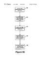
- FIG. 6 ais a flowchart illustrating one method for providing a substantially constant bandwidth in a phase-locked loop according to the present invention.
- FIG. 6 bis a flowchart illustrating another method for providing a substantially constant bandwidth in a phase-locked loop according to the present invention.
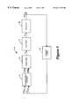
- FIG. 2depicts the components of an oscillator 40 .
- Oscillator 40is implemented in at least two stages: a voltage-to-current converter 42 and a current-controlled oscillator 42 .
- Voltage-to-current converter 42generates a control current I REF proportional to the value of an input control voltage V LF .
- the voltage V LFis typically generated by a loop filter and has an amplitude representative of necessary adjustments to the output clock frequency.
- the current I REFis applied to current-controlled oscillator 44 , which adjusts the frequency of an output clock signal CLK OUT according to the value of I REF .
- Voltage-to-current converter 42generates a control current I REF proportional to the value of control voltage V LF input to the gate of NMOS transistor M 2 .
- a resistor R 2is connected in series between the source of transistor M 2 and ground.
- resistor R 2is an integrated, temperature-variable well resistor having a temperature coefficient of approximately 5000 ppm/° C.
- Application of the loop filter voltage to the gate of transistor M 2develops a voltage V X across well resistor R 2 that can be expressed as:
- V XV LF ⁇ V T2 ;
- V T2is the gate-to-source threshold voltage of transistor M 2 .
- the control current I REFis mirrored to current-controlled oscillator 44 through a current mirror implemented by PMOS transistors M 1 and M 3 .
- the drain of transistor M 2is coupled to the drain of transistor M 1 and to the gates of both mirror transistors M 1 and M 3 .
- the sources of transistors M 1 and M 3are coupled to a supply voltage V DD .
- the control current I REF generated in the M 1 -M 2 branchis mirrored to the M 3 branch and supplied to current-controlled oscillator 44 .
- additional current mirror transistorsmay be implemented between voltage-to-current converter 42 and current-controlled oscillator 44 .
- An implementation with additional current mirrors and a cascoded configurationis set forth in U.S. patent application Ser. No. 09/xxx,xxx, filed on Apr. 30, 1999, which shares a common assignee with the present application. This application is incorporated herein by reference as thought set forth in full. The referenced application also sets forth a circuit implementation of a current-controlled oscillator that would be appropriate for use in conjunction with voltage-to-current converter 42 .
- FIG. 4A circuit implementation of a loop filter 30 according to the present invention is set forth in FIG. 4 .
- the current I CP output by a charge pump 60is input to loop filter 30 to generate a voltage V LF that is applied to oscillator 40 .
- Loop filter 30as shown, consists of a series-connected resistor R 1 and capacitor C 1 in parallel with a capacitor C 2 .
- Capacitors C 1 and C 2form an integrating capacitor. If, in response to an UP pulse from a phase detector, I CP is positive, the integrating capacitor is charged and V LF increases by an amount commensurate with the duration of the UP pulse.
- resistor R 1is a temperature-variable, integrated well resistor having a temperature coefficient in the range of 5000 ppm/° C. Moreover, the resistance of resistor R 1 is substantially equal to the resistance of resistor R 2 . As will be set forth in detail below, use of complementary resistors R 1 and R 2 in oscillator 40 and loop filter 30 having substantially equal temperature coefficients and resistances helps to maintain loop bandwidth stability over temperature variations.
- phase-locked loop 100implementing loop filter 30 and oscillator 40 as described above is depicted in FIG. 5 .
- phase-locked loop 100is integrated on a semiconductor chip with CMOS technology.
- I CP ⁇ R 1is the gain of loop filter 30
- K VCOis the frequency gain of oscillator 40
- Nis the division factor of frequency divider 70 .
- integrated well resistors R 1 and R 2have temperature coefficients of nearly 5000 ppm/° C., their resistances may vary as much as 50% over a 100° C. range. The presence of resistor R 1 in equation 1 thus raises the prospect of the loop bandwidth being very dependent on circuit temperature and hence unstable in relation to temperature variations. As the analysis below shows, however, the placement of a complementary well resistor R 2 in oscillator 40 has the effect of stabilizing the loop bandwidth.
- resistors R 1 and R 2have substantially equal temperature coefficients, variations in their resistances due to temperature fluctuations will also be substantially the same. Fluctuations in loop bandwidth due to temperature fluctuations, therefore, will be minimized.
- a decrease in the oscillator gain due to a temperature-induced increase in the resistance of R 2for example, will be substantially if not wholly compensated for by an increase in the loop filter voltage due to a corresponding temperature-induced increase in the resistance of R 1 (and vice-versa). Loop stability is maximized when resistors R 1 and R 2 have substantially equal resistances.
- FIG. 6 abroadly depicts a method for counteracting perturbations in the loop bandwidth of a phase-locked loop due to temperature fluctuations.
- a PLL having a first temperature sensitive elementis provided.
- the temperature sensitive elementis a resistor and is placed in one of the loop filter or the oscillator.
- a second temperature-sensitive elementis obtained.
- the second temperature-sensitive elementis a resistor.
- the first and second resistorsare integrated well resistors having a temperature coefficient of approximately 5000 ppm/° C.
- the second temperature-sensitive elementis situated in the PLL to stabilize the loop bandwidth during temperature fluctuations. That is, it is situated to substantially counteract perturbations in the loop bandwidth due to temperature fluctuations.
- the second temperature elementis placed in the other of the loop filter and the oscillator in a complementary relationship to the first temperature-sensitive element.
- FIG. 6 bdepicts another method for providing a substantially constant loop bandwidth in a PLL.
- a first temperature-variable resistor R 1is obtained.
- R 1is an integrated well resistor having a temperature coefficient of approximately 5000 ppm/° C.
- R 1is situated in the loop filter such that the loop filter gain is directly related to the resistance of R 1 (I CP ⁇ R 1 ).
- a second temperature-variable resistor R 2is obtained in step 254 .
- R 2is an integrated well resistor having a temperature coefficient of approximately 5000 ppm/° C. For best results, the resistances of resistors R 1 and R 2 are substantially equal.
- the loop bandwidthis determined as a product of the loop filter gain and the oscillator gain. In this manner, temperature-induced variations in the resistances of R 1 and R 2 are effectively offset.
Landscapes
- Stabilization Of Oscillater, Synchronisation, Frequency Synthesizers (AREA)
Abstract
Description


Claims (33)


Priority Applications (1)
| Application Number | Priority Date | Filing Date | Title |
|---|---|---|---|
| US09/314,898US6211743B1 (en) | 1999-05-19 | 1999-05-19 | Phase-locked loop having temperature-compensated bandwidth control |
Applications Claiming Priority (1)
| Application Number | Priority Date | Filing Date | Title |
|---|---|---|---|
| US09/314,898US6211743B1 (en) | 1999-05-19 | 1999-05-19 | Phase-locked loop having temperature-compensated bandwidth control |
Publications (1)
| Publication Number | Publication Date |
|---|---|
| US6211743B1true US6211743B1 (en) | 2001-04-03 |
Family
ID=23221961
Family Applications (1)
| Application Number | Title | Priority Date | Filing Date |
|---|---|---|---|
| US09/314,898Expired - LifetimeUS6211743B1 (en) | 1999-05-19 | 1999-05-19 | Phase-locked loop having temperature-compensated bandwidth control |
Country Status (1)
| Country | Link |
|---|---|
| US (1) | US6211743B1 (en) |
Cited By (15)
| Publication number | Priority date | Publication date | Assignee | Title |
|---|---|---|---|---|
| US20020051509A1 (en)* | 2000-09-30 | 2002-05-02 | Manfred Lindner | Phase-locked loop |
| US6389092B1 (en)* | 1999-08-11 | 2002-05-14 | Newport Communications, Inc. | Stable phase locked loop having separated pole |
| US20030235262A1 (en)* | 2002-06-19 | 2003-12-25 | Staszewski Robert B. | Fine-grained gear-shifting of a digital phase-locked loop (PLL) |
| KR100424174B1 (en)* | 2001-08-21 | 2004-03-24 | 주식회사 하이닉스반도체 | Phase locked loop circuit |
| US6731712B1 (en)* | 2000-02-04 | 2004-05-04 | Conexant Systems, Inc. | Fully integrated broadband tuner |
| US6748041B1 (en) | 1999-08-11 | 2004-06-08 | Broadcom Corporation | GM cell based control loops |
| US6779126B1 (en)* | 2000-08-31 | 2004-08-17 | Micron Technology, Inc. | Phase detector for all-digital phase locked and delay locked loops |
| US6993106B1 (en) | 1999-08-11 | 2006-01-31 | Broadcom Corporation | Fast acquisition phase locked loop using a current DAC |
| US20090085622A1 (en)* | 2007-09-27 | 2009-04-02 | Nanoamp Solutions, Inc. (Cayman) | Phase-locked loop start-up techniques |
| US8487639B1 (en)* | 2008-11-21 | 2013-07-16 | Cypress Semiconductor Corporation | Receive demodulator for capacitive sensing |
| US8866500B2 (en) | 2009-03-26 | 2014-10-21 | Cypress Semiconductor Corporation | Multi-functional capacitance sensing circuit with a current conveyor |
| US9268441B2 (en) | 2011-04-05 | 2016-02-23 | Parade Technologies, Ltd. | Active integrator for a capacitive sense array |
| US9325276B2 (en)* | 2014-03-03 | 2016-04-26 | Sandisk Technologies Inc. | Methods and apparatus for clock oscillator temperature coefficient trimming |
| US9514831B2 (en) | 2014-01-29 | 2016-12-06 | Sandisk Technologies Llc | Multi-clock generation through phase locked loop (PLL) reference |
| US10985767B2 (en)* | 2017-11-15 | 2021-04-20 | Ams Ag | Phase-locked loop circuitry having low variation transconductance design |
Citations (4)
| Publication number | Priority date | Publication date | Assignee | Title |
|---|---|---|---|---|
| US4717891A (en)* | 1985-06-25 | 1988-01-05 | Canon Kabushiki Kaisha | Phase locked loop circuit having temperature compensated VCO control voltage |
| US5426398A (en)* | 1994-08-19 | 1995-06-20 | National Semiconductor Corporation | High speed differential mode voltage controlled ring oscillator |
| US5963105A (en)* | 1997-07-31 | 1999-10-05 | Dallas Semiconductor Corporation | Trimmable circuitry for providing compensation for the temperature coefficients of a voltage controlled crystal-less oscillator |
| US6078634A (en)* | 1993-10-08 | 2000-06-20 | Texas Instruments Incorporated | Phase-locked loop circuit with a multi-cycle phase detector and multi-current charge pump |
- 1999
- 1999-05-19USUS09/314,898patent/US6211743B1/ennot_activeExpired - Lifetime
Patent Citations (4)
| Publication number | Priority date | Publication date | Assignee | Title |
|---|---|---|---|---|
| US4717891A (en)* | 1985-06-25 | 1988-01-05 | Canon Kabushiki Kaisha | Phase locked loop circuit having temperature compensated VCO control voltage |
| US6078634A (en)* | 1993-10-08 | 2000-06-20 | Texas Instruments Incorporated | Phase-locked loop circuit with a multi-cycle phase detector and multi-current charge pump |
| US5426398A (en)* | 1994-08-19 | 1995-06-20 | National Semiconductor Corporation | High speed differential mode voltage controlled ring oscillator |
| US5963105A (en)* | 1997-07-31 | 1999-10-05 | Dallas Semiconductor Corporation | Trimmable circuitry for providing compensation for the temperature coefficients of a voltage controlled crystal-less oscillator |
Non-Patent Citations (1)
| Title |
|---|
| "Design of PLL-Based Clock Generation Circuits"; IEEE Journal of Solid-State Circuits, Apr., 1987, pp. 255-261, Deog-Kyoon Jeong et al. |
Cited By (24)
| Publication number | Priority date | Publication date | Assignee | Title |
|---|---|---|---|---|
| US6389092B1 (en)* | 1999-08-11 | 2002-05-14 | Newport Communications, Inc. | Stable phase locked loop having separated pole |
| US6993106B1 (en) | 1999-08-11 | 2006-01-31 | Broadcom Corporation | Fast acquisition phase locked loop using a current DAC |
| US6748041B1 (en) | 1999-08-11 | 2004-06-08 | Broadcom Corporation | GM cell based control loops |
| US20040190669A1 (en)* | 1999-08-11 | 2004-09-30 | Broadcom Corporation | GM cell based control loops |
| US6731712B1 (en)* | 2000-02-04 | 2004-05-04 | Conexant Systems, Inc. | Fully integrated broadband tuner |
| US6987701B2 (en) | 2000-08-31 | 2006-01-17 | Micron Technology, Inc. | Phase detector for all-digital phase locked and delay locked loops |
| US7123525B2 (en) | 2000-08-31 | 2006-10-17 | Micron Technology, Inc. | Phase detector for all-digital phase locked and delay locked loops |
| US6779126B1 (en)* | 2000-08-31 | 2004-08-17 | Micron Technology, Inc. | Phase detector for all-digital phase locked and delay locked loops |
| US20040223367A1 (en)* | 2000-08-31 | 2004-11-11 | Feng Lin | Phase detector for all-digital phase locked and delay locked loops |
| US20050270893A1 (en)* | 2000-08-31 | 2005-12-08 | Feng Lin | Phase detector for all-digital phase locked and delay locked loops |
| US7020229B2 (en)* | 2000-09-30 | 2006-03-28 | Infineon Technologies Ag | Phase-locked loop |
| US20020051509A1 (en)* | 2000-09-30 | 2002-05-02 | Manfred Lindner | Phase-locked loop |
| KR100424174B1 (en)* | 2001-08-21 | 2004-03-24 | 주식회사 하이닉스반도체 | Phase locked loop circuit |
| US20030235262A1 (en)* | 2002-06-19 | 2003-12-25 | Staszewski Robert B. | Fine-grained gear-shifting of a digital phase-locked loop (PLL) |
| US8306176B2 (en)* | 2002-06-19 | 2012-11-06 | Texas Instruments Incorporated | Fine-grained gear-shifting of a digital phase-locked loop (PLL) |
| US20090085622A1 (en)* | 2007-09-27 | 2009-04-02 | Nanoamp Solutions, Inc. (Cayman) | Phase-locked loop start-up techniques |
| US7639088B2 (en) | 2007-09-27 | 2009-12-29 | Nanoamp Mobile, Inc. | Phase-locked loop start-up techniques |
| US8487639B1 (en)* | 2008-11-21 | 2013-07-16 | Cypress Semiconductor Corporation | Receive demodulator for capacitive sensing |
| US8866500B2 (en) | 2009-03-26 | 2014-10-21 | Cypress Semiconductor Corporation | Multi-functional capacitance sensing circuit with a current conveyor |
| US9442146B2 (en) | 2009-03-26 | 2016-09-13 | Parade Technologies, Ltd. | Multi-mode capacitive sensing device and method with current conveyor |
| US9268441B2 (en) | 2011-04-05 | 2016-02-23 | Parade Technologies, Ltd. | Active integrator for a capacitive sense array |
| US9514831B2 (en) | 2014-01-29 | 2016-12-06 | Sandisk Technologies Llc | Multi-clock generation through phase locked loop (PLL) reference |
| US9325276B2 (en)* | 2014-03-03 | 2016-04-26 | Sandisk Technologies Inc. | Methods and apparatus for clock oscillator temperature coefficient trimming |
| US10985767B2 (en)* | 2017-11-15 | 2021-04-20 | Ams Ag | Phase-locked loop circuitry having low variation transconductance design |
Similar Documents
| Publication | Publication Date | Title |
|---|---|---|
| US6160432A (en) | Source-switched or gate-switched charge pump having cascoded output | |
| Foley et al. | CMOS DLL-based 2-V 3.2-ps jitter 1-GHz clock synthesizer and temperature-compensated tunable oscillator | |
| US6377129B1 (en) | Programmable relaxation oscillator | |
| US6208183B1 (en) | Gated delay-locked loop for clock generation applications | |
| US6608511B1 (en) | Charge-pump phase-locked loop circuit with charge calibration | |
| EP2425533B1 (en) | Supply-regulated phase-locked loop (pll) and method of using | |
| US7646253B2 (en) | Frequency-locked clock generator | |
| US7443254B2 (en) | Relaxation oscillator with propagation delay compensation for improving the linearity and maximum frequency | |
| US7586347B1 (en) | Clock generator with self-bias bandwidth control | |
| US6211743B1 (en) | Phase-locked loop having temperature-compensated bandwidth control | |
| US8558592B2 (en) | Charge pump and active filter for a feedback circuit | |
| US5727037A (en) | System and method to reduce phase offset and phase jitter in phase-locked and delay-locked loops using self-biased circuits | |
| US10635130B2 (en) | Process, voltage and temperature tolerant clock generator | |
| US6693496B1 (en) | Method and system for low power, low jitter, wide range, self-adaptive multi-frequency phase locked loop | |
| US6900675B2 (en) | All digital PLL trimming circuit | |
| US10812090B2 (en) | Ultra-low power, real time clock generator and jitter compensation method | |
| JPH09172370A (en) | PLL circuit | |
| CN112953527B (en) | Quick locking phase-locked loop structure and electronic equipment | |
| US7268633B2 (en) | Voltage-controlled oscillator for low-voltage, wide frequency range operation | |
| CN114244350A (en) | Charge-accelerated pump and phase-locked loop and method of operating the same | |
| US20090206893A1 (en) | Charge pump circuit and pll circuit | |
| US7002382B2 (en) | Phase locked loop circuit | |
| LU500939B1 (en) | Enhanced PLL circuit | |
| KR100742016B1 (en) | Tunable Oscillator and Propagation Delay Compensation Method | |
| JP3008938B1 (en) | PLL circuit |
Legal Events
| Date | Code | Title | Description |
|---|---|---|---|
| AS | Assignment | Owner name:CONEXANT SYSTEMS, INC., CALIFORNIA Free format text:CORRECTIVE ASSIGNMENT TO CORRECT SERIAL NUMBER 09/314,890 THAT WAS PREVIOUSLY RECORDED ON REEL 10140, FRAME 0544;ASSIGNORS:RHEE, WOOGEUN;CONTA, MATTEO;ALI, AKBAR;REEL/FRAME:010379/0184 Effective date:19990716 | |
| AS | Assignment | Owner name:CREDIT SUISSE FIRST BOSTON, NEW YORK Free format text:SECURITY INTEREST;ASSIGNOR:CONEXANT SYSTEMS, INC.;REEL/FRAME:010450/0899 Effective date:19981221 | |
| STCF | Information on status: patent grant | Free format text:PATENTED CASE | |
| AS | Assignment | Owner name:CONEXANT SYSTEMS, INC., CALIFORNIA Free format text:RELEASE OF SECURITY INTEREST;ASSIGNOR:CREDIT SUISSE FIRST BOSTON;REEL/FRAME:012252/0865 Effective date:20011018 Owner name:BROOKTREE CORPORATION, CALIFORNIA Free format text:RELEASE OF SECURITY INTEREST;ASSIGNOR:CREDIT SUISSE FIRST BOSTON;REEL/FRAME:012252/0865 Effective date:20011018 Owner name:BROOKTREE WORLDWIDE SALES CORPORATION, CALIFORNIA Free format text:RELEASE OF SECURITY INTEREST;ASSIGNOR:CREDIT SUISSE FIRST BOSTON;REEL/FRAME:012252/0865 Effective date:20011018 Owner name:CONEXANT SYSTEMS WORLDWIDE, INC., CALIFORNIA Free format text:RELEASE OF SECURITY INTEREST;ASSIGNOR:CREDIT SUISSE FIRST BOSTON;REEL/FRAME:012252/0865 Effective date:20011018 | |
| AS | Assignment | Owner name:ALPHA INDUSTRIES, INC., MASSACHUSETTS Free format text:MERGER;ASSIGNOR:WASHINGTON SUB, INC.;REEL/FRAME:013253/0738 Effective date:20020625 Owner name:SKYWORKS SOLUTIONS, INC., CALIFORNIA Free format text:MERGER;ASSIGNOR:ALPHA INDUSTRIES, INC.;REEL/FRAME:013254/0265 Effective date:20020625 Owner name:WASHINGTON SUB, INC., CALIFORNIA Free format text:ASSIGNMENT OF ASSIGNORS INTEREST;ASSIGNOR:CONEXANT SYSTEMS, INC.;REEL/FRAME:013254/0311 Effective date:20020625 | |
| AS | Assignment | Owner name:CONEXANT SYSTEMS, INC., CALIFORNIA Free format text:SECURITY INTEREST;ASSIGNOR:ALPHA INDUSTRIES, INC.;REEL/FRAME:013240/0860 Effective date:20020625 | |
| AS | Assignment | Owner name:SKYWORKS SOLUTIONS, INC., CALIFORNIA Free format text:MERGER;ASSIGNOR:ALPHA INDUSTRIES, INC.;REEL/FRAME:013362/0869 Effective date:20020625 Owner name:WASHINGTON SUB, INC., CALIFORNIA Free format text:ASSIGNMENT OF ASSIGNORS INTEREST;ASSIGNOR:CONEXANT SYSTEMS, INC.;REEL/FRAME:013342/0049 Effective date:20020625 Owner name:ALPHA INDUSTRIES, INC., MASSACHUSETTS Free format text:MERGER;ASSIGNOR:WASHINGTON SUB, INC.;REEL/FRAME:013368/0467 Effective date:20020625 | |
| AS | Assignment | Owner name:ALPHA INDUSTRIES, INC., MASSACHUSETTS Free format text:RELEASE AND RECONVEYANCE/SECURITY INTEREST;ASSIGNOR:CONEXANT SYSTEMS, INC.;REEL/FRAME:014580/0880 Effective date:20030307 | |
| FPAY | Fee payment | Year of fee payment:4 | |
| FPAY | Fee payment | Year of fee payment:8 | |
| FPAY | Fee payment | Year of fee payment:12 |