US6211738B1 - Stability and enhanced gain of amplifiers using inductive coupling - Google Patents
Stability and enhanced gain of amplifiers using inductive couplingDownload PDFInfo
- Publication number
- US6211738B1 US6211738B1US09/016,195US1619598AUS6211738B1US 6211738 B1US6211738 B1US 6211738B1US 1619598 AUS1619598 AUS 1619598AUS 6211738 B1US6211738 B1US 6211738B1
- Authority
- US
- United States
- Prior art keywords
- amplifier
- inductor
- feedback
- mutual inductance
- input
- Prior art date
- Legal status (The legal status is an assumption and is not a legal conclusion. Google has not performed a legal analysis and makes no representation as to the accuracy of the status listed.)
- Expired - Lifetime
Links
Images


Classifications
- H—ELECTRICITY
- H03—ELECTRONIC CIRCUITRY
- H03F—AMPLIFIERS
- H03F1/00—Details of amplifiers with only discharge tubes, only semiconductor devices or only unspecified devices as amplifying elements
- H03F1/34—Negative-feedback-circuit arrangements with or without positive feedback
- H03F1/347—Negative-feedback-circuit arrangements with or without positive feedback using transformers
- H—ELECTRICITY
- H03—ELECTRONIC CIRCUITRY
- H03F—AMPLIFIERS
- H03F1/00—Details of amplifiers with only discharge tubes, only semiconductor devices or only unspecified devices as amplifying elements
- H03F1/08—Modifications of amplifiers to reduce detrimental influences of internal impedances of amplifying elements
- H03F1/14—Modifications of amplifiers to reduce detrimental influences of internal impedances of amplifying elements by use of neutralising means
Definitions
- the inventionrelates to minimizing feedback in transistor amplifiers. More specifically, the invention uses inductive coupling to cancel a portion of the feedback inherent in these amplifiers.
- Amplifiersare subject to reduced gain when feedback between the input and output signals occurs.
- Conventional transistor amplifiersare especially subject to instability from feedback. Such feedback is inherent in transistors due to the presence of parasitic and junction capacitance between the collector-base or the drain-gate terminals.
- a handsetin a cordless telephone system, a handset generates, amplifies and then transmits the signals to a base station. Any instability or decrease in gain of the amplifier, however, may decrease the quality of the transmitted signal, and as a result, can decrease the performance of the telephone system.
- an inductive elementbetween the output and the input terminals can reduce the amount of amplifier feedback at specific frequencies.
- the presence of the inductive elementcreates a parallel resonant circuit with the feedback capacitance which presents a high impedance feedback path at the resonant frequency. This technique is known as neutralization.
- a neutralized amplifierwill demonstrate improved stability and increased gain because of the reduction of capacitive feedback.
- the present inventionprovides a unique apparatus and method which improves stability and enhances gain of an amplifier by using mutual inductance to resonate with the feedback capacitance.
- an amplifieramplifies signals prior to transmission to a base station. These amplifiers, however, are subject to reduced performance due to capacitive feedback.
- the present inventionminimizes the capacitive feedback through the use of mutually coupled inductors. Previously, neutralization was accomplished with a single physical inductor. Using mutual inductance to resonate with the feedback capacitance allows the physical inductor element to be eliminated.
- One embodiment of the inventionpositions these inductors near each other so to create a mutual inductance between the two inductors. This mutual inductance couples the output terminal to the input terminal of the amplifier. The mutual inductance resonates with the feedback capacitance and thus minimizes the feedback of the amplifier at the resonant frequency.
- Coupled inductorsto neutralize the amplifier also reduces the problem of low-frequency instability. Coupling between inductors decreases at low frequencies. If a mutual inductance is used in the feedback path, this feedback will decrease as the frequency is reduced. Stability of the amplifier is a concern at lower frequencies because the transistor exhibits more gain at lower frequencies. Therefore, the use of a mutual inductance tends to reduce the feedback in the range of frequencies where the gain is greatest, and thus the operation of the amplifier is more stable. By contrast, a discrete inductor between the output and input terminals of the amplifier results in more feedback at lower frequencies, and the operation of the amplifier in this region is less stable.
- Another advantage of using coupled inductorsis that large values of effective inductance may be realized by choosing an appropriately small value of mutual inductance. In many cases, the value of the inductive element needed to neutralize the amplifier is relatively large. The large value required often makes the use of a discrete inductor unfeasible. This is especially true in integrated circuit amplifiers where the size of each component is critical.
- Another advantage of the inventionis the ability to use relatively small inductors. Using a small amount of mutual inductance causes a large value of inductance to be sensed across the feedback path. Because the physical proximity of the coupled inductors can control the amount of mutual inductance, inductors with small values can maintain a large value of inductance sensed across the feedback path.
- MMIC amplifiersare a type of semiconductor amplifier used in the telephone industry.
- printed elementssuch as spiral inductors are generally tolerant to process and temperature changes. This allows the amount of coupling to be precisely controlled once the layout of the circuit is fixed.
- One embodiment of the inventionexploits components which may already exist in an amplifier circuit to minimize the capacitive feedback. This allows the amplifier to be neutralized without any increase in cost of manufacturing.
- One embodiment of the present inventionis a telephone handset for communicating with a base station.
- the handsetgenerates and amplifies signals to be transmitted to the base station.
- the handsetcomprises an amplifier for boosting the gain of the signals prior to transmission, the amplifier having capacitive feedback between an input and an output of the transistor wherein a mutual inductance neutralizes the amplifier.
- the amplifiercomprises a transistor having an input terminal and an output terminal, a first inductor coupled to the input terminal of the transistor, and a second inductor coupled to the output terminal of the transistor.
- the first inductor and the second inductorare positioned relative to each other to create the mutual inductance between the output terminal of the transistor and the input terminal of the transistor, the mutual inductance resonating with the feedback capacitance in the transistor.
- the amplifier, the first inductor, and the second inductorare implemented on an integrated circuit without the use of discrete components.
- Another embodiment of the present inventionis an apparatus comprising an amplifier having an input terminal and an output terminal.
- a first inductoris coupled to the input terminal of the amplifier and a second inductor is coupled to the output terminal of the amplifier.
- the first inductor and the second inductorare positioned relative to each other to create a mutual inductance which cancels at least a portion of feedback in the amplifier.
- the mutual inductanceis created between the output terminal of the amplifier and the input terminal of the amplifier.
- the mutual inductanceresonates with the feedback capacitance in the amplifier.
- the amplifier, the first inductor, and the second inductormay be implemented on a semiconductor material without the use of discrete components.
- a further embodiment of the present inventionis a method of reducing feedback in an amplifier.
- the methodcomprises the acts of coupling a first inductor to an input terminal of the amplifier and coupling a second inductor to an output terminal of the amplifier.
- the first inductor and the second inductorare then positioned relative to each other to create a mutual inductance which cancels at least a portion of the feedback in the amplifier.
- An additional embodiment of the present inventionis an apparatus comprising means for amplifying a signal having an input and an output.
- a first inductive meansis coupled to the input of the amplifying means.
- a second inductive meansis coupled to the output of the amplifying means.
- the first inductive means and the second inductive meansare positioned relative to each other to create a mutual inductance between the output of the amplifying means and the input of the amplifying means, the mutual inductance neutralizing the amplifying means.
- FIG. 1is a block diagram of a cordless telephone system appropriate for use with the present invention.
- FIG. 2is a block diagram of an amplifier which uses an inductor to neutralize the amplifier.
- FIG. 3is a schematic diagram of a transistor amplifier which uses inductive coupling to neutralize the amplifier.
- FIG. 4 ais a schematic diagram of the mutual inductance of the transistor amplifier of FIG. 3 .
- FIG. 4 bis a schematic diagram of an electrically equivalent circuit of the circuit in FIG. 4 a.
- FIG. 5 aillustrates the feedback of an amplifier without any neutralization.
- FIG. 5 billustrates the feedback of an amplifier which uses an inductor to resonate with the feedback capacitance.
- FIG. 5 cillustrates the feedback of an amplifier which uses inductive coupling to resonate with the feedback capacitance.
- FIG. 6 aillustrates the overall gain performance of an amplifier in which neutralization is accomplished with inductive coupling.
- FIG. 6 billustrates the overall feedback of an amplifier in which neutralization is accomplished with inductive coupling.
- FIG. 1A telephone system 100 appropriate for use with one embodiment of the invention is illustrated in FIG. 1 .
- the telephone system 100includes a handset 105 and a base station 110 .
- a userspeaks into a microphone 115 on the handset 105 .
- a signal generator 120converts the voice detected by the microphone 115 into a signal 122 .
- the signal 122is input into an amplifier circuit 125 to enhance the range of the handset 105 .
- the amplifier circuit 125outputs an amplified signal 127 which is sent to an antenna 135 for transmission to the base station 110 .
- the amplified signal 127is transmitted as indicated by line 140 , to an antenna 145 located on the base station 110 .
- the handset 105 and the base station 110can be either part of a cordless telephone system, a cellular telephone system, or the like.
- FIG. 2One embodiment of the amplifier circuit 125 which may exist in the telephone system 100 is shown in FIG. 2 .
- an input signal 205is fed into the input of an amplifier 200 and after amplification, an output signal 210 results.
- the amplifier 200may contain a capacitive feedback path 215 connecting the output signal 210 to the input signal 205 .
- the amount of feedback capacitance presentis indicated by a capacitor C 1 in the capacitive feedback path 215 .
- the capacitor C 1is not a physical capacitor but merely the capacitive feedback component of the amplifier 200 .
- an inductive path 220may be added in parallel with the capacitive feedback path 215 to neutralize the amplifier 200 .
- the inductive path 220contains a physical inductor L n .
- the use of a physical inductor L ndecreases the total feedback along the feedback path 211 at the resonant frequency of the inductor-capacitor combination which comprises the inductor L n and the inherent feedback capacitance C 1 .
- the use of the physical inductor L nalso presents many disadvantages.
- the inductor L nprovides a low impedance feedback path 211 . This low impedance at lower frequencies increases the amount of feedback and results in stability problems in this region.
- the actual value of the inductor L n required to resonate with the capacitive feedbackis often quite large. This large value of inductance is usually prohibitive in a integrated circuit environment.
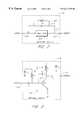
- FIG. 3One embodiment of the amplifier circuit 125 comprising a transistor amplifier 300 using inductive coupling to resonate with the feedback capacitor is shown FIG. 3 .
- the transistor amplifier 300contains capacitors C 2 and C 3 , a transistor Q 1 , and inductors L 1 and L 2 .
- Power sources V b and V care provided for the transistor Q 1 .
- the presence of the inherent feedback between the collector and the baseis indicated in shadow by a capacitor C f .
- the feedback current from the output of the transistor Q 1 to the input of the transistor Q 1is indicated by a current I f .
- the transistor amplifier 300receives an input signal 305 .
- the input signal 305is coupled to a first terminal of the capacitor C 2 .
- the second terminal of the capacitor C 2is connected to the first terminal of the inductor L 1 and a base of the transistor Q 1 .
- the second terminal of the inductor L 1is connected to a first terminal of a power source V b .
- the second terminal of the power source V bis connected to ground.
- the base of the transistor Q 1is also connected to the capacitive feedback path represented by the capacitor C f .
- the emitter of the transistor Q 1is connected to ground.
- the collector of the transistor Q 1is connected to a first terminal of the capacitor C 3 , a first terminal of the inductor L 2 and the second terminal of the capacitive feedback path represented by the capacitor C f .
- the second terminal of capacitor C 3is connected as the output signal 310 .
- the second terminal of the inductor L 2is connected to a first terminal of a power source V c .
- the second terminal of the power source V cis connected to ground.
- the inductors L 1 and L 2are physically positioned so as to create a mutual inductance M between the inductors L 1 and L 2 .
- the mutual inductance Mappears across the collector base junction of the transistor Q 1 .
- the inductor L 1 in combination with the capacitor C 2tune the input of the amplifier 300 and the inductor L 2 in combination with the capacitor C 3 tune the output of the amplifier 300 .
- the inductor L 2provides a DC path for the power supply V c to power the transistor Q 1 .
- the inductor L 1also provides bias to the base of the transistor Q 1 .
- positioning the inductors L 1 and L 2 to create a mutual inductance Mdoes not effect each independent inductor's role in either tuning or providing the DC path.
- the mutual inductance Mis in parallel with the capacitive feedback path represented by the capacitor C f . Because the mutual inductance M is in parallel with the capacitive feedback path C f , the amount of feedback at the resonant frequency is minimized.
- FIG. 4 aillustrates an inductive coupled circuit 400 utilizing the two inductors L 1 and L 2 coupled by a mutual inductance of M.
- a signal V 1creates a current represented by I 1 .
- I 1the current flowing through the inductor L 1
- the mutual coupling between inductors L 1 and L 2creates a current I 2 which flows through the indicated load resistor R L in the inductive coupled circuit 400 .
- the inductive coupled circuit 400can be redrawn conceptually as a pi network circuit 410 as indicated in FIG. 4 b.
- the inductors L 1 and L 2 along with the mutual inductance Mcan be represented by three separate inductors. The values of these three inductors are dependent upon the value of the inductors L 1 and L 2 and the value of the mutual inductance M coupling the inductors L 1 and L 2 .
- the signal V 1is connected to a first terminal of a first inductor L′ 1 and a first terminal of a second inductor M′.
- the second terminal of the inductor M′is connected to a first terminal of the inductor L′ 2 and a first terminal of the load resistance R L .
- the second terminal of the source signal V 1is connected to the second terminal of the inductor L′ 1 , the second terminal of the inductor L′ 2 , and the second terminal of the load resistance R L .
- the values of the inductors L′ 1 , L′ 2 and M′vary dependent upon the values chosen for the inductors L 1 , L 2 , and the mutual inductance M in FIG. 4 a.
- L′ 2L 1 ⁇ L 2 - M 2 L 1 - M
- M′L 1 ⁇ L 2 - M 2 M
- HBTheterojunction bipolar transistor
- MOSFETmetal-oxide-semiconductor field-effect transistors
- CMOScomplementary metal-oxide-semiconductor transistors
- spiral inductors L 1 and L 2are used. As is known to one of skill in the art, spiral inductors L 1 and L 2 are printed directly on the integrated circuit substrate. By printing the spiral inductors L 1 and L 2 directly on the integrated circuit, the physical location is permanently fixed and therefore determines the value of the mutual inductance M. Determination of the proper placement of the spiral inductors L 1 and L 2 to create the desired mutual inductance M may be achieved by testing or computer simulation. Although spiral inductors may be used, the inductors L 1 and L 2 are not limited to spiral inductors and can be of any type compatible for use with an integrated circuit.
- the amplifier circuit 125exists in a cordless telephone system with a desired frequency of operation at 1.9 gigahertz (GHz).
- the amplifier circuitis part of a MMIC amplifier using an HBT formed on a gallium arsenide substrate.
- the HBT device usedhas a collector-base feedback capacitance (junction and parasitic) of approximately 0.4 picofarad (pF).
- the equivalent inductance needed to resonate with this capacitanceis 17.5 nanohenry (nH).
- a printed spiral inductor of 17.5 nHwould generally require a large amount of die space on the integrated circuit, and would be cost prohibitive.
- relatively small value spiral inductors L 1 and L 2can generate a relatively large effective inductance which is sensed across the feedback path.
- two shunt inductorsare currently required at the base and the collector of the device for matching and bias purposes. These inductors may be repositioned to create the mutual inductance M. This allows the present invention to be implemented on an integrated circuit without adding any elements to the circuit.
- wireless telephone systemsoperate at frequencies of about 800 megahertz (MHz) and above.
- the systemoperates in a frequency range from about 800 MHz to about 2.5 GHz.
- the frequency rangecan be from about 900 MHz to about 2 GHz, and more precisely from about 1.3 MHz to 1.9 GHz.
- PHSPersonal Handy Phone System
- the wireless frequencyoperates at about 1.9 GHz.
- These high frequency rangesrequire inductor values to be relatively small. The use of mutual inductance allows the relatively small physical inductors needed at these high frequencies yet provides a large effective inductance needed to neutralize the amplifier. This is because of the relationship between the value of the inductors and the value of the mutual inductance M discussed above.
- FIGS. 5 a - 5 cillustrate the amount of feedback present in relation to the frequency in three different embodiments.
- the amount of feedback present in an amplifier circuitis charted in relation to the frequency of operation.
- the feedbackis measured from ⁇ 20 to 0 dB and the frequency ranges from 10 Mhz to 10 GHz.
- FIG. 5 aillustrates the amount of feedback without neutralization.
- the feedbackis low, but the feedback rapidly increases as the frequency increases.
- This feedback relationshipis shown by the portion of the curve 505 .
- the target frequency F tis a desired frequency of operation.
- the target frequency F tmay be a single frequency or a range of frequencies. In a cordless or cellular telephone system, the target frequency ranges from about 800 MHz to about 2.5 GHz.
- the amount of feedback present at the target frequency F tis shown on the feedback curve as item 500 .
- the amount of feedback present at the target frequency F tis high, and could reduce the stability of the transistor amplifier.
- the amount of feedbackalso increases as shown by the portion of the curve 510 .
- the amount of feedback on the portion of the curve 510may prevent stable operation of the amplifier at a high frequency.
- FIG. 5 bThe effect of placing a physical inductor L n in parallel with the capacitive feedback path is shown in FIG. 5 b.
- a circuit representative of the feedback performance illustrated in FIG. 5 bis shown in FIG. 2 .
- the feedback at the target frequency F tis minimized as indicated by the dip in the curve 522 .
- the physical inductor L nbegins to present a low impedance feedback path. This causes the amount of feedback to rapidly increase as the frequency decreases from the target frequency F t as indicated by a path 520 .
- FIG. 5 billustrates that placing a physical inductor L n in parallel with the capacitive feedback path works at a specific target frequency F t , but actually may decrease the stability performance of the amplifier at frequencies below the target frequency F t .
- the feedback response of the mutually coupled inductive transistor amplifier 300 of FIG. 3is shown in FIG. 5 c.
- the feedbackis minimized at the target frequency F t as indicated by the trough 535 of the curve.
- the reduction of feedback in the transistor amplifier 300allows the amplifier to operate with maximum gain and maximum stability.
- the mutually coupled inductance at this single frequencyoperates as if it is the physical inductor L n .
- the amount of feedbackslowly increases as indicated by a peak 540 . This is similar to the operation shown in FIG. 5 b, when the frequency of operation varies from the resonant frequency. However, the amount of feedback at the lower frequencies is still low.
- the mutual inductance Malso begins to decrease. This causes the amount of feedback to decrease as indicated by a curve 542 . This further decrease in feedback allows the transistor amplifier 300 to operate at low frequencies in a stable region. Increasing the frequency above the target frequency F t increases the amount of feedback as shown by a curve 545 . Depending on the gain of the amplifier, the increased frequency may cause the feedback to exceed a point at which the amplifier no longer operates in a stable region.
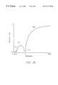
- FIG. 6 a and 6 bThe relationship between the gain of the amplifier and the total feedback is shown in FIG. 6 a and 6 b.
- the gain of a transistor amplifieris measured from 0 to 25 dB and the frequency ranges from 900 MHz to 2.9 GHz.
- the overall gain performance of a transistor amplifieris illustrated by a curve 605 .
- the gainslowly increases as the frequency increases until reaching the target frequency F t and maximum gain illustrated at a point 610 on the curve 605 .
- the amount of gainslowly decreases.
- the overall feedback component of the transistor amplifieris illustrated by a curve 630 of FIG. 6 b.
- the feedbackis measured from ⁇ 50 to 0 dB and the frequency ranges from 900 Mhz to 2.9 GHz.
- the overall feedbackslowly decreases until the target frequency F t is reached.
- the amount of feedbackis minimized as indicated by a point 635 on the curve 630 . It can be appreciated that at approximately the target frequency F t , the maximum gain at the point 610 on the curve 605 corresponding to the minimum feedback at the point 635 on the curve 630 are present.
- Increasing the frequency beyond the target frequencyslowly increases the amount of feedback as indicated the curve 630 of FIG. 6 b.
Landscapes
- Engineering & Computer Science (AREA)
- Power Engineering (AREA)
- Amplifiers (AREA)
Abstract
Description


Claims (39)
Priority Applications (2)
| Application Number | Priority Date | Filing Date | Title |
|---|---|---|---|
| US09/016,195US6211738B1 (en) | 1998-01-30 | 1998-01-30 | Stability and enhanced gain of amplifiers using inductive coupling |
| US09/783,339US20010019290A1 (en) | 1998-01-30 | 2001-02-14 | Stability and enhanced gain of amplifiers using inductive coupling |
Applications Claiming Priority (1)
| Application Number | Priority Date | Filing Date | Title |
|---|---|---|---|
| US09/016,195US6211738B1 (en) | 1998-01-30 | 1998-01-30 | Stability and enhanced gain of amplifiers using inductive coupling |
Related Child Applications (1)
| Application Number | Title | Priority Date | Filing Date |
|---|---|---|---|
| US09/783,339ContinuationUS20010019290A1 (en) | 1998-01-30 | 2001-02-14 | Stability and enhanced gain of amplifiers using inductive coupling |
Publications (1)
| Publication Number | Publication Date |
|---|---|
| US6211738B1true US6211738B1 (en) | 2001-04-03 |
Family
ID=21775882
Family Applications (2)
| Application Number | Title | Priority Date | Filing Date |
|---|---|---|---|
| US09/016,195Expired - LifetimeUS6211738B1 (en) | 1998-01-30 | 1998-01-30 | Stability and enhanced gain of amplifiers using inductive coupling |
| US09/783,339AbandonedUS20010019290A1 (en) | 1998-01-30 | 2001-02-14 | Stability and enhanced gain of amplifiers using inductive coupling |
Family Applications After (1)
| Application Number | Title | Priority Date | Filing Date |
|---|---|---|---|
| US09/783,339AbandonedUS20010019290A1 (en) | 1998-01-30 | 2001-02-14 | Stability and enhanced gain of amplifiers using inductive coupling |
Country Status (1)
| Country | Link |
|---|---|
| US (2) | US6211738B1 (en) |
Cited By (23)
| Publication number | Priority date | Publication date | Assignee | Title |
|---|---|---|---|---|
| US6531929B2 (en)* | 1998-11-23 | 2003-03-11 | Micron Technology, Inc. | Monolithic integrated circuit oscillators, complementary metal oxide semiconductor (cmos) voltage-controlled oscillators, integrated circuit oscillators, oscillator-forming methods, and oscillation methods |
| US6573797B2 (en)* | 1999-09-30 | 2003-06-03 | Fujitsu Limited | High-frequency power amplifier |
| US6593201B2 (en)* | 1998-10-26 | 2003-07-15 | Micron Technology, Inc. | Monolithic inductance-enhancing integrated circuits, complementary metal oxide semiconductor (CMOS) inductance-enhancing integrated circuits, inductor assemblies, and inductance-multiplying methods |
| US20030155977A1 (en)* | 2001-06-06 | 2003-08-21 | Johnson Douglas M. | Gain block with stable internal bias from low-voltage power supply |
| US20040085137A1 (en)* | 2002-08-27 | 2004-05-06 | Furst Claus Erdmann | Preamplifier for two terminal electret condenser microphones |
| US6753734B2 (en) | 2001-06-06 | 2004-06-22 | Anadigics, Inc. | Multi-mode amplifier bias circuit |
| WO2004086608A1 (en)* | 2003-03-28 | 2004-10-07 | Koninklijke Philips Electronics N.V. | Neutralization of feedback capacitance in amplifiers |
| US20040214434A1 (en)* | 2001-04-17 | 2004-10-28 | Atwater Harry A. | Wafer bonded virtual substrate and method for forming the same |
| US20050026432A1 (en)* | 2001-04-17 | 2005-02-03 | Atwater Harry A. | Wafer bonded epitaxial templates for silicon heterostructures |
| US20080068077A1 (en)* | 2006-09-19 | 2008-03-20 | Zuo-Min Tsai | Unilateral Feedback Power Amplifier and Method for Realizing the Same |
| US20080211061A1 (en)* | 2004-04-21 | 2008-09-04 | California Institute Of Technology | Method For the Fabrication of GaAs/Si and Related Wafer Bonded Virtual Substrates |
| US20090021295A1 (en)* | 2007-07-19 | 2009-01-22 | Chang-Tsung Fu | Dual reactive shunt low noise amplifier |
| US20090096068A1 (en)* | 2007-10-12 | 2009-04-16 | Johan Sjoestroem | System and Method for Stabilizing an Amplifier |
| JP2012191600A (en)* | 2011-02-24 | 2012-10-04 | Fujitsu Ltd | Amplifier circuit |
| EP2624448A1 (en)* | 2012-02-01 | 2013-08-07 | Telefonaktiebolaget L M Ericsson AB (Publ) | Low-noise amplifier |
| US20140203849A1 (en)* | 2011-08-12 | 2014-07-24 | E2V Technologies (Uk) Limited | Drive circuit and method for a gated semiconductor switching device |
| WO2014145623A1 (en)* | 2013-03-15 | 2014-09-18 | Rf Micro Devices, Inc. | Transformer-based power amplifier stabilization and reference distortion reduction |
| JP2015095895A (en)* | 2013-11-12 | 2015-05-18 | エフシーアイ インク | Feedback amplifier using differential inductor |
| US9413301B2 (en) | 2012-02-01 | 2016-08-09 | Telefonaktiebolaget Lm Ericsson (Publ) | Noise canceling low-noise amplifier |
| US9716470B2 (en) | 2015-05-21 | 2017-07-25 | Analog Devices, Inc. | Apparatus and methods for compensating an operational amplifier |
| EP3078115A4 (en)* | 2013-09-30 | 2017-07-26 | Texas Instruments Incorporated | Method and circuitry for multi-stage amplification |
| CN110021583A (en)* | 2017-12-22 | 2019-07-16 | 英飞凌科技股份有限公司 | Compensation equipment for transistor |
| US10498296B2 (en) | 2017-03-20 | 2019-12-03 | Texas Instruments Incorporated | Differential amplifier with variable neutralization |
Families Citing this family (4)
| Publication number | Priority date | Publication date | Assignee | Title |
|---|---|---|---|---|
| JP2005201716A (en)* | 2004-01-14 | 2005-07-28 | Honda Motor Co Ltd | Current detection device and power storage device control device |
| JP3108714U (en)* | 2004-11-11 | 2005-04-28 | アルプス電気株式会社 | Intermediate frequency circuit of television tuner |
| US12424976B2 (en) | 2021-02-09 | 2025-09-23 | QuantalRF AG | System and method for adjusting amplifier bias current based on input signal envelope tracking |
| CN116941180A (en)* | 2021-02-09 | 2023-10-24 | 量子射频股份公司 | System and method for adjusting amplifier bias current based on input signal envelope tracking |
Citations (8)
| Publication number | Priority date | Publication date | Assignee | Title |
|---|---|---|---|---|
| US3714462A (en) | 1971-06-14 | 1973-01-30 | D Blackmer | Multiplier circuits |
| US3801933A (en) | 1972-04-17 | 1974-04-02 | Rca Ltd | Low noise detector amplifier |
| US3919656A (en) | 1973-04-23 | 1975-11-11 | Nathan O Sokal | High-efficiency tuned switching power amplifier |
| US4443773A (en) | 1981-01-22 | 1984-04-17 | Licentia Patent-Verwaltungs-Gmbh | Switching network for megahertz frequency signals |
| US4588959A (en) | 1984-07-12 | 1986-05-13 | Harris Corporation | Hum neutralization circuit |
| US4692712A (en) | 1986-10-14 | 1987-09-08 | Tektronix, Inc. | Differential impedance neutralization circuit |
| US5548248A (en)* | 1995-07-30 | 1996-08-20 | Wang; Nan L. L. | RF amplifier circuit |
| US5663570A (en)* | 1993-07-12 | 1997-09-02 | Peregrine Semiconductor Corporation | High-frequency wireless communication system on a single ultrathin silicon on sapphire chip |
- 1998
- 1998-01-30USUS09/016,195patent/US6211738B1/ennot_activeExpired - Lifetime
- 2001
- 2001-02-14USUS09/783,339patent/US20010019290A1/ennot_activeAbandoned
Patent Citations (8)
| Publication number | Priority date | Publication date | Assignee | Title |
|---|---|---|---|---|
| US3714462A (en) | 1971-06-14 | 1973-01-30 | D Blackmer | Multiplier circuits |
| US3801933A (en) | 1972-04-17 | 1974-04-02 | Rca Ltd | Low noise detector amplifier |
| US3919656A (en) | 1973-04-23 | 1975-11-11 | Nathan O Sokal | High-efficiency tuned switching power amplifier |
| US4443773A (en) | 1981-01-22 | 1984-04-17 | Licentia Patent-Verwaltungs-Gmbh | Switching network for megahertz frequency signals |
| US4588959A (en) | 1984-07-12 | 1986-05-13 | Harris Corporation | Hum neutralization circuit |
| US4692712A (en) | 1986-10-14 | 1987-09-08 | Tektronix, Inc. | Differential impedance neutralization circuit |
| US5663570A (en)* | 1993-07-12 | 1997-09-02 | Peregrine Semiconductor Corporation | High-frequency wireless communication system on a single ultrathin silicon on sapphire chip |
| US5548248A (en)* | 1995-07-30 | 1996-08-20 | Wang; Nan L. L. | RF amplifier circuit |
Non-Patent Citations (2)
| Title |
|---|
| "The Radio Amateur's Handbook" 28th Edition 1951 p. 150.* |
| Anderson et al. "An Automatic Tuning and Neutralization Technique for Semiconductor Devices" ISSCC (International Solid-State Circuits Conference) Univ. of Pennsylvania, Feb. 19, 1964. pp 34-35.* |
Cited By (42)
| Publication number | Priority date | Publication date | Assignee | Title |
|---|---|---|---|---|
| US6593201B2 (en)* | 1998-10-26 | 2003-07-15 | Micron Technology, Inc. | Monolithic inductance-enhancing integrated circuits, complementary metal oxide semiconductor (CMOS) inductance-enhancing integrated circuits, inductor assemblies, and inductance-multiplying methods |
| US6680518B2 (en) | 1998-10-26 | 2004-01-20 | Micron Technology, Inc. | Monolithic inductance-enhancing integrated circuits, complementary metal oxide semiconductor (CMOS) inductance-enhancing integrated circuits, inductor assemblies, and inductance-multiplying methods |
| US6531929B2 (en)* | 1998-11-23 | 2003-03-11 | Micron Technology, Inc. | Monolithic integrated circuit oscillators, complementary metal oxide semiconductor (cmos) voltage-controlled oscillators, integrated circuit oscillators, oscillator-forming methods, and oscillation methods |
| US6573797B2 (en)* | 1999-09-30 | 2003-06-03 | Fujitsu Limited | High-frequency power amplifier |
| US7238622B2 (en) | 2001-04-17 | 2007-07-03 | California Institute Of Technology | Wafer bonded virtual substrate and method for forming the same |
| US20040214434A1 (en)* | 2001-04-17 | 2004-10-28 | Atwater Harry A. | Wafer bonded virtual substrate and method for forming the same |
| US20050026432A1 (en)* | 2001-04-17 | 2005-02-03 | Atwater Harry A. | Wafer bonded epitaxial templates for silicon heterostructures |
| US20030155977A1 (en)* | 2001-06-06 | 2003-08-21 | Johnson Douglas M. | Gain block with stable internal bias from low-voltage power supply |
| US6753734B2 (en) | 2001-06-06 | 2004-06-22 | Anadigics, Inc. | Multi-mode amplifier bias circuit |
| US6842075B2 (en) | 2001-06-06 | 2005-01-11 | Anadigics, Inc. | Gain block with stable internal bias from low-voltage power supply |
| US20040085137A1 (en)* | 2002-08-27 | 2004-05-06 | Furst Claus Erdmann | Preamplifier for two terminal electret condenser microphones |
| US6888408B2 (en)* | 2002-08-27 | 2005-05-03 | Sonion Tech A/S | Preamplifier for two terminal electret condenser microphones |
| CN1765048B (en)* | 2003-03-28 | 2010-05-05 | Nxp股份有限公司 | Neutralization of feedback capacitance in amplifiers |
| JP2006521748A (en)* | 2003-03-28 | 2006-09-21 | コーニンクレッカ フィリップス エレクトロニクス エヌ ヴィ | Neutralization of feedback capacitance in amplifiers. |
| WO2004086608A1 (en)* | 2003-03-28 | 2004-10-07 | Koninklijke Philips Electronics N.V. | Neutralization of feedback capacitance in amplifiers |
| US20080211061A1 (en)* | 2004-04-21 | 2008-09-04 | California Institute Of Technology | Method For the Fabrication of GaAs/Si and Related Wafer Bonded Virtual Substrates |
| US20080068077A1 (en)* | 2006-09-19 | 2008-03-20 | Zuo-Min Tsai | Unilateral Feedback Power Amplifier and Method for Realizing the Same |
| US7439802B2 (en)* | 2006-09-19 | 2008-10-21 | National Taiwan University | Unilateral feedback power amplifier and method for realizing the same |
| US20090009255A1 (en)* | 2006-09-19 | 2009-01-08 | Semiconductor Energy Laboratory Co., Ltd. | Unilateral feedback power amplifier and method for realizing the same |
| US7733173B2 (en)* | 2006-09-19 | 2010-06-08 | National Taiwan University | Unilateral feedback power amplifier and method for realizing the same |
| US20090021295A1 (en)* | 2007-07-19 | 2009-01-22 | Chang-Tsung Fu | Dual reactive shunt low noise amplifier |
| US7750739B2 (en)* | 2007-07-19 | 2010-07-06 | Intel Corporation | Dual reactive shunt low noise amplifier |
| US20090096068A1 (en)* | 2007-10-12 | 2009-04-16 | Johan Sjoestroem | System and Method for Stabilizing an Amplifier |
| US8110932B2 (en) | 2007-10-12 | 2012-02-07 | Infineon Technologies Ag | Semiconductor circuit with amplifier, bond wires and inductance compensating bond wire |
| JP2012191600A (en)* | 2011-02-24 | 2012-10-04 | Fujitsu Ltd | Amplifier circuit |
| US20140203849A1 (en)* | 2011-08-12 | 2014-07-24 | E2V Technologies (Uk) Limited | Drive circuit and method for a gated semiconductor switching device |
| US9344063B2 (en)* | 2011-08-12 | 2016-05-17 | E2V Technologies (Uk) Limited | Drive circuit for a gated semiconductor switching device and method for driving a gated semiconductor switching device |
| US9413301B2 (en) | 2012-02-01 | 2016-08-09 | Telefonaktiebolaget Lm Ericsson (Publ) | Noise canceling low-noise amplifier |
| US9312818B2 (en) | 2012-02-01 | 2016-04-12 | Telefonaktiebolaget Lm Ericsson (Publ) | Low-noise amplifier |
| WO2013113636A3 (en)* | 2012-02-01 | 2013-12-19 | Telefonaktiebolaget L M Ericsson (Publ) | Low-noise amplifier |
| AU2013214368B2 (en)* | 2012-02-01 | 2015-09-03 | Telefonaktiebolaget L M Ericsson (Publ) | Low-noise amplifier |
| EP2624448A1 (en)* | 2012-02-01 | 2013-08-07 | Telefonaktiebolaget L M Ericsson AB (Publ) | Low-noise amplifier |
| US9300260B2 (en) | 2013-03-15 | 2016-03-29 | Rf Micro Devices, Inc. | Transformer-based power amplifier stabilization and reference distortion reduction |
| WO2014145623A1 (en)* | 2013-03-15 | 2014-09-18 | Rf Micro Devices, Inc. | Transformer-based power amplifier stabilization and reference distortion reduction |
| EP3078115A4 (en)* | 2013-09-30 | 2017-07-26 | Texas Instruments Incorporated | Method and circuitry for multi-stage amplification |
| JP2015095895A (en)* | 2013-11-12 | 2015-05-18 | エフシーアイ インク | Feedback amplifier using differential inductor |
| US9716470B2 (en) | 2015-05-21 | 2017-07-25 | Analog Devices, Inc. | Apparatus and methods for compensating an operational amplifier |
| US10498296B2 (en) | 2017-03-20 | 2019-12-03 | Texas Instruments Incorporated | Differential amplifier with variable neutralization |
| US10903804B2 (en) | 2017-03-20 | 2021-01-26 | Texas Instruments Incorporated | Differential amplifier with variable neutralization |
| US11837997B2 (en) | 2017-03-20 | 2023-12-05 | Texas Instruments Incorporated | Differential amplifier with variable neutralization |
| CN110021583A (en)* | 2017-12-22 | 2019-07-16 | 英飞凌科技股份有限公司 | Compensation equipment for transistor |
| CN110021583B (en)* | 2017-12-22 | 2025-03-25 | 英飞凌科技股份有限公司 | Compensation devices for transistors |
Also Published As
| Publication number | Publication date |
|---|---|
| US20010019290A1 (en) | 2001-09-06 |
Similar Documents
| Publication | Publication Date | Title |
|---|---|---|
| US6211738B1 (en) | Stability and enhanced gain of amplifiers using inductive coupling | |
| US5015968A (en) | Feedback cascode amplifier | |
| EP0886384B1 (en) | Single-stage dual-band low-noise amplifier for use in a wireless communication system receiver | |
| US6437649B2 (en) | Microwave amplifier | |
| US6204728B1 (en) | Radio frequency amplifier with reduced intermodulation distortion | |
| US6522195B2 (en) | Low noise amplifier having bypass circuitry | |
| CN100426671C (en) | Impedance matching networks of non-linear circuits | |
| Ellinger | 60-GHz SOI CMOS traveling-wave amplifier with NF below 3.8 dB from 0.1 to 40 GHz | |
| US5051706A (en) | High frequency power amplifier circuit | |
| EP1035647A1 (en) | Two-frequency impedance matching circuit | |
| US6529080B1 (en) | TOI and power compression bias network | |
| US5051705A (en) | Gain-tilt amplifier | |
| US6087904A (en) | Amplitude modulation and amplitude shift keying circuit | |
| US5339048A (en) | Radio frequency amplifier | |
| US6373331B1 (en) | Method and apparatus for reducing transistor amplifier hysteresis | |
| EP0601888B1 (en) | Variable gain RF amplifier with linear gain control | |
| Sato et al. | 68–110-GHz-band low-noise amplifier using current reuse topology | |
| CN110492853B (en) | Power amplifier | |
| CN115987222A (en) | Concurrent dual-band low-noise amplifier applied to satellite navigation | |
| US6198352B1 (en) | Radio frequency low noise amplifier fabricated in complementary metal oxide semiconductor technology | |
| KR20010106454A (en) | Microwave amplifier | |
| US5304948A (en) | RF amplifier with linear gain control | |
| US6339362B1 (en) | Microwave amplifier optimized for stable operation | |
| JPH04256206A (en) | Mmic oscillator | |
| JP2002043869A (en) | High frequency integrated circuit and semiconductor device |
Legal Events
| Date | Code | Title | Description |
|---|---|---|---|
| AS | Assignment | Owner name:ROCKWELL SEMICONDUCTOR SYSTEMS, INC., CALIFORNIA Free format text:ASSIGNMENT OF ASSIGNORS INTEREST;ASSIGNOR:HECHT, JAMES BURR;REEL/FRAME:008993/0155 Effective date:19980129 | |
| AS | Assignment | Owner name:CREDIT SUISSE FIRST BOSTON, NEW YORK Free format text:SECURITY INTEREST;ASSIGNORS:CONEXANT SYSTEMS, INC.;BROOKTREE CORPORATION;BROOKTREE WORLDWIDE SALES CORPORATION;AND OTHERS;REEL/FRAME:009826/0056 Effective date:19981221 | |
| AS | Assignment | Owner name:CONEXANT SYSTEMS, INC., CALIFORNIA Free format text:;ASSIGNOR:ROCKWELL SEMICONDUCTOR SYSTEMS, INC.;REEL/FRAME:009931/0218 Effective date:19981014 | |
| STCF | Information on status: patent grant | Free format text:PATENTED CASE | |
| AS | Assignment | Owner name:CONEXANT SYSTEMS, INC., CALIFORNIA Free format text:RELEASE BY SECURED PARTY;ASSIGNOR:CREDIT SUISSE FIRST BOSTON;REEL/FRAME:012273/0217 Effective date:20011018 Owner name:BROOKTREE WORLDWIDE SALES CORPORATION, CALIFORNIA Free format text:RELEASE BY SECURED PARTY;ASSIGNOR:CREDIT SUISSE FIRST BOSTON;REEL/FRAME:012273/0217 Effective date:20011018 Owner name:BROOKTREE CORPORATION, CALIFORNIA Free format text:RELEASE BY SECURED PARTY;ASSIGNOR:CREDIT SUISSE FIRST BOSTON;REEL/FRAME:012273/0217 Effective date:20011018 Owner name:CONEXANT SYSTEMS WORLDWIDE, INC., CALIFORNIA Free format text:RELEASE BY SECURED PARTY;ASSIGNOR:CREDIT SUISSE FIRST BOSTON;REEL/FRAME:012273/0217 Effective date:20011018 | |
| AS | Assignment | Owner name:CONEXANT SYSTEMS, INC., CALIFORNIA Free format text:SECURITY INTEREST;ASSIGNOR:ALPHA INDUSTRIES, INC.;REEL/FRAME:013240/0860 Effective date:20020625 | |
| AS | Assignment | Owner name:SKYWORKS SOLUTIONS, INC., CALIFORNIA Free format text:MERGER;ASSIGNOR:ALPHA INDUSTRIES, INC.;REEL/FRAME:013463/0322 Effective date:20020625 | |
| AS | Assignment | Owner name:ALPHA INDUSTRIES, INC., CALIFORNIA Free format text:ASSIGNMENT OF ASSIGNORS INTEREST;ASSIGNOR:WASHINGTON SUB, INC.;REEL/FRAME:013467/0001 Effective date:20020625 Owner name:WASHINGTON SUB, INC., CALIFORNIA Free format text:ASSIGNMENT OF ASSIGNORS INTEREST;ASSIGNOR:CONEXANT SYSTEMS, INC.;REEL/FRAME:013463/0051 Effective date:20020625 | |
| AS | Assignment | Owner name:ALPHA INDUSTRIES, INC., MASSACHUSETTS Free format text:RELEASE AND RECONVEYANCE/SECURITY INTEREST;ASSIGNOR:CONEXANT SYSTEMS, INC.;REEL/FRAME:014580/0880 Effective date:20030307 | |
| FPAY | Fee payment | Year of fee payment:4 | |
| FPAY | Fee payment | Year of fee payment:8 | |
| FEPP | Fee payment procedure | Free format text:PAYOR NUMBER ASSIGNED (ORIGINAL EVENT CODE: ASPN); ENTITY STATUS OF PATENT OWNER: LARGE ENTITY | |
| FPAY | Fee payment | Year of fee payment:12 |