US6211488B1 - Method and apparatus for separating non-metallic substrates utilizing a laser initiated scribe - Google Patents
Method and apparatus for separating non-metallic substrates utilizing a laser initiated scribeDownload PDFInfo
- Publication number
- US6211488B1 US6211488B1US09/240,057US24005799AUS6211488B1US 6211488 B1US6211488 B1US 6211488B1US 24005799 AUS24005799 AUS 24005799AUS 6211488 B1US6211488 B1US 6211488B1
- Authority
- US
- United States
- Prior art keywords
- substrate
- laser
- scribe
- beams
- pulsed
- Prior art date
- Legal status (The legal status is an assumption and is not a legal conclusion. Google has not performed a legal analysis and makes no representation as to the accuracy of the status listed.)
- Expired - Fee Related
Links
Images


Classifications
- H—ELECTRICITY
- H01—ELECTRIC ELEMENTS
- H01L—SEMICONDUCTOR DEVICES NOT COVERED BY CLASS H10
- H01L21/00—Processes or apparatus adapted for the manufacture or treatment of semiconductor or solid state devices or of parts thereof
- H01L21/02—Manufacture or treatment of semiconductor devices or of parts thereof
- H01L21/04—Manufacture or treatment of semiconductor devices or of parts thereof the devices having potential barriers, e.g. a PN junction, depletion layer or carrier concentration layer
- H01L21/18—Manufacture or treatment of semiconductor devices or of parts thereof the devices having potential barriers, e.g. a PN junction, depletion layer or carrier concentration layer the devices having semiconductor bodies comprising elements of Group IV of the Periodic Table or AIIIBV compounds with or without impurities, e.g. doping materials
- H01L21/30—Treatment of semiconductor bodies using processes or apparatus not provided for in groups H01L21/20 - H01L21/26
- H01L21/302—Treatment of semiconductor bodies using processes or apparatus not provided for in groups H01L21/20 - H01L21/26 to change their surface-physical characteristics or shape, e.g. etching, polishing, cutting
- H01L21/304—Mechanical treatment, e.g. grinding, polishing, cutting
- H01L21/3043—Making grooves, e.g. cutting
- B—PERFORMING OPERATIONS; TRANSPORTING
- B23—MACHINE TOOLS; METAL-WORKING NOT OTHERWISE PROVIDED FOR
- B23K—SOLDERING OR UNSOLDERING; WELDING; CLADDING OR PLATING BY SOLDERING OR WELDING; CUTTING BY APPLYING HEAT LOCALLY, e.g. FLAME CUTTING; WORKING BY LASER BEAM
- B23K26/00—Working by laser beam, e.g. welding, cutting or boring
- B23K26/02—Positioning or observing the workpiece, e.g. with respect to the point of impact; Aligning, aiming or focusing the laser beam
- B23K26/06—Shaping the laser beam, e.g. by masks or multi-focusing
- B23K26/0604—Shaping the laser beam, e.g. by masks or multi-focusing by a combination of beams
- B23K26/0608—Shaping the laser beam, e.g. by masks or multi-focusing by a combination of beams in the same heat affected zone [HAZ]
- B—PERFORMING OPERATIONS; TRANSPORTING
- B23—MACHINE TOOLS; METAL-WORKING NOT OTHERWISE PROVIDED FOR
- B23K—SOLDERING OR UNSOLDERING; WELDING; CLADDING OR PLATING BY SOLDERING OR WELDING; CUTTING BY APPLYING HEAT LOCALLY, e.g. FLAME CUTTING; WORKING BY LASER BEAM
- B23K26/00—Working by laser beam, e.g. welding, cutting or boring
- B23K26/02—Positioning or observing the workpiece, e.g. with respect to the point of impact; Aligning, aiming or focusing the laser beam
- B23K26/06—Shaping the laser beam, e.g. by masks or multi-focusing
- B23K26/062—Shaping the laser beam, e.g. by masks or multi-focusing by direct control of the laser beam
- B23K26/0622—Shaping the laser beam, e.g. by masks or multi-focusing by direct control of the laser beam by shaping pulses
- B23K26/0624—Shaping the laser beam, e.g. by masks or multi-focusing by direct control of the laser beam by shaping pulses using ultrashort pulses, i.e. pulses of 1ns or less
- B—PERFORMING OPERATIONS; TRANSPORTING
- B23—MACHINE TOOLS; METAL-WORKING NOT OTHERWISE PROVIDED FOR
- B23K—SOLDERING OR UNSOLDERING; WELDING; CLADDING OR PLATING BY SOLDERING OR WELDING; CUTTING BY APPLYING HEAT LOCALLY, e.g. FLAME CUTTING; WORKING BY LASER BEAM
- B23K26/00—Working by laser beam, e.g. welding, cutting or boring
- B23K26/02—Positioning or observing the workpiece, e.g. with respect to the point of impact; Aligning, aiming or focusing the laser beam
- B23K26/06—Shaping the laser beam, e.g. by masks or multi-focusing
- B23K26/064—Shaping the laser beam, e.g. by masks or multi-focusing by means of optical elements, e.g. lenses, mirrors or prisms
- B23K26/0648—Shaping the laser beam, e.g. by masks or multi-focusing by means of optical elements, e.g. lenses, mirrors or prisms comprising lenses
- B—PERFORMING OPERATIONS; TRANSPORTING
- B23—MACHINE TOOLS; METAL-WORKING NOT OTHERWISE PROVIDED FOR
- B23K—SOLDERING OR UNSOLDERING; WELDING; CLADDING OR PLATING BY SOLDERING OR WELDING; CUTTING BY APPLYING HEAT LOCALLY, e.g. FLAME CUTTING; WORKING BY LASER BEAM
- B23K26/00—Working by laser beam, e.g. welding, cutting or boring
- B23K26/02—Positioning or observing the workpiece, e.g. with respect to the point of impact; Aligning, aiming or focusing the laser beam
- B23K26/06—Shaping the laser beam, e.g. by masks or multi-focusing
- B23K26/067—Dividing the beam into multiple beams, e.g. multifocusing
- B—PERFORMING OPERATIONS; TRANSPORTING
- B23—MACHINE TOOLS; METAL-WORKING NOT OTHERWISE PROVIDED FOR
- B23K—SOLDERING OR UNSOLDERING; WELDING; CLADDING OR PLATING BY SOLDERING OR WELDING; CUTTING BY APPLYING HEAT LOCALLY, e.g. FLAME CUTTING; WORKING BY LASER BEAM
- B23K26/00—Working by laser beam, e.g. welding, cutting or boring
- B23K26/02—Positioning or observing the workpiece, e.g. with respect to the point of impact; Aligning, aiming or focusing the laser beam
- B23K26/06—Shaping the laser beam, e.g. by masks or multi-focusing
- B23K26/073—Shaping the laser spot
- B23K26/0736—Shaping the laser spot into an oval shape, e.g. elliptic shape
- B—PERFORMING OPERATIONS; TRANSPORTING
- B23—MACHINE TOOLS; METAL-WORKING NOT OTHERWISE PROVIDED FOR
- B23K—SOLDERING OR UNSOLDERING; WELDING; CLADDING OR PLATING BY SOLDERING OR WELDING; CUTTING BY APPLYING HEAT LOCALLY, e.g. FLAME CUTTING; WORKING BY LASER BEAM
- B23K26/00—Working by laser beam, e.g. welding, cutting or boring
- B23K26/12—Working by laser beam, e.g. welding, cutting or boring in a special atmosphere, e.g. in an enclosure
- B23K26/123—Working by laser beam, e.g. welding, cutting or boring in a special atmosphere, e.g. in an enclosure in an atmosphere of particular gases
- B23K26/125—Working by laser beam, e.g. welding, cutting or boring in a special atmosphere, e.g. in an enclosure in an atmosphere of particular gases of mixed gases
- B—PERFORMING OPERATIONS; TRANSPORTING
- B23—MACHINE TOOLS; METAL-WORKING NOT OTHERWISE PROVIDED FOR
- B23K—SOLDERING OR UNSOLDERING; WELDING; CLADDING OR PLATING BY SOLDERING OR WELDING; CUTTING BY APPLYING HEAT LOCALLY, e.g. FLAME CUTTING; WORKING BY LASER BEAM
- B23K26/00—Working by laser beam, e.g. welding, cutting or boring
- B23K26/14—Working by laser beam, e.g. welding, cutting or boring using a fluid stream, e.g. a jet of gas, in conjunction with the laser beam; Nozzles therefor
- B23K26/146—Working by laser beam, e.g. welding, cutting or boring using a fluid stream, e.g. a jet of gas, in conjunction with the laser beam; Nozzles therefor the fluid stream containing a liquid
- B—PERFORMING OPERATIONS; TRANSPORTING
- B23—MACHINE TOOLS; METAL-WORKING NOT OTHERWISE PROVIDED FOR
- B23K—SOLDERING OR UNSOLDERING; WELDING; CLADDING OR PLATING BY SOLDERING OR WELDING; CUTTING BY APPLYING HEAT LOCALLY, e.g. FLAME CUTTING; WORKING BY LASER BEAM
- B23K26/00—Working by laser beam, e.g. welding, cutting or boring
- B23K26/14—Working by laser beam, e.g. welding, cutting or boring using a fluid stream, e.g. a jet of gas, in conjunction with the laser beam; Nozzles therefor
- B23K26/1462—Nozzles; Features related to nozzles
- B—PERFORMING OPERATIONS; TRANSPORTING
- B23—MACHINE TOOLS; METAL-WORKING NOT OTHERWISE PROVIDED FOR
- B23K—SOLDERING OR UNSOLDERING; WELDING; CLADDING OR PLATING BY SOLDERING OR WELDING; CUTTING BY APPLYING HEAT LOCALLY, e.g. FLAME CUTTING; WORKING BY LASER BEAM
- B23K26/00—Working by laser beam, e.g. welding, cutting or boring
- B23K26/36—Removing material
- B23K26/40—Removing material taking account of the properties of the material involved
- B—PERFORMING OPERATIONS; TRANSPORTING
- B23—MACHINE TOOLS; METAL-WORKING NOT OTHERWISE PROVIDED FOR
- B23K—SOLDERING OR UNSOLDERING; WELDING; CLADDING OR PLATING BY SOLDERING OR WELDING; CUTTING BY APPLYING HEAT LOCALLY, e.g. FLAME CUTTING; WORKING BY LASER BEAM
- B23K26/00—Working by laser beam, e.g. welding, cutting or boring
- B23K26/50—Working by transmitting the laser beam through or within the workpiece
- B23K26/53—Working by transmitting the laser beam through or within the workpiece for modifying or reforming the material inside the workpiece, e.g. for producing break initiation cracks
- C—CHEMISTRY; METALLURGY
- C03—GLASS; MINERAL OR SLAG WOOL
- C03B—MANUFACTURE, SHAPING, OR SUPPLEMENTARY PROCESSES
- C03B33/00—Severing cooled glass
- C03B33/09—Severing cooled glass by thermal shock
- C03B33/091—Severing cooled glass by thermal shock using at least one focussed radiation beam, e.g. laser beam
- C03B33/093—Severing cooled glass by thermal shock using at least one focussed radiation beam, e.g. laser beam using two or more focussed radiation beams
- B—PERFORMING OPERATIONS; TRANSPORTING
- B23—MACHINE TOOLS; METAL-WORKING NOT OTHERWISE PROVIDED FOR
- B23K—SOLDERING OR UNSOLDERING; WELDING; CLADDING OR PLATING BY SOLDERING OR WELDING; CUTTING BY APPLYING HEAT LOCALLY, e.g. FLAME CUTTING; WORKING BY LASER BEAM
- B23K2101/00—Articles made by soldering, welding or cutting
- B23K2101/36—Electric or electronic devices
- B23K2101/40—Semiconductor devices
- B—PERFORMING OPERATIONS; TRANSPORTING
- B23—MACHINE TOOLS; METAL-WORKING NOT OTHERWISE PROVIDED FOR
- B23K—SOLDERING OR UNSOLDERING; WELDING; CLADDING OR PLATING BY SOLDERING OR WELDING; CUTTING BY APPLYING HEAT LOCALLY, e.g. FLAME CUTTING; WORKING BY LASER BEAM
- B23K2103/00—Materials to be soldered, welded or cut
- B23K2103/50—Inorganic material, e.g. metals, not provided for in B23K2103/02 – B23K2103/26
- H—ELECTRICITY
- H05—ELECTRIC TECHNIQUES NOT OTHERWISE PROVIDED FOR
- H05K—PRINTED CIRCUITS; CASINGS OR CONSTRUCTIONAL DETAILS OF ELECTRIC APPARATUS; MANUFACTURE OF ASSEMBLAGES OF ELECTRICAL COMPONENTS
- H05K3/00—Apparatus or processes for manufacturing printed circuits
- H05K3/0011—Working of insulating substrates or insulating layers
- H05K3/0017—Etching of the substrate by chemical or physical means
- H05K3/0026—Etching of the substrate by chemical or physical means by laser ablation
- H05K3/0029—Etching of the substrate by chemical or physical means by laser ablation of inorganic insulating material
- H—ELECTRICITY
- H05—ELECTRIC TECHNIQUES NOT OTHERWISE PROVIDED FOR
- H05K—PRINTED CIRCUITS; CASINGS OR CONSTRUCTIONAL DETAILS OF ELECTRIC APPARATUS; MANUFACTURE OF ASSEMBLAGES OF ELECTRICAL COMPONENTS
- H05K3/00—Apparatus or processes for manufacturing printed circuits
- H05K3/0011—Working of insulating substrates or insulating layers
- H05K3/0044—Mechanical working of the substrate, e.g. drilling or punching
- H05K3/0052—Depaneling, i.e. dividing a panel into circuit boards; Working of the edges of circuit boards
- Y—GENERAL TAGGING OF NEW TECHNOLOGICAL DEVELOPMENTS; GENERAL TAGGING OF CROSS-SECTIONAL TECHNOLOGIES SPANNING OVER SEVERAL SECTIONS OF THE IPC; TECHNICAL SUBJECTS COVERED BY FORMER USPC CROSS-REFERENCE ART COLLECTIONS [XRACs] AND DIGESTS
- Y10—TECHNICAL SUBJECTS COVERED BY FORMER USPC
- Y10T—TECHNICAL SUBJECTS COVERED BY FORMER US CLASSIFICATION
- Y10T225/00—Severing by tearing or breaking
- Y10T225/10—Methods
- Y10T225/12—With preliminary weakening
- Y—GENERAL TAGGING OF NEW TECHNOLOGICAL DEVELOPMENTS; GENERAL TAGGING OF CROSS-SECTIONAL TECHNOLOGIES SPANNING OVER SEVERAL SECTIONS OF THE IPC; TECHNICAL SUBJECTS COVERED BY FORMER USPC CROSS-REFERENCE ART COLLECTIONS [XRACs] AND DIGESTS
- Y10—TECHNICAL SUBJECTS COVERED BY FORMER USPC
- Y10T—TECHNICAL SUBJECTS COVERED BY FORMER US CLASSIFICATION
- Y10T225/00—Severing by tearing or breaking
- Y10T225/30—Breaking or tearing apparatus
- Y10T225/304—Including means to apply thermal shock to work
Definitions
- the substratehas an upper surface and a lower surface.
- the methodincludes forming a crack in the substrate between the upper surface and the lower surface that does not extend vertically to reach either the upper surface or the lower surface. The crack is propagated for separation of the substrate.
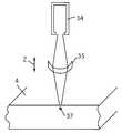
- a faceted lens 64is positioned in the rear portion of the beam exiting the cylinder lens 62 .
- Faceted lens 64is preferably made from the same materials as the other lenses 70 , 72 , 60 , and 62 and is designed to transmit the beam at the wavelength produced by the laser 54 .
- the faceted lens 64has an upper or lower surface that is defined by angled or sloped surfaces 88 meeting in the center a spine 90 .
- the angled surfaces 88are preferably angled ⁇ from the horizontal by approximately 0.75°.
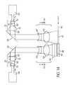
- the movable mirror 140is placed in its preheat position before engaging the motion system to preheat the region to be cut on the substrate 4 .
- the mirror 140is moved to its second position so that the beam path goes through its primary beam path and the separation by the scribe and break beams can commence.
- the scribe and break beamsare moved to contact the substrate 4 as soon as possible after the preheating to minimize the radiant and conductive cooling effects.
Landscapes
- Physics & Mathematics (AREA)
- Optics & Photonics (AREA)
- Engineering & Computer Science (AREA)
- Plasma & Fusion (AREA)
- Mechanical Engineering (AREA)
- Chemical & Material Sciences (AREA)
- Health & Medical Sciences (AREA)
- Toxicology (AREA)
- General Physics & Mathematics (AREA)
- Chemical Kinetics & Catalysis (AREA)
- General Chemical & Material Sciences (AREA)
- Manufacturing & Machinery (AREA)
- Computer Hardware Design (AREA)
- Microelectronics & Electronic Packaging (AREA)
- Power Engineering (AREA)
- Condensed Matter Physics & Semiconductors (AREA)
- Oil, Petroleum & Natural Gas (AREA)
- Thermal Sciences (AREA)
- Materials Engineering (AREA)
- Organic Chemistry (AREA)
- Re-Forming, After-Treatment, Cutting And Transporting Of Glass Products (AREA)
- Laser Beam Processing (AREA)
Abstract
Description
Claims (24)
Priority Applications (1)
| Application Number | Priority Date | Filing Date | Title |
|---|---|---|---|
| US09/240,057US6211488B1 (en) | 1998-12-01 | 1999-01-29 | Method and apparatus for separating non-metallic substrates utilizing a laser initiated scribe |
Applications Claiming Priority (2)
| Application Number | Priority Date | Filing Date | Title |
|---|---|---|---|
| US11053398P | 1998-12-01 | 1998-12-01 | |
| US09/240,057US6211488B1 (en) | 1998-12-01 | 1999-01-29 | Method and apparatus for separating non-metallic substrates utilizing a laser initiated scribe |
Publications (1)
| Publication Number | Publication Date |
|---|---|
| US6211488B1true US6211488B1 (en) | 2001-04-03 |
Family
ID=26808124
Family Applications (1)
| Application Number | Title | Priority Date | Filing Date |
|---|---|---|---|
| US09/240,057Expired - Fee RelatedUS6211488B1 (en) | 1998-12-01 | 1999-01-29 | Method and apparatus for separating non-metallic substrates utilizing a laser initiated scribe |
Country Status (1)
| Country | Link |
|---|---|
| US (1) | US6211488B1 (en) |
Cited By (127)
| Publication number | Priority date | Publication date | Assignee | Title |
|---|---|---|---|---|
| WO2002034682A1 (en)* | 2000-10-24 | 2002-05-02 | Georges Cuvelier | Method and installation for cutting out glass pieces |
| US6407360B1 (en)* | 1998-08-26 | 2002-06-18 | Samsung Electronics, Co., Ltd. | Laser cutting apparatus and method |
| US6407363B2 (en)* | 2000-03-30 | 2002-06-18 | Electro Scientific Industries, Inc. | Laser system and method for single press micromachining of multilayer workpieces |
| US6420678B1 (en)* | 1998-12-01 | 2002-07-16 | Brian L. Hoekstra | Method for separating non-metallic substrates |
| US20020195434A1 (en)* | 2001-06-21 | 2002-12-26 | Samsung Electronics Co., Ltd. | Method and apparatus for cutting a substrate into multiple pieces with a single irradiation of a laser beam |
| US20030006220A1 (en)* | 2001-07-02 | 2003-01-09 | Michael Cummings | Method of ablating an opening in a hard, non-metallic substrate |
| US20030019897A1 (en)* | 2001-07-27 | 2003-01-30 | Hannstar Display Corp. | Method for separating a brittle material |
| US20030180731A1 (en)* | 2002-03-25 | 2003-09-25 | Worrall Joseph A. | Methods for producing glass substrates for use in biopolymeric microarrays |
| US6660963B2 (en)* | 1999-11-24 | 2003-12-09 | Applied Photonics, Inc. | Method and apparatus for separating non-metallic materials |
| US20040002199A1 (en)* | 2000-09-13 | 2004-01-01 | Hamamatsu Photonics K.K. | Laser processing method and laser processing apparatus |
| US6734083B2 (en)* | 2001-08-28 | 2004-05-11 | Tokyo Seimitsu Co., Ltd. | Dicing method and dicing apparatus for dicing plate-like workpiece |
| US6744009B1 (en) | 2002-04-02 | 2004-06-01 | Seagate Technology Llc | Combined laser-scribing and laser-breaking for shaping of brittle substrates |
| KR20040046421A (en)* | 2002-11-27 | 2004-06-05 | 주식회사 이오테크닉스 | Apparatus and method for cutting brittle material using laser |
| US20040141145A1 (en)* | 2000-05-23 | 2004-07-22 | Hitachi, Ltd. | Method for producing a liquid crystal display apparatus |
| US6787732B1 (en) | 2002-04-02 | 2004-09-07 | Seagate Technology Llc | Method for laser-scribing brittle substrates and apparatus therefor |
| US20040188400A1 (en)* | 2001-09-10 | 2004-09-30 | Micron Technology, Inc. | Wafer dicing device and method |
| US6812430B2 (en)* | 2000-12-01 | 2004-11-02 | Lg Electronics Inc. | Glass cutting method and apparatus with controlled laser beam energy |
| US20040221451A1 (en)* | 2003-05-06 | 2004-11-11 | Micron Technology, Inc. | Method for packaging circuits and packaged circuits |
| US20040232124A1 (en)* | 2003-05-19 | 2004-11-25 | Yusuke Nagai | Workpiece dividing method utilizing laser beam |
| US20050009301A1 (en)* | 2003-06-26 | 2005-01-13 | Yusuke Nagai | Semiconductor wafer dividing method utilizing laser beam |
| US20050006361A1 (en)* | 2003-07-11 | 2005-01-13 | Satoshi Kobayashi | Machining apparatus utilizing laser beam |
| US20050029239A1 (en)* | 2001-09-21 | 2005-02-10 | Masato Matsumoto | Method for scribing substrate of brittle material and scriber |
| US20050045090A1 (en)* | 2003-09-01 | 2005-03-03 | Hiroshi Ikegami | Apparatus for laser beam machining, machining mask, method for laser beam machining, method for manufacturing a semiconductor device and semiconductor device |
| US20050067392A1 (en)* | 2003-09-26 | 2005-03-31 | Yusuke Nagai | Dividing method and apparatus for sheet-shaped workpiece |
| US20050069000A1 (en)* | 2003-09-26 | 2005-03-31 | Yusuke Nagai | Dividing method and apparatus for sheet-shaped workpiece |
| US20050098548A1 (en)* | 2003-11-06 | 2005-05-12 | Satoshi Kobayashi | Processing apparatus using laser beam |
| US20050109742A1 (en)* | 2003-10-27 | 2005-05-26 | Yusuke Nagai | Processing method using laser beam |
| US20050130390A1 (en)* | 2003-12-11 | 2005-06-16 | Peter Andrews | Semiconductor substrate assemblies and methods for preparing and dicing the same |
| US20050202596A1 (en)* | 2002-03-12 | 2005-09-15 | Fumitsugu Fukuyo | Laser processing method |
| DE102004014276A1 (en)* | 2004-03-22 | 2005-10-13 | Grenzebach Maschinenbau Gmbh | Longitudinal cutting of moving flat glass strips from float glass plates with warming of the plates by a laser beam followed by breakage of the strips off the plates |
| US20050244600A1 (en)* | 2004-04-28 | 2005-11-03 | Wycech Joseph S | Method and apparatus for forming a finished article of manufacture and a finished article of manufacture made by a new and novel process |
| US20050252943A1 (en)* | 2004-05-11 | 2005-11-17 | Lg Philips Lcd Co., Ltd. | Apparatus and method for scribing substrate |
| US20050263503A1 (en)* | 2002-08-21 | 2005-12-01 | Brzesowsky Rudolf H | Method of breaking a brittle substrate |
| US20050272223A1 (en)* | 2002-03-12 | 2005-12-08 | Yoshimaro Fujii | Method for dicing substrate |
| US20060021978A1 (en)* | 2002-02-21 | 2006-02-02 | Alexeev Andrey M | Method for cutting non-metallic materials and device for carring out said method |
| US20060022008A1 (en)* | 2004-07-30 | 2006-02-02 | Brown James W | Process and apparatus for scoring a brittle material |
| US20060021977A1 (en)* | 2004-07-30 | 2006-02-02 | Menegus Harry E | Process and apparatus for scoring a brittle material incorporating moving optical assembly |
| US20060040472A1 (en)* | 2004-08-17 | 2006-02-23 | Denso Corporation | Method for separating semiconductor substrate |
| US20060076327A1 (en)* | 2004-10-07 | 2006-04-13 | Disco Corporation | Laser beam processing machine |
| US20060076326A1 (en)* | 2004-09-28 | 2006-04-13 | Disco Corporation | Laser beam processing machine |
| US20060086704A1 (en)* | 2004-10-27 | 2006-04-27 | Disco Corporation | Laser beam processing method and laser beam processing machine |
| US20060101858A1 (en)* | 2003-01-10 | 2006-05-18 | Masahiro Fujii | Brittle material substrate scribing device and scribing method, and automatic analysis line |
| US20060113287A1 (en)* | 2004-11-26 | 2006-06-01 | Canon Kabushiki Kaisha | Laser cutting method |
| US20060151450A1 (en)* | 2003-01-06 | 2006-07-13 | Ki-Yong You | Glass-plate cutting machine |
| US20060179722A1 (en)* | 2005-02-02 | 2006-08-17 | Spindler Robert G | Edge treatment for glass panes |
| US20060258047A1 (en)* | 2005-05-11 | 2006-11-16 | Canon Kabushiki Kaisha | Method for laser cutting and method of producing function elements |
| US20060255024A1 (en)* | 2003-03-11 | 2006-11-16 | Fumitsufu Fukuyo | Laser beam machining method |
| WO2007032392A1 (en) | 2005-09-16 | 2007-03-22 | Hamamatsu Photonics K.K. | Laser processing method and laser processing device |
| US20070085099A1 (en)* | 2003-09-10 | 2007-04-19 | Kenshi Fukumitsu | Semiconductor substrate cutting method |
| JP2007152958A (en)* | 2005-12-05 | 2007-06-21 | Foxsemicon Intergated Technology Inc | Laser cutting equipment |
| US20070158314A1 (en)* | 2003-03-12 | 2007-07-12 | Kenshi Fukumitsu | Laser processing method |
| US20070170159A1 (en)* | 2003-07-18 | 2007-07-26 | Hamamatsu Photonics K.K. | Laser beam machining method, laser beam machining apparatus, and laser beam machining product |
| US20070252154A1 (en)* | 2003-09-11 | 2007-11-01 | Shoichi Uchiyama | Semiconductor Chip Manufacturing Method, Semiconductor Chip, Semiconductor Thin Film Chip, Electron Tube and Photo-Detecting Device |
| KR100799434B1 (en) | 2005-09-12 | 2008-01-30 | 폭스세미콘 인티그리티드 테크놀로지, 인코포레이티드 | Laser cutting device and method |
| US20080037003A1 (en)* | 2004-01-09 | 2008-02-14 | Kazuhiro Atsumi | Laser Processing Method And Device |
| US20080053972A1 (en)* | 2002-03-12 | 2008-03-06 | Mitsuboshi Diamond Industrial Co., Ltd. | Method and apparatus for processing brittle material |
| RU2320549C2 (en)* | 2006-04-14 | 2008-03-27 | Учреждение образования "Гомельский государственный университет имени Франциска Скорины" | Method for separating of friable non-metallic materials by subjecting to thermoelastic stress |
| US20080094711A1 (en)* | 2006-10-11 | 2008-04-24 | Oleg Efimov | Methods and apparatus for recording holographic gratings |
| US20080145282A1 (en)* | 2006-10-11 | 2008-06-19 | Oleg Efimov | Methods and apparatus for thermal development of large area solids |
| CN100411825C (en)* | 2001-07-16 | 2008-08-20 | 三星宝石工业株式会社 | Scribing device for brittle material substrate and scribing method for brittle material substrate |
| US20080218735A1 (en)* | 2004-01-09 | 2008-09-11 | Hamamatsu Photonics K.K. | Laser Processing Method And Device |
| US20080251506A1 (en)* | 2004-01-09 | 2008-10-16 | Kazuhiro Atsumi | Laser Processing Method and Device |
| US20080288734A1 (en)* | 2007-05-15 | 2008-11-20 | Pitney Bowes Incorporated | Mail processing computer automatic recovery system and method |
| US20080283509A1 (en)* | 2007-05-15 | 2008-11-20 | Anatoli Anatolyevich Abramov | Method and apparatus for scoring and separating a brittle material with a single beam of radiation |
| US20090014425A1 (en)* | 2007-07-12 | 2009-01-15 | Jenoptik Automatisierungstechnik Gmbh | Method and device for dividing a plane-parallel plate made of a brittle material into a plurality of individual plates by means of a laser |
| US20090061597A1 (en)* | 2007-08-30 | 2009-03-05 | Kavlico Corporation | Singulator method and apparatus |
| US20090085254A1 (en)* | 2007-09-28 | 2009-04-02 | Anatoli Anatolyevich Abramov | Laser scoring with flat profile beam |
| US20090120134A1 (en)* | 2007-11-09 | 2009-05-14 | Xin Chen | Method and apparatus for measuring surface shape profile |
| US20090126403A1 (en)* | 2007-11-20 | 2009-05-21 | Abramov Anatoli A | Laser scoring of glass sheets at high speeds and with low residual stress |
| EA012311B1 (en)* | 2006-08-16 | 2009-08-28 | Общество С Ограниченной Ответственностью "Лазтекс" | Method for cutting brittle transparent non-metal materials by laser |
| US20090224432A1 (en)* | 2004-12-08 | 2009-09-10 | Syohei Nagatomo | Method of forming split originating point on object to be split, method of splitting object to be split, and method of processing object to be processed by pulse laser beam |
| US20090230102A1 (en)* | 2005-10-28 | 2009-09-17 | Masanobu Soyama | Method for Creating Scribe Line on Brittle Material Substrate and Apparatus for Creating Scribe Line |
| US7626138B2 (en) | 2005-09-08 | 2009-12-01 | Imra America, Inc. | Transparent material processing with an ultrashort pulse laser |
| US20090294419A1 (en)* | 2008-05-27 | 2009-12-03 | Corning Incorporated | Scoring of non-flat materials |
| US20100025387A1 (en)* | 2005-09-08 | 2010-02-04 | Imra America, Inc. | Transparent material processing with an ultrashort pulse laser |
| RU2383500C2 (en)* | 2008-05-04 | 2010-03-10 | Учреждение образования "Гомельский государственный университет имени Франциска Скорины" | Method to cut non-metal materials |
| US20100078417A1 (en)* | 2008-09-29 | 2010-04-01 | Anatoli Anatolyevich Abramov | Laser separation of glass sheets |
| US20100102042A1 (en)* | 2008-10-23 | 2010-04-29 | Sean Matthew Garner | Non-contact glass shearing device and method for scribing or cutting a moving glass sheet |
| US20100140794A1 (en)* | 2001-10-08 | 2010-06-10 | Chia Yong Poo | Apparatus and method for packaging circuits |
| US20100149553A1 (en)* | 2008-12-16 | 2010-06-17 | Xin Chen | Method and Apparatus for Determining Sheet Position During Production and Handling |
| US20100197116A1 (en)* | 2008-03-21 | 2010-08-05 | Imra America, Inc. | Laser-based material processing methods and systems |
| US20100206008A1 (en)* | 2009-02-19 | 2010-08-19 | Harvey Daniel R | Method of separating strengthened glass |
| US20100212361A1 (en)* | 2009-02-24 | 2010-08-26 | Anatoli Anatolyevich Abramov | Method for scoring a sheet of brittle material |
| US20100240159A1 (en)* | 2007-09-06 | 2010-09-23 | Hamamatsu Photonics K.K. | Manufacturing method of semiconductor laser element |
| US20100279067A1 (en)* | 2009-04-30 | 2010-11-04 | Robert Sabia | Glass sheet having enhanced edge strength |
| US20100291353A1 (en)* | 2009-02-19 | 2010-11-18 | Matthew John Dejneka | Method of separating strengthened glass |
| US20110018143A1 (en)* | 2002-06-14 | 2011-01-27 | Swee Kwang Chua | Wafer level packaging |
| US20110049765A1 (en)* | 2009-08-28 | 2011-03-03 | Xinghua Li | Methods for Laser Cutting Glass Substrates |
| US20110113830A1 (en)* | 2009-11-18 | 2011-05-19 | Abramov Anatoli A | Method for cutting a brittle material |
| US20110127244A1 (en)* | 2009-11-30 | 2011-06-02 | Xinghua Li | Methods for laser scribing and separating glass substrates |
| US20110300692A1 (en)* | 2008-10-29 | 2011-12-08 | Oerlikon Solar Ag, Trubbach | Method for dividing a semiconductor film formed on a substrate into plural regions by multiple laser beam irradiation |
| US20110316200A1 (en)* | 2010-05-14 | 2011-12-29 | Hamamatsu Photonics K.K. | Method of cutting object to be processed, method of cutting strengthened glass sheet and method of manufacturing strengthened glass member |
| US20120000894A1 (en)* | 2009-03-20 | 2012-01-05 | Carrier Corporation | Precision laser scoring |
| US20120047956A1 (en)* | 2010-08-31 | 2012-03-01 | Xinghua Li | Methods of separating strengthened glass substrates |
| US20120061440A1 (en)* | 2009-06-02 | 2012-03-15 | Grenzebach Maschinenbau Gmbh | Method and aparatus for producing an elastically deformable glass plate |
| DE10327360B4 (en)* | 2003-06-16 | 2012-05-24 | Curamik Electronics Gmbh | Method for producing a ceramic-metal substrate |
| US20120135847A1 (en)* | 2009-07-03 | 2012-05-31 | Asahi Glass Company Limited | Method and apparatus for cutting a brittle-material substrate, and window glass for vehicle obtained by the method |
| US8263479B2 (en) | 2002-12-03 | 2012-09-11 | Hamamatsu Photonics K.K. | Method for cutting semiconductor substrate |
| CN101670487B (en)* | 2008-09-12 | 2013-01-09 | 欧姆龙株式会社 | Method and device for forming line used for cutting |
| US20130192305A1 (en)* | 2011-08-10 | 2013-08-01 | Matthew L. Black | Methods for separating glass substrate sheets by laser-formed grooves |
| US20130256286A1 (en)* | 2009-12-07 | 2013-10-03 | Ipg Microsystems Llc | Laser processing using an astigmatic elongated beam spot and using ultrashort pulses and/or longer wavelengths |
| US20140001679A1 (en)* | 2011-01-13 | 2014-01-02 | Hamamatsu Photonics K.K. | Laser processing method |
| US8685838B2 (en) | 2003-03-12 | 2014-04-01 | Hamamatsu Photonics K.K. | Laser beam machining method |
| EP2180970A4 (en)* | 2007-07-24 | 2014-07-02 | Eo Technics Co Ltd | Laser processing apparatus and method using beam split |
| US8816245B2 (en) | 2010-05-14 | 2014-08-26 | Hamamatsu Photonics K.K. | Method of cutting object to be processed |
| US8887529B2 (en) | 2010-10-29 | 2014-11-18 | Corning Incorporated | Method and apparatus for cutting glass ribbon |
| WO2014190968A1 (en)* | 2013-05-29 | 2014-12-04 | Rogers Germany Gmbh | Metal-ceramic substrate and method for producing a metal-ceramic substrate |
| US8943855B2 (en) | 2009-08-28 | 2015-02-03 | Corning Incorporated | Methods for laser cutting articles from ion exchanged glass substrates |
| US9212081B2 (en) | 2012-11-21 | 2015-12-15 | Corning Incorporated | Methods of cutting a laminate strengthened glass substrate |
| US9321126B2 (en) | 2004-03-31 | 2016-04-26 | Imra America, Inc. | Laser-based material processing apparatus and methods |
| KR20160121430A (en)* | 2015-04-09 | 2016-10-19 | 가부시기가이샤 디스코 | Laser machining apparatus |
| US9610653B2 (en) | 2012-09-21 | 2017-04-04 | Electro Scientific Industries, Inc. | Method and apparatus for separation of workpieces and articles produced thereby |
| US20170106476A1 (en)* | 2014-04-04 | 2017-04-20 | Hamamatsu Photonics K.K. | Laser processing device and laser processing method |
| CN106604898A (en)* | 2015-08-10 | 2017-04-26 | 法国圣戈班玻璃厂 | Method for cutting thin glass layers |
| KR20170053111A (en)* | 2015-11-05 | 2017-05-15 | 가부시기가이샤 디스코 | Wafer processing method |
| TWI587956B (en)* | 2013-11-19 | 2017-06-21 | 柔芬新拿科技公司 | Method of closed form release for brittle materials using burst ultrafast laser pulses |
| US9828278B2 (en) | 2012-02-28 | 2017-11-28 | Electro Scientific Industries, Inc. | Method and apparatus for separation of strengthened glass and articles produced thereby |
| US9828277B2 (en) | 2012-02-28 | 2017-11-28 | Electro Scientific Industries, Inc. | Methods for separation of strengthened glass |
| US9938180B2 (en) | 2012-06-05 | 2018-04-10 | Corning Incorporated | Methods of cutting glass using a laser |
| KR20180120281A (en)* | 2016-03-25 | 2018-11-05 | 어플라이드 머티어리얼스, 인코포레이티드 | Hybrid Wafer Dicing Approach Using Rotating Beam Laser Scribing Process and Plasma Etching Process |
| US20190112215A1 (en)* | 2017-10-13 | 2019-04-18 | Seagate Technology Llc | Separation of glass shapes using engineered induced thermal gradients after process cutting |
| US10357850B2 (en) | 2012-09-24 | 2019-07-23 | Electro Scientific Industries, Inc. | Method and apparatus for machining a workpiece |
| US10828719B2 (en) | 2011-09-21 | 2020-11-10 | Align Technology, Inc. | Laser cutting |
| US11217536B2 (en)* | 2016-03-03 | 2022-01-04 | Applied Materials, Inc. | Hybrid wafer dicing approach using a split beam laser scribing process and plasma etch process |
| US20220241902A1 (en)* | 2021-02-01 | 2022-08-04 | Corning Incorporated | Sacrificial layers to enable laser cutting of textured substrates |
| EP4144472A4 (en)* | 2020-04-28 | 2024-03-27 | Iti Co., Ltd. | Ceramic cutting method and equipment |
| CN119317215A (en)* | 2024-08-22 | 2025-01-14 | 江苏永达电力金具有限公司 | Solar cell production equipment |
Citations (22)
| Publication number | Priority date | Publication date | Assignee | Title |
|---|---|---|---|---|
| US3894208A (en) | 1971-02-12 | 1975-07-08 | Wilfried Hellmuth Bergmann | Method of abrasive machining of material by means of an energy beam |
| US3932726A (en) | 1972-10-12 | 1976-01-13 | Glaverbel-Mecaniver S.A. | Glass cutting |
| US3935419A (en) | 1972-10-12 | 1976-01-27 | Glaverbel-Mecaniver S.A. | Severing of glass or vitrocrystalline bodies |
| GB1433563A (en)* | 1973-05-04 | 1976-04-28 | Commissariat Energie Atomique | Method of and apparatus for cutting glass |
| US4092518A (en)* | 1976-12-07 | 1978-05-30 | Laser Technique S.A. | Method of decorating a transparent plastics material article by means of a laser beam |
| US4451872A (en) | 1980-11-26 | 1984-05-29 | Kernforschungsanlage Julich Gesellschaft Mit Beschrankter Haftung | Process for the most uniform illumination of a surface by a collimated beam of rays and arrangement for laser diagnostic |
| US4467168A (en) | 1981-04-01 | 1984-08-21 | Creative Glassworks International | Method of cutting glass with a laser and an article made therewith |
| US4468534A (en) | 1982-09-30 | 1984-08-28 | Boddicker Franc W | Method and device for cutting glass |
| US4937424A (en) | 1987-07-20 | 1990-06-26 | Mitsubishi Denki Kabushiki Kaisha | Laser machining apparatus |
| US5498851A (en) | 1992-08-27 | 1996-03-12 | Mitsubishi Denki Kabushiki Kaisha | Laser machining apparatus and method |
| JPH08175837A (en) | 1994-12-26 | 1996-07-09 | Asahi Glass Co Ltd | Method for cleaving glass plate and apparatus therefor |
| US5630308A (en) | 1990-07-09 | 1997-05-20 | American National Can Company | Laser scoring of packaging substrates |
| US5637244A (en)* | 1993-05-13 | 1997-06-10 | Podarok International, Inc. | Method and apparatus for creating an image by a pulsed laser beam inside a transparent material |
| US5728993A (en) | 1995-08-05 | 1998-03-17 | The Boc Group Plc | Laser cutting of materials with plural beams |
| JPH10116801A (en) | 1996-10-09 | 1998-05-06 | Rohm Co Ltd | Method for dividing substrate and manufacture of light emitting element using the method |
| US5844707A (en) | 1996-01-31 | 1998-12-01 | Asahi Kogaku Kogyo Kabushiki Kaisha | Scanning optical device |
| US5871134A (en) | 1994-12-27 | 1999-02-16 | Asahi Glass Company Ltd. | Method and apparatus for breaking and cutting a glass ribbon |
| US5935464A (en) | 1997-09-11 | 1999-08-10 | Lsp Technologies, Inc. | Laser shock peening apparatus with a diffractive optic element |
| US5961852A (en) | 1997-09-09 | 1999-10-05 | Optical Coating Laboratory, Inc. | Laser scribe and break process |
| US5968382A (en)* | 1995-07-14 | 1999-10-19 | Hitachi, Ltd. | Laser cleavage cutting method and system |
| US6023039A (en) | 1996-10-30 | 2000-02-08 | Nec Corporation | Method of cleaving a brittle material using a point heat source for providing a thermal stress |
| US6037564A (en) | 1998-03-31 | 2000-03-14 | Matsushita Electric Industrial Co., Ltd. | Method for scanning a beam and an apparatus therefor |
- 1999
- 1999-01-29USUS09/240,057patent/US6211488B1/ennot_activeExpired - Fee Related
Patent Citations (22)
| Publication number | Priority date | Publication date | Assignee | Title |
|---|---|---|---|---|
| US3894208A (en) | 1971-02-12 | 1975-07-08 | Wilfried Hellmuth Bergmann | Method of abrasive machining of material by means of an energy beam |
| US3932726A (en) | 1972-10-12 | 1976-01-13 | Glaverbel-Mecaniver S.A. | Glass cutting |
| US3935419A (en) | 1972-10-12 | 1976-01-27 | Glaverbel-Mecaniver S.A. | Severing of glass or vitrocrystalline bodies |
| GB1433563A (en)* | 1973-05-04 | 1976-04-28 | Commissariat Energie Atomique | Method of and apparatus for cutting glass |
| US4092518A (en)* | 1976-12-07 | 1978-05-30 | Laser Technique S.A. | Method of decorating a transparent plastics material article by means of a laser beam |
| US4451872A (en) | 1980-11-26 | 1984-05-29 | Kernforschungsanlage Julich Gesellschaft Mit Beschrankter Haftung | Process for the most uniform illumination of a surface by a collimated beam of rays and arrangement for laser diagnostic |
| US4467168A (en) | 1981-04-01 | 1984-08-21 | Creative Glassworks International | Method of cutting glass with a laser and an article made therewith |
| US4468534A (en) | 1982-09-30 | 1984-08-28 | Boddicker Franc W | Method and device for cutting glass |
| US4937424A (en) | 1987-07-20 | 1990-06-26 | Mitsubishi Denki Kabushiki Kaisha | Laser machining apparatus |
| US5630308A (en) | 1990-07-09 | 1997-05-20 | American National Can Company | Laser scoring of packaging substrates |
| US5498851A (en) | 1992-08-27 | 1996-03-12 | Mitsubishi Denki Kabushiki Kaisha | Laser machining apparatus and method |
| US5637244A (en)* | 1993-05-13 | 1997-06-10 | Podarok International, Inc. | Method and apparatus for creating an image by a pulsed laser beam inside a transparent material |
| JPH08175837A (en) | 1994-12-26 | 1996-07-09 | Asahi Glass Co Ltd | Method for cleaving glass plate and apparatus therefor |
| US5871134A (en) | 1994-12-27 | 1999-02-16 | Asahi Glass Company Ltd. | Method and apparatus for breaking and cutting a glass ribbon |
| US5968382A (en)* | 1995-07-14 | 1999-10-19 | Hitachi, Ltd. | Laser cleavage cutting method and system |
| US5728993A (en) | 1995-08-05 | 1998-03-17 | The Boc Group Plc | Laser cutting of materials with plural beams |
| US5844707A (en) | 1996-01-31 | 1998-12-01 | Asahi Kogaku Kogyo Kabushiki Kaisha | Scanning optical device |
| JPH10116801A (en) | 1996-10-09 | 1998-05-06 | Rohm Co Ltd | Method for dividing substrate and manufacture of light emitting element using the method |
| US6023039A (en) | 1996-10-30 | 2000-02-08 | Nec Corporation | Method of cleaving a brittle material using a point heat source for providing a thermal stress |
| US5961852A (en) | 1997-09-09 | 1999-10-05 | Optical Coating Laboratory, Inc. | Laser scribe and break process |
| US5935464A (en) | 1997-09-11 | 1999-08-10 | Lsp Technologies, Inc. | Laser shock peening apparatus with a diffractive optic element |
| US6037564A (en) | 1998-03-31 | 2000-03-14 | Matsushita Electric Industrial Co., Ltd. | Method for scanning a beam and an apparatus therefor |
Cited By (314)
| Publication number | Priority date | Publication date | Assignee | Title |
|---|---|---|---|---|
| US20030209528A1 (en)* | 1998-08-26 | 2003-11-13 | Choo Dae-Ho | Laser cutting apparatus and method |
| US6407360B1 (en)* | 1998-08-26 | 2002-06-18 | Samsung Electronics, Co., Ltd. | Laser cutting apparatus and method |
| US6723952B2 (en) | 1998-08-26 | 2004-04-20 | Samsung Electronics Co., Ltd. | Laser cutting apparatus and method |
| US6590181B2 (en)* | 1998-08-26 | 2003-07-08 | Samsung Electronics Co., Ltd. | Laser cutter apparatus using two laser beams of different wavelengths |
| US6420678B1 (en)* | 1998-12-01 | 2002-07-16 | Brian L. Hoekstra | Method for separating non-metallic substrates |
| US6660963B2 (en)* | 1999-11-24 | 2003-12-09 | Applied Photonics, Inc. | Method and apparatus for separating non-metallic materials |
| US6407363B2 (en)* | 2000-03-30 | 2002-06-18 | Electro Scientific Industries, Inc. | Laser system and method for single press micromachining of multilayer workpieces |
| US7142278B2 (en)* | 2000-05-23 | 2006-11-28 | Hitachi, Ltd. | Method for producing a liquid crystal display apparatus |
| US20040141145A1 (en)* | 2000-05-23 | 2004-07-22 | Hitachi, Ltd. | Method for producing a liquid crystal display apparatus |
| US20110021004A1 (en)* | 2000-09-13 | 2011-01-27 | Hamamatsu Photonics K.K. | Method of cutting a substrate, method of cutting a wafer-like object, and method of manufacturing a semiconductor device |
| US20110027971A1 (en)* | 2000-09-13 | 2011-02-03 | Hamamatsu Photonics K.K. | Method of cutting a substrate, method of processing a wafer-like object, and method of manufacturing a semiconductor device |
| US20040002199A1 (en)* | 2000-09-13 | 2004-01-01 | Hamamatsu Photonics K.K. | Laser processing method and laser processing apparatus |
| US8933369B2 (en) | 2000-09-13 | 2015-01-13 | Hamamatsu Photonics K.K. | Method of cutting a substrate and method of manufacturing a semiconductor device |
| US8937264B2 (en) | 2000-09-13 | 2015-01-20 | Hamamatsu Photonics K.K. | Laser processing method and laser processing apparatus |
| US8946592B2 (en) | 2000-09-13 | 2015-02-03 | Hamamatsu Photonics K.K. | Laser processing method and laser processing apparatus |
| US7626137B2 (en) | 2000-09-13 | 2009-12-01 | Hamamatsu Photonics K.K. | Laser cutting by forming a modified region within an object and generating fractures |
| US20100055876A1 (en)* | 2000-09-13 | 2010-03-04 | Hamamatsu Photonics K.K. | Laser processing method and laser processing apparatus |
| US8946589B2 (en) | 2000-09-13 | 2015-02-03 | Hamamatsu Photonics K.K. | Method of cutting a substrate, method of cutting a wafer-like object, and method of manufacturing a semiconductor device |
| US20060160331A1 (en)* | 2000-09-13 | 2006-07-20 | Hamamatsu Photonics K.K. | Laser processing method and laser processing apparatus |
| CN101670493A (en)* | 2000-09-13 | 2010-03-17 | 浜松光子学株式会社 | Laser processing method and laser processing apparatus |
| US8946591B2 (en) | 2000-09-13 | 2015-02-03 | Hamamatsu Photonics K.K. | Method of manufacturing a semiconductor device formed using a substrate cutting method |
| US7732730B2 (en)* | 2000-09-13 | 2010-06-08 | Hamamatsu Photonics K.K. | Laser processing method and laser processing apparatus |
| US8969761B2 (en) | 2000-09-13 | 2015-03-03 | Hamamatsu Photonics K.K. | Method of cutting a wafer-like object and semiconductor chip |
| US7547613B2 (en) | 2000-09-13 | 2009-06-16 | Hamamatsu Photonics K.K. | Laser processing method and laser processing apparatus |
| US10796959B2 (en) | 2000-09-13 | 2020-10-06 | Hamamatsu Photonics K.K. | Laser processing method and laser processing apparatus |
| US20060040473A1 (en)* | 2000-09-13 | 2006-02-23 | Hamamatsu Photonics K.K. | Laser processing method and laser processing apparatus |
| CN111633349A (en)* | 2000-09-13 | 2020-09-08 | 浜松光子学株式会社 | Laser processing method and laser processing apparatus |
| US20100176100A1 (en)* | 2000-09-13 | 2010-07-15 | Hamamatsu Photonics K.K. | Laser processing method and laser processing apparatus |
| US7615721B2 (en) | 2000-09-13 | 2009-11-10 | Hamamatsu Photonics K.K. | Laser processing method and laser processing apparatus |
| US7825350B2 (en)* | 2000-09-13 | 2010-11-02 | Hamamatsu Photonics K.K. | Laser processing method and laser processing apparatus |
| CN105108348A (en)* | 2000-09-13 | 2015-12-02 | 浜松光子学株式会社 | Laser processing method and laser processing apparatus |
| US9837315B2 (en) | 2000-09-13 | 2017-12-05 | Hamamatsu Photonics K.K. | Laser processing method and laser processing apparatus |
| US8927900B2 (en) | 2000-09-13 | 2015-01-06 | Hamamatsu Photonics K.K. | Method of cutting a substrate, method of processing a wafer-like object, and method of manufacturing a semiconductor device |
| CN106825940A (en)* | 2000-09-13 | 2017-06-13 | 浜松光子学株式会社 | Laser processing and laser processing device |
| CN103551738B (en)* | 2000-09-13 | 2017-05-17 | 浜松光子学株式会社 | Laser beam machining method and laser beam machining device |
| US20110027972A1 (en)* | 2000-09-13 | 2011-02-03 | Hamamatsu Photonics K.K. | Method of cutting a substrate and method of manufacturing a semiconductor device |
| US7592238B2 (en) | 2000-09-13 | 2009-09-22 | Hamamatsu Photonics K.K. | Laser processing method and laser processing apparatus |
| US20110037149A1 (en)* | 2000-09-13 | 2011-02-17 | Hamamatsu Photonics K.K. | Method of cutting a wafer-like object and semiconductor chip |
| US8716110B2 (en) | 2000-09-13 | 2014-05-06 | Hamamatsu Photonics K.K. | Laser processing method and laser processing apparatus |
| US20050173387A1 (en)* | 2000-09-13 | 2005-08-11 | Hamamatsu Photonics K.K. | Laser processing method and laser processing apparatus |
| US20050181581A1 (en)* | 2000-09-13 | 2005-08-18 | Hamamatsu Photonics K.K. | Laser processing method and laser processing apparatus |
| US20050184037A1 (en)* | 2000-09-13 | 2005-08-25 | Hamamatsu Photonics K.K. | Laser processing method and laser processing apparatus |
| US20050189330A1 (en)* | 2000-09-13 | 2005-09-01 | Hamamatsu Photonics K.K. | Laser processing method and laser processing apparatus |
| US20050194364A1 (en)* | 2000-09-13 | 2005-09-08 | Hamamatsu Photonics K.K. | Laser processing method and laser processing apparatus |
| US7396742B2 (en) | 2000-09-13 | 2008-07-08 | Hamamatsu Photonics K.K. | Laser processing method for cutting a wafer-like object by using a laser to form modified regions within the object |
| US8227724B2 (en) | 2000-09-13 | 2012-07-24 | Hamamatsu Photonics K.K. | Laser processing method and laser processing apparatus |
| US8283595B2 (en) | 2000-09-13 | 2012-10-09 | Hamamatsu Photonics K.K. | Laser processing method and laser processing apparatus |
| US6992026B2 (en) | 2000-09-13 | 2006-01-31 | Hamamatsu Photonics K.K. | Laser processing method and laser processing apparatus |
| CN103551738A (en)* | 2000-09-13 | 2014-02-05 | 浜松光子学株式会社 | Laser beam machining method and laser beam machining device |
| WO2002034682A1 (en)* | 2000-10-24 | 2002-05-02 | Georges Cuvelier | Method and installation for cutting out glass pieces |
| US7002101B2 (en) | 2000-10-24 | 2006-02-21 | Georges Cuvelier | Method and installation for laser cutting out glass pieces |
| US20040016729A1 (en)* | 2000-10-24 | 2004-01-29 | Georges Cuvelier | Method and installation for cutting out glass pieces |
| US6812430B2 (en)* | 2000-12-01 | 2004-11-02 | Lg Electronics Inc. | Glass cutting method and apparatus with controlled laser beam energy |
| US20020195434A1 (en)* | 2001-06-21 | 2002-12-26 | Samsung Electronics Co., Ltd. | Method and apparatus for cutting a substrate into multiple pieces with a single irradiation of a laser beam |
| KR100700997B1 (en)* | 2001-06-21 | 2007-03-28 | 삼성전자주식회사 | Substrate multi cutting method and substrate multi cutting device for performing the same |
| US20040262273A1 (en)* | 2001-06-21 | 2004-12-30 | Hyung-Woo Nam | Method and apparatus for cutting a substrate into multiple pieces with a single irradiation of a laser beam |
| US6770842B2 (en)* | 2001-06-21 | 2004-08-03 | Samsung Electronics Co., Ltd. | Method and apparatus for cutting a substrate into multiple pieces with a single irradiation of a laser beam |
| US20030006220A1 (en)* | 2001-07-02 | 2003-01-09 | Michael Cummings | Method of ablating an opening in a hard, non-metallic substrate |
| CN1308113C (en)* | 2001-07-02 | 2007-04-04 | 维蒂克激光系统公司 | Method of ablating an opening in a hard, non-metallic substrate |
| US6864460B2 (en)* | 2001-07-02 | 2005-03-08 | Virtek Laser Systems, Inc. | Method of ablating an opening in a hard, non-metallic substrate |
| CN100411825C (en)* | 2001-07-16 | 2008-08-20 | 三星宝石工业株式会社 | Scribing device for brittle material substrate and scribing method for brittle material substrate |
| US20030019897A1 (en)* | 2001-07-27 | 2003-01-30 | Hannstar Display Corp. | Method for separating a brittle material |
| US6734083B2 (en)* | 2001-08-28 | 2004-05-11 | Tokyo Seimitsu Co., Ltd. | Dicing method and dicing apparatus for dicing plate-like workpiece |
| US20040188400A1 (en)* | 2001-09-10 | 2004-09-30 | Micron Technology, Inc. | Wafer dicing device and method |
| US20050029239A1 (en)* | 2001-09-21 | 2005-02-10 | Masato Matsumoto | Method for scribing substrate of brittle material and scriber |
| CN1871104B (en)* | 2001-09-21 | 2010-06-23 | 三星钻石工业股份有限公司 | Method for scribing substrate of brittle material and scriber |
| US7772522B2 (en)* | 2001-09-21 | 2010-08-10 | Mitsuboshi Diamond Industrial Co., Ltd. | Method for scribing substrate of brittle material and scriber |
| US20100140794A1 (en)* | 2001-10-08 | 2010-06-10 | Chia Yong Poo | Apparatus and method for packaging circuits |
| US8115306B2 (en) | 2001-10-08 | 2012-02-14 | Round Rock Research, Llc | Apparatus and method for packaging circuits |
| US20060021978A1 (en)* | 2002-02-21 | 2006-02-02 | Alexeev Andrey M | Method for cutting non-metallic materials and device for carring out said method |
| US9543256B2 (en) | 2002-03-12 | 2017-01-10 | Hamamatsu Photonics K.K. | Substrate dividing method |
| US9543207B2 (en) | 2002-03-12 | 2017-01-10 | Hamamatsu Photonics K.K. | Substrate dividing method |
| US8673745B2 (en) | 2002-03-12 | 2014-03-18 | Hamamatsu Photonics K.K. | Method of cutting object to be processed |
| US20050272223A1 (en)* | 2002-03-12 | 2005-12-08 | Yoshimaro Fujii | Method for dicing substrate |
| US7566635B2 (en) | 2002-03-12 | 2009-07-28 | Hamamatsu Photonics K.K. | Substrate dividing method |
| US9287177B2 (en) | 2002-03-12 | 2016-03-15 | Hamamatsu Photonics K.K. | Substrate dividing method |
| US8598015B2 (en) | 2002-03-12 | 2013-12-03 | Hamamatsu Photonics K.K. | Laser processing method |
| US8889525B2 (en) | 2002-03-12 | 2014-11-18 | Hamamatsu Photonics K.K. | Substrate dividing method |
| US8551865B2 (en) | 2002-03-12 | 2013-10-08 | Hamamatsu Photonics K.K. | Method of cutting an object to be processed |
| US8519511B2 (en) | 2002-03-12 | 2013-08-27 | Hamamatsu Photonics K.K. | Substrate dividing method |
| US8518800B2 (en) | 2002-03-12 | 2013-08-27 | Hamamatsu Photonics K.K. | Substrate dividing method |
| US8518801B2 (en) | 2002-03-12 | 2013-08-27 | Hamamatsu Photonics K.K. | Substrate dividing method |
| US8361883B2 (en) | 2002-03-12 | 2013-01-29 | Hamamatsu Photonics K.K. | Laser processing method |
| US8314013B2 (en) | 2002-03-12 | 2012-11-20 | Hamamatsu Photonics K.K. | Semiconductor chip manufacturing method |
| US8304325B2 (en) | 2002-03-12 | 2012-11-06 | Hamamatsu-Photonics K.K. | Substrate dividing method |
| US7749867B2 (en) | 2002-03-12 | 2010-07-06 | Hamamatsu Photonics K.K. | Method of cutting processed object |
| US20080053972A1 (en)* | 2002-03-12 | 2008-03-06 | Mitsuboshi Diamond Industrial Co., Ltd. | Method and apparatus for processing brittle material |
| US8268704B2 (en) | 2002-03-12 | 2012-09-18 | Hamamatsu Photonics K.K. | Method for dicing substrate |
| US20080090382A1 (en)* | 2002-03-12 | 2008-04-17 | Hamamatsu Photonics K.K. | Substrate dividing method |
| US20060121697A1 (en)* | 2002-03-12 | 2006-06-08 | Hamamatsu Photonics K.K. | Substrate dividing method |
| US8183131B2 (en) | 2002-03-12 | 2012-05-22 | Hamamatsu Photonics K. K. | Method of cutting an object to be processed |
| US8802543B2 (en) | 2002-03-12 | 2014-08-12 | Hamamatsu Photonics K.K. | Laser processing method |
| US20060011593A1 (en)* | 2002-03-12 | 2006-01-19 | Fumitsugu Fukuyo | Method of cutting processed object |
| US20050202596A1 (en)* | 2002-03-12 | 2005-09-15 | Fumitsugu Fukuyo | Laser processing method |
| US11424162B2 (en) | 2002-03-12 | 2022-08-23 | Hamamatsu Photonics K.K. | Substrate dividing method |
| US10622255B2 (en) | 2002-03-12 | 2020-04-14 | Hamamatsu Photonics K.K. | Substrate dividing method |
| US9548246B2 (en) | 2002-03-12 | 2017-01-17 | Hamamatsu Photonics K.K. | Substrate dividing method |
| US9553023B2 (en) | 2002-03-12 | 2017-01-24 | Hamamatsu Photonics K.K. | Substrate dividing method |
| US9711405B2 (en) | 2002-03-12 | 2017-07-18 | Hamamatsu Photonics K.K. | Substrate dividing method |
| US9142458B2 (en) | 2002-03-12 | 2015-09-22 | Hamamatsu Photonics K.K. | Substrate dividing method |
| US20100203707A1 (en)* | 2002-03-12 | 2010-08-12 | Hamamatsu Photonics K.K. | Substrate dividing method |
| US10068801B2 (en) | 2002-03-12 | 2018-09-04 | Hamamatsu Photonics K.K. | Substrate dividing method |
| US7816623B2 (en)* | 2002-03-12 | 2010-10-19 | Mitsuboshi Diamond Industrial Co., Ltd. | Method and apparatus for processing brittle material |
| EP1348671A3 (en)* | 2002-03-25 | 2004-10-20 | Agilent Technologies, Inc. | Method for producing glass substrates for use in biopolymeric microarrays |
| US20030180731A1 (en)* | 2002-03-25 | 2003-09-25 | Worrall Joseph A. | Methods for producing glass substrates for use in biopolymeric microarrays |
| US20050150881A1 (en)* | 2002-03-25 | 2005-07-14 | Worrall Joseph A.Iii | Methods for producing glass substrates for use in biopolymeric microarrays |
| US6919531B2 (en)* | 2002-03-25 | 2005-07-19 | Agilent Technologies, Inc. | Methods for producing glass substrates for use in biopolymeric microarrays |
| US7026573B2 (en)* | 2002-03-25 | 2006-04-11 | Agilent Technologies, Inc. | Methods for producing glass substrates for use in biopolymeric microarrays |
| US6787732B1 (en) | 2002-04-02 | 2004-09-07 | Seagate Technology Llc | Method for laser-scribing brittle substrates and apparatus therefor |
| US6744009B1 (en) | 2002-04-02 | 2004-06-01 | Seagate Technology Llc | Combined laser-scribing and laser-breaking for shaping of brittle substrates |
| US8106488B2 (en) | 2002-06-14 | 2012-01-31 | Micron Technology, Inc. | Wafer level packaging |
| US8564106B2 (en) | 2002-06-14 | 2013-10-22 | Micron Technology, Inc. | Wafer level packaging |
| US20110018143A1 (en)* | 2002-06-14 | 2011-01-27 | Swee Kwang Chua | Wafer level packaging |
| US7838795B2 (en)* | 2002-08-21 | 2010-11-23 | Mitsuboshi Diamond Industrial Co., Ltd. | Method of breaking a brittle substrate |
| US20050263503A1 (en)* | 2002-08-21 | 2005-12-01 | Brzesowsky Rudolf H | Method of breaking a brittle substrate |
| KR20040046421A (en)* | 2002-11-27 | 2004-06-05 | 주식회사 이오테크닉스 | Apparatus and method for cutting brittle material using laser |
| US8865566B2 (en) | 2002-12-03 | 2014-10-21 | Hamamatsu Photonics K.K. | Method of cutting semiconductor substrate |
| US8263479B2 (en) | 2002-12-03 | 2012-09-11 | Hamamatsu Photonics K.K. | Method for cutting semiconductor substrate |
| US8409968B2 (en) | 2002-12-03 | 2013-04-02 | Hamamatsu Photonics K.K. | Method of cutting semiconductor substrate via modified region formation and subsequent sheet expansion |
| US8450187B2 (en) | 2002-12-03 | 2013-05-28 | Hamamatsu Photonics K.K. | Method of cutting semiconductor substrate |
| US7642483B2 (en) | 2003-01-06 | 2010-01-05 | Rorze Systems Corporation | Glass-plate cutting machine |
| US20060151450A1 (en)* | 2003-01-06 | 2006-07-13 | Ki-Yong You | Glass-plate cutting machine |
| US7723641B2 (en)* | 2003-01-10 | 2010-05-25 | Mitsuboshi Diamond Industrial Co., Ltd. | Brittle material substrate scribing device and scribing method, and automatic analysis line |
| US20060101858A1 (en)* | 2003-01-10 | 2006-05-18 | Masahiro Fujii | Brittle material substrate scribing device and scribing method, and automatic analysis line |
| US8247734B2 (en) | 2003-03-11 | 2012-08-21 | Hamamatsu Photonics K.K. | Laser beam machining method |
| US20060255024A1 (en)* | 2003-03-11 | 2006-11-16 | Fumitsufu Fukuyo | Laser beam machining method |
| US20070158314A1 (en)* | 2003-03-12 | 2007-07-12 | Kenshi Fukumitsu | Laser processing method |
| US8685838B2 (en) | 2003-03-12 | 2014-04-01 | Hamamatsu Photonics K.K. | Laser beam machining method |
| US8969752B2 (en) | 2003-03-12 | 2015-03-03 | Hamamatsu Photonics K.K. | Laser processing method |
| US8555495B2 (en) | 2003-05-06 | 2013-10-15 | Micron Technology, Inc. | Method for packaging circuits |
| US20100146780A1 (en)* | 2003-05-06 | 2010-06-17 | Yong Poo Chia | Method for packaging circuits and packaged circuits |
| US7712211B2 (en) | 2003-05-06 | 2010-05-11 | Micron Technology, Inc. | Method for packaging circuits and packaged circuits |
| US8065792B2 (en) | 2003-05-06 | 2011-11-29 | Micron Technology, Inc. | Method for packaging circuits |
| US10453704B2 (en) | 2003-05-06 | 2019-10-22 | Micron Technology, Inc. | Method for packaging circuits |
| US20040221451A1 (en)* | 2003-05-06 | 2004-11-11 | Micron Technology, Inc. | Method for packaging circuits and packaged circuits |
| US9484225B2 (en) | 2003-05-06 | 2016-11-01 | Micron Technology, Inc. | Method for packaging circuits |
| US10811278B2 (en) | 2003-05-06 | 2020-10-20 | Micron Technology, Inc. | Method for packaging circuits |
| US20040232124A1 (en)* | 2003-05-19 | 2004-11-25 | Yusuke Nagai | Workpiece dividing method utilizing laser beam |
| US20080128953A1 (en)* | 2003-05-19 | 2008-06-05 | Yusuke Nagai | Workpiece dividing method utilizing laser beam |
| DE102004024643B4 (en)* | 2003-05-19 | 2011-07-28 | Disco Corp. | Workpiece division method using a laser beam |
| DE10327360B4 (en)* | 2003-06-16 | 2012-05-24 | Curamik Electronics Gmbh | Method for producing a ceramic-metal substrate |
| US20050009301A1 (en)* | 2003-06-26 | 2005-01-13 | Yusuke Nagai | Semiconductor wafer dividing method utilizing laser beam |
| CN100365761C (en)* | 2003-06-26 | 2008-01-30 | 株式会社迪斯科 | Semiconductor Wafer Separation Method Using Laser |
| US7141443B2 (en) | 2003-06-26 | 2006-11-28 | Disco Corporation | Semiconductor wafer dividing method utilizing laser beam |
| US20050006361A1 (en)* | 2003-07-11 | 2005-01-13 | Satoshi Kobayashi | Machining apparatus utilizing laser beam |
| US20100151202A1 (en)* | 2003-07-18 | 2010-06-17 | Hamamatsu Photonics K.K. | Laser beam machining method, laser beam machining apparatus, and laser beam machining product |
| US8852698B2 (en) | 2003-07-18 | 2014-10-07 | Hamamatsu Photonics K.K. | Laser beam machining method, laser beam machining apparatus, and laser beam machining product |
| US20070170159A1 (en)* | 2003-07-18 | 2007-07-26 | Hamamatsu Photonics K.K. | Laser beam machining method, laser beam machining apparatus, and laser beam machining product |
| US7605344B2 (en) | 2003-07-18 | 2009-10-20 | Hamamatsu Photonics K.K. | Laser beam machining method, laser beam machining apparatus, and laser beam machining product |
| US20050045090A1 (en)* | 2003-09-01 | 2005-03-03 | Hiroshi Ikegami | Apparatus for laser beam machining, machining mask, method for laser beam machining, method for manufacturing a semiconductor device and semiconductor device |
| US20100203678A1 (en)* | 2003-09-10 | 2010-08-12 | Hamamatsu Photonics K.K. | Semiconductor substrate cutting method |
| US20070085099A1 (en)* | 2003-09-10 | 2007-04-19 | Kenshi Fukumitsu | Semiconductor substrate cutting method |
| US8551817B2 (en) | 2003-09-10 | 2013-10-08 | Hamamatsu Photonics K.K. | Semiconductor substrate cutting method |
| US8058103B2 (en) | 2003-09-10 | 2011-11-15 | Hamamatsu Photonics K.K. | Semiconductor substrate cutting method |
| US20070252154A1 (en)* | 2003-09-11 | 2007-11-01 | Shoichi Uchiyama | Semiconductor Chip Manufacturing Method, Semiconductor Chip, Semiconductor Thin Film Chip, Electron Tube and Photo-Detecting Device |
| US20050067392A1 (en)* | 2003-09-26 | 2005-03-31 | Yusuke Nagai | Dividing method and apparatus for sheet-shaped workpiece |
| US20050069000A1 (en)* | 2003-09-26 | 2005-03-31 | Yusuke Nagai | Dividing method and apparatus for sheet-shaped workpiece |
| CN100436030C (en)* | 2003-10-27 | 2008-11-26 | 株式会社迪斯科 | Processing method using laser beam |
| US20050109742A1 (en)* | 2003-10-27 | 2005-05-26 | Yusuke Nagai | Processing method using laser beam |
| DE102004053329B4 (en)* | 2003-11-06 | 2014-02-13 | Disco Corp. | Processing device using a laser beam |
| US7405376B2 (en) | 2003-11-06 | 2008-07-29 | Disco Corporation | Processing apparatus using laser beam |
| US20050098548A1 (en)* | 2003-11-06 | 2005-05-12 | Satoshi Kobayashi | Processing apparatus using laser beam |
| US7008861B2 (en)* | 2003-12-11 | 2006-03-07 | Cree, Inc. | Semiconductor substrate assemblies and methods for preparing and dicing the same |
| WO2005062376A1 (en)* | 2003-12-11 | 2005-07-07 | Cree, Inc. | Semiconductor substrate assemblies and methods for preparing and dicing the same |
| US20050130390A1 (en)* | 2003-12-11 | 2005-06-16 | Peter Andrews | Semiconductor substrate assemblies and methods for preparing and dicing the same |
| US9511449B2 (en) | 2004-01-09 | 2016-12-06 | Hamamatsu Photonics K.K. | Laser processing method and device |
| US10293433B2 (en) | 2004-01-09 | 2019-05-21 | Hamamatsu Photonics K.K. | Laser processing method and device |
| US8993922B2 (en) | 2004-01-09 | 2015-03-31 | Hamamatsu Photonics K.K. | Laser processing method and device |
| US9352414B2 (en) | 2004-01-09 | 2016-05-31 | Hamamatsu Photonics K.K. | Laser processing method and device |
| US20080218735A1 (en)* | 2004-01-09 | 2008-09-11 | Hamamatsu Photonics K.K. | Laser Processing Method And Device |
| US11241757B2 (en) | 2004-01-09 | 2022-02-08 | Hamamatsu Photonics K.K. | Laser processing method and device |
| US8624153B2 (en) | 2004-01-09 | 2014-01-07 | Hamamatsu Photonics K.K. | Laser processing method and device |
| US20080251506A1 (en)* | 2004-01-09 | 2008-10-16 | Kazuhiro Atsumi | Laser Processing Method and Device |
| US20080037003A1 (en)* | 2004-01-09 | 2008-02-14 | Kazuhiro Atsumi | Laser Processing Method And Device |
| DE102004014276A1 (en)* | 2004-03-22 | 2005-10-13 | Grenzebach Maschinenbau Gmbh | Longitudinal cutting of moving flat glass strips from float glass plates with warming of the plates by a laser beam followed by breakage of the strips off the plates |
| US9321126B2 (en) | 2004-03-31 | 2016-04-26 | Imra America, Inc. | Laser-based material processing apparatus and methods |
| US20050244600A1 (en)* | 2004-04-28 | 2005-11-03 | Wycech Joseph S | Method and apparatus for forming a finished article of manufacture and a finished article of manufacture made by a new and novel process |
| US20050252943A1 (en)* | 2004-05-11 | 2005-11-17 | Lg Philips Lcd Co., Ltd. | Apparatus and method for scribing substrate |
| US7934976B2 (en)* | 2004-05-11 | 2011-05-03 | Lg Display Co., Ltd. | Apparatus and method for scribing substrate |
| US7820941B2 (en) | 2004-07-30 | 2010-10-26 | Corning Incorporated | Process and apparatus for scoring a brittle material |
| US20060021977A1 (en)* | 2004-07-30 | 2006-02-02 | Menegus Harry E | Process and apparatus for scoring a brittle material incorporating moving optical assembly |
| US20060022008A1 (en)* | 2004-07-30 | 2006-02-02 | Brown James W | Process and apparatus for scoring a brittle material |
| US7550367B2 (en)* | 2004-08-17 | 2009-06-23 | Denso Corporation | Method for separating semiconductor substrate |
| US20060040472A1 (en)* | 2004-08-17 | 2006-02-23 | Denso Corporation | Method for separating semiconductor substrate |
| US20060076326A1 (en)* | 2004-09-28 | 2006-04-13 | Disco Corporation | Laser beam processing machine |
| US7482553B2 (en)* | 2004-09-28 | 2009-01-27 | Disco Corporation | Laser beam processing machine |
| US20060076327A1 (en)* | 2004-10-07 | 2006-04-13 | Disco Corporation | Laser beam processing machine |
| US20070243696A1 (en)* | 2004-10-07 | 2007-10-18 | Satoshi Kobayashi | Laser beam processing machine |
| US7538048B2 (en) | 2004-10-07 | 2009-05-26 | Disco Corporation | Laser beam processing machine |
| US7223937B2 (en) | 2004-10-27 | 2007-05-29 | Disco Corporation | Laser beam processing method and laser beam processing machine |
| US20060086704A1 (en)* | 2004-10-27 | 2006-04-27 | Disco Corporation | Laser beam processing method and laser beam processing machine |
| US8108998B2 (en)* | 2004-11-26 | 2012-02-07 | Canon Kabushiki Kaisha | Laser cutting method |
| US20060113287A1 (en)* | 2004-11-26 | 2006-06-01 | Canon Kabushiki Kaisha | Laser cutting method |
| US20090224432A1 (en)* | 2004-12-08 | 2009-09-10 | Syohei Nagatomo | Method of forming split originating point on object to be split, method of splitting object to be split, and method of processing object to be processed by pulse laser beam |
| US20060179722A1 (en)* | 2005-02-02 | 2006-08-17 | Spindler Robert G | Edge treatment for glass panes |
| US20060258047A1 (en)* | 2005-05-11 | 2006-11-16 | Canon Kabushiki Kaisha | Method for laser cutting and method of producing function elements |
| US8389891B2 (en) | 2005-09-08 | 2013-03-05 | Imra America, Inc. | Transparent material processing with an ultrashort pulse laser |
| US20100025387A1 (en)* | 2005-09-08 | 2010-02-04 | Imra America, Inc. | Transparent material processing with an ultrashort pulse laser |
| US8530786B2 (en) | 2005-09-08 | 2013-09-10 | Imra America, Inc. | Transparent material processing with an ultrashort pulse laser |
| US8314359B2 (en) | 2005-09-08 | 2012-11-20 | Imra America, Inc. | Methods and systems for laser welding transparent materials with an ultrashort pulsed laser |
| US20100086741A1 (en)* | 2005-09-08 | 2010-04-08 | Imra America, Inc. | Transparent material processing with an ultrashort pulse laser |
| US9751154B2 (en) | 2005-09-08 | 2017-09-05 | Imra America, Inc. | Transparent material processing with an ultrashort pulse laser |
| US20100084384A1 (en)* | 2005-09-08 | 2010-04-08 | Imra America, Inc. | Transparent material processing with an ultrashort pulse laser |
| US9636773B2 (en) | 2005-09-08 | 2017-05-02 | Imra America, Inc. | Transparent material processing with an ultrashort pulse laser |
| US7626138B2 (en) | 2005-09-08 | 2009-12-01 | Imra America, Inc. | Transparent material processing with an ultrashort pulse laser |
| US9138913B2 (en) | 2005-09-08 | 2015-09-22 | Imra America, Inc. | Transparent material processing with an ultrashort pulse laser |
| KR100799434B1 (en) | 2005-09-12 | 2008-01-30 | 폭스세미콘 인티그리티드 테크놀로지, 인코포레이티드 | Laser cutting device and method |
| TWI463550B (en)* | 2005-09-16 | 2014-12-01 | Hamamatsu Photonics Kk | Laser processing method and laser processing device |
| US20090261083A1 (en)* | 2005-09-16 | 2009-10-22 | Hamamatsu Photonics K.K. | Laser processing method and laser processing device |
| US8513567B2 (en) | 2005-09-16 | 2013-08-20 | Hamamatsu Photonics K.K. | Laser processing method for forming a modified region for cutting in an object |
| WO2007032392A1 (en) | 2005-09-16 | 2007-03-22 | Hamamatsu Photonics K.K. | Laser processing method and laser processing device |
| EP1944118A4 (en)* | 2005-09-16 | 2009-09-16 | Hamamatsu Photonics Kk | Laser processing method and laser processing device |
| US20090230102A1 (en)* | 2005-10-28 | 2009-09-17 | Masanobu Soyama | Method for Creating Scribe Line on Brittle Material Substrate and Apparatus for Creating Scribe Line |
| JP2007152958A (en)* | 2005-12-05 | 2007-06-21 | Foxsemicon Intergated Technology Inc | Laser cutting equipment |
| RU2320549C2 (en)* | 2006-04-14 | 2008-03-27 | Учреждение образования "Гомельский государственный университет имени Франциска Скорины" | Method for separating of friable non-metallic materials by subjecting to thermoelastic stress |
| EA012311B1 (en)* | 2006-08-16 | 2009-08-28 | Общество С Ограниченной Ответственностью "Лазтекс" | Method for cutting brittle transparent non-metal materials by laser |
| US8043087B2 (en) | 2006-10-11 | 2011-10-25 | Raytheon Company | Methods and apparatus for thermal development of large area solids |
| US20080145282A1 (en)* | 2006-10-11 | 2008-06-19 | Oleg Efimov | Methods and apparatus for thermal development of large area solids |
| US20080094711A1 (en)* | 2006-10-11 | 2008-04-24 | Oleg Efimov | Methods and apparatus for recording holographic gratings |
| US7982162B2 (en)* | 2007-05-15 | 2011-07-19 | Corning Incorporated | Method and apparatus for scoring and separating a brittle material with a single beam of radiation |
| WO2008140818A3 (en)* | 2007-05-15 | 2009-05-22 | Corning Inc | Method and apparatus for scoring and separating a brittle material with a single beam of radiation |
| US20080283509A1 (en)* | 2007-05-15 | 2008-11-20 | Anatoli Anatolyevich Abramov | Method and apparatus for scoring and separating a brittle material with a single beam of radiation |
| US20080288734A1 (en)* | 2007-05-15 | 2008-11-20 | Pitney Bowes Incorporated | Mail processing computer automatic recovery system and method |
| US20090014425A1 (en)* | 2007-07-12 | 2009-01-15 | Jenoptik Automatisierungstechnik Gmbh | Method and device for dividing a plane-parallel plate made of a brittle material into a plurality of individual plates by means of a laser |
| US8110777B2 (en)* | 2007-07-12 | 2012-02-07 | Jenoptik Automatisierungstechnik Gmbh | Method and device for dividing a plane-parallel plate made of a brittle material into a plurality of individual plates by means of a laser |
| EP2180970A4 (en)* | 2007-07-24 | 2014-07-02 | Eo Technics Co Ltd | Laser processing apparatus and method using beam split |
| US20090061597A1 (en)* | 2007-08-30 | 2009-03-05 | Kavlico Corporation | Singulator method and apparatus |
| CN101796698B (en)* | 2007-09-06 | 2012-06-27 | 浜松光子学株式会社 | Manufacturing method of semiconductor laser element |
| KR101522746B1 (en)* | 2007-09-06 | 2015-05-26 | 하마마츠 포토닉스 가부시키가이샤 | Manufacturing method of semiconductor laser element |
| US20100240159A1 (en)* | 2007-09-06 | 2010-09-23 | Hamamatsu Photonics K.K. | Manufacturing method of semiconductor laser element |
| US8110422B2 (en)* | 2007-09-06 | 2012-02-07 | Hamamatsu Photonics K.K. | Manufacturing method of semiconductor laser element |
| US20090085254A1 (en)* | 2007-09-28 | 2009-04-02 | Anatoli Anatolyevich Abramov | Laser scoring with flat profile beam |
| US8402785B2 (en) | 2007-11-09 | 2013-03-26 | Corning Incorporated | Method and apparatus for measuring surface shape profile |
| US20090120134A1 (en)* | 2007-11-09 | 2009-05-14 | Xin Chen | Method and apparatus for measuring surface shape profile |
| US8011207B2 (en) | 2007-11-20 | 2011-09-06 | Corning Incorporated | Laser scoring of glass sheets at high speeds and with low residual stress |
| US20090126403A1 (en)* | 2007-11-20 | 2009-05-21 | Abramov Anatoli A | Laser scoring of glass sheets at high speeds and with low residual stress |
| US8158493B2 (en) | 2008-03-21 | 2012-04-17 | Imra America, Inc. | Laser-based material processing methods and systems |
| US20100197116A1 (en)* | 2008-03-21 | 2010-08-05 | Imra America, Inc. | Laser-based material processing methods and systems |
| US8785813B2 (en) | 2008-03-21 | 2014-07-22 | Imra America, Inc. | Laser-based material processing methods and systems |
| RU2383500C2 (en)* | 2008-05-04 | 2010-03-10 | Учреждение образования "Гомельский государственный университет имени Франциска Скорины" | Method to cut non-metal materials |
| US20090294419A1 (en)* | 2008-05-27 | 2009-12-03 | Corning Incorporated | Scoring of non-flat materials |
| US8053704B2 (en) | 2008-05-27 | 2011-11-08 | Corning Incorporated | Scoring of non-flat materials |
| CN101670487B (en)* | 2008-09-12 | 2013-01-09 | 欧姆龙株式会社 | Method and device for forming line used for cutting |
| US20100078417A1 (en)* | 2008-09-29 | 2010-04-01 | Anatoli Anatolyevich Abramov | Laser separation of glass sheets |
| US8051679B2 (en) | 2008-09-29 | 2011-11-08 | Corning Incorporated | Laser separation of glass sheets |
| KR20110091685A (en)* | 2008-10-23 | 2011-08-12 | 코닝 인코포레이티드 | Non-contact glass shear apparatus and method for drawing a line or cutting the glass sheet to move |
| US8895892B2 (en) | 2008-10-23 | 2014-11-25 | Corning Incorporated | Non-contact glass shearing device and method for scribing or cutting a moving glass sheet |
| US20100102042A1 (en)* | 2008-10-23 | 2010-04-29 | Sean Matthew Garner | Non-contact glass shearing device and method for scribing or cutting a moving glass sheet |
| US20110300692A1 (en)* | 2008-10-29 | 2011-12-08 | Oerlikon Solar Ag, Trubbach | Method for dividing a semiconductor film formed on a substrate into plural regions by multiple laser beam irradiation |
| US8058634B2 (en) | 2008-12-16 | 2011-11-15 | Corning Incorporated | Method and apparatus for determining sheet position using information from two distinct light beams each at a different position and a different angle |
| US20100149553A1 (en)* | 2008-12-16 | 2010-06-17 | Xin Chen | Method and Apparatus for Determining Sheet Position During Production and Handling |
| US20100291353A1 (en)* | 2009-02-19 | 2010-11-18 | Matthew John Dejneka | Method of separating strengthened glass |
| US8341976B2 (en) | 2009-02-19 | 2013-01-01 | Corning Incorporated | Method of separating strengthened glass |
| WO2010096359A1 (en)* | 2009-02-19 | 2010-08-26 | Corning Incorporated | Method of separating strengthened glass |
| US8327666B2 (en) | 2009-02-19 | 2012-12-11 | Corning Incorporated | Method of separating strengthened glass |
| US20100206008A1 (en)* | 2009-02-19 | 2010-08-19 | Harvey Daniel R | Method of separating strengthened glass |
| US20100212361A1 (en)* | 2009-02-24 | 2010-08-26 | Anatoli Anatolyevich Abramov | Method for scoring a sheet of brittle material |
| US8245540B2 (en)* | 2009-02-24 | 2012-08-21 | Corning Incorporated | Method for scoring a sheet of brittle material |
| US20120000894A1 (en)* | 2009-03-20 | 2012-01-05 | Carrier Corporation | Precision laser scoring |
| US9302346B2 (en)* | 2009-03-20 | 2016-04-05 | Corning, Incorporated | Precision laser scoring |
| US20100279067A1 (en)* | 2009-04-30 | 2010-11-04 | Robert Sabia | Glass sheet having enhanced edge strength |
| US20120061440A1 (en)* | 2009-06-02 | 2012-03-15 | Grenzebach Maschinenbau Gmbh | Method and aparatus for producing an elastically deformable glass plate |
| US8939337B2 (en)* | 2009-06-02 | 2015-01-27 | Grenzebach Maschinenbau Gmbh | Method and apparatus for producing an elastically deformable glass plate |
| US20120135847A1 (en)* | 2009-07-03 | 2012-05-31 | Asahi Glass Company Limited | Method and apparatus for cutting a brittle-material substrate, and window glass for vehicle obtained by the method |
| USRE49530E1 (en) | 2009-08-21 | 2023-05-16 | Corning Incorporated | Crack and scratch resistant glass and enclosures made therefrom |
| US20110049765A1 (en)* | 2009-08-28 | 2011-03-03 | Xinghua Li | Methods for Laser Cutting Glass Substrates |
| KR20120064091A (en)* | 2009-08-28 | 2012-06-18 | 코닝 인코포레이티드 | Methods for laser cutting glass substrates |
| TWI490179B (en)* | 2009-08-28 | 2015-07-01 | Corning Inc | Method for laser cutting glass substrate |
| US8932510B2 (en)* | 2009-08-28 | 2015-01-13 | Corning Incorporated | Methods for laser cutting glass substrates |
| US9533910B2 (en) | 2009-08-28 | 2017-01-03 | Corning Incorporated | Methods for laser cutting glass substrates |
| US8943855B2 (en) | 2009-08-28 | 2015-02-03 | Corning Incorporated | Methods for laser cutting articles from ion exchanged glass substrates |
| US20110113830A1 (en)* | 2009-11-18 | 2011-05-19 | Abramov Anatoli A | Method for cutting a brittle material |
| US8171753B2 (en) | 2009-11-18 | 2012-05-08 | Corning Incorporated | Method for cutting a brittle material |
| US20110127244A1 (en)* | 2009-11-30 | 2011-06-02 | Xinghua Li | Methods for laser scribing and separating glass substrates |
| US8946590B2 (en) | 2009-11-30 | 2015-02-03 | Corning Incorporated | Methods for laser scribing and separating glass substrates |
| US10358374B2 (en) | 2009-11-30 | 2019-07-23 | Corning Incorporated | Methods for laser scribing and separating glass substrates |
| US20130256286A1 (en)* | 2009-12-07 | 2013-10-03 | Ipg Microsystems Llc | Laser processing using an astigmatic elongated beam spot and using ultrashort pulses and/or longer wavelengths |
| US8950217B2 (en)* | 2010-05-14 | 2015-02-10 | Hamamatsu Photonics K.K. | Method of cutting object to be processed, method of cutting strengthened glass sheet and method of manufacturing strengthened glass member |
| US8816245B2 (en) | 2010-05-14 | 2014-08-26 | Hamamatsu Photonics K.K. | Method of cutting object to be processed |
| US20110316200A1 (en)* | 2010-05-14 | 2011-12-29 | Hamamatsu Photonics K.K. | Method of cutting object to be processed, method of cutting strengthened glass sheet and method of manufacturing strengthened glass member |
| US8720228B2 (en)* | 2010-08-31 | 2014-05-13 | Corning Incorporated | Methods of separating strengthened glass substrates |
| US20120047956A1 (en)* | 2010-08-31 | 2012-03-01 | Xinghua Li | Methods of separating strengthened glass substrates |
| US8887529B2 (en) | 2010-10-29 | 2014-11-18 | Corning Incorporated | Method and apparatus for cutting glass ribbon |
| US9295969B2 (en)* | 2011-01-13 | 2016-03-29 | Hamamatsu Photonics K.K. | Laser processing method |
| US20140001679A1 (en)* | 2011-01-13 | 2014-01-02 | Hamamatsu Photonics K.K. | Laser processing method |
| US10532431B2 (en) | 2011-01-13 | 2020-01-14 | Hamamatsu Photonics K.K. | Laser processing method |
| US20130192305A1 (en)* | 2011-08-10 | 2013-08-01 | Matthew L. Black | Methods for separating glass substrate sheets by laser-formed grooves |
| US8635887B2 (en)* | 2011-08-10 | 2014-01-28 | Corning Incorporated | Methods for separating glass substrate sheets by laser-formed grooves |
| US10828719B2 (en) | 2011-09-21 | 2020-11-10 | Align Technology, Inc. | Laser cutting |
| US11383322B2 (en)* | 2011-09-21 | 2022-07-12 | Align Technology, Inc. | Laser cutting |
| US11534861B2 (en)* | 2011-09-21 | 2022-12-27 | Align Technology, Inc. | Laser cutting |
| US20240066628A1 (en)* | 2011-09-21 | 2024-02-29 | Align Technology, Inc. | Laser cutting |
| US12377493B2 (en)* | 2011-09-21 | 2025-08-05 | Align Technology, Inc. | Laser cutting |
| US9828277B2 (en) | 2012-02-28 | 2017-11-28 | Electro Scientific Industries, Inc. | Methods for separation of strengthened glass |
| US9828278B2 (en) | 2012-02-28 | 2017-11-28 | Electro Scientific Industries, Inc. | Method and apparatus for separation of strengthened glass and articles produced thereby |
| US9938180B2 (en) | 2012-06-05 | 2018-04-10 | Corning Incorporated | Methods of cutting glass using a laser |
| US9610653B2 (en) | 2012-09-21 | 2017-04-04 | Electro Scientific Industries, Inc. | Method and apparatus for separation of workpieces and articles produced thereby |
| US10357850B2 (en) | 2012-09-24 | 2019-07-23 | Electro Scientific Industries, Inc. | Method and apparatus for machining a workpiece |
| US9212081B2 (en) | 2012-11-21 | 2015-12-15 | Corning Incorporated | Methods of cutting a laminate strengthened glass substrate |
| WO2014190968A1 (en)* | 2013-05-29 | 2014-12-04 | Rogers Germany Gmbh | Metal-ceramic substrate and method for producing a metal-ceramic substrate |
| TWI587956B (en)* | 2013-11-19 | 2017-06-21 | 柔芬新拿科技公司 | Method of closed form release for brittle materials using burst ultrafast laser pulses |
| US11007607B2 (en)* | 2014-04-04 | 2021-05-18 | Hamamatsu Photonics K.K. | Laser processing device and laser processing method |
| US20170106476A1 (en)* | 2014-04-04 | 2017-04-20 | Hamamatsu Photonics K.K. | Laser processing device and laser processing method |
| KR20160121430A (en)* | 2015-04-09 | 2016-10-19 | 가부시기가이샤 디스코 | Laser machining apparatus |
| CN106604898A (en)* | 2015-08-10 | 2017-04-26 | 法国圣戈班玻璃厂 | Method for cutting thin glass layers |
| KR20170053111A (en)* | 2015-11-05 | 2017-05-15 | 가부시기가이샤 디스코 | Wafer processing method |
| US11217536B2 (en)* | 2016-03-03 | 2022-01-04 | Applied Materials, Inc. | Hybrid wafer dicing approach using a split beam laser scribing process and plasma etch process |
| KR20180120281A (en)* | 2016-03-25 | 2018-11-05 | 어플라이드 머티어리얼스, 인코포레이티드 | Hybrid Wafer Dicing Approach Using Rotating Beam Laser Scribing Process and Plasma Etching Process |
| US20190112215A1 (en)* | 2017-10-13 | 2019-04-18 | Seagate Technology Llc | Separation of glass shapes using engineered induced thermal gradients after process cutting |
| US10689286B2 (en)* | 2017-10-13 | 2020-06-23 | Seagate Technology Llc | Separation of glass shapes using engineered induced thermal gradients after process cutting |
| EP4144472A4 (en)* | 2020-04-28 | 2024-03-27 | Iti Co., Ltd. | Ceramic cutting method and equipment |
| US20220241902A1 (en)* | 2021-02-01 | 2022-08-04 | Corning Incorporated | Sacrificial layers to enable laser cutting of textured substrates |
| US12304005B2 (en)* | 2021-02-01 | 2025-05-20 | Corning Incorporated | Sacrificial layers to enable laser cutting of textured substrates |
| CN119317215A (en)* | 2024-08-22 | 2025-01-14 | 江苏永达电力金具有限公司 | Solar cell production equipment |
Similar Documents
| Publication | Publication Date | Title |
|---|---|---|
| US6211488B1 (en) | Method and apparatus for separating non-metallic substrates utilizing a laser initiated scribe | |
| US6420678B1 (en) | Method for separating non-metallic substrates | |
| US6259058B1 (en) | Apparatus for separating non-metallic substrates | |
| US6252197B1 (en) | Method and apparatus for separating non-metallic substrates utilizing a supplemental mechanical force applicator | |
| US11053156B2 (en) | Method of closed form release for brittle materials using burst ultrafast laser pulses | |
| US6800831B1 (en) | Method and device for rapid cutting of a workpiece from a brittle material | |
| CN105209218B (en) | The method and apparatus that the processing based on laser is carried out to flat substrate | |
| JP5113462B2 (en) | Method for chamfering a brittle material substrate | |
| EP2898982B1 (en) | Method for laser processing of silicon by filamentation of burst ultrafast laser pulses | |
| JP5525491B2 (en) | Control of crack depth in laser scoring. | |
| US20180360175A1 (en) | Method and apparatus for machining diamonds and gemstones using filamentation by burst ultrafast laser pulses | |
| US6660963B2 (en) | Method and apparatus for separating non-metallic materials | |
| US6787732B1 (en) | Method for laser-scribing brittle substrates and apparatus therefor | |
| US6541730B2 (en) | Method and apparatus for cutting a non-metal substrate by using a laser beam | |
| TWI375602B (en) | ||
| US20020006765A1 (en) | System for cutting brittle materials | |
| US20070284785A1 (en) | Device, System and Method for Cutting, Cleaving or Separating a Substrate Material | |
| US20080283509A1 (en) | Method and apparatus for scoring and separating a brittle material with a single beam of radiation | |
| TW201536460A (en) | Laser cutting of display glass compositions | |
| KR101163394B1 (en) | Method for the freeform cutting of curved substrates made from brittle material | |
| CN102123817B (en) | Decorner processing device | |
| JPWO2009078324A1 (en) | Method and apparatus for chamfering a brittle material substrate | |
| US7002101B2 (en) | Method and installation for laser cutting out glass pieces | |
| JP2005212364A (en) | Brittle material cleaving system and method | |
| JPWO2004002705A1 (en) | Scribing apparatus and scribing method for brittle material substrate |
Legal Events
| Date | Code | Title | Description |
|---|---|---|---|
| AS | Assignment | Owner name:ACCUDYNE DISPLAY AND SEMICONDUCTOR SYSTEMS, INC., Free format text:ASSIGNMENT OF ASSIGNORS INTEREST;ASSIGNORS:GLEBOV, LEONID B.;EFIMOV, OLEG M.;REEL/FRAME:010105/0623 Effective date:19990609 Owner name:ACCUDYNE DISPLAY AND SEMICONDUCTOR SYSTEMS, INC., Free format text:ASSIGNMENT OF ASSIGNORS INTEREST;ASSIGNOR:HOEKSTRA, BRIAN L.;REEL/FRAME:010105/0558 Effective date:19990714 | |
| AS | Assignment | Owner name:LASERDYNE LABS, INC., FLORIDA Free format text:ASSIGNMENT OF ASSIGNORS INTEREST;ASSIGNOR:ACCUDYNE DISPLAY AND SEMICONDUCTOR;REEL/FRAME:012621/0242 Effective date:20020117 | |
| REMI | Maintenance fee reminder mailed | ||
| LAPS | Lapse for failure to pay maintenance fees | ||
| STCH | Information on status: patent discontinuation | Free format text:PATENT EXPIRED DUE TO NONPAYMENT OF MAINTENANCE FEES UNDER 37 CFR 1.362 | |
| FP | Lapsed due to failure to pay maintenance fee | Effective date:20050403 | |
| AS | Assignment | Owner name:INLIGN CPI, LLC, ARIZONA Free format text:SECURITY AGREEMENT;ASSIGNOR:APPLIED PHOTONICS, INC.;REEL/FRAME:016674/0509 Effective date:20050708 | |
| AS | Assignment | Owner name:INLIGN CP I, LLC, ARIZONA Free format text:AMENDMENT TO SECURITY AGREEMENT;ASSIGNOR:APPLIED PHOTONICS, INC.;REEL/FRAME:016712/0501 Effective date:20050901 | |
| AS | Assignment | Owner name:INLIGN CP I, LLC, ARIZONA Free format text:RELEASE OF SECURITY INTERESTS IN PATENTS;ASSIGNOR:APPLIED PHOTONICS, INC.;REEL/FRAME:016967/0432 Effective date:20051031 | |
| AS | Assignment | Owner name:APPLIED PHOTONICS, INC., ARIZONA Free format text:CORRECTIVE DOCUMENT TO CORRECT THE ASSIGNOR AND ASSIGNEE, PREVIOUSLY RECORDED ON REEL 016967 FRAME 0432. ASSIGNOR HEREBY CONFIRMS THE RELEASE OF SECURITY INTERESTS IN PATENTS.;ASSIGNOR:INLIGN CP I, LLC;REEL/FRAME:017336/0131 Effective date:20051031 |