US6211485B1 - Blind via laser drilling system - Google Patents
Blind via laser drilling systemDownload PDFInfo
- Publication number
- US6211485B1 US6211485B1US09/194,933US19493398AUS6211485B1US 6211485 B1US6211485 B1US 6211485B1US 19493398 AUS19493398 AUS 19493398AUS 6211485 B1US6211485 B1US 6211485B1
- Authority
- US
- United States
- Prior art keywords
- laser
- blind
- panel
- laser drilling
- drilling
- Prior art date
- Legal status (The legal status is an assumption and is not a legal conclusion. Google has not performed a legal analysis and makes no representation as to the accuracy of the status listed.)
- Expired - Lifetime
Links
Images


Classifications
- H—ELECTRICITY
- H05—ELECTRIC TECHNIQUES NOT OTHERWISE PROVIDED FOR
- H05K—PRINTED CIRCUITS; CASINGS OR CONSTRUCTIONAL DETAILS OF ELECTRIC APPARATUS; MANUFACTURE OF ASSEMBLAGES OF ELECTRICAL COMPONENTS
- H05K3/00—Apparatus or processes for manufacturing printed circuits
- H05K3/46—Manufacturing multilayer circuits
- H05K3/4644—Manufacturing multilayer circuits by building the multilayer layer by layer, i.e. build-up multilayer circuits
- H05K3/4679—Aligning added circuit layers or via connections relative to previous circuit layers
- B—PERFORMING OPERATIONS; TRANSPORTING
- B23—MACHINE TOOLS; METAL-WORKING NOT OTHERWISE PROVIDED FOR
- B23K—SOLDERING OR UNSOLDERING; WELDING; CLADDING OR PLATING BY SOLDERING OR WELDING; CUTTING BY APPLYING HEAT LOCALLY, e.g. FLAME CUTTING; WORKING BY LASER BEAM
- B23K26/00—Working by laser beam, e.g. welding, cutting or boring
- B23K26/02—Positioning or observing the workpiece, e.g. with respect to the point of impact; Aligning, aiming or focusing the laser beam
- B23K26/06—Shaping the laser beam, e.g. by masks or multi-focusing
- B23K26/064—Shaping the laser beam, e.g. by masks or multi-focusing by means of optical elements, e.g. lenses, mirrors or prisms
- B23K26/066—Shaping the laser beam, e.g. by masks or multi-focusing by means of optical elements, e.g. lenses, mirrors or prisms by using masks
- B—PERFORMING OPERATIONS; TRANSPORTING
- B23—MACHINE TOOLS; METAL-WORKING NOT OTHERWISE PROVIDED FOR
- B23K—SOLDERING OR UNSOLDERING; WELDING; CLADDING OR PLATING BY SOLDERING OR WELDING; CUTTING BY APPLYING HEAT LOCALLY, e.g. FLAME CUTTING; WORKING BY LASER BEAM
- B23K26/00—Working by laser beam, e.g. welding, cutting or boring
- B23K26/08—Devices involving relative movement between laser beam and workpiece
- B23K26/083—Devices involving movement of the workpiece in at least one axial direction
- B23K26/0853—Devices involving movement of the workpiece in at least in two axial directions, e.g. in a plane
- B—PERFORMING OPERATIONS; TRANSPORTING
- B23—MACHINE TOOLS; METAL-WORKING NOT OTHERWISE PROVIDED FOR
- B23K—SOLDERING OR UNSOLDERING; WELDING; CLADDING OR PLATING BY SOLDERING OR WELDING; CUTTING BY APPLYING HEAT LOCALLY, e.g. FLAME CUTTING; WORKING BY LASER BEAM
- B23K26/00—Working by laser beam, e.g. welding, cutting or boring
- B23K26/20—Bonding
- B23K26/21—Bonding by welding
- B23K26/24—Seam welding
- B23K26/28—Seam welding of curved planar seams
- B23K26/282—Seam welding of curved planar seams of tube sections
- B—PERFORMING OPERATIONS; TRANSPORTING
- B23—MACHINE TOOLS; METAL-WORKING NOT OTHERWISE PROVIDED FOR
- B23K—SOLDERING OR UNSOLDERING; WELDING; CLADDING OR PLATING BY SOLDERING OR WELDING; CUTTING BY APPLYING HEAT LOCALLY, e.g. FLAME CUTTING; WORKING BY LASER BEAM
- B23K26/00—Working by laser beam, e.g. welding, cutting or boring
- B23K26/36—Removing material
- B23K26/38—Removing material by boring or cutting
- B23K26/382—Removing material by boring or cutting by boring
- B23K26/389—Removing material by boring or cutting by boring of fluid openings, e.g. nozzles, jets
- H—ELECTRICITY
- H05—ELECTRIC TECHNIQUES NOT OTHERWISE PROVIDED FOR
- H05K—PRINTED CIRCUITS; CASINGS OR CONSTRUCTIONAL DETAILS OF ELECTRIC APPARATUS; MANUFACTURE OF ASSEMBLAGES OF ELECTRICAL COMPONENTS
- H05K3/00—Apparatus or processes for manufacturing printed circuits
- H05K3/0011—Working of insulating substrates or insulating layers
- H05K3/0017—Etching of the substrate by chemical or physical means
- H05K3/0026—Etching of the substrate by chemical or physical means by laser ablation
- H05K3/0032—Etching of the substrate by chemical or physical means by laser ablation of organic insulating material
- H05K3/0035—Etching of the substrate by chemical or physical means by laser ablation of organic insulating material of blind holes, i.e. having a metal layer at the bottom
- H—ELECTRICITY
- H05—ELECTRIC TECHNIQUES NOT OTHERWISE PROVIDED FOR
- H05K—PRINTED CIRCUITS; CASINGS OR CONSTRUCTIONAL DETAILS OF ELECTRIC APPARATUS; MANUFACTURE OF ASSEMBLAGES OF ELECTRICAL COMPONENTS
- H05K1/00—Printed circuits
- H05K1/02—Details
- H05K1/0266—Marks, test patterns or identification means
- H05K1/0269—Marks, test patterns or identification means for visual or optical inspection
- H—ELECTRICITY
- H05—ELECTRIC TECHNIQUES NOT OTHERWISE PROVIDED FOR
- H05K—PRINTED CIRCUITS; CASINGS OR CONSTRUCTIONAL DETAILS OF ELECTRIC APPARATUS; MANUFACTURE OF ASSEMBLAGES OF ELECTRICAL COMPONENTS
- H05K1/00—Printed circuits
- H05K1/02—Details
- H05K1/11—Printed elements for providing electric connections to or between printed circuits
- H05K1/111—Pads for surface mounting, e.g. lay-out
- H05K1/112—Pads for surface mounting, e.g. lay-out directly combined with via connections
- H—ELECTRICITY
- H05—ELECTRIC TECHNIQUES NOT OTHERWISE PROVIDED FOR
- H05K—PRINTED CIRCUITS; CASINGS OR CONSTRUCTIONAL DETAILS OF ELECTRIC APPARATUS; MANUFACTURE OF ASSEMBLAGES OF ELECTRICAL COMPONENTS
- H05K1/00—Printed circuits
- H05K1/16—Printed circuits incorporating printed electric components, e.g. printed resistor, capacitor, inductor
- H05K1/167—Printed circuits incorporating printed electric components, e.g. printed resistor, capacitor, inductor incorporating printed resistors
- H—ELECTRICITY
- H05—ELECTRIC TECHNIQUES NOT OTHERWISE PROVIDED FOR
- H05K—PRINTED CIRCUITS; CASINGS OR CONSTRUCTIONAL DETAILS OF ELECTRIC APPARATUS; MANUFACTURE OF ASSEMBLAGES OF ELECTRICAL COMPONENTS
- H05K2201/00—Indexing scheme relating to printed circuits covered by H05K1/00
- H05K2201/09—Shape and layout
- H05K2201/09209—Shape and layout details of conductors
- H05K2201/095—Conductive through-holes or vias
- H05K2201/09509—Blind vias, i.e. vias having one side closed
- H05K2201/09518—Deep blind vias, i.e. blind vias connecting the surface circuit to circuit layers deeper than the first buried circuit layer
- H—ELECTRICITY
- H05—ELECTRIC TECHNIQUES NOT OTHERWISE PROVIDED FOR
- H05K—PRINTED CIRCUITS; CASINGS OR CONSTRUCTIONAL DETAILS OF ELECTRIC APPARATUS; MANUFACTURE OF ASSEMBLAGES OF ELECTRICAL COMPONENTS
- H05K2201/00—Indexing scheme relating to printed circuits covered by H05K1/00
- H05K2201/09—Shape and layout
- H05K2201/09818—Shape or layout details not covered by a single group of H05K2201/09009 - H05K2201/09809
- H05K2201/09918—Optically detected marks used for aligning tool relative to the PCB, e.g. for mounting of components
- H—ELECTRICITY
- H05—ELECTRIC TECHNIQUES NOT OTHERWISE PROVIDED FOR
- H05K—PRINTED CIRCUITS; CASINGS OR CONSTRUCTIONAL DETAILS OF ELECTRIC APPARATUS; MANUFACTURE OF ASSEMBLAGES OF ELECTRICAL COMPONENTS
- H05K2203/00—Indexing scheme relating to apparatus or processes for manufacturing printed circuits covered by H05K3/00
- H05K2203/01—Tools for processing; Objects used during processing
- H05K2203/0147—Carriers and holders
- H05K2203/0165—Holder for holding a Printed Circuit Board [PCB] during processing, e.g. during screen printing
- H—ELECTRICITY
- H05—ELECTRIC TECHNIQUES NOT OTHERWISE PROVIDED FOR
- H05K—PRINTED CIRCUITS; CASINGS OR CONSTRUCTIONAL DETAILS OF ELECTRIC APPARATUS; MANUFACTURE OF ASSEMBLAGES OF ELECTRICAL COMPONENTS
- H05K2203/00—Indexing scheme relating to apparatus or processes for manufacturing printed circuits covered by H05K3/00
- H05K2203/05—Patterning and lithography; Masks; Details of resist
- H05K2203/0548—Masks
- H05K2203/0554—Metal used as mask for etching vias, e.g. by laser ablation
- H—ELECTRICITY
- H05—ELECTRIC TECHNIQUES NOT OTHERWISE PROVIDED FOR
- H05K—PRINTED CIRCUITS; CASINGS OR CONSTRUCTIONAL DETAILS OF ELECTRIC APPARATUS; MANUFACTURE OF ASSEMBLAGES OF ELECTRICAL COMPONENTS
- H05K2203/00—Indexing scheme relating to apparatus or processes for manufacturing printed circuits covered by H05K3/00
- H05K2203/05—Patterning and lithography; Masks; Details of resist
- H05K2203/0548—Masks
- H05K2203/056—Using an artwork, i.e. a photomask for exposing photosensitive layers
- H—ELECTRICITY
- H05—ELECTRIC TECHNIQUES NOT OTHERWISE PROVIDED FOR
- H05K—PRINTED CIRCUITS; CASINGS OR CONSTRUCTIONAL DETAILS OF ELECTRIC APPARATUS; MANUFACTURE OF ASSEMBLAGES OF ELECTRICAL COMPONENTS
- H05K2203/00—Indexing scheme relating to apparatus or processes for manufacturing printed circuits covered by H05K3/00
- H05K2203/08—Treatments involving gases
- H05K2203/081—Blowing of gas, e.g. for cooling or for providing heat during solder reflowing
- H—ELECTRICITY
- H05—ELECTRIC TECHNIQUES NOT OTHERWISE PROVIDED FOR
- H05K—PRINTED CIRCUITS; CASINGS OR CONSTRUCTIONAL DETAILS OF ELECTRIC APPARATUS; MANUFACTURE OF ASSEMBLAGES OF ELECTRICAL COMPONENTS
- H05K2203/00—Indexing scheme relating to apparatus or processes for manufacturing printed circuits covered by H05K3/00
- H05K2203/08—Treatments involving gases
- H05K2203/082—Suction, e.g. for holding solder balls or components
- H—ELECTRICITY
- H05—ELECTRIC TECHNIQUES NOT OTHERWISE PROVIDED FOR
- H05K—PRINTED CIRCUITS; CASINGS OR CONSTRUCTIONAL DETAILS OF ELECTRIC APPARATUS; MANUFACTURE OF ASSEMBLAGES OF ELECTRICAL COMPONENTS
- H05K3/00—Apparatus or processes for manufacturing printed circuits
- H05K3/0008—Apparatus or processes for manufacturing printed circuits for aligning or positioning of tools relative to the circuit board
- H—ELECTRICITY
- H05—ELECTRIC TECHNIQUES NOT OTHERWISE PROVIDED FOR
- H05K—PRINTED CIRCUITS; CASINGS OR CONSTRUCTIONAL DETAILS OF ELECTRIC APPARATUS; MANUFACTURE OF ASSEMBLAGES OF ELECTRICAL COMPONENTS
- H05K3/00—Apparatus or processes for manufacturing printed circuits
- H05K3/46—Manufacturing multilayer circuits
- H05K3/4611—Manufacturing multilayer circuits by laminating two or more circuit boards
- H05K3/4638—Aligning and fixing the circuit boards before lamination; Detecting or measuring the misalignment after lamination; Aligning external circuit patterns or via connections relative to internal circuits
- H—ELECTRICITY
- H05—ELECTRIC TECHNIQUES NOT OTHERWISE PROVIDED FOR
- H05K—PRINTED CIRCUITS; CASINGS OR CONSTRUCTIONAL DETAILS OF ELECTRIC APPARATUS; MANUFACTURE OF ASSEMBLAGES OF ELECTRICAL COMPONENTS
- H05K3/00—Apparatus or processes for manufacturing printed circuits
- H05K3/46—Manufacturing multilayer circuits
- H05K3/4644—Manufacturing multilayer circuits by building the multilayer layer by layer, i.e. build-up multilayer circuits
- H05K3/4652—Adding a circuit layer by laminating a metal foil or a preformed metal foil pattern
Definitions
- the present inventionrelates to a laser system and method of forming economical and reliable blind vias in circuit boards and polymer based multichip modules.
- Laser drilled blind viasare constructed by positioning and pulsing laser beam radiation over a pre-etched window to remove dielectric material.
- pre-etched windowsas a mask for laser drilling multilayer circuit boards is disclosed in U.S. Pat. No. 4,642,160.
- Fine pitch quad flat packs(FIG. 15) with 0.305 mm centers and ball grid arrays (BGA) (FIG. 13) lead the packaging challenge as the component footprints are designed with finer I/O pitches as shown by microBGA's in FIG. 14 .
- the preferred solution for interconnecting these dense component footprints on the circuit boarddemands blind via technology.
- blind via technologyhas been available for many years but the complex processes needed to produce these blind vias have typically doubled the cost of a circuit board or polymer based multichip module.
- Four different blind via technologiesare known and practiced, but all of these interconnect improvements increase the overall costs of the circuit board and have not openly received broad industry acceptance.
- Plasma etchinguses copper as a mask and photovia typically does not. Both plasma etching of blind vias and photovia process are limited to interconnecting one layer down due to the chemical mechanism used for removing dielectric and are called batch processes. Multiple depth processing is accomplished through sequential layer processing, with multiple layer interconnections achieved by Z-Axis daisy chains. This process for making multiple depth blind via interconnections is called sequential buildup technology. Plasma etching demands a dielectric polymer that can readily be chemical etched. This creates some limitations in material selection, similar to the laser processing described in this disclosure, but to a greater extent. Close process control is necessary in order to not overetch the via crater and create a barreled via that is considerably more difficult to metallize.
- Photovia blind via processingrequires a dielectric polymer that has been chemically processed to be photo-sensitive to generally visible light, a ultraviolet light or near ultraviolet light. These photo-sensitive polymers tend to be quite expensive and generally do not meet the requirements for higher performance circuits. Most photovia processing requires additive or semi-additive plating which yields less surface adhesion. This reduced surface adhesion is considered dangerous for most surface mounted components, especially where ball grid array, flip chip and chip scale packaging technology is the chosen component interconnect scheme.
- the fourth blind via technologyis laser based.
- Several different laser technologiesincluding Eximer, Nd:YAG (neodymium-doped, yttrium-aluminum-garnet) and CO2 (Carbon Dioxide) have successfully drilled blind vias in circuit boards.
- the main limitationhas been the quantity of panels that can be processed by a single laser system. This is best understood by calculating the blind vias drilled per minute or per second on a given panel. Each panel may have one or many replicated circuit designs that will yield finished circuit boards.
- Both the Eximer and the Nd:YAGhave extremely small beam sizes—smaller than the diameter of small blind vias. Eximer lasers are quite expensive to run and require ongoing maintenance.
- Nd:YAG laserMaking blind vias of 0.102 mm to 0.203 mm diameter require a complicated trepanning procedure with the Nd:YAG laser.
- the beamis moved in a spiraling fashion until it removes or ablates the dielectric material from the entire diameter of the via.
- Another limiting factor with a Nd:YAG beamis that the beam energy is readily absorbed by the copper clad material and, therefore, has to be processed at an extremely low energy level and consequently pulsed multiple times while trepanning.
- the Nd:YAG laserrequires recharging after 60 hours of use.
- the sealed RF excited CO2 laser system described in this disclosurehas a 20,000 hour life before recharging according to the supplier Synrad, Inc.
- Another type of CO2 laser systemuses a Transverse Excited Atmospheric (TEA) mechanism to control the pulsing of the CO2 laser.
- TEA CO2 laser system produced by Lumonicsthat is designed for laser drilling blind vias is limited to 150 pulses per second plus with the low 40 watt laser, it is only capable of vaporizing 0.0254 mm of dielectric material with a single pulse. In other words, 0.127 mm of dielectric material would take 5 pulses and the pulse limitation would be at 30 pulses per second.
- the most common alignment for thetais to make an alignment adjustment in software. This theta software adjustment forces the table to continually use two axis before coming to a complete stop.
- the Galvanometer technologymakes incorporating the debris removal technique shown in FIG. 6 and FIG. 20 of this disclosure, difficult if not impossible.
- Polymer dielectric materials with improved thermal and electrical characteristicsare now available and several are produced with materials that can be categorized as having comparable vaporization states. Examples are epoxy and polyimide resin impregnated non-woven aramid dielectric materials and liquid crystal polymers.
- Thermount®The aramid material produced by DuPont Fibers is called Thermount® and is the preferred dielectric material for the system and method disclosed in this invention.
- Multiple material laminators or treatersare processing versions of epoxy and polyamide coated Thermount®. These U.S. suppliers include NelTec, Arlon, and Polyclad.
- Thermount®provides improved thermal stability for chip on board, flip chip, and chip scale packaging.
- RCC®is a two part epoxy coated copper foil. The epoxy next to the foil is in the C stage or cured and the other epoxy coating is in the B stage or prepreg as noted by the circuit board industry.
- a Bismaleimide Triazine (BT) resin coated materialthat uses a yet to be disclosed non-woven organic fiber similar to the non-woven aramid, is coming out.
- One such circuit board materialis produced by Mitsubishi Gas Chemical Co., LTD (MGC) and is called FoldMaxTM. This material is also economically laser drilled with the laser system embodied in this invention.
- the current limitation in laser drilled diameteris greatly affected by the ability to cost-effectively deposit metal or plating into the blind via's low current density area.
- the limitationappears to be at the 1:1 window diameter to dielectric depth, especially below 0.076 mm diameter and depths.
- Several known methodologiescan readily plate into the smaller cavities readily produced by laser drilling such as ultrasonic plating, reverse current and laser plating.
- the most common solutionis to use the electroless plating methodology, eliminating low current density conditions with solution movement.
- This electroless plating methodwhile capable, does typically add process time and when it eliminates electroplating, it is not practical for large volume panel production.
- Direct platingwhere the polymer surface is made conductive by carbonization, is an acceptable metal conducting method where electroplating can be used to cut down the metallization time.
- the laser system and method for rapidly and reliably drilling blind vias at multiple depths described in this inventionallows blind vias to be economically introduced into interconnect packaging designs.
- the systemis designed to create the same or better output in panels per hour than a multi-spindled mechanical drilling machine.
- One aspect of the inventionis a laser drilling system comprising an RF excited CO2 laser of at least 100 watts, preferably 200 watts or more, with the capability to pulse an infrared beam at least 5,000 and preferably 10,000 times per second at zero duty cycle.
- An X and Y axis position control systemis used which includes a table for supporting a panel relative to the laser for drilling and a motion controller for moving the panel under the laser.
- a controllerpreferably under direction of a computer or workstation which programs traversal, outputs a signal to the motion controller and receives location input from the controller to actuate the laser.
- glass scalesare used on the table that detect position in both X and Y axes and feed back to the controller position information to pulse the laser as it crosses or enters the etched windows.
- the systempreferably includes optics for focusing the laser beam below the panel.
- Another aspect of the inventionis a blind via laser drilling method for drilling blind vias in a printed circuit board or multi-chip module substrate, comprising laser drilling through a pre-defined mask that defines the size of the blind vias on circuit boards and polymer based multichip modules, using the reflective characteristics of the mask over the dielectric material and a blind pin under a layer of the dielectric material by IR laser vaporizing dielectric material in the substrate in a single pulse per via.
- the laser beamis produced by pulsing a CO2 laser which has a power of at least 100 watts and the beam is focused through the substrate to a depth sufficient to broaden the laser beam density at the substrate surface, allowing the radiant beam to reflect off a copper mask on the surface of the panel and also reflect off a blind pin at the bottom of the blind via.
- the inventionenables the production of printed circuit boards and the like with surface mount pads, such as a ball grid array, having interconnections down to multiple layers, each multilayer interconnection being contained within one of pads.
- the inventionalso enables the manufacture of circuit boards with interlayer, multilayer, and terminating resistors, formed in the laser-drilled vias.
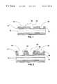
- FIG. 1is a cross-sectional view of a circuit board panel with two blind vias after laser drilling and a third blind via not yet laser drilled.
- FIG. 2is a cross-sectional view of a circuit board panel with blind vias for interconnections between layers 1 to 3 ; between layers 1 , 2 and 3 ; and between layers 1 to 2 .
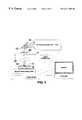
- FIG. 3is a schematic drawing of a preferred embodiment of the blind via laser drilling system of this invention, including lens configuration, motion control and laser firing control by glass scale positioning.
- FIG. 4is a schematic drawing of the lens positioning and focus point of the beam delivery system of FIG. 3 required for rapid laser beam pulse delivery.
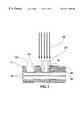
- FIG. 5is a cross-sectional view showing the watt density distribution that enters the etched window allowing the polymer dielectric material to be vaporized, forming a plateable blind via, in the method using the blind via laser drilling system of FIG. 3 .
- FIG. 6is a cross-sectional view of the flow of air and vacuum that enters the window during vaporizing which minimizes debris and charring in the method of this invention.
- FIG. 7is a cross-sectional view similar to FIG. 5 showing the oversize laser beam and reflected laser energy at both the base of the blind via and at the surface of the masked window.
- FIG. 8is a cross-sectional view of a resistive polymer being screened into a laser drilled blind via according to the method of this invention.
- FIG. 9is a flow diagram of the conventional sequential lamination process for producing mechanically drilled blind vias.
- FIG. 10is a flow diagram of the laser process according to the present invention and used with the laser system of FIG. 3 .
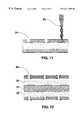
- FIG. 11is a cross sectional view of a mechanical drill that is drilled partly into the panel for controlled Z-Axis drilling.
- FIG. 12is a cross-sectional view of a conventional sequential lamination process for producing mechanically drilled blind vias.
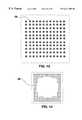
- FIG. 13is a ball grid array footprint on the surface of a circuit board panel with a laser drilled blind via in the center of each pad according to the invention.
- FIG. 14is a is a micro-ball grid array footprint on the surface of a circuit board panel with very small laser drilled blind vias in the center of each pad according to the invention.
- FIG. 15is a quad flat pack footprint on the surface of a circuit board panel with laser drilled blind vias in the center of each pad according to the invention.
- FIG. 16(top) is a plan view showing a Ball Grid Array and fine pitch Quad Flat Pack and traversal plan depicting the serpentine flow from the software optimization program for laser drilling the vias according to the invention.
- FIG. 17is an improved traversal plan after the use of software scripting to further optimize the travel path in the software optimization program.
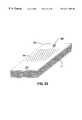
- FIG. 18is a perspective view of an off-contact slotted mask allowing a portion of the laser beam to be selectively directed to the etched windows according to the invention.
- FIG. 19is a drawing of the top of an off-contact slotted mask similar to that of FIG. 18 over an exhaust chamber for debris removal.
- FIG. 20is a drawing of a rectangular air nozzle system attached to the bottom view of the off-contact slotted mask.
- FIG. 21is a cross sectional view of the off-contact slotted mask with exhaust chamber.
- FIG. 22is a perspective view of a circuit board panel with an array of etched windows and two large etched windows at each end of the panel for theta alignment of the circuit board panel according to the invention.
- the dielectric materialhas not been laser drilled from within the two alignment windows.
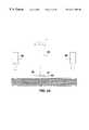
- FIG. 23is a cross sectional view of the panel of FIG. 2 with an alignment system according to the invention showing schematically two CCD cameras located at two preset tooling positions on either side of the laser beam delivery tube with the off-contact slotted mask and exhaust chamber on the bottom of the laser beam delivery tube.
- the dielectric material within the two alignment windowshave not been laser drilled.
- FIG. 24is a cross sectional view like FIG. 23 showing the laser beam delivery tube with the off-contact slotted mask and exhaust chamber on the bottom of the laser beam delivery tube aligned over one of the alignment windows.
- the dielectric material within the two alignment windowshas been laser drilled.
- FIG. 25is a perspective view similar to FIG. 23, but after the dielectric material has been laser drilled from within the two alignment windows to expose a buried pin on one of the inner layers.
- a laser systemis constructed by integrating a sufficiently powerful (preferably ⁇ 200 watts, more preferably 500 watts) sealed carbon dioxide (CO2) laser emitting an infrared (10.6 micrometer) laser beam pulsed by using radio frequency controls (RF excited) capable of pulse rates greater than 10,000 per second at a zero duty cycle.
- RF excitedradio frequency controls
- Synrad, Inc. of Mukilteo, Wash., U.S.A., and Coherent, Inc. of Santa Clara, Calif., U.S.A.make lasers that can be adapted as described herein.
- RF controlled CO2 lasershave been used in the medical profession because of the ability to rapidly pulse the laser beam and not appreciably harm tissue.
- This characteristiccan be transferred to laser drilling of polymers under controlled conditions as described in this invention. While the beam delivery rate of the RF controlled CO2 laser typically leaves less residue than the Continuous Wave (CW) CO2 laser systems, it does leave excess debris, fibers and charred polymer unless a high pressure stream of clean air is pointed into the blind via and extracted by a vacuum system. It was originally thought that inert gases such as Argon or Nitrogen were necessary to eliminate charring. Applicant's experiments have eliminated via wall charring by using clean high pressure air focused into the etched relief in the mask. The mechanism is believed to be similar to the effect of the air or oxygen blast in a acetylene cutting torch. Without this high stream of air the tapered walls are not concentric but oval.
- RF controlled CO2 lasers used in medical surgeryare typically less than 50 watts and not powerful enough to remove dielectric material. Furthermore, the laser beam in medical applications delivers multiple pulses in a focused fashion to remove tissue at the focal point making it economically impractical to rapidly remove dielectric materials in blind via circuit board applications. Even though sealed RF controlled CO2 lasers are available for industrial applications in the 200 to 700 watt range, a new laser system and processing method is needed to make drilling blind vias economically feasible.
- This inventioninvolves a moving laser beam delivery system that creates a watt density sufficiently strong enough, yet wide enough, to vaporize dielectric material through a window in a mask down to different depth blind pins 13 and 13 ′ with one pulse per via in a single pass. While the mechanism for removing dielectric material can be measured as Joules of energy, this invention allows for the delivery of a consistent energy level across the window opening, plus the energy level remains consistent down into the via. The key to doing this is to focus the beam well below the intended maximum depth of the via, preferably below the printed circuit thickness. The watt density of the beam into the dielectric material needs to be sufficiently strong enough to vaporize the polymer dielectric material but low enough not to harm the copper or other window mask surface 12 or the blind pin 16 and 16 ′. This invention allows multiple size etched windows or blind via diameters along with multiple depth blind vias to be produced with the same energy level without re-focus or pulse duration adjustment.
- FIG. 4depicts a long focal length lens 17 ranging from 127 mm to 254 mm when focused between 2.54 mm to about 50 mm below the top surface of the circuit board etched window 22 , changes the Gaussian curve for the beam creating a broad watt density curve 23 as shown in FIG. 5 .
- the amount of energy that is allowed to enter the etched windowis controlled by pulse duration. Pulse duration rates between 800 microseconds and 2,500 microseconds depend on the volume of dielectric material to be vaporized with a 200 watt sealed RF controlled CO2 laser with the ability to pulse at 10,000 per second (at zero duty cycle) can deliver between 1,250 vias per second and 400 vias per second. A 700 watt sealed RF controlled CO2 laser with the ability to pulse at 10,000 per second (at zero duty cycle) can deliver up to 3,000 vias per second.
- the inventionfurther embodies a useable beam at window entry 13 and 13 ′ that can be as large as three times the size of the etched window. This size will allow an effective 0.76 mm diameter wide beam to move rapidly and continuously over a 0.25 mm diameter etched window.
- the proper watt densityis controlled by the de-focus of the beam into the panel 22 and aided by the long focal length lens 17 .
- FIG. 7depicts the mechanism of beam overlap of etched window used within the invention for drilling-on-the-fly.
- the limitation on how small a diameter of the blind via can be produced by this inventionis governed by the ability to etch the appropriate window 13 and 13 ′ and its use as an interconnect is further limited by the processes that are used to make the blind vias conductive, such as electroless or direct plate and subsequent electroplating. These limitations are known and outside the scope of this invention.
- the tapered blind via wall 14is essential for the release of gasses that can be trapped in blind vias during the multiple steps in the metallization process.
- a vapor hone set at an appropriate pressure so as not damage the copper mask used in laser drillingcan be used to clean any fibers and condition the blind via for metallization.
- This vapor honeuses a slurry of 400 grit aluminum oxide under high air and water pressure to not only to clean the laser drilled blind vias, but also cleans any debris physically deposited on the surface around the windows 13 after laser drilling.
- Two manufacturers of vapor honesare Vapor Blast Mfg. Company and Pressure Blast Manufacturing Company.
- AOIAutomatic Optical Inspection
- An outgrowth of the economically drilled blind vias embodied in this inventionis the ability to screen 29 a resistive polymer 28 and 30 into a blind via that has been laser drilled to a diameter predetermined by the window size and a depth that can extend through multiple layers.
- a blind viatypically terminates at an internal ground plane as shown in FIG. 8 . Since these terminating blind vias 28 do not have to be plated, the window openings do not have any minimal size requirement. Therefore, via diameter and length as well as material resistivity can be used to control terminating resistance values. Terminating resistive polymer materials that are used in the ceramic hybrid circuit industry are available for the laser drilled terminating resistor.
- the cost effective laser drilled blind vias produced by this inventionmay be used to produce terminating resistors on the surface of the panel as shown in FIG. 8 .
- Windows etched for this featureare calculated by understanding the volume of resistive material, but primary resistance control is within the mixture of the polymer resist 30 .
- Two methodsmay be used to deposit the resistive material into the laser drilled blind vias.
- One methodis to flood the surface with resistive material and squeegee 29 this material into the laser drilled blind vias by dragging a hard sharp squeegee over the entire surface.
- a second methodwould to use a screen with relief openings over the laser drilled vias 31 that would allow the resistive polymer to selectively enter the vias defined as terminating resistors.
- the second methodwould allow all the blind vias to be laser drilled at the same time.
- the blind vias selected to be conductivewould be masked by the screen as the terminating resistor vias are filled with polymer material.
- a off-contact slotted mask 39 as shown in FIG. 18allows a slotted section of the beam 20 to pass through the slot 40 .
- the slotted maskis made of a material that will absorb that portion of the laser beam that does not pass through the slot.
- the resulting elongated narrow beamcan now be rapidly move in the direction of its longest opening allowing the laser beam to be pulsed over an row of etched windows.
- This maskallows the defocused beam used in the present invention to travel in one axis without hitting a nearby row of etched windows.
- the panelis moved under the slotted mask 39 in one axis, then the slotted mask, or the X/Y table, is rotated 90 degrees and the table with the panel is moved in the opposite axis.
- the off-contact slotted maskis made of a sufficiently thick metal, preferably Aluminum, to absorb the defocused beam without creating an absorbed temperature to distort the mask.
- Refrigeration coolingmay be used to cooling the off-contact slotted mask by running the heat exchanged coolant from the RF Power Supplies and RF Excited CO2 laser.
- the pre-optimized travel pathis set to move the table in one axis at a time with the laser beam pulsed at the appropriate pulse duration (e.g., 0.0005 sec. to 0.003 sec for nonwoven aramid dielectric of thickness ranging from 0.05 mm to 0.2 mm).
- the table speed for a given pulse durationis calculated for the diameter of the etched window 12 and the dielectric thickness 11 (e.g., 760 mm/sec to 250 mm/sec for a 200 watt laser).
- a disbursement of clean dry air as in FIG. 6is delivered in the slotted mask 39 of FIG. 20 to the rectangular via cleaning attachment 43 so that a force of clean dry air is jettisoned into the etched windows 12 while the laser beam is pulsed.
- the airacts like the heavy gas flow in a cutting torch and forces debris and other materials from the laser drilled etched windows 13 and 13 ′, resulting in a laser drilled blind via that will not need to be post cleaned or will need very little post cleaning.
- a small chamber used for exhaust and debris removalis just below the slotted mask 39 and the air jet rectangular via cleaning attachment 43 .
- Registration and theta alignmentcan be accomplished as shown in FIGS. 23 and 24 by moving the panel under to preset CCD Alignment cameras 49 and 49 ′ allowing a rotating theta table to move the panel over or under the X/Y table.
- the two large etched windows 45 at each end of the panel, shown in FIG. 22,can be used to average the registration through currently available software and vision hardware.
- the tableis moved under the laser beam delivery tube 48 as shown in FIG. 24, and the laser is pulsed with a long enough pulse duration to remove the dielectric material as shown in FIG. 25, exposing a buried pin 47 .
- This buried pincan be the same etched spot that is used by many circuit board fabricators for inner layer alignment in the MultiLine Four Slot System.
- buried pinsmay be used as buried pins for alignment.
- the tablemay move the panels back under the CCD Cameras (or a camera with beam-splitter mirrors) as shown in FIG. 23 (without dielectric material removed) and a quality check can occur. If the buried pin 47 is located within a tolerable range within the laser drilled etched window 46 , the panel can be aligned to the first etched blind via window for the circuit design and laser drilling can commence. If the buried pin 47 is outside a tolerable range within the laser drilled tooling etched windows 46 the panel may be rejected and removed from the system. Theta alignment using two pins 47 thus provides an optical alignment technique that enables the laser drilling process to be moved rapidly along a traverse in a single axis.
- the focal length of the focusing lens 17is shown as an unknown distance 21 from the top of work piece 9 .
- This focal length of the focusing lensis critical to allow an appropriate watt density distribution 23 as shown in FIG. 5, making it possible to single pulse the laser system in a rapid fashion and remove the polymer dielectric material 11 .
- the tapered blind via wall 14(FIGS. 1 and 2) is essential for making the blind via conductive by first electroless or direct plate and subsequent electrolytic plating methods, especially in multi-level interconnects.
- off-contact slotted mask 39 in FIGS. 18, 19 , 20 and 21allows a further enlarged beam to be used.
- the laser systemneeds the following five key electronically controlled elements in order to drill cost effectively:
- the laseris controlled by electronics in the laser control box which takes positional information received from the computer and coordinates firing of the laser with positioning of the table.
- the tableis driven by the control box and a set of glass scales on the table, with which the board 9 is aligned to a known position, are monitored optically to determine anticipatorily when the laser should be fired. This alignment and control technique allows faster movement with accuracy between drilling positions than the galvanometer and table combination used by other laser drilling systems.
- the laser beam 20is rapidly pulsed just prior to or just as it enters the window 12 on the panel as shown is FIG. 7 .
- the natural reflection of laser beam 27 from the copper mask 16 on the surface and from the base 16 ′ of the blind viaare made possible by the low watt density of the defocused laser beam 20 and the wavelength of the sealed RF controlled CO2 laser.
- the invention described in the embodied system integrationallows the table to move in a continuous motion which is defined as true drill-on-the-fly.
- the inventioncreates the capability of accurately delivering a single pulse laser beam into the respective windows 12 to drill vias at a very high speed.
- the rate at which via can be drilledis only limited by the maximum rate of the pulsed beam 20 leaving the laser aperture 19 and the average speed of the Motion Positioning Table.
- the Maximum Panels per Dayis calculated on a 20 hour operating day (3 shifts) with 20,000 vias per panels plus a 15 second per panel handling time ranges from 1500 to 3000 panels per day with via drilled at 0.32 mm centers for dielectric thicknesses of 0.2 mm to 0.05 mm.
- production rates for an Nd:YAG laser (266 nm) having a beam diameter of 0.1 mmwould be more than an order of magnitude loss due to the need to trepan the larger vias.
- the Nd:YAGmust be multiple-pulse for thicker dielectrics, >0.09 mm, precluding high-speed on-the-fly drilling.
- the estimated maximum output in VIAS PER SECOND for laser blind via drilling with the system embodied within this disclosureusing epoxy or polyimide non-woven aramid dielectric and a laser beam width of 0.762 mm in diameter for a 500 watt RF Excited CO2 sealed laser by Synrad, Inc.
- the beam diametermay change to accomplish the appropriate energy range for removing various dielectric materials along with lens variations.
Landscapes
- Engineering & Computer Science (AREA)
- Physics & Mathematics (AREA)
- Optics & Photonics (AREA)
- Plasma & Fusion (AREA)
- Mechanical Engineering (AREA)
- Manufacturing & Machinery (AREA)
- Microelectronics & Electronic Packaging (AREA)
- Laser Beam Processing (AREA)
Abstract
Description
Claims (20)
Priority Applications (3)
| Application Number | Priority Date | Filing Date | Title |
|---|---|---|---|
| US09/194,933US6211485B1 (en) | 1996-06-05 | 1997-06-05 | Blind via laser drilling system |
| US09/823,217US6631558B2 (en) | 1996-06-05 | 2001-03-30 | Blind via laser drilling system |
| US10/389,544US7062845B2 (en) | 1996-06-05 | 2003-03-14 | Conveyorized blind microvia laser drilling system |
Applications Claiming Priority (3)
| Application Number | Priority Date | Filing Date | Title |
|---|---|---|---|
| US1914096P | 1996-06-05 | 1996-06-05 | |
| PCT/US1997/009732WO1997046349A1 (en) | 1996-06-05 | 1997-06-05 | Blind via laser drilling system |
| US09/194,933US6211485B1 (en) | 1996-06-05 | 1997-06-05 | Blind via laser drilling system |
Related Parent Applications (1)
| Application Number | Title | Priority Date | Filing Date |
|---|---|---|---|
| PCT/US1997/009732Continuation-In-PartWO1997046349A1 (en) | 1996-06-05 | 1997-06-05 | Blind via laser drilling system |
Related Child Applications (1)
| Application Number | Title | Priority Date | Filing Date |
|---|---|---|---|
| US09/823,217Continuation-In-PartUS6631558B2 (en) | 1996-06-05 | 2001-03-30 | Blind via laser drilling system |
Publications (1)
| Publication Number | Publication Date |
|---|---|
| US6211485B1true US6211485B1 (en) | 2001-04-03 |
Family
ID=21791652
Family Applications (1)
| Application Number | Title | Priority Date | Filing Date |
|---|---|---|---|
| US09/194,933Expired - LifetimeUS6211485B1 (en) | 1996-06-05 | 1997-06-05 | Blind via laser drilling system |
Country Status (3)
| Country | Link |
|---|---|
| US (1) | US6211485B1 (en) |
| AU (1) | AU3301197A (en) |
| WO (1) | WO1997046349A1 (en) |
Cited By (83)
| Publication number | Priority date | Publication date | Assignee | Title |
|---|---|---|---|---|
| US6433303B1 (en)* | 2000-03-31 | 2002-08-13 | Matsushita Electric Industrial Co., Ltd. | Method and apparatus using laser pulses to make an array of microcavity holes |
| US20020167581A1 (en)* | 2001-03-29 | 2002-11-14 | Cordingley James J. | Methods and systems for thermal-based laser processing a multi-material device |
| US6492616B1 (en)* | 1999-05-24 | 2002-12-10 | Nippon Steel Chemical Co., Ltd. | Processes for laser beam machining of resin film for wiring boards and manufacture of wiring boards |
| US20020185474A1 (en)* | 2001-05-09 | 2002-12-12 | Dunsky Corey M. | Micromachining with high-energy, intra-cavity Q-switched CO2 laser pulses |
| US20030000930A1 (en)* | 2000-01-28 | 2003-01-02 | Shiro Hamada | Laser machining device and laser machining mask and production method therefor |
| US20030151053A1 (en)* | 2000-01-10 | 2003-08-14 | Yunlong Sun | Processing a memory link with a set of at least two laser pulses |
| US20030201258A1 (en)* | 2002-04-30 | 2003-10-30 | Hubert De Steur | Method for producing a trench structure in a polymer substrate |
| US20030201578A1 (en)* | 2002-04-26 | 2003-10-30 | Ming Li | Method of drilling holes with precision laser micromachining |
| US20030222324A1 (en)* | 2000-01-10 | 2003-12-04 | Yunlong Sun | Laser systems for passivation or link processing with a set of laser pulses |
| US20040004061A1 (en)* | 2002-07-03 | 2004-01-08 | Merdan Kenneth M. | Tubular cutting process and system |
| US20040134896A1 (en)* | 1999-12-28 | 2004-07-15 | Bo Gu | Laser-based method and system for memory link processing with picosecond lasers |
| US20040134894A1 (en)* | 1999-12-28 | 2004-07-15 | Bo Gu | Laser-based system for memory link processing with picosecond lasers |
| US20040173589A1 (en)* | 2003-03-05 | 2004-09-09 | Kam-Chuen Yung | Method of drilling a circuit board |
| US20040188393A1 (en)* | 2002-12-24 | 2004-09-30 | Ming Li | Method and apparatus of drilling high density submicron cavities using parallel laser beams |
| US20040188399A1 (en)* | 1999-12-28 | 2004-09-30 | Gsi Lumonics Inc. | Energy-efficient, laser-based method and system for processing target material |
| US20040222197A1 (en)* | 1996-11-20 | 2004-11-11 | Ibiden Co., Ltd. | Laser machining apparatus, and apparatus and method for manufacturing a multilayered printed wiring board |
| US20040223698A1 (en)* | 2003-05-06 | 2004-11-11 | Lockheed Martin Corporation | Active optical alignment of laser diode array for drilling precising holes |
| US20040226745A1 (en)* | 1999-08-06 | 2004-11-18 | Ibiden Co., Ltd. | Electroplating solution, method for manufacturing multilayer printed circuit board using the same solution, and multilayer printed circuit board |
| US6863936B2 (en)* | 2000-12-19 | 2005-03-08 | Agency For Science, Technology And Research | Method of forming selective electroless plating on polymer surfaces |
| US6888096B1 (en)* | 1999-09-28 | 2005-05-03 | Sumitomo Heavy Industries, Ltd. | Laser drilling method and laser drilling device |
| US20050098548A1 (en)* | 2003-11-06 | 2005-05-12 | Satoshi Kobayashi | Processing apparatus using laser beam |
| US6898358B2 (en) | 2002-05-31 | 2005-05-24 | Matsushita Electric Industrial Co., Ltd. | Adjustable photonic crystal and method of adjusting the index of refraction of photonic crystals to reversibly tune transmissions within the bandgap |
| US20050136646A1 (en)* | 2003-12-18 | 2005-06-23 | Endicott Interconnect Technologies, Inc. | Method of providing printed circuit board with conductive holes and board resulting therefrom |
| US20050218126A1 (en)* | 2002-06-19 | 2005-10-06 | Frewitt Printing Sa | Method and a device for depositing a wipe-proof and rub-proof marking onto transparent glass |
| US20050263498A1 (en)* | 1996-11-20 | 2005-12-01 | Ibiden Co., Ltd. | Ceramic heater |
| US20060070982A1 (en)* | 2003-05-30 | 2006-04-06 | Patel Arvindbhai L | Novel laser bruting machine |
| US20060141681A1 (en)* | 2000-01-10 | 2006-06-29 | Yunlong Sun | Processing a memory link with a set of at least two laser pulses |
| US20070106416A1 (en)* | 2006-06-05 | 2007-05-10 | Griffiths Joseph J | Method and system for adaptively controlling a laser-based material processing process and method and system for qualifying same |
| US20070199927A1 (en)* | 1999-12-28 | 2007-08-30 | Bo Gu | Laser-based method and system for removing one or more target link structures |
| US20070278703A1 (en)* | 2006-06-02 | 2007-12-06 | Electro Scientific Industries, Inc. | Process for structurally thinning materials drilled with via patterns |
| US20070291496A1 (en)* | 2006-06-02 | 2007-12-20 | Electro Scientific Industries, Inc. | Process for optically transparent via filling |
| US20080011715A1 (en)* | 2006-07-11 | 2008-01-17 | Electro Scientific Industies, Inc. | Process and system for quality management and analysis of via drilling |
| WO2007142909A3 (en)* | 2006-06-02 | 2008-10-23 | Electro Scient Ind Inc | Process for optically transparent via filling |
| US20080268553A1 (en)* | 2007-04-27 | 2008-10-30 | Cheng Hsun Chan | Electroless plating apparatus with non-liquid heating source |
| US20080289178A1 (en)* | 2007-05-25 | 2008-11-27 | Electro Scientific Industries, Inc. | Process for forming an isolated electrically conductive contact through a metal package |
| US20080296273A1 (en)* | 2007-06-01 | 2008-12-04 | Electro Scientific Industries, Inc. | Method of and apparatus for laser drilling holes with improved taper |
| US20090001550A1 (en)* | 2007-06-28 | 2009-01-01 | Yonggang Li | Method of Forming a Multilayer Substrate Core Structure Using Sequential Microvia Laser Drilling And Substrate Core Structure Formed According to the Method |
| US20090002958A1 (en)* | 2007-06-28 | 2009-01-01 | Yonggang Li | Method of Forming a Substrate Core Structure Using Microvia Laser Drilling and Conductive Layer Pre-Patterning And Substrate Core Structure Formed According to the Method |
| CN100455163C (en)* | 2005-06-14 | 2009-01-21 | 南亚电路板股份有限公司 | Manufacturing method of printed circuit board |
| US20090053459A1 (en)* | 1998-12-16 | 2009-02-26 | Ibiden Co., Ltd. | Conductive connecting pin and package substrate |
| US20090057279A1 (en)* | 2007-08-31 | 2009-03-05 | Rolls-Royce Plc | Method of cutting with a laser |
| US20090194516A1 (en)* | 2005-02-03 | 2009-08-06 | Laserfacturing Inc. | Method and apparatus for via drilling and selective material removal using an ultrafast pulse laser |
| US20090242528A1 (en)* | 2008-03-27 | 2009-10-01 | Electro Scientific Industries, Inc. | Method and apparatus for laser drilling holes with gaussian pulses |
| US20090312859A1 (en)* | 2008-06-16 | 2009-12-17 | Electro Scientific Industries, Inc. | Modifying entry angles associated with circular tooling actions to improve throughput in part machining |
| US7638732B1 (en)* | 2002-10-24 | 2009-12-29 | Analogic Corporation | Apparatus and method for making X-ray anti-scatter grid |
| US20100044092A1 (en)* | 2008-08-20 | 2010-02-25 | Electro Scientific Industries, Inc. | Method and apparatus for optically transparent via filling |
| US20100126975A1 (en)* | 2008-11-21 | 2010-05-27 | Tesa Se | Method of Working Material with High-Energy Radiation |
| US20110147056A1 (en)* | 2009-12-17 | 2011-06-23 | Unimicron Technology Corp. | Circuit board and process for fabricating the same |
| US20110236645A1 (en)* | 2010-03-26 | 2011-09-29 | Electro Scientific Industries, Inc. | Method of manufacturing a panel with occluded microholes and products made thereby |
| WO2011000814A3 (en)* | 2009-06-29 | 2012-03-08 | Reis Group Holding Gmbh & Co. Kg | Method for exposing an electrical contact |
| US20120217230A1 (en)* | 2003-08-11 | 2012-08-30 | David Gaudiosi | Methods and systems for trimming circuits |
| US8884184B2 (en) | 2010-08-12 | 2014-11-11 | Raydiance, Inc. | Polymer tubing laser micromachining |
| US20140353295A1 (en)* | 2013-05-29 | 2014-12-04 | Regent Technologies Limited | System, method and apparatus for removing a burr from a slotted pipe |
| US9114482B2 (en) | 2010-09-16 | 2015-08-25 | Raydiance, Inc. | Laser based processing of layered materials |
| CN105376941A (en)* | 2015-11-02 | 2016-03-02 | 深圳市五株科技股份有限公司 | Printed circuit board processing method |
| US9812386B1 (en) | 2002-05-01 | 2017-11-07 | Amkor Technology, Inc. | Encapsulated semiconductor package |
| US10239160B2 (en) | 2011-09-21 | 2019-03-26 | Coherent, Inc. | Systems and processes that singulate materials |
| US10811277B2 (en) | 2004-03-23 | 2020-10-20 | Amkor Technology, Inc. | Encapsulated semiconductor package |
| US20210114072A1 (en)* | 2016-11-23 | 2021-04-22 | Aperam | Method for laser stripping a moving metal product and plant for the execution thereof |
| US20210121979A1 (en)* | 2019-10-24 | 2021-04-29 | Samsung Display Co., Ltd. | Substrate processing apparatus and method |
| US11081370B2 (en) | 2004-03-23 | 2021-08-03 | Amkor Technology Singapore Holding Pte. Ltd. | Methods of manufacturing an encapsulated semiconductor device |
| US11094560B1 (en) | 2004-03-23 | 2021-08-17 | Amkor Technology Singapore Holding Pte. Ltd. | Encapsulated semiconductor package |
| CN113543479A (en)* | 2020-04-20 | 2021-10-22 | 无锡深南电路有限公司 | Ultrathin circuit board and preparation method thereof |
| US11232951B1 (en) | 2020-07-14 | 2022-01-25 | Applied Materials, Inc. | Method and apparatus for laser drilling blind vias |
| CN113977113A (en)* | 2021-11-30 | 2022-01-28 | 重庆川仪自动化股份有限公司 | Processing method for blind hole of gem measuring head |
| US11264333B2 (en) | 2019-05-10 | 2022-03-01 | Applied Materials, Inc. | Reconstituted substrate structure and fabrication methods for heterogeneous packaging integration |
| CN114222432A (en)* | 2021-12-28 | 2022-03-22 | 江西志浩电子科技有限公司 | A Processing Technology of Skip Via Laser Drilling |
| US11342256B2 (en) | 2019-01-24 | 2022-05-24 | Applied Materials, Inc. | Method of fine redistribution interconnect formation for advanced packaging applications |
| US11362235B2 (en) | 2019-05-10 | 2022-06-14 | Applied Materials, Inc. | Substrate structuring methods |
| CN114745871A (en)* | 2022-03-21 | 2022-07-12 | 江西福昌发电路科技有限公司 | A laser drilling ash removal process for HDI circuit board production |
| US11400545B2 (en) | 2020-05-11 | 2022-08-02 | Applied Materials, Inc. | Laser ablation for package fabrication |
| US11404318B2 (en) | 2020-11-20 | 2022-08-02 | Applied Materials, Inc. | Methods of forming through-silicon vias in substrates for advanced packaging |
| US11454884B2 (en) | 2020-04-15 | 2022-09-27 | Applied Materials, Inc. | Fluoropolymer stamp fabrication method |
| US11521937B2 (en) | 2020-11-16 | 2022-12-06 | Applied Materials, Inc. | Package structures with built-in EMI shielding |
| CN115460773A (en)* | 2022-07-26 | 2022-12-09 | 德中(天津)技术发展股份有限公司 | Method, software and equipment for manufacturing circuit board by laser manufacturing opening transfer material |
| CN116113152A (en)* | 2021-11-09 | 2023-05-12 | 三星电机株式会社 | Printed circuit board with improved heat dissipation |
| US11676832B2 (en) | 2020-07-24 | 2023-06-13 | Applied Materials, Inc. | Laser ablation system for package fabrication |
| US11705365B2 (en) | 2021-05-18 | 2023-07-18 | Applied Materials, Inc. | Methods of micro-via formation for advanced packaging |
| US11742330B2 (en) | 2020-03-10 | 2023-08-29 | Applied Materials, Inc. | High connectivity device stacking |
| US11862546B2 (en) | 2019-11-27 | 2024-01-02 | Applied Materials, Inc. | Package core assembly and fabrication methods |
| US11931855B2 (en) | 2019-06-17 | 2024-03-19 | Applied Materials, Inc. | Planarization methods for packaging substrates |
| US12183684B2 (en) | 2021-10-26 | 2024-12-31 | Applied Materials, Inc. | Semiconductor device packaging methods |
| WO2025010929A1 (en)* | 2023-07-11 | 2025-01-16 | 赣州市超跃科技股份有限公司 | Quality control system, method and device for high-density circuit board, and medium |
Families Citing this family (5)
| Publication number | Priority date | Publication date | Assignee | Title |
|---|---|---|---|---|
| GB9811557D0 (en)* | 1998-05-29 | 1998-07-29 | Exitech Ltd | The use of beam shaping for improving the performance of machines used to laser drill microvia holes in printed circuit (wiring) and other packages |
| GB2433460A (en)* | 2005-12-20 | 2007-06-27 | Arisawa Seisakusho Kk | Laser ablation apparatus,processing method and mask therefor |
| CN101986770B (en)* | 2010-08-06 | 2013-04-03 | 深圳崇达多层线路板有限公司 | Multi-order high-density circuit board registration hole and manufacturing method thereof |
| CN105499820A (en)* | 2016-01-12 | 2016-04-20 | 武汉华星光电技术有限公司 | Automatic welding system for flexible printed circuit board |
| CN112654164A (en)* | 2020-12-25 | 2021-04-13 | 悦虎晶芯电路(苏州)股份有限公司 | Blind hole and circuit pattern high-precision alignment mode |
Citations (18)
| Publication number | Priority date | Publication date | Assignee | Title |
|---|---|---|---|---|
| US4500389A (en) | 1981-04-14 | 1985-02-19 | Kollmorgen Technologies Corporation | Process for the manufacture of substrates to interconnect electronic components |
| US4504727A (en) | 1982-12-30 | 1985-03-12 | International Business Machines Corporation | Laser drilling system utilizing photoacoustic feedback |
| US4544442A (en) | 1981-04-14 | 1985-10-01 | Kollmorgen Technologies Corporation | Process for the manufacture of substrates to interconnect electronic components |
| US4606747A (en) | 1981-11-14 | 1986-08-19 | Schott-Zwiesel-Glaswerke Ag | Process for the contact-less removal of material from the surface of a glass object |
| US4642160A (en) | 1985-08-12 | 1987-02-10 | Interconnect Technology Inc. | Multilayer circuit board manufacturing |
| US4644130A (en) | 1984-05-18 | 1987-02-17 | Siemens Aktiengesellschaft | Method for creating blind holes in a laminated structure |
| US4764485A (en) | 1987-01-05 | 1988-08-16 | General Electric Company | Method for producing via holes in polymer dielectrics |
| US4789770A (en)* | 1987-07-15 | 1988-12-06 | Westinghouse Electric Corp. | Controlled depth laser drilling system |
| JPH02147182A (en) | 1988-11-29 | 1990-06-06 | Nec Corp | Laser beam trimming device |
| JPH02192885A (en) | 1989-01-20 | 1990-07-30 | Tdk Corp | Laser beam processor |
| US5010232A (en) | 1989-01-27 | 1991-04-23 | Hitachi Seiko, Ltd. | Method of and apparatus for perforating printed circuit board |
| US5087396A (en) | 1988-09-15 | 1992-02-11 | Unisys Corporation | Method of forming holes in unfired ceramic layers of integrated circuit packages |
| US5108785A (en)* | 1989-09-15 | 1992-04-28 | Microlithics Corporation | Via formation method for multilayer interconnect board |
| US5173442A (en)* | 1990-07-23 | 1992-12-22 | Microelectronics And Computer Technology Corporation | Methods of forming channels and vias in insulating layers |
| US5367143A (en) | 1992-12-30 | 1994-11-22 | International Business Machines Corporation | Apparatus and method for multi-beam drilling |
| US5378869A (en) | 1992-06-02 | 1995-01-03 | Amkor Electronics, Inc. | Method for forming an integrated circuit package with via interconnection |
| US5844200A (en)* | 1996-05-16 | 1998-12-01 | Sendex Medical, Inc. | Method for drilling subminiature through holes in a sensor substrate with a laser |
| US6107003A (en)* | 1998-01-14 | 2000-08-22 | Mitsui Mining & Smelting Co., Ltd. | Method for producing multi-layer printed wiring boards having blind vias |
Family Cites Families (1)
| Publication number | Priority date | Publication date | Assignee | Title |
|---|---|---|---|---|
| JPS61229492A (en)* | 1985-04-03 | 1986-10-13 | Hitachi Ltd | How to form through holes in a substrate |
- 1997
- 1997-06-05USUS09/194,933patent/US6211485B1/ennot_activeExpired - Lifetime
- 1997-06-05AUAU33011/97Apatent/AU3301197A/ennot_activeAbandoned
- 1997-06-05WOPCT/US1997/009732patent/WO1997046349A1/enactiveApplication Filing
Patent Citations (18)
| Publication number | Priority date | Publication date | Assignee | Title |
|---|---|---|---|---|
| US4544442A (en) | 1981-04-14 | 1985-10-01 | Kollmorgen Technologies Corporation | Process for the manufacture of substrates to interconnect electronic components |
| US4500389A (en) | 1981-04-14 | 1985-02-19 | Kollmorgen Technologies Corporation | Process for the manufacture of substrates to interconnect electronic components |
| US4606747A (en) | 1981-11-14 | 1986-08-19 | Schott-Zwiesel-Glaswerke Ag | Process for the contact-less removal of material from the surface of a glass object |
| US4504727A (en) | 1982-12-30 | 1985-03-12 | International Business Machines Corporation | Laser drilling system utilizing photoacoustic feedback |
| US4644130A (en) | 1984-05-18 | 1987-02-17 | Siemens Aktiengesellschaft | Method for creating blind holes in a laminated structure |
| US4642160A (en) | 1985-08-12 | 1987-02-10 | Interconnect Technology Inc. | Multilayer circuit board manufacturing |
| US4764485A (en) | 1987-01-05 | 1988-08-16 | General Electric Company | Method for producing via holes in polymer dielectrics |
| US4789770A (en)* | 1987-07-15 | 1988-12-06 | Westinghouse Electric Corp. | Controlled depth laser drilling system |
| US5087396A (en) | 1988-09-15 | 1992-02-11 | Unisys Corporation | Method of forming holes in unfired ceramic layers of integrated circuit packages |
| JPH02147182A (en) | 1988-11-29 | 1990-06-06 | Nec Corp | Laser beam trimming device |
| JPH02192885A (en) | 1989-01-20 | 1990-07-30 | Tdk Corp | Laser beam processor |
| US5010232A (en) | 1989-01-27 | 1991-04-23 | Hitachi Seiko, Ltd. | Method of and apparatus for perforating printed circuit board |
| US5108785A (en)* | 1989-09-15 | 1992-04-28 | Microlithics Corporation | Via formation method for multilayer interconnect board |
| US5173442A (en)* | 1990-07-23 | 1992-12-22 | Microelectronics And Computer Technology Corporation | Methods of forming channels and vias in insulating layers |
| US5378869A (en) | 1992-06-02 | 1995-01-03 | Amkor Electronics, Inc. | Method for forming an integrated circuit package with via interconnection |
| US5367143A (en) | 1992-12-30 | 1994-11-22 | International Business Machines Corporation | Apparatus and method for multi-beam drilling |
| US5844200A (en)* | 1996-05-16 | 1998-12-01 | Sendex Medical, Inc. | Method for drilling subminiature through holes in a sensor substrate with a laser |
| US6107003A (en)* | 1998-01-14 | 2000-08-22 | Mitsui Mining & Smelting Co., Ltd. | Method for producing multi-layer printed wiring boards having blind vias |
Non-Patent Citations (13)
| Title |
|---|
| Cable, Alan, New Laser Processes and Wavelengths for Drilling Through-vias and Blind Vias in a Wide Range of Circuit Board Materials, IPC Expo, Proceeding of the Technical Conference, Mar. 1996, pp. S18, 5, 1-S18,5,9. |
| Carpenter et al., Richard, SLC: An organic Packaging Soluction for the Year 2000, IPC Expo, Proceeding of the Technical Conference, Mar. 1996, pp. S14, 2, I-S14, 2,6. |
| D'Ambra et al., Via formation in green ceramic dielectrics using a YAG laser, IEEE Electronic Components and Technology Conference. New York: IEEE, 1992, pp. 1072-1081, especially p. 1078 and Fig. 7. |
| Grace, Jim et al., Fulfilling the Demand for Greater Circuit Densities, CircuiTree, Jun. 1992, pp. 24-26. |
| Grace, Jim, Achieving Higher Circuit Densities Through Cost-Effective Blind Vias, Electronic Packaging & Production, Jun. 1993, pp. 46-48. |
| Hecht, Jeff, The Laser Guidebook, New York: McGraw-Hill, 1992, pp. 161-167, especially p. 163. |
| Hodson, Timothy L., Using Laser-Drilled Blind Vias to Maximize Board Capacity, Electronic Packaging & Production, Mar. 1992, p. 83. |
| Kestenbaum, et al., Laser Drilling of Microvias in Epoxy-Glass Printed Circuit Boards, IEEE Transaction on Components, Hybrids, and Manufacturing Tech., Dec. 1990, vol. 13, No. 4, pp. 1055-1062, especially Fig. 10 and p. 1061. |
| Maliniak, David, On the Road(map): Interconnects Face The Future, Electronic Design, Oct. 13, 1995, pp. 77-78; 80; 82; 84-85. |
| Murray, Jerry, At Double Header, Printed Circuit Fabrication, May 1996, p. 64. |
| Oxford, Rex, Plasma Formed Microvias for Future High Density Interconnects, IPC Expo, Proceeding of the Technical Conference, Mar. 1996, pp. S14, 3, 1-S14, 3,2. |
| Powell, David J., High Speed Laser Ablation of Microvia Holes in Nonwoven Aramid Reinforced Printed Wiring Boards to Reduce Cost, IPC Expo, Proceeding of the Technical Conference, Mar. 1996, pp. S18, 3, 1-S18,3,11. |
| Tourne, Joan, Microvias, a New Cost-Effective Interconnection Technology, IPC Expo, Proceeding of the Technical Conference, Mar. 1996, pp. S18, 4,1-S18,4,4. |
Cited By (208)
| Publication number | Priority date | Publication date | Assignee | Title |
|---|---|---|---|---|
| US7732732B2 (en)* | 1996-11-20 | 2010-06-08 | Ibiden Co., Ltd. | Laser machining apparatus, and apparatus and method for manufacturing a multilayered printed wiring board |
| US20060138098A1 (en)* | 1996-11-20 | 2006-06-29 | Ibiden Co., Ltd. | Laser machining apparatus, and apparatus and method for manufacturing a multilayered printed wiring board |
| US20050263498A1 (en)* | 1996-11-20 | 2005-12-01 | Ibiden Co., Ltd. | Ceramic heater |
| US7456372B2 (en) | 1996-11-20 | 2008-11-25 | Ibiden Co., Ltd. | Laser machining apparatus, and apparatus and method for manufacturing a multilayered printed wiring board |
| US7462802B2 (en) | 1996-11-20 | 2008-12-09 | Ibiden Co., Ltd. | Laser machining apparatus, and apparatus and method for manufacturing a multilayered printed wiring board |
| US7462801B1 (en) | 1996-11-20 | 2008-12-09 | Ibiden Co., Ltd. | Laser machining apparatus, and apparatus and method for manufacturing a multilayered printed wiring board |
| US20060138097A1 (en)* | 1996-11-20 | 2006-06-29 | Ibiden Co., Ltd. | Laser machining apparatus, and apparatus and method for manufacturing a multilayered printed wiring board |
| US7667160B2 (en) | 1996-11-20 | 2010-02-23 | Ibiden Co., Ltd | Laser machining apparatus, and apparatus and method for manufacturing a multilayered printed wiring board |
| US20040222197A1 (en)* | 1996-11-20 | 2004-11-11 | Ibiden Co., Ltd. | Laser machining apparatus, and apparatus and method for manufacturing a multilayered printed wiring board |
| US20090053459A1 (en)* | 1998-12-16 | 2009-02-26 | Ibiden Co., Ltd. | Conductive connecting pin and package substrate |
| US8035214B1 (en) | 1998-12-16 | 2011-10-11 | Ibiden Co., Ltd. | Conductive connecting pin for package substance |
| US8536696B2 (en) | 1998-12-16 | 2013-09-17 | Ibiden Co., Ltd. | Conductive pin attached to package substrate |
| US8110917B2 (en) | 1998-12-16 | 2012-02-07 | Ibiden Co., Ltd. | Package substrate with a conductive connecting pin |
| US20090154131A1 (en)* | 1998-12-16 | 2009-06-18 | Ibiden Co., Ltd. | Conductive connecting pin and package substrate |
| US20090314537A1 (en)* | 1998-12-16 | 2009-12-24 | Ibiden Co., Ltd. | Conductive connecting pin and package substrate |
| US20100032200A1 (en)* | 1998-12-16 | 2010-02-11 | Ibiden Co., Ltd. | Conductive connecting pin and package substrate |
| US7902659B2 (en)* | 1998-12-16 | 2011-03-08 | Ibiden Co., Ltd. | Conductive connecting pin and package substrate |
| US7847393B2 (en) | 1998-12-16 | 2010-12-07 | Ibiden Co., Ltd. | Conductive connecting pins for a package substrate |
| US6492616B1 (en)* | 1999-05-24 | 2002-12-10 | Nippon Steel Chemical Co., Ltd. | Processes for laser beam machining of resin film for wiring boards and manufacture of wiring boards |
| US7514637B1 (en) | 1999-08-06 | 2009-04-07 | Ibiden Co., Ltd. | Electroplating solution, method for fabricating multilayer printed wiring board using the solution, and multilayer printed wiring board |
| US20040226745A1 (en)* | 1999-08-06 | 2004-11-18 | Ibiden Co., Ltd. | Electroplating solution, method for manufacturing multilayer printed circuit board using the same solution, and multilayer printed circuit board |
| US7446263B2 (en)* | 1999-08-06 | 2008-11-04 | Ibiden Co., Ltd. | Multilayer printed circuit board |
| US7812262B2 (en) | 1999-08-06 | 2010-10-12 | Ibiden Co., Ltd. | Multilayer printed circuit board |
| US7993510B2 (en) | 1999-08-06 | 2011-08-09 | Ibiden Co., Ltd. | Electroplating solution, method for manufacturing multilayer printed circuit board using the same solution, and multilayer printed circuit board |
| US6888096B1 (en)* | 1999-09-28 | 2005-05-03 | Sumitomo Heavy Industries, Ltd. | Laser drilling method and laser drilling device |
| US7838794B2 (en) | 1999-12-28 | 2010-11-23 | Gsi Group Corporation | Laser-based method and system for removing one or more target link structures |
| US7750268B2 (en) | 1999-12-28 | 2010-07-06 | Gsi Group Corporation | Energy efficient, laser-based method and system for processing target material |
| US7582848B2 (en) | 1999-12-28 | 2009-09-01 | Gsi Group Corp | Energy-efficient, laser-based method and system for processing target material |
| US7679030B2 (en) | 1999-12-28 | 2010-03-16 | Gsi Group Corporation | Energy-efficient, laser-based method and system for processing target material |
| US20040134894A1 (en)* | 1999-12-28 | 2004-07-15 | Bo Gu | Laser-based system for memory link processing with picosecond lasers |
| US8253066B2 (en) | 1999-12-28 | 2012-08-28 | Gsi Group Corporation | Laser-based method and system for removing one or more target link structures |
| US7723642B2 (en)* | 1999-12-28 | 2010-05-25 | Gsi Group Corporation | Laser-based system for memory link processing with picosecond lasers |
| US20080105664A1 (en)* | 1999-12-28 | 2008-05-08 | Gsi Group Corp | Energy-efficient, laser-based method and system for processing target material |
| US20040188399A1 (en)* | 1999-12-28 | 2004-09-30 | Gsi Lumonics Inc. | Energy-efficient, laser-based method and system for processing target material |
| US20070199927A1 (en)* | 1999-12-28 | 2007-08-30 | Bo Gu | Laser-based method and system for removing one or more target link structures |
| US20060086702A1 (en)* | 1999-12-28 | 2006-04-27 | Gsi Group Corp | Energy-efficient, laser-based method and system for processing target material |
| US20040134896A1 (en)* | 1999-12-28 | 2004-07-15 | Bo Gu | Laser-based method and system for memory link processing with picosecond lasers |
| US20060140230A1 (en)* | 2000-01-10 | 2006-06-29 | Yunlong Sun | Processing a memory link with a set of at least two laser pulses |
| US20060141680A1 (en)* | 2000-01-10 | 2006-06-29 | Yunlong Sun | Processing a memory link with a set of at least two laser pulses |
| US20060131284A1 (en)* | 2000-01-10 | 2006-06-22 | Yunlong Sun | Processing a memory link with a set of at least two laser pulses |
| US20060131286A1 (en)* | 2000-01-10 | 2006-06-22 | Yunlong Sun | Processing a memory link with a set of at least two laser pulses |
| US20060134838A1 (en)* | 2000-01-10 | 2006-06-22 | Yunlong Sun | Processing a memory link with a set of at least two laser pulses |
| US20060138107A1 (en)* | 2000-01-10 | 2006-06-29 | Yunlong Sun | Processing a memory link with a set of at least two laser pulses |
| US20060141681A1 (en)* | 2000-01-10 | 2006-06-29 | Yunlong Sun | Processing a memory link with a set of at least two laser pulses |
| US20060138108A1 (en)* | 2000-01-10 | 2006-06-29 | Yunlong Sun | Processing a memory link with a set of at least two laser pulses |
| US20060138096A1 (en)* | 2000-01-10 | 2006-06-29 | Yunlong Sun | Processing a memory link with a set of at least two laser pulses |
| US20060138106A1 (en)* | 2000-01-10 | 2006-06-29 | Yunlong Sun | Processing a memory link with a set of at least two laser pulses |
| US20060138109A1 (en)* | 2000-01-10 | 2006-06-29 | Yunlong Sun | Processing a memory link with a set of at least two laser pulses |
| US20030151053A1 (en)* | 2000-01-10 | 2003-08-14 | Yunlong Sun | Processing a memory link with a set of at least two laser pulses |
| US20060131288A1 (en)* | 2000-01-10 | 2006-06-22 | Yunlong Sun | Processing a memory link with a set of at least two laser pulses |
| US20060138110A1 (en)* | 2000-01-10 | 2006-06-29 | Yunlong Sun | Processing a memory link with a set of at least two laser pulses |
| US20060131287A1 (en)* | 2000-01-10 | 2006-06-22 | Yunlong Sun | Processing a memory link with a set of at least two laser pulses |
| US8338746B2 (en) | 2000-01-10 | 2012-12-25 | Electro Scientific Industries, Inc. | Method for processing a memory link with a set of at least two laser pulses |
| US20060131285A1 (en)* | 2000-01-10 | 2006-06-22 | Yunlong Sun | Processing a memory link with a set of at least two laser pulses |
| US7482551B2 (en) | 2000-01-10 | 2009-01-27 | Electro Scientific Industries, Inc. | Processing a memory link with a set of at least two laser pulses |
| US20030222324A1 (en)* | 2000-01-10 | 2003-12-04 | Yunlong Sun | Laser systems for passivation or link processing with a set of laser pulses |
| US7671295B2 (en) | 2000-01-10 | 2010-03-02 | Electro Scientific Industries, Inc. | Processing a memory link with a set of at least two laser pulses |
| US6906282B2 (en)* | 2000-01-28 | 2005-06-14 | Sumitomo Heavy Industries, Ltd. | Laser processing apparatus, mask for laser processing, and method for making the mask |
| US20030000930A1 (en)* | 2000-01-28 | 2003-01-02 | Shiro Hamada | Laser machining device and laser machining mask and production method therefor |
| US6433303B1 (en)* | 2000-03-31 | 2002-08-13 | Matsushita Electric Industrial Co., Ltd. | Method and apparatus using laser pulses to make an array of microcavity holes |
| US6863936B2 (en)* | 2000-12-19 | 2005-03-08 | Agency For Science, Technology And Research | Method of forming selective electroless plating on polymer surfaces |
| US20020167581A1 (en)* | 2001-03-29 | 2002-11-14 | Cordingley James J. | Methods and systems for thermal-based laser processing a multi-material device |
| US7955906B2 (en) | 2001-03-29 | 2011-06-07 | Gsi Group Corporation | Methods and systems for thermal-based laser processing a multi-material device |
| US20060192845A1 (en)* | 2001-03-29 | 2006-08-31 | Gsi Lumonics Corporation | Methods and systems for thermal-based laser processing a multi-material device |
| US7382389B2 (en) | 2001-03-29 | 2008-06-03 | Gsi Lumonics Corporation | Methods and systems for thermal-based laser processing a multi-material device |
| US7394476B2 (en) | 2001-03-29 | 2008-07-01 | Gsi Group Corporation | Methods and systems for thermal-based laser processing a multi-material device |
| US8217304B2 (en) | 2001-03-29 | 2012-07-10 | Gsi Group Corporation | Methods and systems for thermal-based laser processing a multi-material device |
| US7955905B2 (en) | 2001-03-29 | 2011-06-07 | Gsi Group Corporation | Methods and systems for thermal-based laser processing a multi-material device |
| US20070052791A1 (en)* | 2001-03-29 | 2007-03-08 | Gsi Lumonics Corporation | Methods and systems for thermal-based laser processing a multi-material device |
| US8809734B2 (en) | 2001-03-29 | 2014-08-19 | Electron Scientific Industries, Inc. | Methods and systems for thermal-based laser processing a multi-material device |
| US20080284837A1 (en)* | 2001-03-29 | 2008-11-20 | Gsi Group Corporation | Methods and systems for therma-based laser processing a multi-material device |
| US6784399B2 (en) | 2001-05-09 | 2004-08-31 | Electro Scientific Industries, Inc. | Micromachining with high-energy, intra-cavity Q-switched CO2 laser pulses |
| US20020185474A1 (en)* | 2001-05-09 | 2002-12-12 | Dunsky Corey M. | Micromachining with high-energy, intra-cavity Q-switched CO2 laser pulses |
| US20030201578A1 (en)* | 2002-04-26 | 2003-10-30 | Ming Li | Method of drilling holes with precision laser micromachining |
| US6951627B2 (en) | 2002-04-26 | 2005-10-04 | Matsushita Electric Industrial Co., Ltd. | Method of drilling holes with precision laser micromachining |
| US20050103759A1 (en)* | 2002-04-26 | 2005-05-19 | Ming Li | Precision laser micromachining system for drilling holes |
| US20030201258A1 (en)* | 2002-04-30 | 2003-10-30 | Hubert De Steur | Method for producing a trench structure in a polymer substrate |
| US6822191B2 (en)* | 2002-04-30 | 2004-11-23 | Siemens Aktiengesellschaft | Method for producing a trench structure in a polymer substrate |
| US10461006B1 (en) | 2002-05-01 | 2019-10-29 | Amkor Technology, Inc. | Encapsulated semiconductor package |
| US9812386B1 (en) | 2002-05-01 | 2017-11-07 | Amkor Technology, Inc. | Encapsulated semiconductor package |
| US6898358B2 (en) | 2002-05-31 | 2005-05-24 | Matsushita Electric Industrial Co., Ltd. | Adjustable photonic crystal and method of adjusting the index of refraction of photonic crystals to reversibly tune transmissions within the bandgap |
| US7675001B2 (en)* | 2002-06-19 | 2010-03-09 | Frewitt Printing Sa | Method and a device for depositing a wipe-proof and rub-proof marking onto transparent glass |
| US20050218126A1 (en)* | 2002-06-19 | 2005-10-06 | Frewitt Printing Sa | Method and a device for depositing a wipe-proof and rub-proof marking onto transparent glass |
| US20080275538A1 (en)* | 2002-07-03 | 2008-11-06 | Boston Scientific Scimed, Inc. | Tubular cutting process and system |
| US20050150100A1 (en)* | 2002-07-03 | 2005-07-14 | Merdan Kenneth M. | Tubular cutting process and system |
| US20040004061A1 (en)* | 2002-07-03 | 2004-01-08 | Merdan Kenneth M. | Tubular cutting process and system |
| US6696666B2 (en)* | 2002-07-03 | 2004-02-24 | Scimed Life Systems, Inc. | Tubular cutting process and system |
| US9180032B2 (en) | 2002-07-03 | 2015-11-10 | Boston Scientific Scimed, Inc. | Tubular cutting process and system |
| US6888098B1 (en) | 2002-07-03 | 2005-05-03 | Scimed Life Systems, Inc. | Tubular cutting process and system |
| US7638732B1 (en)* | 2002-10-24 | 2009-12-29 | Analogic Corporation | Apparatus and method for making X-ray anti-scatter grid |
| US20040188393A1 (en)* | 2002-12-24 | 2004-09-30 | Ming Li | Method and apparatus of drilling high density submicron cavities using parallel laser beams |
| US7880117B2 (en)* | 2002-12-24 | 2011-02-01 | Panasonic Corporation | Method and apparatus of drilling high density submicron cavities using parallel laser beams |
| US6809289B2 (en)* | 2003-03-05 | 2004-10-26 | The Hong Kong Polytechnic University | Method of drilling a circuit board |
| US20040173589A1 (en)* | 2003-03-05 | 2004-09-09 | Kam-Chuen Yung | Method of drilling a circuit board |
| US20040223698A1 (en)* | 2003-05-06 | 2004-11-11 | Lockheed Martin Corporation | Active optical alignment of laser diode array for drilling precising holes |
| US7130510B2 (en) | 2003-05-06 | 2006-10-31 | Lockheed Martin Corporation | Active optical alignment of laser diode array for drilling precising holes |
| US7288738B2 (en)* | 2003-05-30 | 2007-10-30 | Arvindbhai Patel | Laser bruting machine |
| US20060070982A1 (en)* | 2003-05-30 | 2006-04-06 | Patel Arvindbhai L | Novel laser bruting machine |
| US20120217230A1 (en)* | 2003-08-11 | 2012-08-30 | David Gaudiosi | Methods and systems for trimming circuits |
| US8921733B2 (en)* | 2003-08-11 | 2014-12-30 | Raydiance, Inc. | Methods and systems for trimming circuits |
| US7405376B2 (en)* | 2003-11-06 | 2008-07-29 | Disco Corporation | Processing apparatus using laser beam |
| US20050098548A1 (en)* | 2003-11-06 | 2005-05-12 | Satoshi Kobayashi | Processing apparatus using laser beam |
| US7211289B2 (en)* | 2003-12-18 | 2007-05-01 | Endicott Interconnect Technologies, Inc. | Method of making multilayered printed circuit board with filled conductive holes |
| US20050136646A1 (en)* | 2003-12-18 | 2005-06-23 | Endicott Interconnect Technologies, Inc. | Method of providing printed circuit board with conductive holes and board resulting therefrom |
| US11081370B2 (en) | 2004-03-23 | 2021-08-03 | Amkor Technology Singapore Holding Pte. Ltd. | Methods of manufacturing an encapsulated semiconductor device |
| US10811277B2 (en) | 2004-03-23 | 2020-10-20 | Amkor Technology, Inc. | Encapsulated semiconductor package |
| US11094560B1 (en) | 2004-03-23 | 2021-08-17 | Amkor Technology Singapore Holding Pte. Ltd. | Encapsulated semiconductor package |
| US20090194516A1 (en)* | 2005-02-03 | 2009-08-06 | Laserfacturing Inc. | Method and apparatus for via drilling and selective material removal using an ultrafast pulse laser |
| CN100455163C (en)* | 2005-06-14 | 2009-01-21 | 南亚电路板股份有限公司 | Manufacturing method of printed circuit board |
| US8450640B2 (en) | 2006-06-02 | 2013-05-28 | Electro Scientific Industries, Inc. | Panel with micro-hole pattern in a structurally thin portion |
| US9568167B2 (en) | 2006-06-02 | 2017-02-14 | Electro Scientific Industries, Inc. | Products with a patterned light-transmissive portion |
| WO2007142909A3 (en)* | 2006-06-02 | 2008-10-23 | Electro Scient Ind Inc | Process for optically transparent via filling |
| US20070278703A1 (en)* | 2006-06-02 | 2007-12-06 | Electro Scientific Industries, Inc. | Process for structurally thinning materials drilled with via patterns |
| US20070291496A1 (en)* | 2006-06-02 | 2007-12-20 | Electro Scientific Industries, Inc. | Process for optically transparent via filling |
| US20110222298A1 (en)* | 2006-06-02 | 2011-09-15 | Electro Scientific Industries, Inc. | Panel with micro-hole pattern in a structurally thin portion |
| TWI471074B (en)* | 2006-06-02 | 2015-01-21 | Electro Scient Ind Inc | Process for forming panet with an optically transmissive portion and products related thereto |
| US8394301B2 (en)* | 2006-06-02 | 2013-03-12 | Electro Scientific Industries, Inc. | Process for forming panel with an optically transmissive portion and products related thereto |
| KR101435224B1 (en)* | 2006-06-02 | 2014-08-28 | 일렉트로 싸이언티픽 인더스트리이즈 인코포레이티드 | A method of forming a panel having a light transmitting portion and a method of forming a panel having a light transmitting portion |
| US7968820B2 (en) | 2006-06-02 | 2011-06-28 | Electro Scientific Industries, Inc. | Method of producing a panel having an area with light transmissivity |
| US20070106416A1 (en)* | 2006-06-05 | 2007-05-10 | Griffiths Joseph J | Method and system for adaptively controlling a laser-based material processing process and method and system for qualifying same |
| US8501021B2 (en) | 2006-07-11 | 2013-08-06 | Electro Scientific Industries, Inc. | Process and system for quality management and analysis of via drilling |
| US20090179017A1 (en)* | 2006-07-11 | 2009-07-16 | Electro Scientific Industries, Inc. | Process and system for quality management and analysis of via drilling |
| US20080011715A1 (en)* | 2006-07-11 | 2008-01-17 | Electro Scientific Industies, Inc. | Process and system for quality management and analysis of via drilling |
| US7544304B2 (en) | 2006-07-11 | 2009-06-09 | Electro Scientific Industries, Inc. | Process and system for quality management and analysis of via drilling |
| US11848214B2 (en) | 2006-08-01 | 2023-12-19 | Amkor Technology Singapore Holding Pte. Ltd. | Encapsulated semiconductor package |
| US20080268553A1 (en)* | 2007-04-27 | 2008-10-30 | Cheng Hsun Chan | Electroless plating apparatus with non-liquid heating source |
| US7966968B2 (en)* | 2007-04-27 | 2011-06-28 | Taiwan Semiconductor Manufacturing Company, Ltd. | Electroless plating apparatus with non-liquid heating source |
| US8117744B2 (en) | 2007-05-25 | 2012-02-21 | Electro Scientific Industries, Inc. | Process for forming an isolated electrically conductive contact through a metal package |
| US20110131807A1 (en)* | 2007-05-25 | 2011-06-09 | Electro Scientific Industries, Inc. | Process for Forming an Isolated Electrically Conductive Contact Through a Metal Package |
| US7886437B2 (en) | 2007-05-25 | 2011-02-15 | Electro Scientific Industries, Inc. | Process for forming an isolated electrically conductive contact through a metal package |
| US20080289178A1 (en)* | 2007-05-25 | 2008-11-27 | Electro Scientific Industries, Inc. | Process for forming an isolated electrically conductive contact through a metal package |
| US20080296273A1 (en)* | 2007-06-01 | 2008-12-04 | Electro Scientific Industries, Inc. | Method of and apparatus for laser drilling holes with improved taper |
| US8710402B2 (en)* | 2007-06-01 | 2014-04-29 | Electro Scientific Industries, Inc. | Method of and apparatus for laser drilling holes with improved taper |
| US20090002958A1 (en)* | 2007-06-28 | 2009-01-01 | Yonggang Li | Method of Forming a Substrate Core Structure Using Microvia Laser Drilling and Conductive Layer Pre-Patterning And Substrate Core Structure Formed According to the Method |
| US8440916B2 (en)* | 2007-06-28 | 2013-05-14 | Intel Corporation | Method of forming a substrate core structure using microvia laser drilling and conductive layer pre-patterning and substrate core structure formed according to the method |
| US9648733B2 (en) | 2007-06-28 | 2017-05-09 | Intel Corporation | Method of forming a substrate core structure using microvia laser drilling and conductive layer pre-patterning and substrate core structure formed according to the method |
| US20090001550A1 (en)* | 2007-06-28 | 2009-01-01 | Yonggang Li | Method of Forming a Multilayer Substrate Core Structure Using Sequential Microvia Laser Drilling And Substrate Core Structure Formed According to the Method |
| US8877565B2 (en) | 2007-06-28 | 2014-11-04 | Intel Corporation | Method of forming a multilayer substrate core structure using sequential microvia laser drilling and substrate core structure formed according to the method |
| US20110058340A1 (en)* | 2007-06-28 | 2011-03-10 | Yonggang Li | Method of forming a multilayer substrate core structure using sequential microvia laser drilling and substrate core structure formed according to the method |
| US8658938B2 (en)* | 2007-08-31 | 2014-02-25 | Rolls-Royce Plc | Method of cutting with a laser |
| US20090057279A1 (en)* | 2007-08-31 | 2009-03-05 | Rolls-Royce Plc | Method of cutting with a laser |
| US20090242528A1 (en)* | 2008-03-27 | 2009-10-01 | Electro Scientific Industries, Inc. | Method and apparatus for laser drilling holes with gaussian pulses |
| US8866043B2 (en) | 2008-03-27 | 2014-10-21 | Electro Scientific Industries, Inc. | Method and apparatus for laser drilling holes with Gaussian pulses |
| US8237080B2 (en) | 2008-03-27 | 2012-08-07 | Electro Scientific Industries, Inc | Method and apparatus for laser drilling holes with Gaussian pulses |
| US20090312859A1 (en)* | 2008-06-16 | 2009-12-17 | Electro Scientific Industries, Inc. | Modifying entry angles associated with circular tooling actions to improve throughput in part machining |
| US8735740B2 (en) | 2008-08-20 | 2014-05-27 | Electro Scientific Industries, Inc. | Method and apparatus for optically transparent via filling |
| US20100044092A1 (en)* | 2008-08-20 | 2010-02-25 | Electro Scientific Industries, Inc. | Method and apparatus for optically transparent via filling |
| US8729404B2 (en) | 2008-08-20 | 2014-05-20 | Electro Scientific Industries, Inc. | Method and apparatus for optically transparent via filling |
| US20110151046A1 (en)* | 2008-08-20 | 2011-06-23 | Electro Scientific Industries, Inc. | Method and apparatus for optically transparent via filling |
| US20110147067A1 (en)* | 2008-08-20 | 2011-06-23 | Electro Scientific Industries, Inc. | Method and apparatus for optically transparent via filling |
| TWI479213B (en)* | 2008-08-20 | 2015-04-01 | Electro Scient Ind Inc | Improved method and apparatus for optically transparent via filling |
| US7943862B2 (en) | 2008-08-20 | 2011-05-17 | Electro Scientific Industries, Inc. | Method and apparatus for optically transparent via filling |
| US8367971B2 (en)* | 2008-11-21 | 2013-02-05 | Tesa Se | Method of working material with high-energy radiation |
| US20100126975A1 (en)* | 2008-11-21 | 2010-05-27 | Tesa Se | Method of Working Material with High-Energy Radiation |
| WO2011000814A3 (en)* | 2009-06-29 | 2012-03-08 | Reis Group Holding Gmbh & Co. Kg | Method for exposing an electrical contact |
| US20110147056A1 (en)* | 2009-12-17 | 2011-06-23 | Unimicron Technology Corp. | Circuit board and process for fabricating the same |
| US8294034B2 (en)* | 2009-12-17 | 2012-10-23 | Unimicron Technology Corp. | Circuit board and process for fabricating the same |
| US20110236645A1 (en)* | 2010-03-26 | 2011-09-29 | Electro Scientific Industries, Inc. | Method of manufacturing a panel with occluded microholes and products made thereby |
| US8524127B2 (en) | 2010-03-26 | 2013-09-03 | Electro Scientific Industries, Inc. | Method of manufacturing a panel with occluded microholes |
| US8884184B2 (en) | 2010-08-12 | 2014-11-11 | Raydiance, Inc. | Polymer tubing laser micromachining |
| US9120181B2 (en) | 2010-09-16 | 2015-09-01 | Coherent, Inc. | Singulation of layered materials using selectively variable laser output |
| US9114482B2 (en) | 2010-09-16 | 2015-08-25 | Raydiance, Inc. | Laser based processing of layered materials |
| US10239160B2 (en) | 2011-09-21 | 2019-03-26 | Coherent, Inc. | Systems and processes that singulate materials |
| US20140353295A1 (en)* | 2013-05-29 | 2014-12-04 | Regent Technologies Limited | System, method and apparatus for removing a burr from a slotted pipe |
| CN105376941B (en)* | 2015-11-02 | 2018-08-07 | 深圳市五株科技股份有限公司 | The processing method of printed circuit board |
| CN105376941A (en)* | 2015-11-02 | 2016-03-02 | 深圳市五株科技股份有限公司 | Printed circuit board processing method |
| US20210114072A1 (en)* | 2016-11-23 | 2021-04-22 | Aperam | Method for laser stripping a moving metal product and plant for the execution thereof |
| US11548046B2 (en)* | 2016-11-23 | 2023-01-10 | Aperam | Method for laser stripping a moving metal product and plant for the execution thereof |
| US11342256B2 (en) | 2019-01-24 | 2022-05-24 | Applied Materials, Inc. | Method of fine redistribution interconnect formation for advanced packaging applications |
| US11362235B2 (en) | 2019-05-10 | 2022-06-14 | Applied Materials, Inc. | Substrate structuring methods |
| US11521935B2 (en) | 2019-05-10 | 2022-12-06 | Applied Materials, Inc. | Package structure and fabrication methods |
| US11264331B2 (en) | 2019-05-10 | 2022-03-01 | Applied Materials, Inc. | Package structure and fabrication methods |
| US11887934B2 (en) | 2019-05-10 | 2024-01-30 | Applied Materials, Inc. | Package structure and fabrication methods |
| US11715700B2 (en) | 2019-05-10 | 2023-08-01 | Applied Materials, Inc. | Reconstituted substrate structure and fabrication methods for heterogeneous packaging integration |
| US12354968B2 (en) | 2019-05-10 | 2025-07-08 | Applied Materials, Inc. | Reconstituted substrate structure and fabrication methods for heterogeneous packaging integration |
| US11476202B2 (en) | 2019-05-10 | 2022-10-18 | Applied Materials, Inc. | Reconstituted substrate structure and fabrication methods for heterogeneous packaging integration |
| US11398433B2 (en) | 2019-05-10 | 2022-07-26 | Applied Materials, Inc. | Reconstituted substrate structure and fabrication methods for heterogeneous packaging integration |
| US12051653B2 (en) | 2019-05-10 | 2024-07-30 | Applied Materials, Inc. | Reconstituted substrate for radio frequency applications |
| US11264333B2 (en) | 2019-05-10 | 2022-03-01 | Applied Materials, Inc. | Reconstituted substrate structure and fabrication methods for heterogeneous packaging integration |
| US11417605B2 (en) | 2019-05-10 | 2022-08-16 | Applied Materials, Inc. | Reconstituted substrate for radio frequency applications |
| US11931855B2 (en) | 2019-06-17 | 2024-03-19 | Applied Materials, Inc. | Planarization methods for packaging substrates |
| US20210121979A1 (en)* | 2019-10-24 | 2021-04-29 | Samsung Display Co., Ltd. | Substrate processing apparatus and method |
| US11772191B2 (en)* | 2019-10-24 | 2023-10-03 | Samsung Display Co., Ltd. | Substrate processing apparatus and method |
| US12087679B2 (en) | 2019-11-27 | 2024-09-10 | Applied Materials, Inc. | Package core assembly and fabrication methods |
| US12374611B2 (en) | 2019-11-27 | 2025-07-29 | Applied Materials, Inc. | Package core assembly and fabrication methods |
| US11881447B2 (en) | 2019-11-27 | 2024-01-23 | Applied Materials, Inc. | Package core assembly and fabrication methods |
| US11862546B2 (en) | 2019-11-27 | 2024-01-02 | Applied Materials, Inc. | Package core assembly and fabrication methods |
| US12388049B2 (en) | 2020-03-10 | 2025-08-12 | Applied Materials, Inc. | High connectivity device stacking |
| US11742330B2 (en) | 2020-03-10 | 2023-08-29 | Applied Materials, Inc. | High connectivity device stacking |
| US11927885B2 (en) | 2020-04-15 | 2024-03-12 | Applied Materials, Inc. | Fluoropolymer stamp fabrication method |
| US11454884B2 (en) | 2020-04-15 | 2022-09-27 | Applied Materials, Inc. | Fluoropolymer stamp fabrication method |
| CN113543479A (en)* | 2020-04-20 | 2021-10-22 | 无锡深南电路有限公司 | Ultrathin circuit board and preparation method thereof |
| US11400545B2 (en) | 2020-05-11 | 2022-08-02 | Applied Materials, Inc. | Laser ablation for package fabrication |
| US12358073B2 (en) | 2020-07-14 | 2025-07-15 | Applied Materials, Inc. | Method and apparatus for laser drilling blind vias |
| US11232951B1 (en) | 2020-07-14 | 2022-01-25 | Applied Materials, Inc. | Method and apparatus for laser drilling blind vias |
| US11676832B2 (en) | 2020-07-24 | 2023-06-13 | Applied Materials, Inc. | Laser ablation system for package fabrication |
| US11521937B2 (en) | 2020-11-16 | 2022-12-06 | Applied Materials, Inc. | Package structures with built-in EMI shielding |
| US12374586B2 (en) | 2020-11-20 | 2025-07-29 | Applied Materials, Inc. | Methods of TSV formation for advanced packaging |
| US11404318B2 (en) | 2020-11-20 | 2022-08-02 | Applied Materials, Inc. | Methods of forming through-silicon vias in substrates for advanced packaging |
| US11705365B2 (en) | 2021-05-18 | 2023-07-18 | Applied Materials, Inc. | Methods of micro-via formation for advanced packaging |
| US12183684B2 (en) | 2021-10-26 | 2024-12-31 | Applied Materials, Inc. | Semiconductor device packaging methods |
| CN116113152A (en)* | 2021-11-09 | 2023-05-12 | 三星电机株式会社 | Printed circuit board with improved heat dissipation |
| CN113977113A (en)* | 2021-11-30 | 2022-01-28 | 重庆川仪自动化股份有限公司 | Processing method for blind hole of gem measuring head |
| CN114222432A (en)* | 2021-12-28 | 2022-03-22 | 江西志浩电子科技有限公司 | A Processing Technology of Skip Via Laser Drilling |
| CN114745871A (en)* | 2022-03-21 | 2022-07-12 | 江西福昌发电路科技有限公司 | A laser drilling ash removal process for HDI circuit board production |
| CN114745871B (en)* | 2022-03-21 | 2024-01-26 | 江西福昌发电路科技有限公司 | Laser drilling and ash removal process for producing HDI circuit board |
| CN115460773A (en)* | 2022-07-26 | 2022-12-09 | 德中(天津)技术发展股份有限公司 | Method, software and equipment for manufacturing circuit board by laser manufacturing opening transfer material |
| WO2025010929A1 (en)* | 2023-07-11 | 2025-01-16 | 赣州市超跃科技股份有限公司 | Quality control system, method and device for high-density circuit board, and medium |
Also Published As
| Publication number | Publication date |
|---|---|
| WO1997046349A1 (en) | 1997-12-11 |
| AU3301197A (en) | 1998-01-05 |
Similar Documents
| Publication | Publication Date | Title |
|---|---|---|
| US6211485B1 (en) | Blind via laser drilling system | |
| US6631558B2 (en) | Blind via laser drilling system | |
| US7057133B2 (en) | Methods of drilling through-holes in homogenous and non-homogenous substrates | |
| US7062845B2 (en) | Conveyorized blind microvia laser drilling system | |
| EP0787219B1 (en) | Laser method for plating vias | |
| EP0430116B1 (en) | Method for forming through holes in a polyimide substrate | |
| US4839497A (en) | Drilling apparatus and method | |
| US8710402B2 (en) | Method of and apparatus for laser drilling holes with improved taper | |
| CA1306019C (en) | Controlled depth laser drilling system | |
| JP4643889B2 (en) | Laser processing system and method | |
| EP1121008A1 (en) | Multilayer printed wiring board and method for manufacturing the same | |
| US20040112881A1 (en) | Circle laser trepanning | |
| Lee | Picosecond IR pulsed laser drilling of copper-coated glass/epoxy composite | |
| Kestenbaum et al. | Laser drilling of microvias in epoxy-glass printed circuit boards | |
| Dunsky | High-speed microvia formation with UV solid-state lasers | |
| Gan et al. | Laser drilling of micro-vias in PCB substrates | |
| Lei et al. | Solid state UV laser technology for electronic packaging applications | |
| EP1385666A1 (en) | Circle laser trepanning | |
| JP5109285B2 (en) | Manufacturing method of multilayer wiring board | |
| US20040084810A1 (en) | Laser system for drilling and plating vias | |
| Gu et al. | Cost effective small via generation-the laser solution | |
| Lei et al. | Micro-via drilling applications with solid-state harmonic UV laser systems | |
| Gordon et al. | Laser processing of flexible substrates | |
| Franz et al. | Ultrashort Pulsed Laser Drilling of Printed Circuit Board Materials. Materials 2022, 15, 3932 | |
| JP2003053580A (en) | Method for laser beam machining and method and device for manufacturing printed wiring board |
Legal Events
| Date | Code | Title | Description |
|---|---|---|---|
| AS | Assignment | Owner name:MARGER JOHNSON & MCCOLLOM, P.C., OREGON Free format text:SECURITY INTEREST;ASSIGNOR:BURGESS, LARRY W.;REEL/FRAME:009918/0427 Effective date:19990415 | |
| FEPP | Fee payment procedure | Free format text:PAYOR NUMBER ASSIGNED (ORIGINAL EVENT CODE: ASPN); ENTITY STATUS OF PATENT OWNER: SMALL ENTITY | |
| STCF | Information on status: patent grant | Free format text:PATENTED CASE | |
| AS | Assignment | Owner name:LASERVIA CORPORATION, OREGON Free format text:ASSIGNMENT OF ASSIGNORS INTEREST;ASSIGNOR:BURGESS, LARRY W.;REEL/FRAME:011855/0992 Effective date:20010521 | |
| AS | Assignment | Owner name:BURGESS, LARRY W., OREGON Free format text:RELEASE OF SECURITY INTEREST;ASSIGNOR:MARGER JOHNSON & MCCOLLOM, P.C.;REEL/FRAME:012090/0829 Effective date:20010726 | |
| AS | Assignment | Owner name:MARGER JOHNSON & MCCOLLOM, P.C., OREGON Free format text:ASSIGNMENT OF ASSIGNORS INTEREST;ASSIGNORS:BURGESS, LARRY W.;LASERVIA CORPORATION;REEL/FRAME:013907/0829 Effective date:20030722 | |
| FEPP | Fee payment procedure | Free format text:PAT HOLDER CLAIMS SMALL ENTITY STATUS, ENTITY STATUS SET TO SMALL (ORIGINAL EVENT CODE: LTOS); ENTITY STATUS OF PATENT OWNER: SMALL ENTITY | |
| FPAY | Fee payment | Year of fee payment:4 | |
| FPAY | Fee payment | Year of fee payment:8 | |
| REMI | Maintenance fee reminder mailed | ||
| FPAY | Fee payment | Year of fee payment:12 | |
| SULP | Surcharge for late payment | Year of fee payment:11 |