US6211096B1 - Tunable dielectric constant oxide and method of manufacture - Google Patents
Tunable dielectric constant oxide and method of manufactureDownload PDFInfo
- Publication number
- US6211096B1 US6211096B1US08/823,305US82330597AUS6211096B1US 6211096 B1US6211096 B1US 6211096B1US 82330597 AUS82330597 AUS 82330597AUS 6211096 B1US6211096 B1US 6211096B1
- Authority
- US
- United States
- Prior art keywords
- dielectric constant
- film
- silicon
- nitrogen
- reaction chamber
- Prior art date
- Legal status (The legal status is an assumption and is not a legal conclusion. Google has not performed a legal analysis and makes no representation as to the accuracy of the status listed.)
- Expired - Lifetime
Links
Images

Classifications
- H—ELECTRICITY
- H01—ELECTRIC ELEMENTS
- H01L—SEMICONDUCTOR DEVICES NOT COVERED BY CLASS H10
- H01L21/00—Processes or apparatus adapted for the manufacture or treatment of semiconductor or solid state devices or of parts thereof
- H01L21/02—Manufacture or treatment of semiconductor devices or of parts thereof
- H01L21/02104—Forming layers
- H01L21/02107—Forming insulating materials on a substrate
- H01L21/02109—Forming insulating materials on a substrate characterised by the type of layer, e.g. type of material, porous/non-porous, pre-cursors, mixtures or laminates
- H01L21/02112—Forming insulating materials on a substrate characterised by the type of layer, e.g. type of material, porous/non-porous, pre-cursors, mixtures or laminates characterised by the material of the layer
- H01L21/02123—Forming insulating materials on a substrate characterised by the type of layer, e.g. type of material, porous/non-porous, pre-cursors, mixtures or laminates characterised by the material of the layer the material containing silicon
- H01L21/02126—Forming insulating materials on a substrate characterised by the type of layer, e.g. type of material, porous/non-porous, pre-cursors, mixtures or laminates characterised by the material of the layer the material containing silicon the material containing Si, O, and at least one of H, N, C, F, or other non-metal elements, e.g. SiOC, SiOC:H or SiONC
- H01L21/02131—Forming insulating materials on a substrate characterised by the type of layer, e.g. type of material, porous/non-porous, pre-cursors, mixtures or laminates characterised by the material of the layer the material containing silicon the material containing Si, O, and at least one of H, N, C, F, or other non-metal elements, e.g. SiOC, SiOC:H or SiONC the material being halogen doped silicon oxides, e.g. FSG
- H—ELECTRICITY
- H01—ELECTRIC ELEMENTS
- H01L—SEMICONDUCTOR DEVICES NOT COVERED BY CLASS H10
- H01L21/00—Processes or apparatus adapted for the manufacture or treatment of semiconductor or solid state devices or of parts thereof
- H01L21/02—Manufacture or treatment of semiconductor devices or of parts thereof
- H01L21/02104—Forming layers
- H01L21/02107—Forming insulating materials on a substrate
- H01L21/02109—Forming insulating materials on a substrate characterised by the type of layer, e.g. type of material, porous/non-porous, pre-cursors, mixtures or laminates
- H01L21/02112—Forming insulating materials on a substrate characterised by the type of layer, e.g. type of material, porous/non-porous, pre-cursors, mixtures or laminates characterised by the material of the layer
- H01L21/02123—Forming insulating materials on a substrate characterised by the type of layer, e.g. type of material, porous/non-porous, pre-cursors, mixtures or laminates characterised by the material of the layer the material containing silicon
- H01L21/02142—Forming insulating materials on a substrate characterised by the type of layer, e.g. type of material, porous/non-porous, pre-cursors, mixtures or laminates characterised by the material of the layer the material containing silicon the material containing silicon and at least one metal element, e.g. metal silicate based insulators or metal silicon oxynitrides
- H01L21/02153—Forming insulating materials on a substrate characterised by the type of layer, e.g. type of material, porous/non-porous, pre-cursors, mixtures or laminates characterised by the material of the layer the material containing silicon the material containing silicon and at least one metal element, e.g. metal silicate based insulators or metal silicon oxynitrides the material containing titanium, e.g. TiSiOx
- H—ELECTRICITY
- H01—ELECTRIC ELEMENTS
- H01L—SEMICONDUCTOR DEVICES NOT COVERED BY CLASS H10
- H01L21/00—Processes or apparatus adapted for the manufacture or treatment of semiconductor or solid state devices or of parts thereof
- H01L21/70—Manufacture or treatment of devices consisting of a plurality of solid state components formed in or on a common substrate or of parts thereof; Manufacture of integrated circuit devices or of parts thereof
- H01L21/71—Manufacture of specific parts of devices defined in group H01L21/70
- H01L21/768—Applying interconnections to be used for carrying current between separate components within a device comprising conductors and dielectrics
- H01L21/76801—Applying interconnections to be used for carrying current between separate components within a device comprising conductors and dielectrics characterised by the formation and the after-treatment of the dielectrics, e.g. smoothing
- H—ELECTRICITY
- H01—ELECTRIC ELEMENTS
- H01L—SEMICONDUCTOR DEVICES NOT COVERED BY CLASS H10
- H01L23/00—Details of semiconductor or other solid state devices
- H01L23/52—Arrangements for conducting electric current within the device in operation from one component to another, i.e. interconnections, e.g. wires, lead frames
- H01L23/522—Arrangements for conducting electric current within the device in operation from one component to another, i.e. interconnections, e.g. wires, lead frames including external interconnections consisting of a multilayer structure of conductive and insulating layers inseparably formed on the semiconductor body
- H01L23/532—Arrangements for conducting electric current within the device in operation from one component to another, i.e. interconnections, e.g. wires, lead frames including external interconnections consisting of a multilayer structure of conductive and insulating layers inseparably formed on the semiconductor body characterised by the materials
- H01L23/5329—Insulating materials
- H—ELECTRICITY
- H01—ELECTRIC ELEMENTS
- H01L—SEMICONDUCTOR DEVICES NOT COVERED BY CLASS H10
- H01L21/00—Processes or apparatus adapted for the manufacture or treatment of semiconductor or solid state devices or of parts thereof
- H01L21/02—Manufacture or treatment of semiconductor devices or of parts thereof
- H01L21/02104—Forming layers
- H01L21/02107—Forming insulating materials on a substrate
- H01L21/02109—Forming insulating materials on a substrate characterised by the type of layer, e.g. type of material, porous/non-porous, pre-cursors, mixtures or laminates
- H01L21/02112—Forming insulating materials on a substrate characterised by the type of layer, e.g. type of material, porous/non-porous, pre-cursors, mixtures or laminates characterised by the material of the layer
- H01L21/02123—Forming insulating materials on a substrate characterised by the type of layer, e.g. type of material, porous/non-porous, pre-cursors, mixtures or laminates characterised by the material of the layer the material containing silicon
- H01L21/02126—Forming insulating materials on a substrate characterised by the type of layer, e.g. type of material, porous/non-porous, pre-cursors, mixtures or laminates characterised by the material of the layer the material containing silicon the material containing Si, O, and at least one of H, N, C, F, or other non-metal elements, e.g. SiOC, SiOC:H or SiONC
- H—ELECTRICITY
- H01—ELECTRIC ELEMENTS
- H01L—SEMICONDUCTOR DEVICES NOT COVERED BY CLASS H10
- H01L21/00—Processes or apparatus adapted for the manufacture or treatment of semiconductor or solid state devices or of parts thereof
- H01L21/02—Manufacture or treatment of semiconductor devices or of parts thereof
- H01L21/02104—Forming layers
- H01L21/02107—Forming insulating materials on a substrate
- H01L21/02109—Forming insulating materials on a substrate characterised by the type of layer, e.g. type of material, porous/non-porous, pre-cursors, mixtures or laminates
- H01L21/02112—Forming insulating materials on a substrate characterised by the type of layer, e.g. type of material, porous/non-porous, pre-cursors, mixtures or laminates characterised by the material of the layer
- H01L21/02123—Forming insulating materials on a substrate characterised by the type of layer, e.g. type of material, porous/non-porous, pre-cursors, mixtures or laminates characterised by the material of the layer the material containing silicon
- H01L21/02164—Forming insulating materials on a substrate characterised by the type of layer, e.g. type of material, porous/non-porous, pre-cursors, mixtures or laminates characterised by the material of the layer the material containing silicon the material being a silicon oxide, e.g. SiO2
- H—ELECTRICITY
- H01—ELECTRIC ELEMENTS
- H01L—SEMICONDUCTOR DEVICES NOT COVERED BY CLASS H10
- H01L21/00—Processes or apparatus adapted for the manufacture or treatment of semiconductor or solid state devices or of parts thereof
- H01L21/02—Manufacture or treatment of semiconductor devices or of parts thereof
- H01L21/02104—Forming layers
- H01L21/02107—Forming insulating materials on a substrate
- H01L21/02109—Forming insulating materials on a substrate characterised by the type of layer, e.g. type of material, porous/non-porous, pre-cursors, mixtures or laminates
- H01L21/02205—Forming insulating materials on a substrate characterised by the type of layer, e.g. type of material, porous/non-porous, pre-cursors, mixtures or laminates the layer being characterised by the precursor material for deposition
- H01L21/02208—Forming insulating materials on a substrate characterised by the type of layer, e.g. type of material, porous/non-porous, pre-cursors, mixtures or laminates the layer being characterised by the precursor material for deposition the precursor containing a compound comprising Si
- H01L21/02211—Forming insulating materials on a substrate characterised by the type of layer, e.g. type of material, porous/non-porous, pre-cursors, mixtures or laminates the layer being characterised by the precursor material for deposition the precursor containing a compound comprising Si the compound being a silane, e.g. disilane, methylsilane or chlorosilane
- H—ELECTRICITY
- H01—ELECTRIC ELEMENTS
- H01L—SEMICONDUCTOR DEVICES NOT COVERED BY CLASS H10
- H01L21/00—Processes or apparatus adapted for the manufacture or treatment of semiconductor or solid state devices or of parts thereof
- H01L21/02—Manufacture or treatment of semiconductor devices or of parts thereof
- H01L21/02104—Forming layers
- H01L21/02107—Forming insulating materials on a substrate
- H01L21/02225—Forming insulating materials on a substrate characterised by the process for the formation of the insulating layer
- H01L21/0226—Forming insulating materials on a substrate characterised by the process for the formation of the insulating layer formation by a deposition process
- H01L21/02263—Forming insulating materials on a substrate characterised by the process for the formation of the insulating layer formation by a deposition process deposition from the gas or vapour phase
- H01L21/02271—Forming insulating materials on a substrate characterised by the process for the formation of the insulating layer formation by a deposition process deposition from the gas or vapour phase deposition by decomposition or reaction of gaseous or vapour phase compounds, i.e. chemical vapour deposition
- H01L21/02274—Forming insulating materials on a substrate characterised by the process for the formation of the insulating layer formation by a deposition process deposition from the gas or vapour phase deposition by decomposition or reaction of gaseous or vapour phase compounds, i.e. chemical vapour deposition in the presence of a plasma [PECVD]
- H—ELECTRICITY
- H01—ELECTRIC ELEMENTS
- H01L—SEMICONDUCTOR DEVICES NOT COVERED BY CLASS H10
- H01L2924/00—Indexing scheme for arrangements or methods for connecting or disconnecting semiconductor or solid-state bodies as covered by H01L24/00
- H01L2924/0001—Technical content checked by a classifier
- H01L2924/0002—Not covered by any one of groups H01L24/00, H01L24/00 and H01L2224/00
Definitions
- the present inventionrelates generally to a method of manufacturing semiconductor devices and, specifically, to a method of forming films such as silicon oxide films used in the manufacture of such devices, the films having a tunable dielectric constant.
- Chemical vapor depositionis a commonly used technique for forming thin films and has been widely used as a manufacturing technique in the semiconductor device industry.
- CVD methods using an organic or inorganic silicon compound gas and an oxidizing gasare well known as methods for forming thin films of silicon oxide.
- an insulating filmis typically utilized for electrically isolating element wiring.
- the typical insulating film used in the pastwas a SiO 2 film formed by the thermal oxidation of a silicon substrate or a SiO 2 film formed by chemical vapor deposition under a reduced pressure or atmospheric pressure using gaseous materials such as silane and tetraethoxy silicate (TEOS).
- TEOStetraethoxy silicate
- SiO 2 filmsare preferred for insulation and are formed by CVD techniques using either TEOS or silane and O 2 because such SiO 2 films can be formed under temperatures as low as about 400° C.
- the interconnect spacing between wiringis reduced so that electromagnetic coupling of adjacent metal lines is possible causing errors, noise and, in the extreme case, a non-functioning device.
- the space between two adjacent metal linesis shortened in accordance with the miniaturization of the semiconductor circuitry, increased capacitance occurs between the metal lines tending to obstruct the higher operating speed of the semiconductor device, thereby inhibiting the performance improvement offered by the miniaturization of the device.
- the SiO 2 film formed by conventional plasma CVD methodstypically has a dielectric constant in the range from about 4.0 to 5.0.
- the higher the dielectric constant of the oxide filmthe further the electromagnetic field can penetrate into the dielectric media.
- two interconnect linescan be placed closer in proximity, thus lowering the operating voltage of the transistor because the noise margin thereof can be reduced. It is desirable, therefore, in some instances to reduce the dielectric constant of such films from approximately 4.5 to about 3.0 or lower.
- dielectric constant of the oxide film being formed in semiconductor devicessuch as capacitors.
- the higher dielectric constant materialscan be used to form regions of capacitance within the integrated circuit.
- the higher the dielectric constant of the materialthe smaller the capacitance region required, resulting in a smaller capacitor, thereby equating to an area savings.
- the dielectric constant of oxidescan be lowered by the addition of carbon or fluorine into the oxide. While this general principle has been stated in the prior art, the previous attempts to provide a film having a lowered dielectric constant have exhibited various deficiencies. For example, in Japanese Patent Application No. 2-77127, fluorine is introduced into SiO 2 by means of ion implantation. However, it is necessary to apply a heat treatment at a temperature of at least about 600° C. within the SiO 2 layer. Thus, the SiO 2 layer formed by this method cannot be used for isolation of aluminum wirings within semiconductor devices.
- TEOShigh density plasma
- APCVDatmospheric pressure chemical vapor deposition
- Another object of the inventionis to provide a method for manufacturing a semiconductor device in which a silicon oxide film containing fluorine and carbon is produced, the film acting as an insulating film for electrically isolating conductive layers included in the semiconductor device, the film being formed by plasma CVD technique using an organic silicon gas as a starting material.
- Another object of the inventionis to provide basic nitrogen incorporation to act as a moisture and OH barrier for the activating film.
- Another object of the inventionis to provide a lower dielectric constant film which is stable with higher concentrations of fluorine incorporated into the film.
- Another object of the inventionis to provide a method of manufacturing semiconductor devices in which the conductive layers on the silicon oxide films so produced have improved reliability.
- a method for manufacturing a semiconductor deviceis shown in which a silicon oxide film acts as an insulating film for electrically isolating conductive layers included in the semiconductor device.
- a silicon oxide filmis formed containing fluorine and having a given dielectric constant by CVD method using a source gas containing at least silicon, nitrogen, carbon, oxygen and fluorine contributors.
- the ratio of nitrogen to oxygen in the source gases used in the CVD methodis controlled in order to control the ultimate carbon and fluorine concentrations and hence the dielectric constant of the silicon oxide film so produced.
- the addition of nitrogen to the filmalso acts as a barrier to the diffusion of H 2 O or OH into the film in subsequent processing steps.
- the source gases, in addition to a silicon contributorinclude N 2 O, O 2 and C 2 F 6 .
- the given dielectric constant and moisture barrier properties of the silicon oxide filmare determined by controlling the relative ratios of N 2 O:O 2 :C 2 F 6 and high frequency to low frequency power applied, with silane SH x or NH x as the source gases in the CVD method.
- the silicon sourcecan be a conventional TEOS.
- N 2 Ocan be used as the nitrogen contributor in the source gas to add nitrogen to the silicon oxide film which is formed in order to improve reliability of the film when used in a semiconductor device.
- a silicon oxide filmcan be formed containing fluorine and having a given dielectric constant value by plasma CVD method using a source gas containing at least silicon, nitrogen, carbon, oxygen and fluorine contributors introduced within a reaction chamber.
- a high dielectric compoundcan also be introduced into the reaction chamber to form the relatively high dielectric constant silicon oxide film.
- the high dielectric compoundis preferably selected from the group consisting of either a single source or mixtures of alkoxy compounds of the general formula MOR, or titanate compounds of the general formula MTiO 3 and M 2 TiO 5 , where M is an alkali or alkaline earth metal, or ferroelectric materials.
- the high dielectric compoundcan be added to the reaction chamber by liquid or vapor injection into the CVD reaction chamber.
- the high dielectric compounds added to the reaction chambertypically have dielectric constants between 15 and 12,000.
- FIG. 1is a simplified, schematic view of a plasma CVD chamber of the type used in the method of the present invention
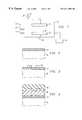
- FIGS. 2-4are simplified, cross-sectional views showing the steps employed in manufacturing a semiconductor device of the invention.
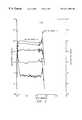
- FIGS. 5-6are graphs of the carbon, fluorine and nitrogen concentrations of SiO 2 films formed by conventional methods and formed with the tunable dielectric constants of the invention, respectively.
- FIG. 1shows a parallel plate type plasma CVD apparatus of the type which can be used in practicing the method of the invention.
- a gas within the chamber interior 13is discharged to the exterior thereof by means of a suitable pump 15 .
- Appropriately selected source gasesare introduced into the chamber interior 13 by means of a plurality of quartz nozzles 17 , 19 , 21 .
- a set of parallel plate electrodes 23 , 25are mounted within the chamber interior 13 .
- a variable frequency power source 27is connected to the top electrode 23 with the bottom electrode 25 being connected to a ground potential point 29 .
- a Si substrate 31is mounted on the lower electrode 25 .
- the dielectric constant of the oxide films produced according to the present methodcan be “tuned” by the selective addition of carbon, nitrogen or fluorine or all of the aforementioned to the oxide film.
- the process of the inventionallows the deposition of a conformal TEOS film which has been doped using carbon, nitrogen and fluorine. The process controls the percentage of carbon and fluorine that is added to the film in order to selectively “tune” the resulting dielectric constant of the film.
- the film doped only with carbon, fluorine and nitrogenhas shown improved transistor reliability performance over standard oxide films.
- One advantage of the present methodis that the starting gases can employ TEOS as the silicon source, thereby allowing conformal step coverage.
- the processcan be run using any plasma enhanced chemical vapor deposition (PECVD) deposition system, such as the radio frequency plasma assisted CVD system shown in FIG. 1 . Atmospheric or high density plasma systems may also be used to apply this film.
- PECVDplasma enhanced chemical vapor deposition
- the process of the inventionpreferably utilizes tetraethoxy silicate (TEOS) as the silicon source, although other silicon sources could be utilized besides TEOS.
- TEOStetraethoxy silicate
- Other silicon sourcesinclude, for example, HSi(N(CH 2 ) 2 ) 3 ; Si(N(CH 3 ) 2 ) 4 ; (CH 3 ) 3 SiN 3 ; and SiH 4 or mixtures thereof.
- the preferred oxidizing source gasesare N 2 O and O 2 although other sources of oxidizing gas could be utilized, as well, including NO, NH 3 , O 2 , or a combination of these gases.
- a preferred fluorine source gasis C 2 F 6 .
- Other fluorine source gaseswhich could be used include SiF 4 , CF 4 and mixtures thereof, or any other fluorine gaseous source conveniently available.
- N 2 Oalone or as one of the oxidizing source gases
- TEOSis not fully oxidized, leaving carbon behind in the film being produced.
- N 2 O and O 2within selected percentages with TEOS, different percentages of carbon can be left behind in the film.
- the percentage of fluorine and carbon added to the filmis controlled by the flow rate (partial pressure) of the C 2 F 6 gas source introduced to the process.
- the use of N 2 O as the oxidizing gas sourcealso leaves behind nitrogen in the film being produced.
- the addition of nitrogen to the filmchanges the doped silicon dioxide film to a doped oxynitride film.
- the oxynitride filmprovides a barrier to water and hydroxyl diffusion, thus allowing a more stable, lower dielectric constant film to be formed.
- Higher concentrations of fluorinecan be added to the oxynitride film above that of a standard fluorine doped silicon dioxide film to produce a final film with a lower dielectric constant.
- FIGS. 2-4illustrate, in simplified fashion, the steps of the method of the invention.
- a silicon oxide film containing fluorine, carbon and nitrogen having a given dielectric constantis formed by CVD method using a source gas containing at least silicon, nitrogen, oxygen, carbon and fluorine contributors.
- the Si substrate 31is mounted on the electrode 25 , followed by heating the substrate 31 to between 300° C.-500° C. with a resistance heater.
- a tetraethoxy silicate (TEOS) gas, N 2 O as an oxidizing source gas and C 2 F 6 as a fluorine source gasare simultaneously introduced into the chamber interior 13 at flow rates in the range of 4 to 10 L/min for C 2 F 6 , 5 to 12 L/min for N 2 O, 0.8 to 3 L/min for TEOS and 0.01 to 5 L/min for O 2 , respectively so as to set up a pressure of 10 microTorr to 1 atmosphere within the chamber.
- TEOStetraethoxy silicate
- Particularly preferred gas flow ratesare 6 L/min for C 2 F 6 , 10 L/min for N 2 O, 2.8 L/min for TEOS and 0.05 L/min for O 2 at a low relative pressure of about 2.6 Torr within the chamber interior 13 .
- the ratio of N 2 O to O 2 in the source gasescan be in the range of 1:1 to 1200:1 with a preferable setting of 200:1.
- the total RF power supplied to the electrode 23can be in the range of 0.1 to 2.5 KWatt with a preferred setting of 0.5 KWatts in order to cause a discharge and, thus, to form a doped oxynitride, SiO 2 like, film 33 (FIG. 2) on the Si substrate 35 .
- the ratio of the low frequency power, at 300 KHz, to high frequency power at 13.56 MHzwas in the range of 6:1 to 1:1 with a preferable setting of 1.5:1.
- an aluminum filmis formed by any convenient means, for example by physical vapor deposition followed by patterning the aluminum film to form a first aluminum wiring 37 (see FIG. 3 ).
- a SiO 2 film 39is formed in the same manner that the film 33 was formed.
- an aluminum filmis formed to cover the second SiO 2 film 39 followed by patterning the aluminum film to form a second aluminum wiring 41 , as in the formation of the first aluminum wiring 37 .
- a SiO 2 film 43is formed to cover the second aluminum wiring 41 .
- Conventional gap fill processessuch as SOG fill, can be used to locally planarize the space between adjacent metal lines. The use of the SOG local gap fill process will require the deposition of two doped oxynitride films to encapsulate the SOG film.
- a semiconductor devicein which a silicon oxide film acts as an insulating film for electrically isolating conductive layers included in the semiconductor device.
- the silicon oxide filmis formed containing fluorine, carbon and nitrogen and having a given dielectric constant value by the CVD method using a source gas which contains at least silicon, nitrogen, carbon, oxygen and fluorine contributors.
- a source gaswhich contains at least silicon, nitrogen, carbon, oxygen and fluorine contributors.
- the given dielectric constantis determined by controlling the relative ratios of N 2 O:O 2 :C 2 F 6 and TEOS as the source gases in the CVD method.
- the method of the inventionalso allows silicon oxide films to be produced which have increased dielectric constants to thereby provide a “tunable” dielectric constant oxide.
- a semiconductor deviceis manufactured in which a silicon oxide film is formed with regions having a relatively high dielectric constant. The regions of relatively high dielectric constant are used to form capacitors within the semiconductor device.
- a silicon oxide filmis formed containing metal oxides and having a given dielectric constant value by CVD method using a source gas which contains at least silicon, nitrogen and oxygen contributors which are introduced within a reaction chamber.
- a high dielectric compoundis also introduced into the reaction chamber which is preferably selected from the group consisting of either single source or mixtures of alkoxy compounds of the general formula MOR and/or titanate compounds of the general formula MTiO 3 and M 2 TiO 5 , where M is a alkali or alkaline earth metal, and/or ferroelectric materials to form a relatively high dielectric constant silicon oxide film.
- the high dielectric compoundcan be added to the reaction chamber by liquid or vapor injection into the CVD reaction chamber.
- the high dielectric compounds added to the reaction chamberhave a dielectric constant between about 15 and 12,000.
- Alkoxy (MOR) or titanate (MTiO 3 or M 2 TiO 5 ) compounds(where M is an alkali or alkaline earth metal, Ba, Sr, Ca, Mg) or ferroelectric compounds can be used in PECVD or CVD operations to form high dielectric constant oxide or ceramic films. Titanates in the pure form have dielectric constants between 15 to 12,000. The addition of these compounds to an oxynitride or silicon dioxide film will effectively form a composite film with an increased dielectric constant. The final film can be homogeneous, graded or layered.
- Oxoalkoxideshave been formed by thermal condensation of heteralkoxides, alkoxide, titanate or organic salts. The addition of these compounds either by liquid or vapor injection into a CVD or PECVD reactor would produce the desired increase in the dielectric constant of deposited film.
- an Si substrateis again mounted to an electrode, such as electrode 25 in FIG. 1, followed by heating the substrate 31 to between 100° C.-900° C., where 500° C. is the highest temperature possible for aluminum capacitor electrodes.
- a tetraethoxy silicate (TEOS) gas, N 2 O and O 2 as the oxidizing source gas, and titanium isopropoxideare simultaneously introduced into the chamber interior 13 at flow rates in the range of 0.8 to 2 L/min for TEOS, 0.01 to 12 L/min for N 2 O, 0.01 to 12 L/min for O 2 , and 0.01 to 10 L/min for titanium isopropoxide, receptively, so as to set up a pressure of 10 microTorr to 1 atmosphere within the chamber.
- TEOStetraethoxy silicate
- the ratio of N 2 O to O 2 in the source gasescan be in the range of 0.000008:1 to 1200:1 with a preferable setting of 0.3:1.
- the total RF power supplied to the electrode 23can be in the range of 0.1 to 2.5 KWatt with a preferred setting of 0.8 KWatts in order to cause a discharge and, thus, to form a high dielectric constant oxide film 33 (FIG. 2) on the Si substrate 35 .
- the ratio of the low frequency power, at 300 KHz, to high frequency power at 13.56 MHzwas in the range of 6:1 to 0.1:1 with a preferable setting of 1:1.
- the method of the inventionprovides a convenient means for tuning the dielectric constant of an oxide film of the type used in the manufacture of semiconductor devices.
- the dielectric constant of the oxide filmcan be lowered by doping the film with carbon or fluorine atoms. By lowering the dielectric constant of the oxide film below about 4.0, cross talk between adjacent conductive lines can be minimized.
- the method of the inventioncan employ a conventional TEOS as the silicon source gas which allows conformal step coverage. Also, the process can be run on any conventional CVD deposition system.
- two interconnect linescan be spaced in closer proximity, thereby lowering the operating voltage of the circuit.
- the use of a PECVD environmentis advantageous because of the relatively low temperatures required for metal interconnect lines.
- a convenient carbon and fluorine source gasis C 2 F 6 . Using this gas, it is possible to reduce the dielectric constant of the silicon oxide film from approximately 4.5 to about 3.5 or lower according to the teaching of the invention.
- the dielectric constant of the silicon oxide filmcan be raised to form capacitors within the semiconductor devices.
Landscapes
- Engineering & Computer Science (AREA)
- Physics & Mathematics (AREA)
- Condensed Matter Physics & Semiconductors (AREA)
- General Physics & Mathematics (AREA)
- Computer Hardware Design (AREA)
- Microelectronics & Electronic Packaging (AREA)
- Power Engineering (AREA)
- Manufacturing & Machinery (AREA)
- Formation Of Insulating Films (AREA)
- Internal Circuitry In Semiconductor Integrated Circuit Devices (AREA)
- Chemical Vapour Deposition (AREA)
Abstract
Description
Claims (3)
Priority Applications (4)
| Application Number | Priority Date | Filing Date | Title |
|---|---|---|---|
| US08/823,305US6211096B1 (en) | 1997-03-21 | 1997-03-21 | Tunable dielectric constant oxide and method of manufacture |
| PCT/US1998/005231WO1998043286A1 (en) | 1997-03-21 | 1998-03-16 | Tunable dielectric constant oxide and method of manufacture |
| AU64698/98AAU6469898A (en) | 1997-03-21 | 1998-03-16 | Tunable dielectric constant oxide and method of manufacture |
| TW087103907ATW432605B (en) | 1997-03-21 | 1998-03-17 | Tunable dielectric constant oxide and method of manufacture |
Applications Claiming Priority (1)
| Application Number | Priority Date | Filing Date | Title |
|---|---|---|---|
| US08/823,305US6211096B1 (en) | 1997-03-21 | 1997-03-21 | Tunable dielectric constant oxide and method of manufacture |
Publications (1)
| Publication Number | Publication Date |
|---|---|
| US6211096B1true US6211096B1 (en) | 2001-04-03 |
Family
ID=25238373
Family Applications (1)
| Application Number | Title | Priority Date | Filing Date |
|---|---|---|---|
| US08/823,305Expired - LifetimeUS6211096B1 (en) | 1997-03-21 | 1997-03-21 | Tunable dielectric constant oxide and method of manufacture |
Country Status (4)
| Country | Link |
|---|---|
| US (1) | US6211096B1 (en) |
| AU (1) | AU6469898A (en) |
| TW (1) | TW432605B (en) |
| WO (1) | WO1998043286A1 (en) |
Cited By (52)
| Publication number | Priority date | Publication date | Assignee | Title |
|---|---|---|---|---|
| US20010054733A1 (en)* | 1999-08-30 | 2001-12-27 | Vishnu Agarwal | Capacitors having a capacitor dielectric layer comprising a metal oxide having multiple different metals bonded with oxygen |
| US6365266B1 (en)* | 1999-12-07 | 2002-04-02 | Air Products And Chemicals, Inc. | Mesoporous films having reduced dielectric constants |
| US6426233B1 (en)* | 1999-08-03 | 2002-07-30 | Micron Technology, Inc. | Uniform emitter array for display devices, etch mask for the same, and methods for making the same |
| US20020167070A1 (en)* | 2000-06-30 | 2002-11-14 | Motorola, Inc. | Hybrid semiconductor structure and device |
| US6482754B1 (en)* | 2001-05-29 | 2002-11-19 | Intel Corporation | Method of forming a carbon doped oxide layer on a substrate |
| US6501121B1 (en)* | 2000-11-15 | 2002-12-31 | Motorola, Inc. | Semiconductor structure |
| US6555946B1 (en) | 2000-07-24 | 2003-04-29 | Motorola, Inc. | Acoustic wave device and process for forming the same |
| US20030104689A1 (en)* | 2001-12-05 | 2003-06-05 | Canon Sales Co., Inc. And Semiconductor Process Laboratory Co., Ltd. | Manufacturing method of semiconductor device |
| US6589856B2 (en) | 2001-08-06 | 2003-07-08 | Motorola, Inc. | Method and apparatus for controlling anti-phase domains in semiconductor structures and devices |
| US6590236B1 (en) | 2000-07-24 | 2003-07-08 | Motorola, Inc. | Semiconductor structure for use with high-frequency signals |
| US6592980B1 (en)* | 1999-12-07 | 2003-07-15 | Air Products And Chemicals, Inc. | Mesoporous films having reduced dielectric constants |
| US6627532B1 (en)* | 1998-02-11 | 2003-09-30 | Applied Materials, Inc. | Method of decreasing the K value in SiOC layer deposited by chemical vapor deposition |
| US6635529B2 (en)* | 2002-03-15 | 2003-10-21 | Oki Electric Industry Co., Ltd. | Method of fabricating semiconductor device |
| US6639249B2 (en) | 2001-08-06 | 2003-10-28 | Motorola, Inc. | Structure and method for fabrication for a solid-state lighting device |
| US6638838B1 (en) | 2000-10-02 | 2003-10-28 | Motorola, Inc. | Semiconductor structure including a partially annealed layer and method of forming the same |
| US20030207589A1 (en)* | 2002-05-03 | 2003-11-06 | Thoughtbeam, Inc. | Method for growing a monocrystalline oxide layer and for fabricating a semiconductor device on a monocrystalline substrate |
| US6646293B2 (en) | 2001-07-18 | 2003-11-11 | Motorola, Inc. | Structure for fabricating high electron mobility transistors utilizing the formation of complaint substrates |
| US6667196B2 (en) | 2001-07-25 | 2003-12-23 | Motorola, Inc. | Method for real-time monitoring and controlling perovskite oxide film growth and semiconductor structure formed using the method |
| US6673667B2 (en) | 2001-08-15 | 2004-01-06 | Motorola, Inc. | Method for manufacturing a substantially integral monolithic apparatus including a plurality of semiconductor materials |
| US6673646B2 (en) | 2001-02-28 | 2004-01-06 | Motorola, Inc. | Growth of compound semiconductor structures on patterned oxide films and process for fabricating same |
| US6677253B2 (en) | 2001-10-05 | 2004-01-13 | Intel Corporation | Carbon doped oxide deposition |
| US6693298B2 (en) | 2001-07-20 | 2004-02-17 | Motorola, Inc. | Structure and method for fabricating epitaxial semiconductor on insulator (SOI) structures and devices utilizing the formation of a compliant substrate for materials used to form same |
| US6693033B2 (en) | 2000-02-10 | 2004-02-17 | Motorola, Inc. | Method of removing an amorphous oxide from a monocrystalline surface |
| US6709989B2 (en) | 2001-06-21 | 2004-03-23 | Motorola, Inc. | Method for fabricating a semiconductor structure including a metal oxide interface with silicon |
| US20040095288A1 (en)* | 2002-11-14 | 2004-05-20 | The Penn State Research Foundation | Actively reconfigurable pixelized antenna systems |
| US6750141B2 (en) | 2001-03-28 | 2004-06-15 | Applied Materials Inc. | Silicon carbide cap layers for low dielectric constant silicon oxide layers |
| US20040185177A1 (en)* | 2001-07-13 | 2004-09-23 | Cem Basceri | Chemical vapor deposition methods of forming barium strontium titanate comprising dielectric layers, including such layers having a varied concentration of barium and strontium within the layer |
| US20040228968A1 (en)* | 2000-05-26 | 2004-11-18 | Micron Technology, Inc. | Chemical vapor deposition method for depositing a high k dielectric film |
| US6838122B2 (en) | 2001-07-13 | 2005-01-04 | Micron Technology, Inc. | Chemical vapor deposition methods of forming barium strontium titanate comprising dielectric layers |
| US6855992B2 (en) | 2001-07-24 | 2005-02-15 | Motorola Inc. | Structure and method for fabricating configurable transistor devices utilizing the formation of a compliant substrate for materials used to form the same |
| US6885065B2 (en) | 2002-11-20 | 2005-04-26 | Freescale Semiconductor, Inc. | Ferromagnetic semiconductor structure and method for forming the same |
| US6887780B2 (en) | 2001-08-31 | 2005-05-03 | Intel Corporation | Concentration graded carbon doped oxide |
| US6888188B2 (en) | 2001-08-17 | 2005-05-03 | Micron Technology, Inc. | Capacitor constructions comprising perovskite-type dielectric materials and having different degrees of crystallinity within the perovskite-type dielectric materials |
| US20050214457A1 (en)* | 2004-03-29 | 2005-09-29 | Applied Materials, Inc. | Deposition of low dielectric constant films by N2O addition |
| US6965128B2 (en) | 2003-02-03 | 2005-11-15 | Freescale Semiconductor, Inc. | Structure and method for fabricating semiconductor microresonator devices |
| US6992321B2 (en) | 2001-07-13 | 2006-01-31 | Motorola, Inc. | Structure and method for fabricating semiconductor structures and devices utilizing piezoelectric materials |
| US7005717B2 (en) | 2000-05-31 | 2006-02-28 | Freescale Semiconductor, Inc. | Semiconductor device and method |
| US7020374B2 (en) | 2003-02-03 | 2006-03-28 | Freescale Semiconductor, Inc. | Optical waveguide structure and method for fabricating the same |
| US7019332B2 (en) | 2001-07-20 | 2006-03-28 | Freescale Semiconductor, Inc. | Fabrication of a wavelength locker within a semiconductor structure |
| US7045815B2 (en) | 2001-04-02 | 2006-05-16 | Freescale Semiconductor, Inc. | Semiconductor structure exhibiting reduced leakage current and method of fabricating same |
| US7067856B2 (en) | 2000-02-10 | 2006-06-27 | Freescale Semiconductor, Inc. | Semiconductor structure, semiconductor device, communicating device, integrated circuit, and process for fabricating the same |
| US7105866B2 (en) | 2000-07-24 | 2006-09-12 | Freescale Semiconductor, Inc. | Heterojunction tunneling diodes and process for fabricating same |
| US7161227B2 (en) | 2001-08-14 | 2007-01-09 | Motorola, Inc. | Structure and method for fabricating semiconductor structures and devices for detecting an object |
| US7169619B2 (en) | 2002-11-19 | 2007-01-30 | Freescale Semiconductor, Inc. | Method for fabricating semiconductor structures on vicinal substrates using a low temperature, low pressure, alkaline earth metal-rich process |
| US7211852B2 (en) | 2001-01-19 | 2007-05-01 | Freescale Semiconductor, Inc. | Structure and method for fabricating GaN devices utilizing the formation of a compliant substrate |
| US7342276B2 (en) | 2001-10-17 | 2008-03-11 | Freescale Semiconductor, Inc. | Method and apparatus utilizing monocrystalline insulator |
| US20080179760A1 (en)* | 2007-01-31 | 2008-07-31 | Infineon Technologies Ag | Method for producing a device and device |
| US20090102027A1 (en)* | 2007-10-18 | 2009-04-23 | Semiconductor Energy Laboratory Co., Ltd. | Method for manufacturing semiconductor device, semiconductor device, and electronic appliance |
| US20090175378A1 (en)* | 2008-01-08 | 2009-07-09 | Robert Bogdan Staszewski | System and Method for Impedance Mismatch Compensation in Digital Communications Systems |
| US20090321895A1 (en)* | 2006-06-16 | 2009-12-31 | Toray Engineering Co., Ltd | Silicon thin-film and method of forming silicon thin-film |
| US20150325427A1 (en)* | 2011-03-23 | 2015-11-12 | Hitachi Kokusai Electric Inc. | Method of manufacturing semiconductor device, substrate processing method and substrate processing apparatus |
| US20190088545A1 (en)* | 2017-09-21 | 2019-03-21 | Toshiba Memory Corporation | Manufacturing method of semiconductor device |
Families Citing this family (2)
| Publication number | Priority date | Publication date | Assignee | Title |
|---|---|---|---|---|
| JP2000332010A (en) | 1999-03-17 | 2000-11-30 | Canon Sales Co Inc | Method of forming interlayer insulating film and semiconductor device |
| GB2373372B (en)* | 1999-11-30 | 2004-04-28 | Intel Corp | Improved flourine doped sio2 film |
Citations (16)
| Publication number | Priority date | Publication date | Assignee | Title |
|---|---|---|---|---|
| JPS6235562A (en)* | 1985-08-08 | 1987-02-16 | Nec Corp | Semiconductor device |
| US5145711A (en) | 1987-08-10 | 1992-09-08 | Semiconductor Energy Laboratory Co., Ltd. | Cyclotron resonance chemical vapor deposition method of forming a halogen-containing diamond on a substrate |
| US5198263A (en) | 1991-03-15 | 1993-03-30 | The United States Of America As Represented By The United States Department Of Energy | High rate chemical vapor deposition of carbon films using fluorinated gases |
| US5260134A (en) | 1991-02-14 | 1993-11-09 | Semiconductor Energy Laboratory Co., Ltd. | Organic composite |
| US5275850A (en) | 1988-04-20 | 1994-01-04 | Hitachi, Ltd. | Process for producing a magnetic disk having a metal containing hard carbon coating by plasma chemical vapor deposition under a negative self bias |
| US5288518A (en)* | 1991-06-07 | 1994-02-22 | Nec Corproation | Chemical vapor deposition method for forming fluorine containing silicon oxide film |
| JPH0677145A (en) | 1992-08-27 | 1994-03-18 | Toshiba Corp | Thin film formation method |
| US5296258A (en) | 1992-09-30 | 1994-03-22 | Northern Telecom Limited | Method of forming silicon carbide |
| US5324690A (en) | 1993-02-01 | 1994-06-28 | Motorola Inc. | Semiconductor device having a ternary boron nitride film and a method for forming the same |
| US5380557A (en) | 1991-08-29 | 1995-01-10 | General Electric Company | Carbon fluoride compositions |
| US5380516A (en) | 1988-05-28 | 1995-01-10 | Sumitomo Electric Industries, Ltd. | Process for synthesizing diamond in a vapor phase |
| US5413967A (en) | 1991-05-16 | 1995-05-09 | Kabushiki Kaisha Toshiba | Method of manufacturing semiconductor devices |
| US5423945A (en) | 1992-09-08 | 1995-06-13 | Applied Materials, Inc. | Selectivity for etching an oxide over a nitride |
| US5429995A (en) | 1992-07-17 | 1995-07-04 | Kabushiki Kaisha Toshiba | Method of manufacturing silicon oxide film containing fluorine |
| JPH08213386A (en) | 1995-02-08 | 1996-08-20 | Fujitsu Ltd | Method for manufacturing semiconductor device |
| US5618761A (en)* | 1994-09-16 | 1997-04-08 | Kabushiki Kaisha Toshiba | Method of manufacturing a perovskite thin film dielectric |
Family Cites Families (1)
| Publication number | Priority date | Publication date | Assignee | Title |
|---|---|---|---|---|
| US5470398A (en)* | 1990-09-25 | 1995-11-28 | Matsushita Electric Industrial Co., Ltd. | Dielectric thin film and method of manufacturing same |
- 1997
- 1997-03-21USUS08/823,305patent/US6211096B1/ennot_activeExpired - Lifetime
- 1998
- 1998-03-16AUAU64698/98Apatent/AU6469898A/ennot_activeAbandoned
- 1998-03-16WOPCT/US1998/005231patent/WO1998043286A1/enactiveApplication Filing
- 1998-03-17TWTW087103907Apatent/TW432605B/ennot_activeIP Right Cessation
Patent Citations (16)
| Publication number | Priority date | Publication date | Assignee | Title |
|---|---|---|---|---|
| JPS6235562A (en)* | 1985-08-08 | 1987-02-16 | Nec Corp | Semiconductor device |
| US5145711A (en) | 1987-08-10 | 1992-09-08 | Semiconductor Energy Laboratory Co., Ltd. | Cyclotron resonance chemical vapor deposition method of forming a halogen-containing diamond on a substrate |
| US5275850A (en) | 1988-04-20 | 1994-01-04 | Hitachi, Ltd. | Process for producing a magnetic disk having a metal containing hard carbon coating by plasma chemical vapor deposition under a negative self bias |
| US5380516A (en) | 1988-05-28 | 1995-01-10 | Sumitomo Electric Industries, Ltd. | Process for synthesizing diamond in a vapor phase |
| US5260134A (en) | 1991-02-14 | 1993-11-09 | Semiconductor Energy Laboratory Co., Ltd. | Organic composite |
| US5198263A (en) | 1991-03-15 | 1993-03-30 | The United States Of America As Represented By The United States Department Of Energy | High rate chemical vapor deposition of carbon films using fluorinated gases |
| US5413967A (en) | 1991-05-16 | 1995-05-09 | Kabushiki Kaisha Toshiba | Method of manufacturing semiconductor devices |
| US5288518A (en)* | 1991-06-07 | 1994-02-22 | Nec Corproation | Chemical vapor deposition method for forming fluorine containing silicon oxide film |
| US5380557A (en) | 1991-08-29 | 1995-01-10 | General Electric Company | Carbon fluoride compositions |
| US5429995A (en) | 1992-07-17 | 1995-07-04 | Kabushiki Kaisha Toshiba | Method of manufacturing silicon oxide film containing fluorine |
| JPH0677145A (en) | 1992-08-27 | 1994-03-18 | Toshiba Corp | Thin film formation method |
| US5423945A (en) | 1992-09-08 | 1995-06-13 | Applied Materials, Inc. | Selectivity for etching an oxide over a nitride |
| US5296258A (en) | 1992-09-30 | 1994-03-22 | Northern Telecom Limited | Method of forming silicon carbide |
| US5324690A (en) | 1993-02-01 | 1994-06-28 | Motorola Inc. | Semiconductor device having a ternary boron nitride film and a method for forming the same |
| US5618761A (en)* | 1994-09-16 | 1997-04-08 | Kabushiki Kaisha Toshiba | Method of manufacturing a perovskite thin film dielectric |
| JPH08213386A (en) | 1995-02-08 | 1996-08-20 | Fujitsu Ltd | Method for manufacturing semiconductor device |
Cited By (93)
| Publication number | Priority date | Publication date | Assignee | Title |
|---|---|---|---|---|
| US20040166665A1 (en)* | 1998-02-11 | 2004-08-26 | Applied Materials, Inc. | Method of decreasing the K value in SIOC layer deposited by chemical vapor deposition |
| US20040029400A1 (en)* | 1998-02-11 | 2004-02-12 | Applied Materials, Inc. | Method of decreasing the K value in SIOC layer deposited by chemical vapor deposition |
| US6627532B1 (en)* | 1998-02-11 | 2003-09-30 | Applied Materials, Inc. | Method of decreasing the K value in SiOC layer deposited by chemical vapor deposition |
| US7271528B2 (en) | 1999-08-03 | 2007-09-18 | Micron Technology, Inc. | Uniform emitter array for display devices |
| US6890446B2 (en) | 1999-08-03 | 2005-05-10 | Micron Technology, Inc. | Uniform emitter array for display devices, etch mask for the same, and methods for making the same |
| US6426233B1 (en)* | 1999-08-03 | 2002-07-30 | Micron Technology, Inc. | Uniform emitter array for display devices, etch mask for the same, and methods for making the same |
| US6824698B2 (en) | 1999-08-03 | 2004-11-30 | Micron Technology, Inc. | Uniform emitter array for display devices, etch mask for the same, and methods for making the same |
| US20040094505A1 (en)* | 1999-08-03 | 2004-05-20 | Knappenberger Eric J. | Uniform emitter array for display devices, etch mask for the same, and methods for making the same |
| US20010054733A1 (en)* | 1999-08-30 | 2001-12-27 | Vishnu Agarwal | Capacitors having a capacitor dielectric layer comprising a metal oxide having multiple different metals bonded with oxygen |
| US20060006450A1 (en)* | 1999-08-30 | 2006-01-12 | Al-Shareef Husam N | Capacitors having a capacitor dielectric layer comprising a metal oxide having multiple different metals bonded with oxygen |
| US6943392B2 (en) | 1999-08-30 | 2005-09-13 | Micron Technology, Inc. | Capacitors having a capacitor dielectric layer comprising a metal oxide having multiple different metals bonded with oxygen |
| US20070001206A1 (en)* | 1999-08-30 | 2007-01-04 | Agarwal Vishnu K | Capacitors having a capacitor dielectric layer comprising a metal oxide having multiple different metals bonded with oxygen |
| US20020102396A1 (en)* | 1999-12-07 | 2002-08-01 | Macdougall James Edward | Mesoporous films having reduced dielectric constants |
| US6818289B2 (en) | 1999-12-07 | 2004-11-16 | Air Products And Chemicals, Inc. | Mesoporous films having reduced dielectric constants |
| US6592980B1 (en)* | 1999-12-07 | 2003-07-15 | Air Products And Chemicals, Inc. | Mesoporous films having reduced dielectric constants |
| US20030157311A1 (en)* | 1999-12-07 | 2003-08-21 | Macdougall James Edward | Mesoporous films having reduced dielectric constants |
| US6942918B2 (en) | 1999-12-07 | 2005-09-13 | Air Products And Chemicals, Inc. | Mesoporous films having reduced dielectric constants |
| US6365266B1 (en)* | 1999-12-07 | 2002-04-02 | Air Products And Chemicals, Inc. | Mesoporous films having reduced dielectric constants |
| US6693033B2 (en) | 2000-02-10 | 2004-02-17 | Motorola, Inc. | Method of removing an amorphous oxide from a monocrystalline surface |
| US7067856B2 (en) | 2000-02-10 | 2006-06-27 | Freescale Semiconductor, Inc. | Semiconductor structure, semiconductor device, communicating device, integrated circuit, and process for fabricating the same |
| US7217617B2 (en) | 2000-05-26 | 2007-05-15 | Micron Technology, Inc. | Methods of forming a capacitor |
| US20050208219A1 (en)* | 2000-05-26 | 2005-09-22 | Cem Basceri | Method of forming a capacitor |
| US20050186688A1 (en)* | 2000-05-26 | 2005-08-25 | Cem Basceri | Chemical vapor deposition methods and physical vapor deposition methods |
| US6884475B2 (en) | 2000-05-26 | 2005-04-26 | Micron Technology, Inc. | Chemical vapor deposition method for depositing a high k dielectric film |
| US7052584B2 (en) | 2000-05-26 | 2006-05-30 | Micron Technology, Inc. | Method of forming a capacitor |
| US20040228968A1 (en)* | 2000-05-26 | 2004-11-18 | Micron Technology, Inc. | Chemical vapor deposition method for depositing a high k dielectric film |
| US7005717B2 (en) | 2000-05-31 | 2006-02-28 | Freescale Semiconductor, Inc. | Semiconductor device and method |
| US20020167070A1 (en)* | 2000-06-30 | 2002-11-14 | Motorola, Inc. | Hybrid semiconductor structure and device |
| US7105866B2 (en) | 2000-07-24 | 2006-09-12 | Freescale Semiconductor, Inc. | Heterojunction tunneling diodes and process for fabricating same |
| US6555946B1 (en) | 2000-07-24 | 2003-04-29 | Motorola, Inc. | Acoustic wave device and process for forming the same |
| US6590236B1 (en) | 2000-07-24 | 2003-07-08 | Motorola, Inc. | Semiconductor structure for use with high-frequency signals |
| US6638838B1 (en) | 2000-10-02 | 2003-10-28 | Motorola, Inc. | Semiconductor structure including a partially annealed layer and method of forming the same |
| US6501121B1 (en)* | 2000-11-15 | 2002-12-31 | Motorola, Inc. | Semiconductor structure |
| US7211852B2 (en) | 2001-01-19 | 2007-05-01 | Freescale Semiconductor, Inc. | Structure and method for fabricating GaN devices utilizing the formation of a compliant substrate |
| US6673646B2 (en) | 2001-02-28 | 2004-01-06 | Motorola, Inc. | Growth of compound semiconductor structures on patterned oxide films and process for fabricating same |
| US6750141B2 (en) | 2001-03-28 | 2004-06-15 | Applied Materials Inc. | Silicon carbide cap layers for low dielectric constant silicon oxide layers |
| US7045815B2 (en) | 2001-04-02 | 2006-05-16 | Freescale Semiconductor, Inc. | Semiconductor structure exhibiting reduced leakage current and method of fabricating same |
| US6482754B1 (en)* | 2001-05-29 | 2002-11-19 | Intel Corporation | Method of forming a carbon doped oxide layer on a substrate |
| US6709989B2 (en) | 2001-06-21 | 2004-03-23 | Motorola, Inc. | Method for fabricating a semiconductor structure including a metal oxide interface with silicon |
| US6992321B2 (en) | 2001-07-13 | 2006-01-31 | Motorola, Inc. | Structure and method for fabricating semiconductor structures and devices utilizing piezoelectric materials |
| US6838122B2 (en) | 2001-07-13 | 2005-01-04 | Micron Technology, Inc. | Chemical vapor deposition methods of forming barium strontium titanate comprising dielectric layers |
| US6982103B2 (en) | 2001-07-13 | 2006-01-03 | Micron Technology, Inc. | Chemical vapor deposition methods of forming barium strontium titanate comprising dielectric layers, including such layers having a varied concentration of barium and strontium within the layer |
| US20040241322A1 (en)* | 2001-07-13 | 2004-12-02 | Micron Technology, Inc. | Chemical vapor deposition methods of forming barium strontium titanate comprising dielectric layers, including such layers having a varied concentration of barium and strontium within the layer |
| US20040185177A1 (en)* | 2001-07-13 | 2004-09-23 | Cem Basceri | Chemical vapor deposition methods of forming barium strontium titanate comprising dielectric layers, including such layers having a varied concentration of barium and strontium within the layer |
| US7488514B2 (en) | 2001-07-13 | 2009-02-10 | Micron Technology, Inc. | Methods of forming barium strontium titanate layers |
| US7208198B2 (en) | 2001-07-13 | 2007-04-24 | Micron Technology, Inc. | Chemical vapor deposition methods of forming barium strontium titanate comprising dielectric layers, including such layers having a varied concentration of barium and strontium within the layer |
| US20050133127A1 (en)* | 2001-07-13 | 2005-06-23 | Cem Basceri | Methods of forming barium strontium titanate layers |
| US6646293B2 (en) | 2001-07-18 | 2003-11-11 | Motorola, Inc. | Structure for fabricating high electron mobility transistors utilizing the formation of complaint substrates |
| US6693298B2 (en) | 2001-07-20 | 2004-02-17 | Motorola, Inc. | Structure and method for fabricating epitaxial semiconductor on insulator (SOI) structures and devices utilizing the formation of a compliant substrate for materials used to form same |
| US7019332B2 (en) | 2001-07-20 | 2006-03-28 | Freescale Semiconductor, Inc. | Fabrication of a wavelength locker within a semiconductor structure |
| US6855992B2 (en) | 2001-07-24 | 2005-02-15 | Motorola Inc. | Structure and method for fabricating configurable transistor devices utilizing the formation of a compliant substrate for materials used to form the same |
| US6667196B2 (en) | 2001-07-25 | 2003-12-23 | Motorola, Inc. | Method for real-time monitoring and controlling perovskite oxide film growth and semiconductor structure formed using the method |
| US6589856B2 (en) | 2001-08-06 | 2003-07-08 | Motorola, Inc. | Method and apparatus for controlling anti-phase domains in semiconductor structures and devices |
| US6639249B2 (en) | 2001-08-06 | 2003-10-28 | Motorola, Inc. | Structure and method for fabrication for a solid-state lighting device |
| US7161227B2 (en) | 2001-08-14 | 2007-01-09 | Motorola, Inc. | Structure and method for fabricating semiconductor structures and devices for detecting an object |
| US6673667B2 (en) | 2001-08-15 | 2004-01-06 | Motorola, Inc. | Method for manufacturing a substantially integral monolithic apparatus including a plurality of semiconductor materials |
| US7309889B2 (en) | 2001-08-17 | 2007-12-18 | Micron Technology, Inc. | Constructions comprising perovskite-type dielectric |
| US20060246675A1 (en)* | 2001-08-17 | 2006-11-02 | Cem Basceri | Methods of forming capacitor constructions comprising perovskite-type dielectric materials |
| US20050191766A1 (en)* | 2001-08-17 | 2005-09-01 | Cem Basceri | Constructions comprising perovskite-type dielectric |
| US7011978B2 (en) | 2001-08-17 | 2006-03-14 | Micron Technology, Inc. | Methods of forming capacitor constructions comprising perovskite-type dielectric materials with different amount of crystallinity regions |
| US6888188B2 (en) | 2001-08-17 | 2005-05-03 | Micron Technology, Inc. | Capacitor constructions comprising perovskite-type dielectric materials and having different degrees of crystallinity within the perovskite-type dielectric materials |
| US6958267B2 (en) | 2001-08-17 | 2005-10-25 | Micron Technology, Inc. | Methods of forming perovskite-type dielectric materials with chemical vapor deposition |
| US6887780B2 (en) | 2001-08-31 | 2005-05-03 | Intel Corporation | Concentration graded carbon doped oxide |
| US20050161827A1 (en)* | 2001-08-31 | 2005-07-28 | Ebrahim Andideh | Concentration graded carbon doped oxide |
| US7091615B2 (en) | 2001-08-31 | 2006-08-15 | Intel Corporation | Concentration graded carbon doped oxide |
| US20040043555A1 (en)* | 2001-10-05 | 2004-03-04 | Ebrahim Andideh | Carbon doped oxide deposition |
| US6677253B2 (en) | 2001-10-05 | 2004-01-13 | Intel Corporation | Carbon doped oxide deposition |
| US7342276B2 (en) | 2001-10-17 | 2008-03-11 | Freescale Semiconductor, Inc. | Method and apparatus utilizing monocrystalline insulator |
| US20030104689A1 (en)* | 2001-12-05 | 2003-06-05 | Canon Sales Co., Inc. And Semiconductor Process Laboratory Co., Ltd. | Manufacturing method of semiconductor device |
| EP1321975A3 (en)* | 2001-12-05 | 2004-11-24 | Canon Sales Co., Inc. | Method for plasma depositing an insulating film with low dielectric constant for a semiconductor device |
| US6849959B2 (en) | 2002-03-15 | 2005-02-01 | Oki Electric Industry Co., Ltd. | Method of fabricating semiconductor device |
| US6635529B2 (en)* | 2002-03-15 | 2003-10-21 | Oki Electric Industry Co., Ltd. | Method of fabricating semiconductor device |
| US6916717B2 (en) | 2002-05-03 | 2005-07-12 | Motorola, Inc. | Method for growing a monocrystalline oxide layer and for fabricating a semiconductor device on a monocrystalline substrate |
| US20030207589A1 (en)* | 2002-05-03 | 2003-11-06 | Thoughtbeam, Inc. | Method for growing a monocrystalline oxide layer and for fabricating a semiconductor device on a monocrystalline substrate |
| US6885345B2 (en) | 2002-11-14 | 2005-04-26 | The Penn State Research Foundation | Actively reconfigurable pixelized antenna systems |
| US20040095288A1 (en)* | 2002-11-14 | 2004-05-20 | The Penn State Research Foundation | Actively reconfigurable pixelized antenna systems |
| US7169619B2 (en) | 2002-11-19 | 2007-01-30 | Freescale Semiconductor, Inc. | Method for fabricating semiconductor structures on vicinal substrates using a low temperature, low pressure, alkaline earth metal-rich process |
| US6885065B2 (en) | 2002-11-20 | 2005-04-26 | Freescale Semiconductor, Inc. | Ferromagnetic semiconductor structure and method for forming the same |
| US7020374B2 (en) | 2003-02-03 | 2006-03-28 | Freescale Semiconductor, Inc. | Optical waveguide structure and method for fabricating the same |
| US6965128B2 (en) | 2003-02-03 | 2005-11-15 | Freescale Semiconductor, Inc. | Structure and method for fabricating semiconductor microresonator devices |
| US20050214457A1 (en)* | 2004-03-29 | 2005-09-29 | Applied Materials, Inc. | Deposition of low dielectric constant films by N2O addition |
| US7776670B2 (en)* | 2006-06-16 | 2010-08-17 | Toray Engineering Co., Ltd. | Silicon thin-film and method of forming silicon thin-film |
| US20090321895A1 (en)* | 2006-06-16 | 2009-12-31 | Toray Engineering Co., Ltd | Silicon thin-film and method of forming silicon thin-film |
| US20080179760A1 (en)* | 2007-01-31 | 2008-07-31 | Infineon Technologies Ag | Method for producing a device and device |
| US7811860B2 (en)* | 2007-01-31 | 2010-10-12 | Infineon Technologies Ag | Method for producing a device and device |
| US20110175208A1 (en)* | 2007-10-18 | 2011-07-21 | Semiconductor Energy Laboratory Co., Ltd. | Method for manufacturing semiconductor device, semiconductor device, and electronic appliance |
| US20090102027A1 (en)* | 2007-10-18 | 2009-04-23 | Semiconductor Energy Laboratory Co., Ltd. | Method for manufacturing semiconductor device, semiconductor device, and electronic appliance |
| US7955994B2 (en)* | 2007-10-18 | 2011-06-07 | Semiconductor Energy Laboratory Co., Ltd. | Method for manufacturing semiconductor device, semiconductor device, and electronic appliance |
| US8278740B2 (en)* | 2007-10-18 | 2012-10-02 | Semiconductor Energy Laboratory Co., Ltd. | Method for manufacturing semiconductor device, semiconductor device, and electronic appliance |
| US20090175378A1 (en)* | 2008-01-08 | 2009-07-09 | Robert Bogdan Staszewski | System and Method for Impedance Mismatch Compensation in Digital Communications Systems |
| US20150325427A1 (en)* | 2011-03-23 | 2015-11-12 | Hitachi Kokusai Electric Inc. | Method of manufacturing semiconductor device, substrate processing method and substrate processing apparatus |
| US9761437B2 (en)* | 2011-03-23 | 2017-09-12 | Hitachi Kokusai Electric Inc. | Method of manufacturing semiconductor device, substrate processing method and substrate processing apparatus |
| US20190088545A1 (en)* | 2017-09-21 | 2019-03-21 | Toshiba Memory Corporation | Manufacturing method of semiconductor device |
Also Published As
| Publication number | Publication date |
|---|---|
| TW432605B (en) | 2001-05-01 |
| AU6469898A (en) | 1998-10-20 |
| WO1998043286A1 (en) | 1998-10-01 |
Similar Documents
| Publication | Publication Date | Title |
|---|---|---|
| US6211096B1 (en) | Tunable dielectric constant oxide and method of manufacture | |
| US6048766A (en) | Flash memory device having high permittivity stacked dielectric and fabrication thereof | |
| US6331494B1 (en) | Deposition of low dielectric constant thin film without use of an oxidizer | |
| US6355519B1 (en) | Method for fabricating capacitor of semiconductor device | |
| US20010006843A1 (en) | Method for forming a gate insulating film for semiconductor devices | |
| US6995069B2 (en) | Dielectric capacitor manufacturing method and semiconductor storage device manufacturing method | |
| US20070164437A1 (en) | Semiconductor device and method of manufacturing the same | |
| KR100494322B1 (en) | Method of manufacturing a capacitor in a semiconductor device | |
| KR20000027398A (en) | Method for forming perovskite nuclei of ferroelectric layer | |
| US20040011279A1 (en) | Method of manufacturing semiconductor device | |
| KR20030004082A (en) | Diffusion Prevention Film, Fabrication Method Therefor, Semiconductor Storage Device and Fabricating Method Therefor | |
| US6376391B1 (en) | Pulsed or tailored bias for filling gaps with low dielectric constant material | |
| KR20040057623A (en) | method for fabricating capacitor | |
| KR20010059285A (en) | Manufacturing method for capacitor of semiconductor device | |
| US7217614B2 (en) | Methods to form electronic devices and methods to form a material over a semiconductive substrate | |
| US6812510B2 (en) | Ferroelectric capacitor, process for manufacturing thereof and ferroelectric memory | |
| KR20010008527A (en) | Forming method of capacitor with TaON thin film | |
| JP4391240B2 (en) | Thin film forming method and semiconductor device | |
| KR100395507B1 (en) | Semiconductor device and the method of fabricating same | |
| JPH06163523A (en) | Method for manufacturing semiconductor device | |
| KR100618683B1 (en) | Capacitor Manufacturing Method of Semiconductor Memory Device | |
| JP2003017687A (en) | Semiconductor device | |
| KR20000076611A (en) | Silicon nitride composite hdp/cvd process | |
| KR100399903B1 (en) | Interlayer planarization method of semiconductor device | |
| KR100318456B1 (en) | A method for forming tantalum oxide capacitor in semiconductor device |
Legal Events
| Date | Code | Title | Description |
|---|---|---|---|
| AS | Assignment | Owner name:SYMBIOS LOGIC INC., COLORADO Free format text:ASSIGNMENT OF ASSIGNORS INTEREST;ASSIGNORS:ALLMAN, DERRYL D.J.;KWONG, DIM LEE;REEL/FRAME:008640/0060;SIGNING DATES FROM 19970207 TO 19970319 | |
| AS | Assignment | Owner name:SYMBIOS, INC ., COLORADO Free format text:CHANGE OF NAME;ASSIGNOR:SYMBIOS LOGIC INC.;REEL/FRAME:009089/0936 Effective date:19971210 | |
| AS | Assignment | Owner name:LSI LOGIC CORPORATION, CALIFORNIA Free format text:ASSIGNMENT OF ASSIGNORS INTEREST;ASSIGNOR:SYMBIOS, INC.;REEL/FRAME:009500/0554 Effective date:19980922 | |
| STCF | Information on status: patent grant | Free format text:PATENTED CASE | |
| FPAY | Fee payment | Year of fee payment:4 | |
| FEPP | Fee payment procedure | Free format text:PAYOR NUMBER ASSIGNED (ORIGINAL EVENT CODE: ASPN); ENTITY STATUS OF PATENT OWNER: LARGE ENTITY Free format text:PAYER NUMBER DE-ASSIGNED (ORIGINAL EVENT CODE: RMPN); ENTITY STATUS OF PATENT OWNER: LARGE ENTITY | |
| FPAY | Fee payment | Year of fee payment:8 | |
| FPAY | Fee payment | Year of fee payment:12 | |
| AS | Assignment | Owner name:DEUTSCHE BANK AG NEW YORK BRANCH, AS COLLATERAL AG Free format text:PATENT SECURITY AGREEMENT;ASSIGNORS:LSI CORPORATION;AGERE SYSTEMS LLC;REEL/FRAME:032856/0031 Effective date:20140506 | |
| AS | Assignment | Owner name:LSI CORPORATION, CALIFORNIA Free format text:CHANGE OF NAME;ASSIGNOR:LSI LOGIC CORPORATION;REEL/FRAME:033102/0270 Effective date:20070406 | |
| AS | Assignment | Owner name:AVAGO TECHNOLOGIES GENERAL IP (SINGAPORE) PTE. LTD Free format text:ASSIGNMENT OF ASSIGNORS INTEREST;ASSIGNOR:LSI CORPORATION;REEL/FRAME:035390/0388 Effective date:20140814 | |
| AS | Assignment | Owner name:LSI CORPORATION, CALIFORNIA Free format text:TERMINATION AND RELEASE OF SECURITY INTEREST IN PATENT RIGHTS (RELEASES RF 032856-0031);ASSIGNOR:DEUTSCHE BANK AG NEW YORK BRANCH, AS COLLATERAL AGENT;REEL/FRAME:037684/0039 Effective date:20160201 Owner name:AGERE SYSTEMS LLC, PENNSYLVANIA Free format text:TERMINATION AND RELEASE OF SECURITY INTEREST IN PATENT RIGHTS (RELEASES RF 032856-0031);ASSIGNOR:DEUTSCHE BANK AG NEW YORK BRANCH, AS COLLATERAL AGENT;REEL/FRAME:037684/0039 Effective date:20160201 | |
| AS | Assignment | Owner name:BANK OF AMERICA, N.A., AS COLLATERAL AGENT, NORTH CAROLINA Free format text:PATENT SECURITY AGREEMENT;ASSIGNOR:AVAGO TECHNOLOGIES GENERAL IP (SINGAPORE) PTE. LTD.;REEL/FRAME:037808/0001 Effective date:20160201 Owner name:BANK OF AMERICA, N.A., AS COLLATERAL AGENT, NORTH Free format text:PATENT SECURITY AGREEMENT;ASSIGNOR:AVAGO TECHNOLOGIES GENERAL IP (SINGAPORE) PTE. LTD.;REEL/FRAME:037808/0001 Effective date:20160201 | |
| AS | Assignment | Owner name:AVAGO TECHNOLOGIES GENERAL IP (SINGAPORE) PTE. LTD., SINGAPORE Free format text:TERMINATION AND RELEASE OF SECURITY INTEREST IN PATENTS;ASSIGNOR:BANK OF AMERICA, N.A., AS COLLATERAL AGENT;REEL/FRAME:041710/0001 Effective date:20170119 Owner name:AVAGO TECHNOLOGIES GENERAL IP (SINGAPORE) PTE. LTD Free format text:TERMINATION AND RELEASE OF SECURITY INTEREST IN PATENTS;ASSIGNOR:BANK OF AMERICA, N.A., AS COLLATERAL AGENT;REEL/FRAME:041710/0001 Effective date:20170119 | |
| AS | Assignment | Owner name:BELL SEMICONDUCTOR, LLC, ILLINOIS Free format text:ASSIGNMENT OF ASSIGNORS INTEREST;ASSIGNORS:AVAGO TECHNOLOGIES GENERAL IP (SINGAPORE) PTE. LTD.;BROADCOM CORPORATION;REEL/FRAME:044886/0001 Effective date:20171208 | |
| AS | Assignment | Owner name:CORTLAND CAPITAL MARKET SERVICES LLC, AS COLLATERA Free format text:SECURITY INTEREST;ASSIGNORS:HILCO PATENT ACQUISITION 56, LLC;BELL SEMICONDUCTOR, LLC;BELL NORTHERN RESEARCH, LLC;REEL/FRAME:045216/0020 Effective date:20180124 | |
| AS | Assignment | Owner name:BELL NORTHERN RESEARCH, LLC, ILLINOIS Free format text:SECURITY INTEREST;ASSIGNOR:CORTLAND CAPITAL MARKET SERVICES LLC;REEL/FRAME:060885/0001 Effective date:20220401 Owner name:BELL SEMICONDUCTOR, LLC, ILLINOIS Free format text:SECURITY INTEREST;ASSIGNOR:CORTLAND CAPITAL MARKET SERVICES LLC;REEL/FRAME:060885/0001 Effective date:20220401 Owner name:HILCO PATENT ACQUISITION 56, LLC, ILLINOIS Free format text:SECURITY INTEREST;ASSIGNOR:CORTLAND CAPITAL MARKET SERVICES LLC;REEL/FRAME:060885/0001 Effective date:20220401 |