US6208783B1 - Optical filtering device - Google Patents
Optical filtering deviceDownload PDFInfo
- Publication number
- US6208783B1 US6208783B1US09/280,413US28041399AUS6208783B1US 6208783 B1US6208783 B1US 6208783B1US 28041399 AUS28041399 AUS 28041399AUS 6208783 B1US6208783 B1US 6208783B1
- Authority
- US
- United States
- Prior art keywords
- waveguide section
- waveguide
- section
- optical filter
- filter
- Prior art date
- Legal status (The legal status is an assumption and is not a legal conclusion. Google has not performed a legal analysis and makes no representation as to the accuracy of the status listed.)
- Expired - Lifetime
Links
Images


Classifications
- G—PHYSICS
- G02—OPTICS
- G02B—OPTICAL ELEMENTS, SYSTEMS OR APPARATUS
- G02B6/00—Light guides; Structural details of arrangements comprising light guides and other optical elements, e.g. couplings
- G02B6/24—Coupling light guides
- G02B6/26—Optical coupling means
- G02B6/28—Optical coupling means having data bus means, i.e. plural waveguides interconnected and providing an inherently bidirectional system by mixing and splitting signals
- G02B6/293—Optical coupling means having data bus means, i.e. plural waveguides interconnected and providing an inherently bidirectional system by mixing and splitting signals with wavelength selective means
- G02B6/29346—Optical coupling means having data bus means, i.e. plural waveguides interconnected and providing an inherently bidirectional system by mixing and splitting signals with wavelength selective means operating by wave or beam interference
- G02B6/29361—Interference filters, e.g. multilayer coatings, thin film filters, dichroic splitters or mirrors based on multilayers, WDM filters
- G02B6/29362—Serial cascade of filters or filtering operations, e.g. for a large number of channels
- G—PHYSICS
- G02—OPTICS
- G02B—OPTICAL ELEMENTS, SYSTEMS OR APPARATUS
- G02B6/00—Light guides; Structural details of arrangements comprising light guides and other optical elements, e.g. couplings
- G02B6/24—Coupling light guides
- G02B6/26—Optical coupling means
- G02B6/262—Optical details of coupling light into, or out of, or between fibre ends, e.g. special fibre end shapes or associated optical elements
- G—PHYSICS
- G02—OPTICS
- G02B—OPTICAL ELEMENTS, SYSTEMS OR APPARATUS
- G02B6/00—Light guides; Structural details of arrangements comprising light guides and other optical elements, e.g. couplings
- G02B6/02—Optical fibres with cladding with or without a coating
- G02B6/02052—Optical fibres with cladding with or without a coating comprising optical elements other than gratings, e.g. filters
Definitions
- This inventionrelates to the filtering of light propagating within waveguides, including optical fibers.
- waveguideis used herein to refer to an optical structure having the ability to transmit light in a bound propagation mode along a path parallel to its axis, and to contain the energy within or adjacent to its surface.
- filtersincluding interference filters, are commonly used for this filtering.
- the power density of light propagating within a waveguidemay be unacceptably high for the filter, having detrimental effects that may include damage to the filter material or reduced filter performance.
- filtersare typically employed by means of bulky, multiple-optical-element assemblies inserted between waveguides, which produces a variety of detrimental effects.
- Separate optical elementscan be difficult to align in an assembly and it can be difficult to maintain the alignment in operation as well. Each element often must be separately mounted with great precision and the alignment maintained.
- an increase in the number of pieces in an optical assemblytends to reduce the robustness of the assembly; the components may be jarred out of alignment or may break.
- interfaces between optical elementsoften result in significant signal losses and performance deterioration, especially when an air gap is present in the interfaces.
- the materials of which the additional elements are composedmay also introduce fluorescence or other undesirable optical interference into the assembly.
- filtering assembliesare often a problem as well. Not only can it be difficult to manufacture a filter on a small surface area, but also filtering assemblies usually contain bulky light-collimating, alignment and mounting components in addition to the filtering element. However, space is often at a premium in optical assemblies.
- interference filterschange depending upon the angle at which light is incident on the filter, and interference filters are generally designed for the filtration of normally incident light.
- FIG. 1for many purposes light can be envisioned as numerous light rays 101 simultaneously traveling down the length of a waveguide 102 at different angles.
- FIG. 1when an optical filter 103 is placed in the path of light 101 that is propagating within a waveguide 102 , much of the light 101 strikes the filter 103 at angles departing significantly from normal to the filter surface 103 , adversely affecting filter performance.
- angular orientationPrior to incidence of light upon an interference filter that is normal to the longitudinal axis of a waveguide, it is desirable to reduce the angle between the path of travel of light traveling within the waveguide and the longitudinal axis of the waveguide, referred to herein as the “angular orientation” of the light.
- Various meanshave been used for reducing the angular orientation of light traveling within a waveguide for the purpose of interaction with an interference filter, including the construction of elaborate optical assemblies (see U.S. Pat. No. 5,112,127 to Carrabba et al.), the insertion of “ball lenses” or “microlenses” (see U.S. Pat. No.
- FIG. 2depicts an optical assembly that includes three optical fibers, one of which has a filter 201 applied to its end face 202 .
- light 203 propagating in a first fiber 204crosses a junction between the optical fibers 205 before impinging upon the filter 201 applied to the end face 202 of the second optical fiber 206 .
- the gap 205 between the first optical fiber 204 and the second optical fiber 206because of the gap 205 between the first optical fiber 204 and the second optical fiber 206 , light having a significant orientation misses the second optical fiber 206 and is lost.
- optical architectures incorporating single mode optical fibersare associated with the small percentage of the fiber end face that is active. Not only is the optically active core extremely small, but a large radial distance separates the optically active core and surrounding region from the optical fiber end face's outer circumference. This characteristic of optical fibers, especially single mode optical fibers, makes alignment of optical fibers extremely difficult when a filter is interposed between them.
- the instant inventionsatisfies the foregoing needs.
- the inventionincludes an optical filter, a first section of waveguide and a second section of waveguide positioned between the first section of waveguide and the optical filter.
- the diameter of the second waveguide sectionis greater on the end proximate to the optical filter than on the end opposite the optical filter.
- the first waveguide section and second waveguide sectioncan either be separate optical components or can be fabricated as separate regions of the same waveguide.
- the shape of the second waveguide sectioncan vary depending upon manufacturing and performance considerations.
- the diameter of the second waveguidemay change at a constant taper, or the degree of the taper may vary over the length of the second waveguide section.
- the degree of taperis constant throughout the second waveguide section, which is relatively easy to manufacture.
- the second waveguide sectionis designed so that at each point over the length of the second waveguide section the slope of the taper varies so as to optimize the overall effect of the second waveguide section given manufacturing and design constraints.
- the section waveguide sectionhas a finite number of distinct longitudinal sections having varying angles of taper.
- a relatively lengthy second waveguide sectioncan be used to optimize the collimation of light for filtering.
- the second waveguide sectionmay be truncated or the shape of the second waveguide section designed so as to optimize collimation within the constraint of having a specified maximum length.
- Material of varying refractive indexcan be incorporated into the second waveguide section in order to achieve a number of effects that may be desirable, depending upon design considerations.
- the inventioncan further include a third waveguide section opposite the filter from the second waveguide section.
- the diameter of the third waveguide sectionwill also be greater on the end adjacent to the optical filter than on the end opposite the optical filter.
- the deviceis oriented so that light passes through the second waveguide section before reaching the filter.
- the paths of light rayswill be dispersed and collimated, reducing the power density of the light and at the same time reducing the average angular orientation of the light, thereby improving the performance of the filter assembly.
- the devicecan be oriented so that light propagates through it in the opposite direction and interacts with the filter before entering the second waveguide section.
- the second waveguide sectioncauses light with an unacceptably high angular orientation, which will have been improperly filtered by the filter, to be eliminated from the optical system by increasing its angular orientation beyond the propagation limits of either the second waveguide section or the first, waveguide section, and in addition concentrates the light into a smaller cross-sectional area, possibly for coupling into a first waveguide section having a cross-section smaller than the end of the second waveguide section to which it is coupled.
- the filtercan be placed at an oblique angle with respect to the longitudinal axis of the second waveguide section, which has a number of beneficial effects including reducing back-reflection of light.
- the filtercan be included in the device by a number of methods.
- the filtercan be coated onto the end surface of the second waveguide section, or it can be coated onto a substrate that is transparent to relevant wavelengths and the substrate mounted in optical communication with the second waveguide section.
- the second waveguide sectioncan further include opaque material behind the wall of the second waveguide section in order to reduce light leakage.
- the second waveguide sectioncan be constructed of any number of materials, including silica and low- to no-expansion glass such as ZERODUR® glass.
- FIG. 1is a cross-sectional view of an optical fiber having a filter adhering to its end face.
- FIG. 2depicts an optical assembly that includes three optical fibers, one of which has a filter applied to its end face.
- FIG. 3is a cross-sectional view of an embodiment of the invention in which the second waveguide has a constant taper.
- FIG. 4is a cross-sectional view of another embodiment of the invention in which the taper of the second waveguide section varies continuously.
- FIG. 5is a cross-sectional view of another embodiment of the invention in which the second waveguide section consists of three sections having varying angular orientations.
- FIG. 6is a cross-sectional illustration of light propagating through an embodiment of the invention having a constant taper through the second waveguide section.
- FIG. 7is a cross-sectional illustration of light propagating through an embodiment of the invention having a constant taper through the second waveguide section.
- FIG. 8is a cross-sectional illustration of light propagating through an embodiment of the invention in which the second waveguide section consists of two sections, one having an angular orientation of three degrees and one having an angular orientation of one degree.
- FIG. 9is a cross-sectional illustration of light propagating through an embodiment of the invention in which the portion of the second waveguide region that is closest to the end of the first waveguide region comprises material the refractive index of which increases as distance from the end of the first waveguide region increases.
- FIG. 10is a view of a meridional plane of an embodiment of the instant invention.
- FIG. 11is a cross-sectional view of an embodiment of the invention further including a third waveguide section located opposite the filter from the second waveguide section.
- FIG. 12is a cross-sectional view of an embodiment of the invention in which its orientation in the light path is reversed from the usual orientation.
- FIG. 13is a cross-sectional view of an embodiment of the invention in which the filter is mounted at an oblique angle with respect to the longitudinal axis of light propagation.
- FIG. 14is a cross-sectional view of two filters in series on the ends of a waveguide segment.
- FIG. 15is a perspective view of an embodiment of the present invention incorporated into an assembly so as to couple light from a single waveguide section into a bundle of waveguide sections.
- FIG. 16is a view of a wavelength division multiplexing device constructed in accordance with embodiment of the instant invention.
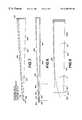
- FIG. 3illustrates an embodiment 300 a of the invention.
- the inventionincludes an optical filter 301 , a first waveguide section 302 and a second waveguide section 303 positioned between the filter 301 and the first waveguide section 302 .
- the diameter of the second waveguide section 303is greater on the end proximate to the optical filter 304 than on the end opposite the optical filter 305 .
- the first waveguide section 302 and the second waveguide section 303can either be separate optical components or can be fabricated as separate regions of the same waveguide.
- the light ray 306As a light ray 306 emerges from the first waveguide section 302 traveling at angle ⁇ with respect to the longitudinal axis 307 of the first waveguide section 302 , the light ray 306 enters the second waveguide section 303 of the device, which tapers at a constant angle ⁇ .
- the angle of incidence of the light ray 306 with respect to the wall of the second waveguide section 308will be ⁇ - ⁇ .
- the angle of reflection of the light ray 306 off of the wall of the second waveguide section 308will equal the angle of incidence of the light ray 306 onto the wall of the second waveguide section 308 , or ⁇ - ⁇ .
- the wall of the second waveguide section 308itself is oriented at angle ⁇ with respect to the longitudinal axis 307 of the waveguide sections, so after reflection by the wall of the second waveguide section 308 , the light ray 306 will therefore be traveling at an angle equal to ⁇ -2 ⁇ with respect to the longitudinal axis 307 . Therefore, the effect of a reflection of a light ray at the wall of the second waveguide section 308 will be to reduce the angular orientation of the light ray by 2 ⁇ .
- the reverse taper of the second waveguide sectionalso produces an expanding cross-sectional area in which the light propagates, resulting in reduced power density. These decreases in power density and average angular orientation of light striking the filter will result in improved filter performance.
- the device 300 ais coupled to another device or waveguide through a cross-sectional area approximately the same as the cross-sectional area of the filter end 307 of the second waveguide section 303 , and the optical axes of the devices are to be parallel, the alignment will be easier and for a given amount of alignment error the junction will have lower losses than if two cross-sectional areas the same as the cross-sectional area of the first waveguide section 302 were to be coupled together.
- This ready achievement of parallelism between elementscan be a very important characteristic for assemblies involving the filtering of light between two single mode optical fiber segments.
- the collimation of the light 306may result in lower losses.
- the shape of the second waveguide sectioncan vary depending upon manufacturing and performance considerations.
- the diameter of the second waveguide sectionmay change at a constant taper, as shown in FIG. 3 .
- This configurationhas the advantage of being readily manufactured.
- the angle of the tapercan vary over the length of the second waveguide section 303 as illustrated by the embodiment 300 b shown in FIG. 4 .
- the second waveguide section 303is designed so that at each point over the length of the second waveguide section 303 the slope of the taper varies so as to optimize the overall effect of the second waveguide section given manufacturing and design constraints.
- the second waveguide section 303has a finite number of distinct longitudinal sections having varying angles of taper as illustrated in FIG. 5 .
- the second waveguide sectionmay also have one or more non-tapered regions.
- the desired shape of the second waveguide sectionwill be determined by weighing considerations including cost of manufacture, the importance of optimal collimation of light in the particular application, design limitations such as the permitted or desired length of the assembly, and the geometries of the first waveguide section and of the interface between the first waveguide section and the second waveguide section.
- the second waveguide sectionmay have a constant taper as shown in FIG. 3 .
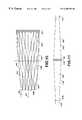
- the constant taper of the second waveguide section in this embodiment 300 acan be readily manufactured. However, as can be explained by reference to FIGS. 6, 7 and 8 , optimal collimation of light will be achieved when the taper of the wall of the second waveguide section decreases as distance from the first waveguide section increases and when the second waveguide section is relatively lengthy.
- FIG. 6is a representation of an embodiment 300 d of the instant invention in which the wall of the second waveguide section 308 has a constant taper.
- both a first light ray 602 having the maximum angular orientation that will be propagated by the first waveguide section and a second light ray 603 having a considerably lower angular orientationcan reach a point 605 within the second waveguide section 303 that is just beyond the end of the first waveguide section 607 .
- Point 608 in FIG. 6is the point at which a light ray with the maximum possible angular orientation 609 that is reflected at a point just at the end of the first waveguide section 607 will intersect the wall of the second waveguide section 308 in the second waveguide section 303 .
- FIG. 7is a representation of an embodiment 300 e of the instant invention in which the wall 308 of the second waveguide section 303 has a constant taper of three degrees.
- a light ray with an angular orientation of 8.5 degrees 703exits the first waveguide section 302 and is reflected by the wall 308 of the second waveguide section 303 at a point 705 just outside the first waveguide section 302 .
- the light ray 703will have an angular orientation of two and one half degrees. From that point the light ray 703 will travel unimpeded to the filter 301 and will impact the filter 301 at an angle two and one half degrees from normal.
- FIG. 8represents an embodiment 300 f of the instant invention in which the wall 308 of the second waveguide section 303 has a taper of three degrees up to a point 802 , but beyond that point 802 has an angular orientation of one degree.
- the same light ray with an angular orientation of 8.5 degrees 803exits the first waveguide section 302 and is reflected by the wall 308 of the second waveguide section 303 at the same point 805 just outside the first waveguide section 302 , and the same light ray with an angular orientation of two degrees 806 exits the first waveguide section 302 .
- the taper of the wall 308 of the second waveguide section 303decreases to less than that of the two light rays 803 and 806 , the light rays 803 and 806 and the wall 308 of the second waveguide section 303 converge rather than diverge.
- the first light ray 803is reflected by the wall 308 of the second waveguide section 303 a second time at point 807 , this time reducing the angular orientation of the light ray to one-half of one degree from two and one-half degrees, and the second light ray 806 now converges with the wall 308 of the second waveguide section 303 and is reflected at point 808 so as to reduce its angular orientation from two degrees to zero degrees.
- the average taper of the wall of the second waveguide sectionshould be lower at points distant from the end of the first waveguide section than at points proximate to the end of the first waveguide section.
- Those skilled in the artwill appreciate that in actually designing the shape of the second waveguide section, many factors will need to be taken into account. For example, as illustrated in FIG. 7, light with an angular orientation of less than ⁇ will not strike the wall of the second waveguide section 308 in the part of the second waveguide section 303 in which the wall 308 of the second waveguide section 303 has an angular orientation of ⁇ because the wall 308 of the second waveguide section 303 will diverge from the path of the light ray.
- the length of the second waveguide sectionwill depend upon manufacturing and design constraints. As described above and as illustrated by FIGS. 6, 7 and 8 , a lengthy second waveguide section can benefit performance, particularly if the shape of the second waveguide section is optimized throughout the second waveguide section. In addition, because of the tapered shape the cross-sectional area of the second waveguide section continues to increase as the second waveguide section is lengthened. This reduces the power density and may provide more room for error in alignment and coupling, as described elsewhere herein.
- the second waveguide sectioncan be truncated at a point at which the maximum or average angular orientation of light reaching the wall of the second waveguide section will not exceed a value that will be the threshold value for acceptable filter performance, or the shape of the second waveguide section designed so as to optimize collimation within the constraint of having a specified maximum length. This will result in a shorter or more compact configuration for the invention.
- FIG. 9illustrates an embodiment 300 g in which the portion 901 of the second waveguide section 303 that is closest to the end 607 of the first waveguide section 302 comprises material the refractive index of which increases as distance from the end 607 of the first waveguide section 302 increases.
- the angular orientation of light propagating within the second waveguide section 303is decreased prior to incidence upon the wall 308 of the second waveguide section 303 at point 905 .
- thisenables a design in which the angle of the taper of the wall 308 of the second waveguide section 303 is lower near the end 607 of the first waveguide section 302 and closer to the angular orientation found at points more distant from the end 607 of the first waveguide section 302 .
- Thiswill make the contour of the wall 308 of the second waveguide section 303 easier to manufacture. Because the relatively large angular orientation of the wall 308 of the second waveguide section 303 at points near the first waveguide section 302 is reduced, the second waveguide section 303 will have a slightly smaller cross-sectional area.
- FIG. 10is a view of a meridional plane of an embodiment 300 h of the instant invention.
- Each light ray 1001 propagating within the first waveguide section 302 and the second waveguide section 303can be analyzed as two separate, component rays.
- the first, meridional, componentpropagates parallel to the meridional plane represented by FIG. 10 .
- the second, nonmeridional, componentpropagates within a plane that is perpendicular to the meridional plane.
- One method of analysisis to ignore the nonmeridional component of every light ray 1001 propagating within the waveguide sections 302 and 303 , because it will bounce endlessly around the perimeter of the core of the first waveguide section 302 in a single plane that is perpendicular to the longitudinal axis 307 of the first and second waveguide sections 302 and 303 and will never exit the first waveguide section 302 . Therefore, for the purpose of optimizing the form of the instant invention, light exiting the first waveguide section 302 and entering the second waveguide section 303 can be analyzed by examining only a meridional plane.
- the analysisis done by means of a computer simulation, in two dimensions, of light 1001 propagating within the second waveguide section 303 .
- the boundary 1005 between the planar sections of the first waveguide section 302 and the second waveguide section 303is divided into multiple sub-segments: five sub-segments in the case of FIG. 10 .
- multiple rays 1001 having angular orientations ranging across the possible range of angular orientationsare projected from the center point of each sub-segment.
- three rays 1001are projected from the center point of each sub-segment.
- the wall 308 of the second waveguide section 303is broken into segments for analysis. For simplicity, in FIG.
- the wall 308 of the second waveguide section 303is analyzed as two segments: one segment proximate to the end face of the optical fiber 1006 and another segment 1007 that extends from the end of the first segment 1006 to the filter 301 .
- Computer simulationsare performed showing the results of the interaction of the multiple light rays 1001 with the segments 1006 and 1007 of the wall 308 of the second waveguide section 303 as the angles of the wall segments 1006 and 1007 are incrementally changed.
- 121 simulationsmight be performed: 11 simulations with the first segment 1006 having an angular orientation of five degrees and the second segment 1007 having angular orientations ranging from five to zero degrees in one-half degree increments, 11 simulations with the first segment 1006 having an angular orientation of four and one half degrees and the second segment 1007 having angular orientations ranging from five to zero degrees in one-half degree increments, and so on.
- the paths of the light rays 1001would be adjusted to reflect the presence of any variable refractive index material present in the second waveguide region 303 .
- This simulation method for designing the shape of the second waveguide sectioncan be utilized in three dimensions as well. Procedures for doing so will be evident to those skilled in the art.
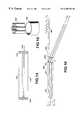
- the inventioncan further include a third waveguide section 1101 opposite the filter 301 from the second waveguide section 303 .
- the diameter of the third waveguide section 1101is greater on the end 1105 adjacent to the optical filter 301 than on the end opposite the optical filter 1106 .
- the third waveguide section 1101serves to concentrate and increase the angular orientation of light that has been filtered.
- One example of when this embodiment 300 i would be desirableis the filtering of light propagating within an optical fiber, which could be the first waveguide section 1107 .
- a third waveguide section 1101can reduce the cross section of the area within which the filtered signal propagates, enabling the entire signal to be coupled into a normally sized optical fiber region 1108 .
- the instant inventioncan also be used in a reversed position in which light first strikes the filter and then enters the second waveguide section.
- This embodiment 300 jis illustrated in FIG. 12 .
- light 1201 with an angular orientation significant enough to cause unacceptable error in filter 301 performancewill strike and pass through the filter 301 .
- Such light 1201will be filtered, but its spectral characteristics will deviate from the desired characteristics.
- This light 1201will have a relatively high angular orientation after passing through the filter 301 and entering the second waveguide section 303 .
- the taper of the wall 308 of the second waveguide section 303is a forward taper rather than a reverse taper and the effect is reversed: the mean angular orientation of light reflected by the surface increases.
- the inventionserves to cause improperly filtered light to be eliminated from a system after filtering.
- This configurationalso serves to reduce the cross-sectional area through which the filtered light propagates, which can be useful for coupling the light into other components such as a first waveguide section 302 having a cross-sectional area smaller than the cross-sectional area of the second waveguide section 303 to which it is coupled.
- the filter 301can be placed at an oblique angle ⁇ with respect to the longitudinal axis 307 of the second waveguide section 303 .
- light that is not passed by an interference filterwill be reflected by the filter.
- the back-reflected light 1304is rejected outside of the angular propagation limit of either the second waveguide section 303 or the first waveguide section 302 .
- the instant inventionoffers significant advantages over applying a filter directly to an angled fiber interface as taught in U.S. Pat. No. 5,037,180 to Stone.
- Back-reflected lightcan be detrimental, and eliminating or reducing back-reflected light may be of benefit in a number of ways.
- the interference light 1401can be trapped between filters 1402 and 1404 .
- the filtering schemeloses its effectiveness as some of the trapped light 1401 eventually passes through the second filter 1405 ; nonlinear effects also contribute to problems and corrupt the system performance.
- Second, back-reflected laser lightdue to normal filter inefficiencies, increases the light power intensity within the fiber. The additional power intensity generates additional fiber-photon interactions and may cause fiber interference and additional detrimental effects as well.
- lightmay also be intentionally reflected back-and-forth within a waveguide segment or similar bounded region for uses such as amplification of signals and creating constructive/destructive patterns of light interference for precise filtering.
- the instant inventionprovides improved control over patterns of intentionally reflected light within a fiber optic assembly.
- back-reflected laser lightcan interfere with a laser's stability if it is back-propagated into the laser. Eliminating or reducing back-reflected light may address these detrimental effects.
- lower-efficiency, less expensive filters, which inadvertently back-reflect a larger percentage of desired light,can be used if other steps are taken to counteract the corresponding increase in back-reflected light.
- the oblique angle of the filter 301provides a means to add or drop spectral regions of light propagating along an optical path.
- a first optical device 1310 having optical axis 307is positioned along the optical axis 307 of the second waveguide section 303 and in front of the filter 301 end face. Consequently, the first optical device 1310 is offset an angle ⁇ from the normal axis 1312 of the filter plane taken at the intersection of the filter 301 and the second waveguide section's axis 307 .
- a second optical device having optical axis 1313is also offset by an angle ⁇ from the normal axis 1312 but on the opposite side of the normal axis 1312 of the filter plane from the first optical device 1310 .
- the pathsare depicted as if the medium in the region 1314 between the devices has the same refractive index as that of the transmitting region of the second waveguide section 303 .
- thisis not a requirement and appropriate geometric and optical adjustments may be effected to compensate for deviations in refractive index.
- the first optical device 1310delivers multiple spectral regions of light, some spectral regions pass through the filter 301 and on into the second waveguide section 303 , other remaining spectral regions are reflected by the filter 301 and propagate toward the second optical device 1311 . Consequently, specific wavelength regions are dropped.
- the second optical device 1311may deliver light having minimal intensity within void spectral regions and having notable intensity within other, active spectral regions.
- the active spectral regionsreflect off the filter 301 and on toward the first optical device 1310 along with added light passing from the second waveguide section 303 through the filter 301 such that at least some portion of the spectral void is filled.
- the first 1310 and second 1311 optical devicesmay simply be waveguides or they may be collectively or individually passive or active elements.
- the assembly represented in FIG. 13may be a unit replicated repeatedly within an optical assembly or complex network.
- the manipulationcan preserve the modal patterns of the first waveguide section so that those patterns are extended further along the optical path outside the first waveguide section than would otherwise be possible.
- the manipulationcan deliberately convolve the modal patterns between the first waveguide section and the filter plane. Electromagnetic wave equations are readily applied to the analytical techniques and design methodology taught herein.
- the basic stepsare to form a second waveguide section in an appropriate shape, to provide for a filter at the end of the second waveguide section, to provide for a reflective surface at the wall of the second waveguide section and to couple the first and second waveguide sections.
- One method for forming the second waveguide sectionis to heat and stretch a cylindrical segment of optical material that has a diameter at least as great as the greatest diameter of the desired second waveguide section. During the pulling process, the temperature and tension are closely controlled. The profile may be monitored by laser interferometry or similar means.
- the cylindrical segmentcan be an optical fiber, and the process can be managed so that the cladding of the optical fiber remains intact, possibly negating the need to apply an additional coating to the wall of the second waveguide section.
- Another method for forming the second waveguide section in an appropriate shapeinvolves starting with a piece of silica or of an optical fiber that has a core diameter at least as great as the maximum desired diameter of the second waveguide section, and removing unwanted material in order to produce the desired shape by means of grinding or laser machining.
- Yet another method of manufactureis to heat an optical fiber segment to soften it and then to mold the heated optical fiber segment into the desired shape.
- a second waveguide sectioncould be manufactured by applying pressure squarely on the end of a heated optical fiber segment by means of a surface that is parallel to the end face of the optical fiber. Mass production of second waveguide sections can be achieved by placing multiple optical fiber segments into a tooling jig and simultaneously applying pressure squarely on the ends of all of the optical fiber segments.
- a different method for forming the second waveguide sectionis to drill or otherwise excavate an appropriately shaped crevice into the end of an optical fiber and to fill the crevice with a suitable material such as glass having a lower melting point than the glass of which the optical fiber is formed or a plastic melt.
- the second waveguide sectioncan be constructed of any number of materials, including silica and low- to no-expansion glass such as ZERODUR® glass.
- the filtercan be included in the device by a number of methods.
- the filtercan be applied to a substrate that is transparent to relevant wavelengths and the filtered substrate mounted in optical communication with the second waveguide section using techniques commonly known in the art.
- an, interference filteris coated directly onto the end surface of the second waveguide section. This approach has a number of advantages, including the ability to apply interference filters using highly energetic processes that result in robust, miniature, high performance filters. Methods that can be used to apply a high-quality interference filter having a packing density greater than 90%, greater than 95% and greater than 99% directly to the end surface of the second waveguide section are described in U.S. patent application Ser. No.
- the reflective surface at the wall of the second waveguide sectioncan be readily produced in any number of ways. First, several of the techniques described above for manufacturing the second waveguide section utilize an optical fiber, and the cladding of the optical fiber may remain intact during the process. The lower-refractive index cladding will provide a totally internally reflective wall of the second waveguide section. Alternatively, by surrounding the second waveguide section with an intimately bound medium such as low-index fluoropolymer, appropriate optical conditions for total internal reflection can be generated. In addition, a reflective surface can be produced at the wall of the second waveguide section by coating the wall with internally reflective material such as aluminum or silver. For applications in chemically aggressive or high-temperature environments, platinum, rhodium, and gold coatings are less sensitive to degradation. Also, if the second waveguide section is positioned in air, or similar media, total internal reflection is produced by virtue of the lower refractive index of the air surrounding the second waveguide section.
- magnesium fluoridecan be applied through various thin film deposition techniques, but it is difficult to provide a sufficiently thick coat to ensure the field of the collected light rays do not extend beyond the coat and become frustrated by adjoining materials.
- fluoropolymersare capable of forming this film. These include those known by the trade names FEP Teflon, PFA Teflon, TFE Teflon, Teflon AF and Tefzel—all manufactured by DuPont. Some of these polymers are available from other manufacturers under various trade names. Of these polymers, Teflon AF Amorphous Fluoropolymer is superior and FEP Teflon is next best.
- Teflon AFsometimes referred to as amorphous Teflon, has the lowest refractive index, adheres well to the surface, and is optically transparent for most wavelengths of interest. Furthermore, it exhibits excellent properties for chemical inertness.
- the procedure for applying the Teflon AFfollows.
- Teflon AFcan be used as a melt extruded solid to encapsulate the assembly, applying the polymer in a dissolved solution is more economical and is better for small fabrication quantities.
- the assembly tipis dipped in a solution of Teflon AF (6% perfluorinated solvent (C5-18) 4,5-difluoro-2,2-bis(trifluoromethyl)-1,3-diolole (PDD), polymer with tetrafluoroethylene) designated by DuPont as Teflon AF 1600.
- DuPont's Teflon AF 2400is also acceptable. Other percentage solutions are also acceptable.
- the assemblyis allowed to air dry and then dipped again to build up a coat.
- the assemblyis then allowed to air dry thoroughly (about 10 minutes).
- the residual solventis driven off by baking the assembly at approximately 112 degrees C. for 5-10 minutes.
- the temperatureis raised to 165 degrees C. for five minutes.
- the temperatureis raised to 265 degrees to 270 degrees C. for 15 minutes.
- the Teflonmelts, uniformly coats, and adheres to the fiber surface.
- the surfaceis inspected under magnification for anomalies; if present, the procedure is repeated until an acceptable coat is established.
- a thin, internally reflective film of metalizationcan be utilized.
- a property of a metallic film compared to a Teflon AF coatis that the metallic coating will produce internal reflection at greater angles of incidence than a Teflon AF coat.
- all metallic reflectorsare less efficient than total internal reflection. Therefore, the metals should be reserved for conditions (such as large angles of incidence) in which the Teflon AF approach will not produce adequate performance.
- goldis an excellent reflector, and it also resists chemical attack. Since gold films do not adhere well to silica, a thin, essentially transparent layer of another metal should be applied as an undercoat.
- Chromiumis suitable for this purpose: it adheres to the silica, and the gold adheres to it. Although chromium has reduced reflectivity in the near infrared, this intermediate layer is very thin and does not significantly degrade reflection efficiency. For ultraviolet-visible light, aluminum works well. Silver is also suitable for visible and near infrared. However, neither silver nor aluminum exhibit good resistance to chemical attack and should be avoided in harsh environments. For harsh environments, rhodium or platinum is preferred in areas of the spectrum where their reflective properties are acceptable.
- the second waveguide sectionis made of high refractive index material, such as sapphire, the conditions for total internal reflection are more easily maintained. Therefore, this approach is an excellent alternative when the application requirements dictate the premium cost of the sapphire.
- the second waveguide sectioncan further include a layer of opaque material behind the reflective surface that inhibits the leakage of light that is not reflected by the reflective surface from the second waveguide section.
- the opaque materialis preferably light-absorbing.
- the assemblycan be encapsulated in a carbon- or powdered metal-loaded epoxy.
- the second waveguide sectioncan be manufactured as a separate segment of optical material, in which case the first and second waveguide sections will be coupled to the waveguide by means of a fusion splice or other coupling means.
- the inventioncan also be manufactured as a modification of a region of a waveguide, in which case the first and second waveguide sections will be different regions of the same waveguide.
- the instant inventionprovides a number of advantages over the prior art. As described above, the instant invention provides for reduction of power density and collimation of light propagating within a waveguide prior to incidence upon an optical filter, which improves filter performance.
- FIG. 15is a view of the greater-diameter end of a second waveguide section 304 that is adjacent to a bundle of optical fibers 1501 .
- the expanded cross-sectional area of the greater-diameter end of the second waveguide section 304facilitates coupling to a bundle of optical fibers 1501 having smaller cross-sectional areas.
- the present inventioncan be coupled into waveguides and other optical elements that are sensitive to propagation angles with more room for error and degrees of freedom.
- Many optical assemblieswill be easier to align and to keep in alignment using the present invention because of the larger cross-sectional area.
- light emitted from the present inventionwill diverge less than light emitted from an unmodified optical fiber. This improves coupling in a number of important situations, including junctions that include gaps between optical elements such as many wavelength division multiplexing assemblies. This feature is particularly important in assemblies using single mode optical fibers.
- FIG. 16is a view of a wavelength division multiplexing device constructed in accordance with an embodiment 3001 of the instant invention.
- Light containing multiple signalspropagates in the initial carrying fiber 1601 , propagates through a region similar to a second waveguide section of the embodiment 1602 in which it is collimated and the cross-sectional area of propagation is expanded, crosses a gap between optical fibers 1603 and is incident upon a filter 301 .
- a selected signal ⁇ 1passes through the filter 301 where it is concentrated and its angular orientation increased by a second waveguide section 303 before it is coupled into a first waveguide section 302 .
- the remainder of the signalsare reflected by the filter to a second assembly incorporating an embodiment 1607 of the instant invention that collects signal ⁇ 2 , and so on.
- the device and its componentsare also operable with light propagating in the reverse direction, in which case wavelength signals are added instead of dropped. As illustrated in FIG. 16, the collimation of light by the second waveguide section is important because it causes less loss across the gaps between optical fibers.
- the inventionprovides for a filter applied to a larger surface area than the end of the first waveguide section, which is more easily manufactured.
- the instant inventionprovides in a single compact, robust package an optical component that provides a number of advantages that might otherwise require an assembly of multiple, bulky elements.
Landscapes
- Physics & Mathematics (AREA)
- General Physics & Mathematics (AREA)
- Optics & Photonics (AREA)
- Optical Couplings Of Light Guides (AREA)
Abstract
Description
Claims (69)
Priority Applications (1)
| Application Number | Priority Date | Filing Date | Title |
|---|---|---|---|
| US09/280,413US6208783B1 (en) | 1997-03-13 | 1999-03-29 | Optical filtering device |
Applications Claiming Priority (3)
| Application Number | Priority Date | Filing Date | Title |
|---|---|---|---|
| US08/819,979US5953477A (en) | 1995-11-20 | 1997-03-13 | Method and apparatus for improved fiber optic light management |
| US12442499P | 1999-03-15 | 1999-03-15 | |
| US09/280,413US6208783B1 (en) | 1997-03-13 | 1999-03-29 | Optical filtering device |
Related Parent Applications (1)
| Application Number | Title | Priority Date | Filing Date |
|---|---|---|---|
| US08/819,979Continuation-In-PartUS5953477A (en) | 1995-11-20 | 1997-03-13 | Method and apparatus for improved fiber optic light management |
Publications (1)
| Publication Number | Publication Date |
|---|---|
| US6208783B1true US6208783B1 (en) | 2001-03-27 |
Family
ID=26822583
Family Applications (1)
| Application Number | Title | Priority Date | Filing Date |
|---|---|---|---|
| US09/280,413Expired - LifetimeUS6208783B1 (en) | 1997-03-13 | 1999-03-29 | Optical filtering device |
Country Status (1)
| Country | Link |
|---|---|
| US (1) | US6208783B1 (en) |
Cited By (15)
| Publication number | Priority date | Publication date | Assignee | Title |
|---|---|---|---|---|
| US6493484B1 (en)* | 1999-03-30 | 2002-12-10 | The Regents Of The University Of California | Optical add/drop filter for wavelength division multiplexed systems |
| US20040101259A1 (en)* | 2002-11-26 | 2004-05-27 | Arnd Kilian | Optical package with an integrated lens and optical assemblies incorporating the package |
| US20050046941A1 (en)* | 2002-11-06 | 2005-03-03 | Sony Corporation | Method for manufacturing divided waveplate filter |
| US20050203419A1 (en)* | 2004-02-24 | 2005-09-15 | Nirmala Ramanujam | Side-firing probe for performing optical spectroscopy during core needle biopsy |
| US20080031583A1 (en)* | 2006-08-03 | 2008-02-07 | Fuji Xerox Co., Ltd. | Flexible optical waveguide film, optical transceiver module, multi-channel optical transceiver module, and method of manufacturing flexible optical waveguide film |
| US7565084B1 (en) | 2004-09-15 | 2009-07-21 | Wach Michael L | Robustly stabilizing laser systems |
| US7901870B1 (en) | 2004-05-12 | 2011-03-08 | Cirrex Systems Llc | Adjusting optical properties of optical thin films |
| US20110135244A1 (en)* | 2009-12-03 | 2011-06-09 | Marple Eric T | Filtered fiber optic probe |
| US8363992B1 (en) | 2000-12-04 | 2013-01-29 | Cirrex Systems Llc | Facile optical assemblies and components |
| US8432542B2 (en) | 2011-01-10 | 2013-04-30 | Eric T. Marple | Fiber optic probes utilizing GRIN lenses for spatially precise optical spectroscopy |
| EP1971885A4 (en)* | 2006-01-06 | 2013-06-19 | Lockheed Corp | Optical waveguide |
| US20130301999A1 (en)* | 2010-11-26 | 2013-11-14 | Schott Ag | Fiber-optic image guide comprising polyhedron rods |
| US8702321B2 (en) | 2009-12-03 | 2014-04-22 | Eric T. Marple | Filtered fiber optic probe |
| EP2905642A1 (en)* | 2014-01-31 | 2015-08-12 | OFS Fitel, LLC | Termination of optical fiber with low backreflection |
| CN112008922A (en)* | 2016-02-03 | 2020-12-01 | 贺利氏特种光源有限公司 | Apparatus and method for manufacturing composite articles from composite materials |
Citations (87)
| Publication number | Priority date | Publication date | Assignee | Title |
|---|---|---|---|---|
| US3187639A (en) | 1963-03-04 | 1965-06-08 | Servometer Corp | Resilient volume-enclosing member |
| US3761184A (en) | 1972-02-07 | 1973-09-25 | Itek Corp | Wide angle, narrow bandwidth laser detection system |
| US3796905A (en) | 1971-11-10 | 1974-03-12 | Matsushita Electric Industrial Co Ltd | Cathode-ray tube having prism-shaped fibre optics faceplate |
| US3806256A (en) | 1971-08-12 | 1974-04-23 | Paint Res Ass | Colorimeters |
| US3874783A (en) | 1972-08-02 | 1975-04-01 | American Optical Corp | Numerical aperture expansion in fiber optic devices |
| US3906241A (en) | 1973-05-23 | 1975-09-16 | John Michael Thompson | Apparatus for use in analysing fluids |
| US3910677A (en) | 1974-05-13 | 1975-10-07 | Bell Telephone Labor Inc | Hyperbolic type optical fiber lens coupler for coupling the fiber to an optical line source |
| US4191446A (en) | 1974-12-16 | 1980-03-04 | U.S. Philips Corporation | Directional coupling-device for multi-mode optical fibres |
| US4225782A (en) | 1978-08-14 | 1980-09-30 | Sanders Associates, Inc. | Wide field of view-narrow band detection system |
| US4358851A (en) | 1980-02-28 | 1982-11-09 | Xerox Corporation | Fiber optic laser device and light emitter utilizing the device |
| US4380365A (en) | 1978-05-23 | 1983-04-19 | Battelle Memorial Institute | Optical fiber, having on at least one of its frontal extremities a plano-convex microlens joined with its plane face to said frontal extremity |
| US4449535A (en) | 1981-03-25 | 1984-05-22 | Compagnie Industrielle Des Lasers Cilas Alcatel | Apparatus for measuring in situ the state of oxidation-reduction of a living organ |
| US4479499A (en) | 1982-01-29 | 1984-10-30 | Alfano Robert R | Method and apparatus for detecting the presence of caries in teeth using visible light |
| US4481414A (en) | 1982-02-12 | 1984-11-06 | Eastman Kodak Company | Light collection apparatus for a scanner |
| US4573761A (en) | 1983-09-14 | 1986-03-04 | The Dow Chemical Company | Fiber-optic probe for sensitive Raman analysis |
| US4610513A (en) | 1979-07-27 | 1986-09-09 | Olympus Optical Co., Ltd. | Illumination optical system for an endoscope |
| US4615581A (en) | 1982-03-05 | 1986-10-07 | Nippon Electric Co., Ltd. | Optical fiber connector |
| US4654532A (en) | 1985-09-09 | 1987-03-31 | Ord, Inc. | Apparatus for improving the numerical aperture at the input of a fiber optics device |
| EP0237850A1 (en) | 1986-03-03 | 1987-09-23 | Schott Glaswerke | Fibre-optical sensor for liquid-level indicators or regulators |
| US4707134A (en) | 1984-12-04 | 1987-11-17 | The Dow Chemical Company | Fiber optic probe |
| US4732448A (en) | 1984-12-07 | 1988-03-22 | Advanced Interventional Systems, Inc. | Delivery system for high-energy pulsed ultraviolet laser light |
| US4733933A (en) | 1984-01-20 | 1988-03-29 | Hughes Aircraft Company | Fiber optic structure and method of making |
| US4812003A (en) | 1987-11-10 | 1989-03-14 | Molex Incorporated | Optic sensing assembly |
| US4816670A (en) | 1986-09-19 | 1989-03-28 | Godai Embody Co., Ltd. | Optical measuring head |
| US4830460A (en) | 1987-05-19 | 1989-05-16 | Advanced Interventional Systems, Inc. | Guidance system and method for delivery system for high-energy pulsed ultraviolet laser light |
| US4867520A (en) | 1980-11-27 | 1989-09-19 | Licentia Patent Verwaltungs Gmbh | Optical fiber multiplexer |
| US4892388A (en) | 1987-10-13 | 1990-01-09 | Texas A & M University System | Method for producing reflective taps in optical fibers and applications thereof |
| US4914284A (en) | 1987-10-29 | 1990-04-03 | Messerschmitt-Boelkow-Blohm Gmbh | Optical wide angle sensor head |
| US4919891A (en) | 1986-04-18 | 1990-04-24 | Minnesota Mining And Manufacturing Company | Sensor with overcoating and process for making same |
| US4930516A (en) | 1985-11-13 | 1990-06-05 | Alfano Robert R | Method for detecting cancerous tissue using visible native luminescence |
| US4957114A (en) | 1985-04-01 | 1990-09-18 | Kun Zeng | Diagnostic apparatus for intrinsic fluorescence of malignant tumor |
| US4958897A (en) | 1988-06-29 | 1990-09-25 | The Furukawa Electric Co., Ltd. | Thin film optical component for use in optical transmission lines and method of manufacturing the same |
| US4979797A (en) | 1989-10-06 | 1990-12-25 | Imo Industries, Inc. | Multi-level fiber-optic liquid-level sensing system |
| US4981138A (en) | 1988-06-30 | 1991-01-01 | Yale University | Endoscopic fiberoptic fluorescence spectrometer |
| US4995691A (en) | 1989-10-16 | 1991-02-26 | Ensign-Bickford Optics Company | Angled optical fiber input end face and method for delivering energy |
| US5011279A (en) | 1987-06-13 | 1991-04-30 | Basf Aktiengesellschaft | Fiber-optical sensor |
| US5011254A (en) | 1989-11-30 | 1991-04-30 | At&T Bell Laboratories | Coupling of optical devices to optical fibers by means of microlenses |
| US5037180A (en) | 1990-07-19 | 1991-08-06 | At&T Bell Laboratories | Optical filter on optical fiber end face |
| US5074632A (en) | 1990-03-07 | 1991-12-24 | Health Research, Inc. | Fiber optic diffusers and methods for manufacture of the same |
| US5112127A (en) | 1989-11-28 | 1992-05-12 | Eic Laboratories, Inc. | Apparatus for measuring Raman spectra over optical fibers |
| US5131398A (en) | 1990-01-22 | 1992-07-21 | Mediscience Technology Corp. | Method and apparatus for distinguishing cancerous tissue from benign tumor tissue, benign tissue or normal tissue using native fluorescence |
| US5146917A (en) | 1990-01-09 | 1992-09-15 | Ciba-Geigy Corporation | Fibre-optic apparatus for the photodynamic treatment of tumors |
| US5166756A (en) | 1990-11-28 | 1992-11-24 | Nir Systems Incorporated | Powder fiber optic probe having angled end in nir optical analyzing instrument |
| US5196005A (en) | 1991-11-26 | 1993-03-23 | Pdt Systems, Inc. | Continuous gradient cylindrical diffusion tip for optical fibers and method for making |
| US5253312A (en) | 1992-06-26 | 1993-10-12 | Cytocare, Inc. | Optical fiber tip for use in a laser delivery system and a method for forming same |
| US5263952A (en) | 1992-03-25 | 1993-11-23 | Spectranetics | Two-piece tip for fiber optic catheter |
| US5269777A (en) | 1990-11-01 | 1993-12-14 | Pdt Systems, Inc. | Diffusion tip for optical fibers |
| US5288992A (en) | 1992-12-15 | 1994-02-22 | Gte Laboratories Incorporated | Wide angle, narrow band optical filter |
| US5308656A (en) | 1991-07-16 | 1994-05-03 | Adc Telecommunications, Inc. | Electroformed mask and use therefore |
| US5318023A (en) | 1991-04-03 | 1994-06-07 | Cedars-Sinai Medical Center | Apparatus and method of use for a photosensitizer enhanced fluorescence based biopsy needle |
| US5348018A (en) | 1991-11-25 | 1994-09-20 | Alfano Robert R | Method for determining if tissue is malignant as opposed to non-malignant using time-resolved fluorescence spectroscopy |
| US5377676A (en) | 1991-04-03 | 1995-01-03 | Cedars-Sinai Medical Center | Method for determining the biodistribution of substances using fluorescence spectroscopy |
| US5402508A (en) | 1993-05-04 | 1995-03-28 | The United States Of America As Represented By The United States Department Of Energy | Fiber optic probe having fibers with endfaces formed for improved coupling efficiency and method using same |
| US5404218A (en) | 1993-11-18 | 1995-04-04 | The United States Of America As Represented By The United States Department Of Energy | Fiber optic probe for light scattering measurements |
| US5413108A (en) | 1993-04-21 | 1995-05-09 | The Research Foundation Of City College Of New York | Method and apparatus for mapping a tissue sample for and distinguishing different regions thereof based on luminescence measurements of cancer-indicative native fluorophor |
| US5421339A (en) | 1993-05-12 | 1995-06-06 | Board Of Regents, The University Of Texas System | Diagnosis of dysplasia using laser induced fluoroescence |
| US5421928A (en) | 1994-07-01 | 1995-06-06 | Siecor Corporation | Laser removal of excess optical fiber prior to connector polishing |
| US5432880A (en) | 1994-03-17 | 1995-07-11 | At&T Corp. | Angled optical connector ferrule |
| US5456260A (en) | 1994-04-05 | 1995-10-10 | The General Hospital Corporation | Fluorescence detection of cell proliferation |
| US5460182A (en) | 1992-09-14 | 1995-10-24 | Sextant Medical Corporation | Tissue penetrating apparatus and methods |
| US5467767A (en) | 1991-11-25 | 1995-11-21 | Alfano; Robert R. | Method for determining if tissue is malignant as opposed to non-malignant using time-resolved fluorescence spectroscopy |
| US5474910A (en) | 1993-10-15 | 1995-12-12 | Alfano; Robert R. | Method and device for detecting biological molecules and/or microorganisms within a desired area or space |
| US5482041A (en) | 1992-06-05 | 1996-01-09 | Wilk; Peter J. | Medical investigation system and related method |
| US5486378A (en) | 1992-08-11 | 1996-01-23 | Siemens Aktiengesellschaft | Method and apparatus for manufacturing an optical ribbon conductor |
| US5507287A (en) | 1991-05-08 | 1996-04-16 | Xillix Technologies Corporation | Endoscopic imaging system for diseased tissue |
| US5529680A (en) | 1990-06-29 | 1996-06-25 | Electroplating Engineers Of Japan, Limited | Platinum electroforming and platinum electroplating |
| US5579773A (en) | 1994-09-30 | 1996-12-03 | Martin Marietta Energy Systems, Inc. | Laser-induced differential normalized fluorescence method for cancer diagnosis |
| US5590660A (en) | 1994-03-28 | 1997-01-07 | Xillix Technologies Corp. | Apparatus and method for imaging diseased tissue using integrated autofluorescence |
| US5599717A (en) | 1994-09-02 | 1997-02-04 | Martin Marietta Energy Systems, Inc. | Advanced synchronous luminescence system |
| US5612540A (en) | 1995-03-31 | 1997-03-18 | Board Of Regents, The University Of Texas Systems | Optical method for the detection of cervical neoplasias using fluorescence spectroscopy |
| US5636307A (en) | 1988-05-23 | 1997-06-03 | The United States Of America As Represented By The Secretary Of The Navy | Fiber optic microcable produced with radiation cured composite |
| US5647368A (en) | 1996-02-28 | 1997-07-15 | Xillix Technologies Corp. | Imaging system for detecting diseased tissue using native fluorsecence in the gastrointestinal and respiratory tract |
| US5652810A (en) | 1996-05-09 | 1997-07-29 | The United States Of America As Represented By The Secretary Of The Air Force | Fiber optic sensor for site monitoring |
| US5660181A (en) | 1994-12-12 | 1997-08-26 | Physical Optics Corporation | Hybrid neural network and multiple fiber probe for in-depth 3-D mapping |
| WO1997034175A1 (en) | 1996-03-13 | 1997-09-18 | Visionex, Inc. | Method and apparatus for improved fiber optic light management |
| US5697373A (en) | 1995-03-14 | 1997-12-16 | Board Of Regents, The University Of Texas System | Optical method and apparatus for the diagnosis of cervical precancers using raman and fluorescence spectroscopies |
| US5699795A (en) | 1995-03-31 | 1997-12-23 | Board Of Regents, The University Of Texas System | Optical probe for the detection of cervical neoplasia using fluorescence spectroscopy and apparatus incorporating same |
| WO1997048995A1 (en) | 1996-06-19 | 1997-12-24 | Visionex, Inc. | Fiber optic interface for optical probes with enhanced photonic efficiency, light manipulation, and stray light rejection |
| US5710626A (en) | 1996-11-15 | 1998-01-20 | Westinghouse Savannah River Company | Rugged fiber optic probe for raman measurement |
| US5764840A (en) | 1995-11-20 | 1998-06-09 | Visionex, Inc. | Optical fiber with enhanced light collection and illumination and having highly controlled emission and acceptance patterns |
| US5774278A (en) | 1995-11-30 | 1998-06-30 | Eastman Kodak Company | Spectral filter |
| US5835661A (en) | 1994-10-19 | 1998-11-10 | Tai; Ping-Kaung | Light expanding system for producing a linear or planar light beam from a point-like light source |
| US5901261A (en) | 1997-06-19 | 1999-05-04 | Visionex, Inc. | Fiber optic interface for optical probes with enhanced photonic efficiency, light manipulation, and stray light rejection |
| US5911017A (en)* | 1996-07-31 | 1999-06-08 | Visionex, Inc. | Fiber optic interface for laser spectroscopic Raman probes |
| US5939137A (en) | 1997-08-19 | 1999-08-17 | Lucent Technologies, Inc. | Method for coating an optical fiber with a plurality of transducers in a bath of coating material |
| US5953477A (en) | 1995-11-20 | 1999-09-14 | Visionex, Inc. | Method and apparatus for improved fiber optic light management |
| US5974837A (en) | 1995-03-23 | 1999-11-02 | Corning Incorporated | Method for coating fibers |
- 1999
- 1999-03-29USUS09/280,413patent/US6208783B1/ennot_activeExpired - Lifetime
Patent Citations (90)
| Publication number | Priority date | Publication date | Assignee | Title |
|---|---|---|---|---|
| US3187639A (en) | 1963-03-04 | 1965-06-08 | Servometer Corp | Resilient volume-enclosing member |
| US3806256A (en) | 1971-08-12 | 1974-04-23 | Paint Res Ass | Colorimeters |
| US3796905A (en) | 1971-11-10 | 1974-03-12 | Matsushita Electric Industrial Co Ltd | Cathode-ray tube having prism-shaped fibre optics faceplate |
| US3761184A (en) | 1972-02-07 | 1973-09-25 | Itek Corp | Wide angle, narrow bandwidth laser detection system |
| US3874783A (en) | 1972-08-02 | 1975-04-01 | American Optical Corp | Numerical aperture expansion in fiber optic devices |
| US3906241A (en) | 1973-05-23 | 1975-09-16 | John Michael Thompson | Apparatus for use in analysing fluids |
| US3910677A (en) | 1974-05-13 | 1975-10-07 | Bell Telephone Labor Inc | Hyperbolic type optical fiber lens coupler for coupling the fiber to an optical line source |
| US4191446A (en) | 1974-12-16 | 1980-03-04 | U.S. Philips Corporation | Directional coupling-device for multi-mode optical fibres |
| US4380365A (en) | 1978-05-23 | 1983-04-19 | Battelle Memorial Institute | Optical fiber, having on at least one of its frontal extremities a plano-convex microlens joined with its plane face to said frontal extremity |
| US4225782A (en) | 1978-08-14 | 1980-09-30 | Sanders Associates, Inc. | Wide field of view-narrow band detection system |
| US4610513A (en) | 1979-07-27 | 1986-09-09 | Olympus Optical Co., Ltd. | Illumination optical system for an endoscope |
| US4358851A (en) | 1980-02-28 | 1982-11-09 | Xerox Corporation | Fiber optic laser device and light emitter utilizing the device |
| US4867520A (en) | 1980-11-27 | 1989-09-19 | Licentia Patent Verwaltungs Gmbh | Optical fiber multiplexer |
| US4449535A (en) | 1981-03-25 | 1984-05-22 | Compagnie Industrielle Des Lasers Cilas Alcatel | Apparatus for measuring in situ the state of oxidation-reduction of a living organ |
| US4479499A (en) | 1982-01-29 | 1984-10-30 | Alfano Robert R | Method and apparatus for detecting the presence of caries in teeth using visible light |
| US4481414A (en) | 1982-02-12 | 1984-11-06 | Eastman Kodak Company | Light collection apparatus for a scanner |
| US4615581A (en) | 1982-03-05 | 1986-10-07 | Nippon Electric Co., Ltd. | Optical fiber connector |
| US4573761A (en) | 1983-09-14 | 1986-03-04 | The Dow Chemical Company | Fiber-optic probe for sensitive Raman analysis |
| US4733933A (en) | 1984-01-20 | 1988-03-29 | Hughes Aircraft Company | Fiber optic structure and method of making |
| US4707134A (en) | 1984-12-04 | 1987-11-17 | The Dow Chemical Company | Fiber optic probe |
| US4732448A (en) | 1984-12-07 | 1988-03-22 | Advanced Interventional Systems, Inc. | Delivery system for high-energy pulsed ultraviolet laser light |
| US4957114A (en) | 1985-04-01 | 1990-09-18 | Kun Zeng | Diagnostic apparatus for intrinsic fluorescence of malignant tumor |
| US4654532A (en) | 1985-09-09 | 1987-03-31 | Ord, Inc. | Apparatus for improving the numerical aperture at the input of a fiber optics device |
| US4930516B1 (en) | 1985-11-13 | 1998-08-04 | Laser Diagnostic Instr Inc | Method for detecting cancerous tissue using visible native luminescence |
| US4930516A (en) | 1985-11-13 | 1990-06-05 | Alfano Robert R | Method for detecting cancerous tissue using visible native luminescence |
| EP0237850A1 (en) | 1986-03-03 | 1987-09-23 | Schott Glaswerke | Fibre-optical sensor for liquid-level indicators or regulators |
| US4919891A (en) | 1986-04-18 | 1990-04-24 | Minnesota Mining And Manufacturing Company | Sensor with overcoating and process for making same |
| US4816670A (en) | 1986-09-19 | 1989-03-28 | Godai Embody Co., Ltd. | Optical measuring head |
| US4830460A (en) | 1987-05-19 | 1989-05-16 | Advanced Interventional Systems, Inc. | Guidance system and method for delivery system for high-energy pulsed ultraviolet laser light |
| US5011279A (en) | 1987-06-13 | 1991-04-30 | Basf Aktiengesellschaft | Fiber-optical sensor |
| US4892388A (en) | 1987-10-13 | 1990-01-09 | Texas A & M University System | Method for producing reflective taps in optical fibers and applications thereof |
| US4914284A (en) | 1987-10-29 | 1990-04-03 | Messerschmitt-Boelkow-Blohm Gmbh | Optical wide angle sensor head |
| US4812003A (en) | 1987-11-10 | 1989-03-14 | Molex Incorporated | Optic sensing assembly |
| US5636307A (en) | 1988-05-23 | 1997-06-03 | The United States Of America As Represented By The Secretary Of The Navy | Fiber optic microcable produced with radiation cured composite |
| US4958897A (en) | 1988-06-29 | 1990-09-25 | The Furukawa Electric Co., Ltd. | Thin film optical component for use in optical transmission lines and method of manufacturing the same |
| US4981138A (en) | 1988-06-30 | 1991-01-01 | Yale University | Endoscopic fiberoptic fluorescence spectrometer |
| US4979797A (en) | 1989-10-06 | 1990-12-25 | Imo Industries, Inc. | Multi-level fiber-optic liquid-level sensing system |
| US4995691A (en) | 1989-10-16 | 1991-02-26 | Ensign-Bickford Optics Company | Angled optical fiber input end face and method for delivering energy |
| US5112127A (en) | 1989-11-28 | 1992-05-12 | Eic Laboratories, Inc. | Apparatus for measuring Raman spectra over optical fibers |
| US5011254A (en) | 1989-11-30 | 1991-04-30 | At&T Bell Laboratories | Coupling of optical devices to optical fibers by means of microlenses |
| US5146917A (en) | 1990-01-09 | 1992-09-15 | Ciba-Geigy Corporation | Fibre-optic apparatus for the photodynamic treatment of tumors |
| US5131398A (en) | 1990-01-22 | 1992-07-21 | Mediscience Technology Corp. | Method and apparatus for distinguishing cancerous tissue from benign tumor tissue, benign tissue or normal tissue using native fluorescence |
| US5074632A (en) | 1990-03-07 | 1991-12-24 | Health Research, Inc. | Fiber optic diffusers and methods for manufacture of the same |
| US5529680A (en) | 1990-06-29 | 1996-06-25 | Electroplating Engineers Of Japan, Limited | Platinum electroforming and platinum electroplating |
| US5037180A (en) | 1990-07-19 | 1991-08-06 | At&T Bell Laboratories | Optical filter on optical fiber end face |
| US5269777A (en) | 1990-11-01 | 1993-12-14 | Pdt Systems, Inc. | Diffusion tip for optical fibers |
| US5166756A (en) | 1990-11-28 | 1992-11-24 | Nir Systems Incorporated | Powder fiber optic probe having angled end in nir optical analyzing instrument |
| US5318023A (en) | 1991-04-03 | 1994-06-07 | Cedars-Sinai Medical Center | Apparatus and method of use for a photosensitizer enhanced fluorescence based biopsy needle |
| US5377676A (en) | 1991-04-03 | 1995-01-03 | Cedars-Sinai Medical Center | Method for determining the biodistribution of substances using fluorescence spectroscopy |
| US5507287A (en) | 1991-05-08 | 1996-04-16 | Xillix Technologies Corporation | Endoscopic imaging system for diseased tissue |
| US5308656A (en) | 1991-07-16 | 1994-05-03 | Adc Telecommunications, Inc. | Electroformed mask and use therefore |
| US5348018A (en) | 1991-11-25 | 1994-09-20 | Alfano Robert R | Method for determining if tissue is malignant as opposed to non-malignant using time-resolved fluorescence spectroscopy |
| US5467767A (en) | 1991-11-25 | 1995-11-21 | Alfano; Robert R. | Method for determining if tissue is malignant as opposed to non-malignant using time-resolved fluorescence spectroscopy |
| US5196005A (en) | 1991-11-26 | 1993-03-23 | Pdt Systems, Inc. | Continuous gradient cylindrical diffusion tip for optical fibers and method for making |
| US5330465A (en) | 1991-11-26 | 1994-07-19 | Laser Therapeutics, Inc. | Continuous gradient cylindrical diffusion tip for optical fibers and method for using |
| US5263952A (en) | 1992-03-25 | 1993-11-23 | Spectranetics | Two-piece tip for fiber optic catheter |
| US5482041A (en) | 1992-06-05 | 1996-01-09 | Wilk; Peter J. | Medical investigation system and related method |
| US5253312A (en) | 1992-06-26 | 1993-10-12 | Cytocare, Inc. | Optical fiber tip for use in a laser delivery system and a method for forming same |
| US5486378A (en) | 1992-08-11 | 1996-01-23 | Siemens Aktiengesellschaft | Method and apparatus for manufacturing an optical ribbon conductor |
| US5460182A (en) | 1992-09-14 | 1995-10-24 | Sextant Medical Corporation | Tissue penetrating apparatus and methods |
| US5288992A (en) | 1992-12-15 | 1994-02-22 | Gte Laboratories Incorporated | Wide angle, narrow band optical filter |
| US5413108A (en) | 1993-04-21 | 1995-05-09 | The Research Foundation Of City College Of New York | Method and apparatus for mapping a tissue sample for and distinguishing different regions thereof based on luminescence measurements of cancer-indicative native fluorophor |
| US5402508A (en) | 1993-05-04 | 1995-03-28 | The United States Of America As Represented By The United States Department Of Energy | Fiber optic probe having fibers with endfaces formed for improved coupling efficiency and method using same |
| US5421339A (en) | 1993-05-12 | 1995-06-06 | Board Of Regents, The University Of Texas System | Diagnosis of dysplasia using laser induced fluoroescence |
| US5474910A (en) | 1993-10-15 | 1995-12-12 | Alfano; Robert R. | Method and device for detecting biological molecules and/or microorganisms within a desired area or space |
| US5404218A (en) | 1993-11-18 | 1995-04-04 | The United States Of America As Represented By The United States Department Of Energy | Fiber optic probe for light scattering measurements |
| US5432880A (en) | 1994-03-17 | 1995-07-11 | At&T Corp. | Angled optical connector ferrule |
| US5590660A (en) | 1994-03-28 | 1997-01-07 | Xillix Technologies Corp. | Apparatus and method for imaging diseased tissue using integrated autofluorescence |
| US5456260A (en) | 1994-04-05 | 1995-10-10 | The General Hospital Corporation | Fluorescence detection of cell proliferation |
| US5421928A (en) | 1994-07-01 | 1995-06-06 | Siecor Corporation | Laser removal of excess optical fiber prior to connector polishing |
| US5599717A (en) | 1994-09-02 | 1997-02-04 | Martin Marietta Energy Systems, Inc. | Advanced synchronous luminescence system |
| US5579773A (en) | 1994-09-30 | 1996-12-03 | Martin Marietta Energy Systems, Inc. | Laser-induced differential normalized fluorescence method for cancer diagnosis |
| US5835661A (en) | 1994-10-19 | 1998-11-10 | Tai; Ping-Kaung | Light expanding system for producing a linear or planar light beam from a point-like light source |
| US5660181A (en) | 1994-12-12 | 1997-08-26 | Physical Optics Corporation | Hybrid neural network and multiple fiber probe for in-depth 3-D mapping |
| US5697373A (en) | 1995-03-14 | 1997-12-16 | Board Of Regents, The University Of Texas System | Optical method and apparatus for the diagnosis of cervical precancers using raman and fluorescence spectroscopies |
| US5974837A (en) | 1995-03-23 | 1999-11-02 | Corning Incorporated | Method for coating fibers |
| US5612540A (en) | 1995-03-31 | 1997-03-18 | Board Of Regents, The University Of Texas Systems | Optical method for the detection of cervical neoplasias using fluorescence spectroscopy |
| US5699795A (en) | 1995-03-31 | 1997-12-23 | Board Of Regents, The University Of Texas System | Optical probe for the detection of cervical neoplasia using fluorescence spectroscopy and apparatus incorporating same |
| US5878178A (en) | 1995-11-20 | 1999-03-02 | Visionex Inc | Optical fiber with enhanced light collection and illumination and having highly controlled emission and acceptance patterns |
| US5953477A (en) | 1995-11-20 | 1999-09-14 | Visionex, Inc. | Method and apparatus for improved fiber optic light management |
| US5764840A (en) | 1995-11-20 | 1998-06-09 | Visionex, Inc. | Optical fiber with enhanced light collection and illumination and having highly controlled emission and acceptance patterns |
| US5774278A (en) | 1995-11-30 | 1998-06-30 | Eastman Kodak Company | Spectral filter |
| US5647368A (en) | 1996-02-28 | 1997-07-15 | Xillix Technologies Corp. | Imaging system for detecting diseased tissue using native fluorsecence in the gastrointestinal and respiratory tract |
| WO1997034175A1 (en) | 1996-03-13 | 1997-09-18 | Visionex, Inc. | Method and apparatus for improved fiber optic light management |
| US5652810A (en) | 1996-05-09 | 1997-07-29 | The United States Of America As Represented By The Secretary Of The Air Force | Fiber optic sensor for site monitoring |
| WO1997048995A1 (en) | 1996-06-19 | 1997-12-24 | Visionex, Inc. | Fiber optic interface for optical probes with enhanced photonic efficiency, light manipulation, and stray light rejection |
| US5911017A (en)* | 1996-07-31 | 1999-06-08 | Visionex, Inc. | Fiber optic interface for laser spectroscopic Raman probes |
| US5710626A (en) | 1996-11-15 | 1998-01-20 | Westinghouse Savannah River Company | Rugged fiber optic probe for raman measurement |
| US5901261A (en) | 1997-06-19 | 1999-05-04 | Visionex, Inc. | Fiber optic interface for optical probes with enhanced photonic efficiency, light manipulation, and stray light rejection |
| US5939137A (en) | 1997-08-19 | 1999-08-17 | Lucent Technologies, Inc. | Method for coating an optical fiber with a plurality of transducers in a bath of coating material |
Non-Patent Citations (10)
| Title |
|---|
| Boiarski A., "Fiber Optic Particle Concentration Sensor", SPIE vol. 566 Fiber Optic and Laser Sensors III, 1985, pp. 122-125. |
| Kanda, et al. "A Spherical Mirror-Finish Surface Machining Technology for Optical Fiber Connector", NEC Res. & Develop., vol. 36, No. 2, pp. 271-279, 1995. |
| Krohn D., "Intensity Modulated Fiber Optic Sensors Overview", SPIE vol. 718 Fiber Optic and Laser Sensors IV, 1986, pp. 2-11. |
| Ku, R.T. "Progress in Efficient/Reliable Semiconductor Laser-to-Single-Mode Fiber Coupler Development", pp. 4-6, 1984. |
| McCann, B., "Specialty Optical Fibers Resolve Challenging Application Problems", Lightwave, Nov. 1994, pp. 48, 51-52. |
| Russo V. and Margheri, G. "Lens Ended Fiber-Fiber Connections for Power Laser Applications", SPIE, vol. 701 Ecoosa, pp. 220-225, 1986. |
| Russo, V. et al. "Microlens-Ended Fibers: A New Fabrication Technique", Insituto di Ricerca sulle Onde Elettromagnetiche, Firenze, Italy, pp. 21-27. |
| Shintaku, Toshihiro, et al. "Connection Mechanism of Physical-Contact Optical Fiber Connectors with Spherical Convex Polished Ends", Applied Optics, vol. 30, No. 36, pp. 5260-5265, 1991. |
| Shintaku, Toshihiro, et al. "Highly Stable Physical-Contact Optical Fiber Connectors with Spherical Convex Ends", Journal of Lightwave Technology, vol. 11, No. 2, pp. 241-248, 1993. |
| Tan, W. et al., "Submicrometer Intracellular Chemical Optical Fiber Sensors", Science, vol. 258, Oct. 30, 1992, pp. 778-781. |
Cited By (29)
| Publication number | Priority date | Publication date | Assignee | Title |
|---|---|---|---|---|
| US6493484B1 (en)* | 1999-03-30 | 2002-12-10 | The Regents Of The University Of California | Optical add/drop filter for wavelength division multiplexed systems |
| US8363992B1 (en) | 2000-12-04 | 2013-01-29 | Cirrex Systems Llc | Facile optical assemblies and components |
| US7777154B2 (en)* | 2002-11-06 | 2010-08-17 | Sony Corporation | Method for manufacturing divided waveplate filter |
| US20050046941A1 (en)* | 2002-11-06 | 2005-03-03 | Sony Corporation | Method for manufacturing divided waveplate filter |
| US20050284845A1 (en)* | 2002-11-06 | 2005-12-29 | Sony Corporation | Method for manufacturing divided waveplate filter |
| US8262829B2 (en) | 2002-11-06 | 2012-09-11 | Sony Corporation | Method for manufacturing divided waveplate filter |
| US20040101259A1 (en)* | 2002-11-26 | 2004-05-27 | Arnd Kilian | Optical package with an integrated lens and optical assemblies incorporating the package |
| US6969204B2 (en)* | 2002-11-26 | 2005-11-29 | Hymite A/S | Optical package with an integrated lens and optical assemblies incorporating the package |
| US20050203419A1 (en)* | 2004-02-24 | 2005-09-15 | Nirmala Ramanujam | Side-firing probe for performing optical spectroscopy during core needle biopsy |
| US8986922B1 (en) | 2004-05-12 | 2015-03-24 | Cirrex Systems, Llc | Adjusting optical properties of optical thin films |
| US7901870B1 (en) | 2004-05-12 | 2011-03-08 | Cirrex Systems Llc | Adjusting optical properties of optical thin films |
| US9065572B1 (en) | 2004-09-15 | 2015-06-23 | Cirrex Systems, Llc | Robustly stabilizing laser systems |
| US7565084B1 (en) | 2004-09-15 | 2009-07-21 | Wach Michael L | Robustly stabilizing laser systems |
| US8521038B1 (en) | 2004-09-15 | 2013-08-27 | Cirrex Systems, Llc | Robustly stabilizing laser systems |
| US7965949B1 (en) | 2004-09-15 | 2011-06-21 | Cirrex Systems Llc | Robustly stabilizing laser systems |
| EP1971885A4 (en)* | 2006-01-06 | 2013-06-19 | Lockheed Corp | Optical waveguide |
| US7646948B2 (en)* | 2006-08-03 | 2010-01-12 | Fuji Xerox Co., Ltd. | Flexible optical waveguide film, optical transceiver module, multi-channel optical transceiver module, and method of manufacturing flexible optical waveguide film |
| US20080031583A1 (en)* | 2006-08-03 | 2008-02-07 | Fuji Xerox Co., Ltd. | Flexible optical waveguide film, optical transceiver module, multi-channel optical transceiver module, and method of manufacturing flexible optical waveguide film |
| US20110135244A1 (en)* | 2009-12-03 | 2011-06-09 | Marple Eric T | Filtered fiber optic probe |
| US8175423B2 (en) | 2009-12-03 | 2012-05-08 | Marple Eric T | Filtered fiber optic probe |
| US8702321B2 (en) | 2009-12-03 | 2014-04-22 | Eric T. Marple | Filtered fiber optic probe |
| US20130301999A1 (en)* | 2010-11-26 | 2013-11-14 | Schott Ag | Fiber-optic image guide comprising polyhedron rods |
| US8432542B2 (en) | 2011-01-10 | 2013-04-30 | Eric T. Marple | Fiber optic probes utilizing GRIN lenses for spatially precise optical spectroscopy |
| EP2905642A1 (en)* | 2014-01-31 | 2015-08-12 | OFS Fitel, LLC | Termination of optical fiber with low backreflection |
| JP2015156019A (en)* | 2014-01-31 | 2015-08-27 | オーエフエス ファイテル,エルエルシー | Optical fiber termination with low back reflection |
| JP2018163370A (en)* | 2014-01-31 | 2018-10-18 | オーエフエス ファイテル,エルエルシー | Termination of optical fiber with low backreflection |
| CN112008922A (en)* | 2016-02-03 | 2020-12-01 | 贺利氏特种光源有限公司 | Apparatus and method for manufacturing composite articles from composite materials |
| CN112008922B (en)* | 2016-02-03 | 2022-07-12 | 贺利氏特种光源有限公司 | Apparatus and method for manufacturing composite articles from composite materials |
| US11559922B2 (en)* | 2016-02-03 | 2023-01-24 | Heraeus Noblelight Ltd | Pulsed light system |
Similar Documents
| Publication | Publication Date | Title |
|---|---|---|
| US6208783B1 (en) | Optical filtering device | |
| US5901261A (en) | Fiber optic interface for optical probes with enhanced photonic efficiency, light manipulation, and stray light rejection | |
| US6222970B1 (en) | Methods and apparatus for filtering an optical fiber | |
| US7068883B2 (en) | Symmetric, bi-aspheric lens for use in optical fiber collimator assemblies | |
| US6174424B1 (en) | Couplers for optical fibers | |
| CA1067734A (en) | Optical couplers for multimode optical fiber transmission line | |
| JP2004126588A (en) | Symmetric bi-aspheric lens for use in transmissive and reflective optical fiber component | |
| EP0886796A1 (en) | Method and apparatus for improved fiber optic light management | |
| JPH1082925A (en) | Coupling structure of optical waveguide and photodetector | |
| CN106291821B (en) | A hollow-core photonic crystal fiber coupler | |
| JPS5937481B2 (en) | Optical transmission fiber with curved tip and method for manufacturing the same | |
| US20060188212A1 (en) | Optical terminator | |
| CN101299076B (en) | Optical fibre bundle and light source apparatus | |
| US20040131321A1 (en) | Optical fiber with lens and manufacturing method thereof | |
| EP2038895A1 (en) | Method and optical device for trapping a particle | |
| US6374009B1 (en) | TEMC fiber based optical switch | |
| CN113820792A (en) | Fan-in fan-out device based on hot core expansion array tail fiber and implementation method thereof | |
| EP0718648A1 (en) | Process of manufacturing of an optical multifibre distribution device and distribution device obtained by the process | |
| JP6810076B2 (en) | Fiber module | |
| Hunter et al. | Selecting a high-power fiber-optic laser beam delivery system | |
| JPH01130106A (en) | Optical attenuator and its manufacturing method | |
| CA2258592A1 (en) | Fiber optic interface for optical probes with enhanced photonic efficiency, light manipulation, and stray light rejection | |
| JP2004101848A (en) | Microlens array, optical module using microlens array and method for positioning optical module | |
| CN101281278A (en) | Optical fiber end surface protective structure | |
| JP2560148B2 (en) | Optical fiber terminal with microlens and manufacturing method thereof |
Legal Events
| Date | Code | Title | Description |
|---|---|---|---|
| AS | Assignment | Owner name:VISIONEX, INC., GEORGIA Free format text:ASSIGNMENT OF ASSIGNORS INTEREST;ASSIGNOR:WACH, MICHAEL L.;REEL/FRAME:009882/0017 Effective date:19990325 | |
| AS | Assignment | Owner name:CIRREX CORP., GEORGIA Free format text:CHANGE OF NAME;ASSIGNOR:VISIONEX, INC;REEL/FRAME:010949/0634 Effective date:20000331 | |
| STCF | Information on status: patent grant | Free format text:PATENTED CASE | |
| AS | Assignment | Owner name:TERALUX CORPORATION, PENNSYLVANIA Free format text:ASSIGNMENT OF ASSIGNORS INTEREST;ASSIGNORS:GATX VENTURES, INC.;CIRREX CORP. GATX VENTURES, INC., ITS ATTORNEY-IN-FACT;REEL/FRAME:014128/0085 Effective date:20030528 | |
| FEPP | Fee payment procedure | Free format text:PAYOR NUMBER ASSIGNED (ORIGINAL EVENT CODE: ASPN); ENTITY STATUS OF PATENT OWNER: SMALL ENTITY | |
| REMI | Maintenance fee reminder mailed | ||
| AS | Assignment | Owner name:GRAYWIRE, LLC, GEORGIA Free format text:ASSIGNMENT OF ASSIGNORS INTEREST;ASSIGNOR:TERALUX CORPORATION;REEL/FRAME:016038/0175 Effective date:20041116 | |
| FPAY | Fee payment | Year of fee payment:4 | |
| SULP | Surcharge for late payment | ||
| REMI | Maintenance fee reminder mailed | ||
| FPAY | Fee payment | Year of fee payment:8 | |
| SULP | Surcharge for late payment | Year of fee payment:7 | |
| AS | Assignment | Owner name:CIRREX SYSTEMS LLC,GEORGIA Free format text:CHANGE OF NAME;ASSIGNOR:GRAYWIRE, LLC;REEL/FRAME:023892/0098 Effective date:20090825 | |
| FPAY | Fee payment | Year of fee payment:12 | |
| AS | Assignment | Owner name:CIRREX SYSTEMS, LLC, DELAWARE Free format text:CHANGE OF NAME;ASSIGNOR:CIRREX SYSTEMS LLC;REEL/FRAME:029856/0200 Effective date:20121205 | |
| AS | Assignment | Owner name:GATX VENTURES, INC., CALIFORNIA Free format text:ASSIGNMENT OF ASSIGNORS INTEREST;ASSIGNOR:CIRREX CORP.;REEL/FRAME:030142/0602 Effective date:20011001 | |
| IPR | Aia trial proceeding filed before the patent and appeal board: inter partes review | Free format text:TRIAL NO: IPR2014-01077 Opponent name:ARRIS GROUP, INC. SOURCE PHOTONICS, INC. Effective date:20140630 | |
| IPRC | Trial and appeal board: inter partes review certificate | Kind code of ref document:K1 Owner name:CIRREX SYSTEMS, LLC Free format text:INTER PARTES REVIEW CERTIFICATE; TRIAL NO. IPR2014-01077, JUN. 30, 2014 INTER PARTES REVIEW CERTIFICATE; TRIAL NO. IPR2014-01077, JUN. 30, 2014 Opponent name:ARRIS GROUP, INC.; AND SOURCE PHOTONICS, INC. Effective date:20170320 |