US6208557B1 - EPROM and flash memory cells with source-side injection and a gate dielectric that traps hot electrons during programming - Google Patents
EPROM and flash memory cells with source-side injection and a gate dielectric that traps hot electrons during programmingDownload PDFInfo
- Publication number
- US6208557B1 US6208557B1US09/316,445US31644599AUS6208557B1US 6208557 B1US6208557 B1US 6208557B1US 31644599 AUS31644599 AUS 31644599AUS 6208557 B1US6208557 B1US 6208557B1
- Authority
- US
- United States
- Prior art keywords
- region
- cell
- source
- gate
- layer
- Prior art date
- Legal status (The legal status is an assumption and is not a legal conclusion. Google has not performed a legal analysis and makes no representation as to the accuracy of the status listed.)
- Expired - Lifetime
Links
- 230000015654memoryEffects0.000titleclaimsabstractdescription17
- 238000002347injectionMethods0.000titleclaimsabstractdescription13
- 239000007924injectionSubstances0.000titleclaimsabstractdescription13
- 239000002784hot electronSubstances0.000titledescription9
- 238000002955isolationMethods0.000claimsdescription29
- 239000000463materialSubstances0.000claimsdescription27
- 230000005684electric fieldEffects0.000claimsdescription12
- 239000004065semiconductorSubstances0.000claimsdescription11
- 150000004767nitridesChemical group0.000claimsdescription9
- 238000010893electron trapMethods0.000abstractdescription3
- 230000005524hole trapEffects0.000abstractdescription3
- 230000015572biosynthetic processEffects0.000abstractdescription2
- 239000003989dielectric materialSubstances0.000abstract4
- 239000000758substrateSubstances0.000description14
- 238000000034methodMethods0.000description5
- 125000006850spacer groupChemical group0.000description4
- 238000010586diagramMethods0.000description2
- 229910021420polycrystalline siliconInorganic materials0.000description2
- 229920005591polysiliconPolymers0.000description2
Images

Classifications
- G—PHYSICS
- G11—INFORMATION STORAGE
- G11C—STATIC STORES
- G11C16/00—Erasable programmable read-only memories
- G11C16/02—Erasable programmable read-only memories electrically programmable
- G11C16/06—Auxiliary circuits, e.g. for writing into memory
- G11C16/10—Programming or data input circuits
- G—PHYSICS
- G11—INFORMATION STORAGE
- G11C—STATIC STORES
- G11C16/00—Erasable programmable read-only memories
- G11C16/02—Erasable programmable read-only memories electrically programmable
- G11C16/04—Erasable programmable read-only memories electrically programmable using variable threshold transistors, e.g. FAMOS
- G11C16/0408—Erasable programmable read-only memories electrically programmable using variable threshold transistors, e.g. FAMOS comprising cells containing floating gate transistors
- H—ELECTRICITY
- H10—SEMICONDUCTOR DEVICES; ELECTRIC SOLID-STATE DEVICES NOT OTHERWISE PROVIDED FOR
- H10D—INORGANIC ELECTRIC SEMICONDUCTOR DEVICES
- H10D30/00—Field-effect transistors [FET]
- H10D30/60—Insulated-gate field-effect transistors [IGFET]
- H10D30/69—IGFETs having charge trapping gate insulators, e.g. MNOS transistors
- H—ELECTRICITY
- H10—SEMICONDUCTOR DEVICES; ELECTRIC SOLID-STATE DEVICES NOT OTHERWISE PROVIDED FOR
- H10D—INORGANIC ELECTRIC SEMICONDUCTOR DEVICES
- H10D64/00—Electrodes of devices having potential barriers
- H10D64/20—Electrodes characterised by their shapes, relative sizes or dispositions
- H10D64/27—Electrodes not carrying the current to be rectified, amplified, oscillated or switched, e.g. gates
- H10D64/311—Gate electrodes for field-effect devices
- H10D64/411—Gate electrodes for field-effect devices for FETs
- H10D64/511—Gate electrodes for field-effect devices for FETs for IGFETs
Definitions
- the present inventionrelates to EPROM and flash memory cells and, more particularly, EPROM and flash memory cells with source-side injection and a gate dielectric that traps hot electrons during programming.
- EPROMelectrically-programmable read-only-memory
- flash memory cellis non-volatile memories that retain data stored in the cell after power to the cell has been removed.
- EPROM and flash memory cellsprincipally differ from each other in that EPROM cells are erased with ultraviolet (UV) light, while flash cells are electrically erased.
- UVultraviolet
- FIG. 1shows a cross-sectional view that illustrates a prior-art EPROM or flash memory cell 100 .
- cell 100includes spaced-apart n+ source and drain regions 112 and 114 which are formed in a p-type substrate 110 , and a channel region 116 which is defined in substrate 110 between source and drain regions 112 and 114 .
- cell 100also includes a layer of gate oxide 120 which is formed over channel region 116 , and a floating gate 122 which is formed over gate oxide layer 120 . Further, cell 100 additionally includes a layer of interpoly dielectric 124 which is formed over floating gate 122 , and a control gate 126 which is formed over dielectric layer 124 .
- Cell 100is programmed by applying a programming voltage to control gate 126 , a drain voltage to drain region 114 , and ground to source region 112 .
- the programming voltage applied to control gate 126induces a positive potential on floating gate 122 which, in turn, attracts electrons to the surface of channel region 116 to form a channel 130 .
- the drain-to-source voltagesets up an electric field which causes electrons to flow from source region 112 to drain region 114 via channel 130 .
- the electric fieldwhich has a maximum near drain region 114 , accelerates these electrons into having ionizing collisions that form channel hot electrons near drain region 114 .
- a small percentage of the channel hot electronsare then injected onto floating gate 122 via gate oxide layer 120 .
- Cell 100is programmed when the number of electrons injected onto floating gate 122 is sufficient to prevent channel 130 from being formed when a read voltage is subsequently applied to control gate 126 .
- cell 100Since electrons are injected onto floating gate 122 near drain region 114 , cell 100 is referred to as having drain-side injection. However, by altering the structure of the cell, electron injection can alternately take place near the source region.
- FIG. 2shows a cross-sectional view that illustrates a source-side injection EPROM cell 200 as disclosed by the '541 patent.
- FIG. 2is similar to FIG. 1 and, as a result, utilizes the same reference numerals to designate the structures which are common to both cells.
- cell 200differs from cell 100 in that source region 112 no longer lies directly below floating gate 122 and control gate 126 , but instead is spaced apart from the region that lies directly below floating and control gates 122 and 126 .
- cell 200includes a polysilicon (poly) spacer 210 that is formed over source region 112 and a portion of channel region 116 , and is isolated from source region 112 , the portion of channel region 116 , floating gate 122 , and control gate 126 .
- polysilicon (poly) spacer 210that is formed over source region 112 and a portion of channel region 116 , and is isolated from source region 112 , the portion of channel region 116 , floating gate 122 , and control gate 126 .
- cell 200is programmed in the same manner that cell 100 is programmed except that cell 200 also applies a low positive voltage to poly spacer 210 .
- the structure of cell 200alters the drain-to-source electric field so that the electric field has a peak in the channel region that lies below the isolation region that separates poly spacer 210 from floating and control gates 122 and 126 .
- channel hot electronsare formed in this channel region where a number of these hot electrons are injected onto floating gate 122 .
- cell 200is programmed when the number of electrons injected onto floating gate 122 is sufficient to prevent channel 130 from being formed when a read voltage is subsequently applied to control gate 126 .
- the present inventionprovides an electrically-programmable read-only-memory (EPROM) or a flash memory cell with source-side injection and a gate dielectric that traps hot electrons during programming.
- EPROMelectrically-programmable read-only-memory
- flash memory cellwith source-side injection and a gate dielectric that traps hot electrons during programming.
- the memory cell of the present inventionwhich is formed in a semiconductor material of a first conductivity type, includes spaced-apart source and drain regions of a second conductivity type which are formed in the material, and a channel region which is defined in the material between the source and drain regions.
- the channel regionin turn, has a first region, a second region, and a third region.
- the cellalso includes an isolation layer which is formed on the semiconductor material over the channel region.
- the isolation layerincludes a material, such as nitride, that has substantially more electron traps than hole traps so that the isolation layer is capable of having a negative potential which is sufficient to inhibit the formation of a conductive channel during a read operation.
- the cell of the present inventionalso includes a first gate which is formed on the isolation layer over the first channel region, an isolation region which is formed on the isolation layer over the second channel region, and a second gate which is formed on the isolation layer over the third channel region.
- the cell of the present inventionis programmed by applying a programming voltage to the first gate, an intermediate voltage to the drain region, and a low positive voltage to the second gate. In addition, ground is applied to the source region and the semiconductor material.
- the cell of the present inventionis erased by applying a first erase voltage to the first gate, a second erase voltage to the drain region, and the first erase voltage to the second gate.
- groundis applied to the source region and the semiconductor material.
- the cell of the present inventionis read by applying a first read voltage to the first and second gates, and a second read voltage to the drain region.
- groundis applied to the source region and the semiconductor material.
- FIG. 1is a cross-sectional view illustrating a prior art EPROM or flash memory cell 100 .
- FIG. 2is a cross-sectional view illustrating a source-side injection EPROM cell 200 as disclosed by U.S. Pat. No. 5,212,541 to Bergemont.
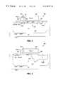
- FIG. 3is a cross-sectional view illustrating an EPROM or flash EPROM cell 300 in accordance with the present invention.
- FIG. 4is a cross-sectional diagram illustrating an EPROM or flash EPROM cell 400 in accordance with a first alternate embodiment of the present invention.
- FIG. 3shows a cross-sectional view that illustrates an EPROM or flash EPROM cell 300 in accordance with the present invention.
- cell 300is formed in a p-type semiconductor material 310 , such as a p ⁇ substrate 310 A or a p-well 310 B formed in a n ⁇ substrate 310 C, and includes n+ spaced-apart source and drain regions 312 and 314 , respectively, which are formed in material 310 .
- Cell 300also includes a channel region 316 which is defined in material 310 between source and drain regions 312 and 314 , and a layer of gate isolation material 320 which is formed on material 310 over channel region 316 .
- Channel region 316in turn, has a first channel region 316 A, a second channel region 316 B, and a third channel region 316 C.
- gate isolation layer 320is implemented with a first layer of oxide, a layer of nitride which is formed over the first oxide layer, and a second layer of oxide which is formed over the layer of nitride.
- This three layer structurewhich is known as ONO, is typically used as an interpoly dielectric in non-volatile floating-gate memory cells.
- the first oxide layeris formed to be approximately 20-100 ⁇ thick
- the nitride layeris formed to be approximately 50-200 ⁇ thick
- the second oxide layeris formed to be approximately 30-100 ⁇ thick.
- the first oxide layeris formed to be approximately 20-100 ⁇ thick
- the nitride layeris formed to be approximately 40-200 ⁇ thick
- the second oxide layeris formed to be approximately 30-100 ⁇ thick.
- cell 300further includes a first polysilicon (poly) gate 322 which is formed on gate isolation layer 320 over channel region 316 A, and an isolation region 324 , such as an oxide, which is formed on gate isolation layer 320 adjacent to gate 322 over channel region 316 B.
- a first polysilicon (poly) gate 322which is formed on gate isolation layer 320 over channel region 316 A
- an isolation region 324such as an oxide
- cell 300additionally includes a second poly gate 326 which is also formed on gate isolation layer 320 adjacent to isolation region 324 over channel region 316 C.
- second poly gate 326is shown as a poly spacer in FIG. 3, but may also have other, such as rectangular, shapes.
- cell 300is programmed by applying a programming voltage to gate 322 ; an intermediate voltage to drain region 314 , and ground to source region 312 .
- a low positive voltageis applied to second gate 326 .
- 3-10Vcan be applied to gate 322
- 3-7Vcan be applied to drain region 314
- 1.5-2.0Vcan be applied to second gate 326
- 2-10Vcan be applied to gate 322
- 2-7Vcan be applied to drain region 314
- 1-2Vcan be applied to second gate 326 .
- groundis applied to the substrate.
- a positive voltagesuch as the programming voltage
- the programming voltage applied to gate 322attracts electrons to the surface of channel region 316 to form a channel.
- the source-to-drain voltagesets up an electric field which has a maximum in second channel region 316 B.
- the width W of isolation region 324(and the corresponding second channel region 316 B) determines the strength of the electric field in second channel region 316 B. As the width W is reduced from the width that corresponds with the maximum electric field, the amount of source-side injection falls and eventually stops, while the amount of drain-side injection increases. On the other hand, as the width W is increased from the width that corresponds with the maximum electric field, the magnitude of the read current falls and eventually stops.
- the electric fieldcauses electrons to flow from source region 312 to drain region 314 via the channel. As the electrons flow to drain region 314 , the electric field accelerates these electrons into having ionizing collisions that form channel hot electrons near the junction of channel regions 316 A and 316 B.
- Nitridehas significantly more electron traps than hole traps and is thus capable of having a net negative charge.
- Cell 300is programmed when the number of electrons trapped in the nitride layer of ONO layer 320 produce a net negative charge which is sufficient to prevent a conductive channel from being formed when a read voltage is subsequently applied to gate 322 .
- Cell 300is read by applying the intermediate voltage to gate 322 and second gate 326 , and a read voltage to drain region 314 .
- Groundis applied to source region 312 .
- material 310is a substrate
- groundis applied to the substrate.
- material 310is a well
- groundis applied to the well while the intermediate voltage is applied to the substrate.
- cell 300When formed as a flash memory cell, cell 300 is erased by applying ground to gate 322 and second gate 326 , and the programming voltage to source and drain regions 312 and 314 .
- a negative voltagecan be applied to gate 322 and second gate 326 so that a positive voltage which is lower than the programming voltage can be applied to source and drain regions 312 and 314 .
- the voltage applied to source and drain regions 312 and 314is also applied to the p-substrate, or the p-well and n-substrate.
- FIG. 4shows a cross-sectional diagram that illustrates an EPROM or flash EPROM cell 400 in accordance with a first alternate embodiment.
- Cell 400is similar to cell 300 and, as a result, utilizes the same reference numerals to designate the structures which are common to both cells.
- cell 400differs from cell 300 in that cell 400 includes a lightly-doped drain (LDD) region 410 that is formed in material 310 while drain region 314 is formed in LDD region 410 .
- LDD region 410which reduces the strength of the electric field at the drain-to-material ( 310 ) junction, reduces the erase and read times.
Landscapes
- Engineering & Computer Science (AREA)
- Microelectronics & Electronic Packaging (AREA)
- Non-Volatile Memory (AREA)
- Semiconductor Memories (AREA)
Abstract
Description
1. Field of the Invention
The present invention relates to EPROM and flash memory cells and, more particularly, EPROM and flash memory cells with source-side injection and a gate dielectric that traps hot electrons during programming.
2. Description of the Related Art
An electrically-programmable read-only-memory (EPROM) cell and a flash memory cell are non-volatile memories that retain data stored in the cell after power to the cell has been removed. EPROM and flash memory cells principally differ from each other in that EPROM cells are erased with ultraviolet (UV) light, while flash cells are electrically erased.
FIG. 1 shows a cross-sectional view that illustrates a prior-art EPROM orflash memory cell 100. As shown in FIG. 1,cell 100 includes spaced-apart n+ source anddrain regions type substrate 110, and achannel region 116 which is defined insubstrate 110 between source anddrain regions
In addition,cell 100 also includes a layer ofgate oxide 120 which is formed overchannel region 116, and afloating gate 122 which is formed overgate oxide layer 120. Further,cell 100 additionally includes a layer of interpoly dielectric124 which is formed overfloating gate 122, and acontrol gate 126 which is formed overdielectric layer 124.
In addition, the drain-to-source voltage sets up an electric field which causes electrons to flow fromsource region 112 to drainregion 114 viachannel 130. As the electrons flow to drainregion 114, the electric field, which has a maximum neardrain region 114, accelerates these electrons into having ionizing collisions that form channel hot electrons neardrain region 114.
A small percentage of the channel hot electrons are then injected ontofloating gate 122 viagate oxide layer 120.Cell 100 is programmed when the number of electrons injected ontofloating gate 122 is sufficient to preventchannel 130 from being formed when a read voltage is subsequently applied tocontrol gate 126.
Since electrons are injected ontofloating gate 122 neardrain region 114,cell 100 is referred to as having drain-side injection. However, by altering the structure of the cell, electron injection can alternately take place near the source region.
When electrons are injected onto a floating gate near the source region, the cell is referred to as having source-side injection. U.S. Pat. No. 5,212,541 to Bergemont discloses a prior-art EPROM cell with source-side injection.
FIG. 2 shows a cross-sectional view that illustrates a source-sideinjection EPROM cell 200 as disclosed by the '541 patent. FIG. 2 is similar to FIG. 1 and, as a result, utilizes the same reference numerals to designate the structures which are common to both cells.
As shown in FIG. 2,cell 200 differs fromcell 100 in thatsource region 112 no longer lies directly below floatinggate 122 andcontrol gate 126, but instead is spaced apart from the region that lies directly below floating andcontrol gates
Further,cell 200 includes a polysilicon (poly)spacer 210 that is formed oversource region 112 and a portion ofchannel region 116, and is isolated fromsource region 112, the portion ofchannel region 116, floatinggate 122, andcontrol gate 126.
In operation,cell 200 is programmed in the same manner thatcell 100 is programmed except thatcell 200 also applies a low positive voltage topoly spacer 210. Under these biasing conditions, the structure ofcell 200 alters the drain-to-source electric field so that the electric field has a peak in the channel region that lies below the isolation region that separatespoly spacer 210 from floating andcontrol gates
As a result, channel hot electrons are formed in this channel region where a number of these hot electrons are injected ontofloating gate 122. As withcell 100,cell 200 is programmed when the number of electrons injected ontofloating gate 122 is sufficient to preventchannel 130 from being formed when a read voltage is subsequently applied to controlgate 126.
The present invention provides an electrically-programmable read-only-memory (EPROM) or a flash memory cell with source-side injection and a gate dielectric that traps hot electrons during programming.
The memory cell of the present invention, which is formed in a semiconductor material of a first conductivity type, includes spaced-apart source and drain regions of a second conductivity type which are formed in the material, and a channel region which is defined in the material between the source and drain regions. The channel region, in turn, has a first region, a second region, and a third region.
The cell also includes an isolation layer which is formed on the semiconductor material over the channel region. The isolation layer, in turn, includes a material, such as nitride, that has substantially more electron traps than hole traps so that the isolation layer is capable of having a negative potential which is sufficient to inhibit the formation of a conductive channel during a read operation.
The cell of the present invention also includes a first gate which is formed on the isolation layer over the first channel region, an isolation region which is formed on the isolation layer over the second channel region, and a second gate which is formed on the isolation layer over the third channel region.
The cell of the present invention is programmed by applying a programming voltage to the first gate, an intermediate voltage to the drain region, and a low positive voltage to the second gate. In addition, ground is applied to the source region and the semiconductor material.
The cell of the present invention is erased by applying a first erase voltage to the first gate, a second erase voltage to the drain region, and the first erase voltage to the second gate. In addition, ground is applied to the source region and the semiconductor material.
The cell of the present invention is read by applying a first read voltage to the first and second gates, and a second read voltage to the drain region. In addition, ground is applied to the source region and the semiconductor material.
A better understanding of the features and advantages of the present invention will be obtained by reference to the following detailed description and accompanying drawings which set forth an illustrative embodiment in which the principals of the invention are utilized.
FIG. 1 is a cross-sectional view illustrating a prior art EPROM orflash memory cell 100.
FIG. 2 is a cross-sectional view illustrating a source-sideinjection EPROM cell 200 as disclosed by U.S. Pat. No. 5,212,541 to Bergemont.
FIG. 3 is a cross-sectional view illustrating an EPROM orflash EPROM cell 300 in accordance with the present invention.
FIG. 4 is a cross-sectional diagram illustrating an EPROM orflash EPROM cell 400 in accordance with a first alternate embodiment of the present invention.
FIG. 3 shows a cross-sectional view that illustrates an EPROM orflash EPROM cell 300 in accordance with the present invention. As shown in FIG. 3,cell 300 is formed in a p-type semiconductor material 310, such as a p−substrate 310A or a p-well 310B formed in a n−substrate 310C, and includes n+ spaced-apart source anddrain regions material 310.
In accordance with the present invention,gate isolation layer 320 is implemented with a first layer of oxide, a layer of nitride which is formed over the first oxide layer, and a second layer of oxide which is formed over the layer of nitride. This three layer structure, which is known as ONO, is typically used as an interpoly dielectric in non-volatile floating-gate memory cells.
In a 0.35 micron photolithographic process, the first oxide layer is formed to be approximately 20-100 Å thick, the nitride layer is formed to be approximately 50-200 Å thick, and the second oxide layer is formed to be approximately 30-100 Å thick. Similarly, in a 0.25 micron photolithographic process, the first oxide layer is formed to be approximately 20-100 Å thick, the nitride layer is formed to be approximately 40-200 Å thick, and the second oxide layer is formed to be approximately 30-100 Å thick.
In addition,cell 300 further includes a first polysilicon (poly)gate 322 which is formed ongate isolation layer 320 overchannel region 316A, and anisolation region 324, such as an oxide, which is formed ongate isolation layer 320 adjacent togate 322 overchannel region 316B.
Further,cell 300 additionally includes asecond poly gate 326 which is also formed ongate isolation layer 320 adjacent toisolation region 324 overchannel region 316C. (Second gate 326 is shown as a poly spacer in FIG. 3, but may also have other, such as rectangular, shapes.)
In operation,cell 300 is programmed by applying a programming voltage togate 322; an intermediate voltage to drainregion 314, and ground tosource region 312. In addition, a low positive voltage is applied tosecond gate 326.
For example, in a 0.35 micron photolithographic process, 3-10V can be applied togate 322, 3-7V can be applied to drainregion 314, and 1.5-2.0V can be applied tosecond gate 326. Similarly, in a 0.25 micron photolithographic process, 2-10V can be applied togate 322, 2-7V can be applied to drainregion 314, and 1-2V can be applied tosecond gate 326.
Whenmaterial 310 is a p-substrate (source and drainregions material 310 is a p-well in a n-type substrate, ground is applied to the p-well while a positive voltage, such as the programming voltage, is applied to the substrate. This reverse-biases the well-to-substrate junction which, in turn, isolatescell 300 to avoid program/erase disturb when the cell is formed in an array.
The programming voltage applied togate 322 attracts electrons to the surface ofchannel region 316 to form a channel. In addition, the source-to-drain voltage sets up an electric field which has a maximum insecond channel region 316B.
The width W of isolation region324 (and the correspondingsecond channel region 316B) determines the strength of the electric field insecond channel region 316B. As the width W is reduced from the width that corresponds with the maximum electric field, the amount of source-side injection falls and eventually stops, while the amount of drain-side injection increases. On the other hand, as the width W is increased from the width that corresponds with the maximum electric field, the magnitude of the read current falls and eventually stops.
The electric field causes electrons to flow fromsource region 312 to drainregion 314 via the channel. As the electrons flow to drainregion 314, the electric field accelerates these electrons into having ionizing collisions that form channel hot electrons near the junction ofchannel regions
A small percentage of the channel hot electrons are then injected into the nitride layer ofONO layer 320 where the electrons are trapped. Nitride has significantly more electron traps than hole traps and is thus capable of having a net negative charge.
When formed as a flash memory cell,cell 300 is erased by applying ground togate 322 andsecond gate 326, and the programming voltage to source and drainregions gate 322 andsecond gate 326 so that a positive voltage which is lower than the programming voltage can be applied to source and drainregions regions
FIG. 4 shows a cross-sectional diagram that illustrates an EPROM orflash EPROM cell 400 in accordance with a first alternate embodiment.Cell 400 is similar tocell 300 and, as a result, utilizes the same reference numerals to designate the structures which are common to both cells.
As shown in FIG. 4,cell 400 differs fromcell 300 in thatcell 400 includes a lightly-doped drain (LDD)region 410 that is formed inmaterial 310 whiledrain region 314 is formed inLDD region 410.LDD region 410, which reduces the strength of the electric field at the drain-to-material (310) junction, reduces the erase and read times.
It should be understood that various alternatives to the embodiment of the invention described herein may be employed in practicing the invention. Thus, it is intended that the following claims define the scope of the invention and that methods and structures within the scope of these claims and their equivalents be covered thereby.
Claims (6)
1. A memory cell formed in a semiconductor material of a first conductivity type, the memory cell comprising:
a source region of a second conductivity type formed in the semiconductor material;
a drain region of the second conductivity type formed in the semiconductor material;
a channel region defined in the material between the source and drain regions, the channel region having a first region, a second region, and a third region;
a first isolation layer formed on the semiconductor material over the channel region;
a non-conductive layer formed on the first isolation layer, the non-conductive layer having a material not found in the first isolation layer, the non-conductive layer trapping a first number of electrons when the memory cell is programmed, and a second number of electrons when the memory cell is unprogrammed, the first number being different from the second number;
a second isolation layer formed on the nonconductive layer;
a first gate formed on the second isolation layer over the first channel region;
an isolation region formed on the second isolation layer over the second channel region; and
a second gate formed on the second isolation layer over the third channel region.
2. The cell of claim1 wherein a width of the isolation region is sized to allow source-side injection.
3. The cell of claim1 wherein a width of the isolation region is sized such that a drain-to-source electric field has a maximum strength near a junction of the first and second channel regions.
4. The cell of claim1 and further comprising a low-density drain region formed in the semiconductor material, wherein the drain region is formed in the low-density drain region.
5. The cell of claim1 wherein the nonconductive layer has a material not found in the second isolation layer.
6. The cell of claim1 wherein the first isolation layer is oxide, the non-conductive layer is nitride, and the second isolation layer is oxide.
Priority Applications (2)
| Application Number | Priority Date | Filing Date | Title |
|---|---|---|---|
| US09/316,445US6208557B1 (en) | 1999-05-21 | 1999-05-21 | EPROM and flash memory cells with source-side injection and a gate dielectric that traps hot electrons during programming |
| US09/665,612US6327187B1 (en) | 1999-05-21 | 2000-09-18 | EPROM and flash memory cells with source-side injection and a gate dielectric that traps hot electrons during programming |
Applications Claiming Priority (1)
| Application Number | Priority Date | Filing Date | Title |
|---|---|---|---|
| US09/316,445US6208557B1 (en) | 1999-05-21 | 1999-05-21 | EPROM and flash memory cells with source-side injection and a gate dielectric that traps hot electrons during programming |
Related Child Applications (1)
| Application Number | Title | Priority Date | Filing Date |
|---|---|---|---|
| US09/665,612DivisionUS6327187B1 (en) | 1999-05-21 | 2000-09-18 | EPROM and flash memory cells with source-side injection and a gate dielectric that traps hot electrons during programming |
Publications (1)
| Publication Number | Publication Date |
|---|---|
| US6208557B1true US6208557B1 (en) | 2001-03-27 |
Family
ID=23229072
Family Applications (2)
| Application Number | Title | Priority Date | Filing Date |
|---|---|---|---|
| US09/316,445Expired - LifetimeUS6208557B1 (en) | 1999-05-21 | 1999-05-21 | EPROM and flash memory cells with source-side injection and a gate dielectric that traps hot electrons during programming |
| US09/665,612Expired - LifetimeUS6327187B1 (en) | 1999-05-21 | 2000-09-18 | EPROM and flash memory cells with source-side injection and a gate dielectric that traps hot electrons during programming |
Family Applications After (1)
| Application Number | Title | Priority Date | Filing Date |
|---|---|---|---|
| US09/665,612Expired - LifetimeUS6327187B1 (en) | 1999-05-21 | 2000-09-18 | EPROM and flash memory cells with source-side injection and a gate dielectric that traps hot electrons during programming |
Country Status (1)
| Country | Link |
|---|---|
| US (2) | US6208557B1 (en) |
Cited By (74)
| Publication number | Priority date | Publication date | Assignee | Title |
|---|---|---|---|---|
| US6429063B1 (en)* | 1999-10-26 | 2002-08-06 | Saifun Semiconductors Ltd. | NROM cell with generally decoupled primary and secondary injection |
| US6525369B1 (en) | 2002-05-13 | 2003-02-25 | Ching-Yuan Wu | Self-aligned split-gate flash memory cell and its contactless flash memory arrays |
| US20030039153A1 (en)* | 2001-01-18 | 2003-02-27 | Eduardo Maayan | EEPROM array and method for operation thereof |
| US6528843B1 (en) | 2002-05-03 | 2003-03-04 | Silicon Based Technology Corp. | Self-aligned split-gate flash memory cell having a single-side tip-shaped floating-gate structure and its contactless flash memory arrays |
| US6531734B1 (en) | 2002-05-24 | 2003-03-11 | Silicon Based Technology Corp. | Self-aligned split-gate flash memory cell having an integrated source-side erase structure and its contactless flash memory arrays |
| US6570213B1 (en) | 2002-02-08 | 2003-05-27 | Silicon Based Technology Corp. | Self-aligned split-gate flash memory cell and its contactless NOR-type memory array |
| US20030206437A1 (en)* | 1995-03-07 | 2003-11-06 | California Institute Of Technology, A California Non-Profit Corporation | Floating-gate semiconductor structures |
| US20030235075A1 (en)* | 2002-06-21 | 2003-12-25 | Micron Technology, Inc. | Vertical NROM having a storage density of 1bit per 1F2 |
| US20040037127A1 (en)* | 2002-07-05 | 2004-02-26 | Impinj, Inc., A Delaware Corporation | Differential floating gate nonvolatile memories |
| US20040130934A1 (en)* | 2002-06-21 | 2004-07-08 | Micron Technology, Inc. | NROM memory cell, memory array, related devices and methods |
| US20040195593A1 (en)* | 2002-09-16 | 2004-10-07 | Impinj, Inc., A Delaware Corporation | Counteracting overtunneling in nonvolatile memory cells |
| US6830963B1 (en) | 2003-10-09 | 2004-12-14 | Micron Technology, Inc. | Fully depleted silicon-on-insulator CMOS logic |
| US20040265011A1 (en)* | 2003-06-30 | 2004-12-30 | Kiyonori Tsuda | Powder transport apparatus and image forming apparatus that can stabilize replenishment of powder |
| US20050001229A1 (en)* | 2003-07-01 | 2005-01-06 | Leonard Forbes | Apparatus and method for split transistor memory having improved endurance |
| US20050030794A1 (en)* | 2003-08-07 | 2005-02-10 | Micron Technology, Inc. | Method for erasing an NROM cell |
| US20050030792A1 (en)* | 2003-08-07 | 2005-02-10 | Micron Technology, Inc. | Method for programming and erasing an nrom cell |
| US20050030827A1 (en)* | 2002-09-16 | 2005-02-10 | Impinj, Inc., A Delaware Corporation | PMOS memory cell |
| US20050063235A1 (en)* | 2002-07-05 | 2005-03-24 | Impinj, Inc., A Delaware Corporation | PFET nonvolatile memory |
| US6878991B1 (en) | 2004-01-30 | 2005-04-12 | Micron Technology, Inc. | Vertical device 4F2 EEPROM memory |
| US20050105341A1 (en)* | 2003-11-04 | 2005-05-19 | Micron Technology, Inc. | NROM flash memory with self-aligned structural charge separation |
| US20050106811A1 (en)* | 2003-11-17 | 2005-05-19 | Micron Technology, Inc. | NROM flash memory devices on ultrathin silicon |
| US20050111257A1 (en)* | 1997-08-01 | 2005-05-26 | Boaz Eitan | Two bit non-volatile electrically erasable and programmable semiconductor memory cell utilizing asymmetrical charge trapping |
| US20050128804A1 (en)* | 2003-12-16 | 2005-06-16 | Micron Technology, Inc. | Multi-state NROM device |
| US20050133860A1 (en)* | 2003-12-17 | 2005-06-23 | Micron Technology, Inc. | Vertical NROM NAND flash memory array |
| US20050138262A1 (en)* | 2003-12-18 | 2005-06-23 | Micron Technology, Inc. | Flash memory having a high-permittivity tunnel dielectric |
| US20050173755A1 (en)* | 2004-02-10 | 2005-08-11 | Micron Technology, Inc. | NROM flash memory with a high-permittivity gate dielectric |
| US20050174847A1 (en)* | 2004-02-10 | 2005-08-11 | Micron Technology, Inc. | Nrom flash memory cell with integrated dram |
| US20050184337A1 (en)* | 2004-02-24 | 2005-08-25 | Micron Technology, Inc. | 4f2 eeprom nrom memory arrays with vertical devices |
| US20050212033A1 (en)* | 2004-03-24 | 2005-09-29 | Micron Technology, Inc. | Memory device with high dielectric constant gate dielectrics and metal floating gates |
| US20050247972A1 (en)* | 2004-05-06 | 2005-11-10 | Micron Technology, Inc. | Ballistic direct injection NROM cell on strained silicon structures |
| US20050253186A1 (en)* | 2003-09-05 | 2005-11-17 | Micron Technology, Inc. | Trench corner effect bidirectional flash memory cell |
| US6979857B2 (en) | 2003-07-01 | 2005-12-27 | Micron Technology, Inc. | Apparatus and method for split gate NROM memory |
| US20060068551A1 (en)* | 2004-09-27 | 2006-03-30 | Saifun Semiconductors, Ltd. | Method for embedding NROM |
| US20060124992A1 (en)* | 2003-12-16 | 2006-06-15 | Micron Technology, Inc. | NROM memory cell, memory array, related devices and methods |
| US7072217B2 (en) | 2004-02-24 | 2006-07-04 | Micron Technology, Inc. | Multi-state memory cell with asymmetric charge trapping |
| US7149118B2 (en) | 2002-09-16 | 2006-12-12 | Impinj, Inc. | Method and apparatus for programming single-poly pFET-based nonvolatile memory cells |
| US20070087503A1 (en)* | 2005-10-17 | 2007-04-19 | Saifun Semiconductors, Ltd. | Improving NROM device characteristics using adjusted gate work function |
| US7221138B2 (en) | 2005-09-27 | 2007-05-22 | Saifun Semiconductors Ltd | Method and apparatus for measuring charge pump output current |
| US20070141788A1 (en)* | 2005-05-25 | 2007-06-21 | Ilan Bloom | Method for embedding non-volatile memory with logic circuitry |
| US20070263456A1 (en)* | 2005-03-17 | 2007-11-15 | Impinj, Inc. | Inverter non-volatile memory cell and array system |
| US7317633B2 (en) | 2004-07-06 | 2008-01-08 | Saifun Semiconductors Ltd | Protection of NROM devices from charge damage |
| US7352627B2 (en) | 2006-01-03 | 2008-04-01 | Saifon Semiconductors Ltd. | Method, system, and circuit for operating a non-volatile memory array |
| US7369440B2 (en) | 2005-01-19 | 2008-05-06 | Saifun Semiconductors Ltd. | Method, circuit and systems for erasing one or more non-volatile memory cells |
| US20080136602A1 (en)* | 2005-03-31 | 2008-06-12 | Impinj, Inc. | Rfid tag with redundant non-volatile memory cell |
| US20080205150A1 (en)* | 2004-04-21 | 2008-08-28 | Impinj, Inc. | Hybrid non-volatile memory |
| US7420848B2 (en) | 2002-01-31 | 2008-09-02 | Saifun Semiconductors Ltd. | Method, system, and circuit for operating a non-volatile memory array |
| US7457183B2 (en) | 2003-09-16 | 2008-11-25 | Saifun Semiconductors Ltd. | Operating array cells with matched reference cells |
| US7466594B2 (en) | 2004-08-12 | 2008-12-16 | Saifun Semiconductors Ltd. | Dynamic matching of signal path and reference path for sensing |
| US7512009B2 (en) | 2001-04-05 | 2009-03-31 | Saifun Semiconductors Ltd. | Method for programming a reference cell |
| US7532529B2 (en) | 2004-03-29 | 2009-05-12 | Saifun Semiconductors Ltd. | Apparatus and methods for multi-level sensing in a memory array |
| US7535765B2 (en) | 2004-12-09 | 2009-05-19 | Saifun Semiconductors Ltd. | Non-volatile memory device and method for reading cells |
| US7605579B2 (en) | 2006-09-18 | 2009-10-20 | Saifun Semiconductors Ltd. | Measuring and controlling current consumption and output current of charge pumps |
| US7638835B2 (en) | 2006-02-28 | 2009-12-29 | Saifun Semiconductors Ltd. | Double density NROM with nitride strips (DDNS) |
| US7638850B2 (en) | 2004-10-14 | 2009-12-29 | Saifun Semiconductors Ltd. | Non-volatile memory structure and method of fabrication |
| US7668017B2 (en) | 2005-08-17 | 2010-02-23 | Saifun Semiconductors Ltd. | Method of erasing non-volatile memory cells |
| US7675782B2 (en) | 2002-10-29 | 2010-03-09 | Saifun Semiconductors Ltd. | Method, system and circuit for programming a non-volatile memory array |
| US7692961B2 (en) | 2006-02-21 | 2010-04-06 | Saifun Semiconductors Ltd. | Method, circuit and device for disturb-control of programming nonvolatile memory cells by hot-hole injection (HHI) and by channel hot-electron (CHE) injection |
| US7701779B2 (en) | 2006-04-27 | 2010-04-20 | Sajfun Semiconductors Ltd. | Method for programming a reference cell |
| US7738304B2 (en) | 2002-07-10 | 2010-06-15 | Saifun Semiconductors Ltd. | Multiple use memory chip |
| US7743230B2 (en) | 2003-01-31 | 2010-06-22 | Saifun Semiconductors Ltd. | Memory array programming circuit and a method for using the circuit |
| US7760554B2 (en) | 2006-02-21 | 2010-07-20 | Saifun Semiconductors Ltd. | NROM non-volatile memory and mode of operation |
| US7786512B2 (en) | 2005-07-18 | 2010-08-31 | Saifun Semiconductors Ltd. | Dense non-volatile memory array and method of fabrication |
| US7796450B1 (en) | 2007-04-24 | 2010-09-14 | Virage Logic Corporation | Radio frequency (RFID) tag including configurable single bit/dual bits memory |
| US7808818B2 (en) | 2006-01-12 | 2010-10-05 | Saifun Semiconductors Ltd. | Secondary injection for NROM |
| US8053812B2 (en) | 2005-03-17 | 2011-11-08 | Spansion Israel Ltd | Contact in planar NROM technology |
| US8102007B1 (en) | 2001-08-13 | 2012-01-24 | Synopsys, Inc. | Apparatus for trimming high-resolution digital-to-analog converter |
| US8111558B2 (en) | 2004-05-05 | 2012-02-07 | Synopsys, Inc. | pFET nonvolatile memory |
| US8122307B1 (en) | 2006-08-15 | 2012-02-21 | Synopsys, Inc. | One time programmable memory test structures and methods |
| US8139411B1 (en) | 2008-05-22 | 2012-03-20 | Synopsys, Inc. | pFET nonvolatile memory |
| US8253452B2 (en) | 2006-02-21 | 2012-08-28 | Spansion Israel Ltd | Circuit and method for powering up an integrated circuit and an integrated circuit utilizing same |
| US20150263022A1 (en)* | 2014-03-12 | 2015-09-17 | Kabushiki Kaisha Toshiba | Semiconductor memory device and manufacturing method thereof |
| US9875976B2 (en)* | 2015-12-31 | 2018-01-23 | Taiwan Semiconductor Manufacturing Company Ltd. | Switching device |
| US20180342285A1 (en)* | 2017-05-26 | 2018-11-29 | SK Hynix Inc. | Semiconductor device, semiconductor system including the same and operating method for a semiconductor system |
| US20230047688A1 (en)* | 2021-08-10 | 2023-02-16 | Powerchip Semiconductor Manufacturing Corporation | Memory structure |
Families Citing this family (6)
| Publication number | Priority date | Publication date | Assignee | Title |
|---|---|---|---|---|
| US6903977B2 (en)* | 2001-09-25 | 2005-06-07 | Sony Corporation | Nonvolatile semiconductor memory device and method of producing the same |
| TW519734B (en)* | 2001-12-04 | 2003-02-01 | Macronix Int Co Ltd | Programming and erasing methods of non-volatile memory having nitride tunneling layer |
| KR100464442B1 (en)* | 2003-01-11 | 2005-01-03 | 삼성전자주식회사 | Cell structure of EPROM device and fabrication thereof |
| KR20100080243A (en)* | 2008-12-31 | 2010-07-08 | 주식회사 동부하이텍 | Semiconductor device and fabricating method thereof |
| US10431265B2 (en) | 2017-03-23 | 2019-10-01 | Silicon Storage Technology, Inc. | Address fault detection in a flash memory system |
| FI127861B (en) | 2017-06-29 | 2019-04-15 | Labmaster Oy | Method and apparatus for dynamically generating hot electrons in aqueous solutions |
Citations (9)
| Publication number | Priority date | Publication date | Assignee | Title |
|---|---|---|---|---|
| US5168465A (en)* | 1988-06-08 | 1992-12-01 | Eliyahou Harari | Highly compact EPROM and flash EEPROM devices |
| US5284784A (en)* | 1991-10-02 | 1994-02-08 | National Semiconductor Corporation | Buried bit-line source-side injection flash memory cell |
| US5338952A (en)* | 1991-06-07 | 1994-08-16 | Sharp Kabushiki Kaisha | Non-volatile memory |
| US5394360A (en)* | 1990-07-06 | 1995-02-28 | Sharp Kabushiki Kaisha | Non-volatile large capacity high speed memory with electron injection from a source into a floating gate |
| US5402371A (en)* | 1992-10-09 | 1995-03-28 | Oki Electric Industry Co., Ltd. | Method of writing data into and erasing the same from semiconductor nonvolatile memory |
| US5422504A (en)* | 1994-05-02 | 1995-06-06 | Motorola Inc. | EEPROM memory device having a sidewall spacer floating gate electrode and process |
| US5455792A (en)* | 1994-09-09 | 1995-10-03 | Yi; Yong-Wan | Flash EEPROM devices employing mid channel injection |
| US5768192A (en) | 1996-07-23 | 1998-06-16 | Saifun Semiconductors, Ltd. | Non-volatile semiconductor memory cell utilizing asymmetrical charge trapping |
| US6011725A (en) | 1997-08-01 | 2000-01-04 | Saifun Semiconductors, Ltd. | Two bit non-volatile electrically erasable and programmable semiconductor memory cell utilizing asymmetrical charge trapping |
Family Cites Families (4)
| Publication number | Priority date | Publication date | Assignee | Title |
|---|---|---|---|---|
| US4794565A (en) | 1986-09-15 | 1988-12-27 | The Regents Of The University Of California | Electrically programmable memory device employing source side injection |
| US5212541A (en) | 1991-04-18 | 1993-05-18 | National Semiconductor Corporation | Contactless, 5v, high speed eprom/flash eprom array utilizing cells programmed using source side injection |
| US5912843A (en)* | 1996-03-18 | 1999-06-15 | Integrated Memory Technologies, Inc. | Scalable flash EEPROM memory cell, method of manufacturing and operation thereof |
| US5943261A (en)* | 1998-08-07 | 1999-08-24 | Winbond Electronics Corporation | Method for programming a flash memory |
- 1999
- 1999-05-21USUS09/316,445patent/US6208557B1/ennot_activeExpired - Lifetime
- 2000
- 2000-09-18USUS09/665,612patent/US6327187B1/ennot_activeExpired - Lifetime
Patent Citations (9)
| Publication number | Priority date | Publication date | Assignee | Title |
|---|---|---|---|---|
| US5168465A (en)* | 1988-06-08 | 1992-12-01 | Eliyahou Harari | Highly compact EPROM and flash EEPROM devices |
| US5394360A (en)* | 1990-07-06 | 1995-02-28 | Sharp Kabushiki Kaisha | Non-volatile large capacity high speed memory with electron injection from a source into a floating gate |
| US5338952A (en)* | 1991-06-07 | 1994-08-16 | Sharp Kabushiki Kaisha | Non-volatile memory |
| US5284784A (en)* | 1991-10-02 | 1994-02-08 | National Semiconductor Corporation | Buried bit-line source-side injection flash memory cell |
| US5402371A (en)* | 1992-10-09 | 1995-03-28 | Oki Electric Industry Co., Ltd. | Method of writing data into and erasing the same from semiconductor nonvolatile memory |
| US5422504A (en)* | 1994-05-02 | 1995-06-06 | Motorola Inc. | EEPROM memory device having a sidewall spacer floating gate electrode and process |
| US5455792A (en)* | 1994-09-09 | 1995-10-03 | Yi; Yong-Wan | Flash EEPROM devices employing mid channel injection |
| US5768192A (en) | 1996-07-23 | 1998-06-16 | Saifun Semiconductors, Ltd. | Non-volatile semiconductor memory cell utilizing asymmetrical charge trapping |
| US6011725A (en) | 1997-08-01 | 2000-01-04 | Saifun Semiconductors, Ltd. | Two bit non-volatile electrically erasable and programmable semiconductor memory cell utilizing asymmetrical charge trapping |
Non-Patent Citations (1)
| Title |
|---|
| Silicon Processing For The VLSI Era, vol. 2, Process Integration, Stanley Wolf Ph.D., Lattice Press, Sunset Beach, California, pp. 628-629. |
Cited By (220)
| Publication number | Priority date | Publication date | Assignee | Title |
|---|---|---|---|---|
| US20050104119A1 (en)* | 1995-03-07 | 2005-05-19 | California Institute Of Technology, A California Non-Profit Corporation | Floating-gate semiconductor structures |
| US6965142B2 (en) | 1995-03-07 | 2005-11-15 | Impinj, Inc. | Floating-gate semiconductor structures |
| US20050104118A1 (en)* | 1995-03-07 | 2005-05-19 | California Institute Of Technology, A California Non-Profit Corporation | Floating-gate semiconductor structures |
| US7548460B2 (en) | 1995-03-07 | 2009-06-16 | California Institute Of Technology | Floating-gate semiconductor structures |
| US20050099859A1 (en)* | 1995-03-07 | 2005-05-12 | California Institute Of Technology, A California Non-Profit Corporation | Floating-gate semiconductor structures |
| US20030206437A1 (en)* | 1995-03-07 | 2003-11-06 | California Institute Of Technology, A California Non-Profit Corporation | Floating-gate semiconductor structures |
| US7098498B2 (en) | 1995-03-07 | 2006-08-29 | California Institute Of Technology | Floating-gate semiconductor structures |
| US7116577B2 (en) | 1997-08-01 | 2006-10-03 | Saifun Semiconductors Ltd | Two bit non-volatile electrically erasable and programmable semiconductor memory cell utilizing asymmetrical charge trapping |
| US20050111257A1 (en)* | 1997-08-01 | 2005-05-26 | Boaz Eitan | Two bit non-volatile electrically erasable and programmable semiconductor memory cell utilizing asymmetrical charge trapping |
| US7405969B2 (en) | 1997-08-01 | 2008-07-29 | Saifun Semiconductors Ltd. | Non-volatile memory cell and non-volatile memory devices |
| US6429063B1 (en)* | 1999-10-26 | 2002-08-06 | Saifun Semiconductors Ltd. | NROM cell with generally decoupled primary and secondary injection |
| US7518908B2 (en) | 2001-01-18 | 2009-04-14 | Saifun Semiconductors Ltd. | EEPROM array and method for operation thereof |
| US20030039153A1 (en)* | 2001-01-18 | 2003-02-27 | Eduardo Maayan | EEPROM array and method for operation thereof |
| US7512009B2 (en) | 2001-04-05 | 2009-03-31 | Saifun Semiconductors Ltd. | Method for programming a reference cell |
| US8102007B1 (en) | 2001-08-13 | 2012-01-24 | Synopsys, Inc. | Apparatus for trimming high-resolution digital-to-analog converter |
| US7420848B2 (en) | 2002-01-31 | 2008-09-02 | Saifun Semiconductors Ltd. | Method, system, and circuit for operating a non-volatile memory array |
| US6570213B1 (en) | 2002-02-08 | 2003-05-27 | Silicon Based Technology Corp. | Self-aligned split-gate flash memory cell and its contactless NOR-type memory array |
| US6528843B1 (en) | 2002-05-03 | 2003-03-04 | Silicon Based Technology Corp. | Self-aligned split-gate flash memory cell having a single-side tip-shaped floating-gate structure and its contactless flash memory arrays |
| US6525369B1 (en) | 2002-05-13 | 2003-02-25 | Ching-Yuan Wu | Self-aligned split-gate flash memory cell and its contactless flash memory arrays |
| US6531734B1 (en) | 2002-05-24 | 2003-03-11 | Silicon Based Technology Corp. | Self-aligned split-gate flash memory cell having an integrated source-side erase structure and its contactless flash memory arrays |
| US20040202032A1 (en)* | 2002-06-21 | 2004-10-14 | Micron Technology, Inc. | Vertical NROM having a storage density of 1 bit per 1F2 |
| US6906953B2 (en) | 2002-06-21 | 2005-06-14 | Micron Technology, Inc. | Vertical NROM having a storage density of 1 bit per 1F2 |
| US6842370B2 (en) | 2002-06-21 | 2005-01-11 | Micron Technology, Inc. | Vertical NROM having a storage density of 1 bit per 1F2 |
| US8441056B2 (en) | 2002-06-21 | 2013-05-14 | Micron Technology, Inc. | NROM memory cell, memory array, related devices and methods |
| US20090010075A9 (en)* | 2002-06-21 | 2009-01-08 | Micron Technologies, Inc. | NROM memory cell, memory array, related devices and methods |
| US20040130934A1 (en)* | 2002-06-21 | 2004-07-08 | Micron Technology, Inc. | NROM memory cell, memory array, related devices and methods |
| US20090072303A9 (en)* | 2002-06-21 | 2009-03-19 | Micron Technology, Inc. | Nrom memory cell, memory array, related devices and methods |
| US20040066672A1 (en)* | 2002-06-21 | 2004-04-08 | Micron Technology, Inc. | Vertical NROM having a storage density of 1 bit per IF2 |
| US20050255647A1 (en)* | 2002-06-21 | 2005-11-17 | Micron Technology, Inc. | Vertical NROM having a storage density of 1 bit per 1F2 |
| US20030235075A1 (en)* | 2002-06-21 | 2003-12-25 | Micron Technology, Inc. | Vertical NROM having a storage density of 1bit per 1F2 |
| US7230848B2 (en) | 2002-06-21 | 2007-06-12 | Micron Technology, Inc. | Vertical NROM having a storage density of 1 bit per 1F2 |
| US6853587B2 (en) | 2002-06-21 | 2005-02-08 | Micron Technology, Inc. | Vertical NROM having a storage density of 1 bit per 1F2 |
| US7220634B2 (en) | 2002-06-21 | 2007-05-22 | Micron Technology, Inc. | NROM memory cell, memory array, related devices and methods |
| US7535048B2 (en) | 2002-06-21 | 2009-05-19 | Micron Technology, Inc. | NROM memory cell, memory array, related devices and methods |
| US20060126398A1 (en)* | 2002-06-21 | 2006-06-15 | Micron Technologies, Inc. | NROM memory cell, memory array, related devices and methods |
| US7541242B2 (en) | 2002-06-21 | 2009-06-02 | Micron Technology, Inc. | NROM memory cell, memory array, related devices and methods |
| US20060124998A1 (en)* | 2002-06-21 | 2006-06-15 | Micron Technology, Inc. | NROM memory cell, memory array, related devices and methods |
| US7221596B2 (en) | 2002-07-05 | 2007-05-22 | Impinj, Inc. | pFET nonvolatile memory |
| US20050063235A1 (en)* | 2002-07-05 | 2005-03-24 | Impinj, Inc., A Delaware Corporation | PFET nonvolatile memory |
| US20040037127A1 (en)* | 2002-07-05 | 2004-02-26 | Impinj, Inc., A Delaware Corporation | Differential floating gate nonvolatile memories |
| US6950342B2 (en) | 2002-07-05 | 2005-09-27 | Impinj, Inc. | Differential floating gate nonvolatile memories |
| US7738304B2 (en) | 2002-07-10 | 2010-06-15 | Saifun Semiconductors Ltd. | Multiple use memory chip |
| US7411829B2 (en) | 2002-09-16 | 2008-08-12 | Diorio Christopher J | Method and apparatus for programming single-poly pFET-based nonvolatile memory cells |
| US7573749B2 (en) | 2002-09-16 | 2009-08-11 | Virage Logic Corporation | Counteracting overtunneling in nonvolatile memory cells |
| US20070171724A1 (en)* | 2002-09-16 | 2007-07-26 | Impinj, Inc. | Counteracting overtunneling in nonvolatile memory cells |
| US20040195593A1 (en)* | 2002-09-16 | 2004-10-07 | Impinj, Inc., A Delaware Corporation | Counteracting overtunneling in nonvolatile memory cells |
| US7212446B2 (en) | 2002-09-16 | 2007-05-01 | Impinj, Inc. | Counteracting overtunneling in nonvolatile memory cells using charge extraction control |
| US20070019476A1 (en)* | 2002-09-16 | 2007-01-25 | Impinj, Inc., A Delaware Corporation | Method and apparatus for programming single-poly pFET-based nonvolatile memory cells |
| US20070019475A1 (en)* | 2002-09-16 | 2007-01-25 | Impinj, Inc., A Delaware Corporation | Method and apparatus for programming single-poly pFET-based nonvolatile memory cells |
| US20070019477A1 (en)* | 2002-09-16 | 2007-01-25 | Impinj, Inc., A Delaware Corporation | Method and apparatus for programming single-poly pFET-based nonvolatile memory cells |
| US7149118B2 (en) | 2002-09-16 | 2006-12-12 | Impinj, Inc. | Method and apparatus for programming single-poly pFET-based nonvolatile memory cells |
| US7408809B2 (en) | 2002-09-16 | 2008-08-05 | Impinj, Inc. | Method and apparatus for programming single-poly pFET-based nonvolatile memory cells |
| US7411828B2 (en) | 2002-09-16 | 2008-08-12 | Diorio Christopher J | Method and apparatus for programming single-poly pFET-based nonvolatile memory cells |
| US20050030827A1 (en)* | 2002-09-16 | 2005-02-10 | Impinj, Inc., A Delaware Corporation | PMOS memory cell |
| US7675782B2 (en) | 2002-10-29 | 2010-03-09 | Saifun Semiconductors Ltd. | Method, system and circuit for programming a non-volatile memory array |
| US7743230B2 (en) | 2003-01-31 | 2010-06-22 | Saifun Semiconductors Ltd. | Memory array programming circuit and a method for using the circuit |
| US20040265011A1 (en)* | 2003-06-30 | 2004-12-30 | Kiyonori Tsuda | Powder transport apparatus and image forming apparatus that can stabilize replenishment of powder |
| US20050001229A1 (en)* | 2003-07-01 | 2005-01-06 | Leonard Forbes | Apparatus and method for split transistor memory having improved endurance |
| US7095075B2 (en) | 2003-07-01 | 2006-08-22 | Micron Technology, Inc. | Apparatus and method for split transistor memory having improved endurance |
| US20060197143A1 (en)* | 2003-07-01 | 2006-09-07 | Micron Technology, Inc. | Apparatus and method for split transistor memory having improved endurance |
| US6979857B2 (en) | 2003-07-01 | 2005-12-27 | Micron Technology, Inc. | Apparatus and method for split gate NROM memory |
| US7719046B2 (en) | 2003-07-01 | 2010-05-18 | Micron Technology, Inc. | Apparatus and method for trench transistor memory having different gate dielectric thickness |
| US20050030794A1 (en)* | 2003-08-07 | 2005-02-10 | Micron Technology, Inc. | Method for erasing an NROM cell |
| US7272045B2 (en) | 2003-08-07 | 2007-09-18 | Micron Technology, Inc. | Method for programming and erasing an NROM cell |
| US7986555B2 (en) | 2003-08-07 | 2011-07-26 | Micron Technology, Inc. | Method for programming and erasing an NROM cell |
| US20070064466A1 (en)* | 2003-08-07 | 2007-03-22 | Micron Technology, Inc. | Method for programming and erasing an NROM cell |
| US20050141278A1 (en)* | 2003-08-07 | 2005-06-30 | Micron Technology, Inc. | Method for programming and erasing an NROM cell |
| US7088619B2 (en) | 2003-08-07 | 2006-08-08 | Micron Technology, Inc. | Method for programming and erasing an NROM cell |
| US20050174855A1 (en)* | 2003-08-07 | 2005-08-11 | Micron Technology, Inc. | Method for erasing an NROM cell |
| US20060133152A1 (en)* | 2003-08-07 | 2006-06-22 | Micron Technology, Inc. | Method for programming and erasing an NROM cell |
| US20050030792A1 (en)* | 2003-08-07 | 2005-02-10 | Micron Technology, Inc. | Method for programming and erasing an nrom cell |
| US20100067307A1 (en)* | 2003-08-07 | 2010-03-18 | Micron Technology, Inc. | Method for programming and erasing an nrom cell |
| US7075832B2 (en) | 2003-08-07 | 2006-07-11 | Micron Technology, Inc. | Method for erasing an NROM cell |
| US7075831B2 (en) | 2003-08-07 | 2006-07-11 | Micron Technology, Inc. | Method for erasing an NROM cell |
| US7639530B2 (en) | 2003-08-07 | 2009-12-29 | Micron Technology, Inc. | Method for programming and erasing an NROM cell |
| US7227787B2 (en) | 2003-08-07 | 2007-06-05 | Micron Technology, Inc. | Method for erasing an NROM cell |
| US6873550B2 (en) | 2003-08-07 | 2005-03-29 | Micron Technology, Inc. | Method for programming and erasing an NROM cell |
| US7277321B2 (en) | 2003-08-07 | 2007-10-02 | Micron Technology, Inc. | Method for programming and erasing an NROM cell |
| US7085170B2 (en) | 2003-08-07 | 2006-08-01 | Micron Technology, Ind. | Method for erasing an NROM cell |
| US7329920B2 (en) | 2003-09-05 | 2008-02-12 | Micron Technology, Inc. | Trench corner effect bidirectional flash memory cell |
| US7283394B2 (en) | 2003-09-05 | 2007-10-16 | Micron Technology, Inc. | Trench corner effect bidirectional flash memory cell |
| US6977412B2 (en) | 2003-09-05 | 2005-12-20 | Micron Technology, Inc. | Trench corner effect bidirectional flash memory cell |
| US7285821B2 (en) | 2003-09-05 | 2007-10-23 | Micron Technology, Inc. | Trench corner effect bidirectional flash memory cell |
| US20050253186A1 (en)* | 2003-09-05 | 2005-11-17 | Micron Technology, Inc. | Trench corner effect bidirectional flash memory cell |
| US20050255638A1 (en)* | 2003-09-05 | 2005-11-17 | Micron Technology, Inc. | Trench corner effect bidirectional flash memory cell |
| US7161217B2 (en) | 2003-09-05 | 2007-01-09 | Micron Technology, Inc. | Trench corner effect bidirectional flash memory cell |
| US20050258480A1 (en)* | 2003-09-05 | 2005-11-24 | Micron Technology, Inc. | Trench corner effect bidirectional flash memory cell |
| US7535054B2 (en) | 2003-09-05 | 2009-05-19 | Micron Technology, Inc. | Trench corner effect bidirectional flash memory cell |
| US20050269625A1 (en)* | 2003-09-05 | 2005-12-08 | Micron Technology, Inc. | Trench corner effect bidirectional flash memory cell |
| US7457183B2 (en) | 2003-09-16 | 2008-11-25 | Saifun Semiconductors Ltd. | Operating array cells with matched reference cells |
| US7973370B2 (en) | 2003-10-09 | 2011-07-05 | Micron Technology, Inc. | Fully depleted silicon-on-insulator CMOS logic |
| US6830963B1 (en) | 2003-10-09 | 2004-12-14 | Micron Technology, Inc. | Fully depleted silicon-on-insulator CMOS logic |
| US20050077564A1 (en)* | 2003-10-09 | 2005-04-14 | Micron Technology, Inc. | Fully depleted silicon-on-insulator CMOS logic |
| US7078770B2 (en) | 2003-10-09 | 2006-07-18 | Micron Technology, Inc. | Fully depleted silicon-on-insulator CMOS logic |
| US8174081B2 (en) | 2003-10-09 | 2012-05-08 | Micron Technology, Inc. | Fully depleted silicon-on-insulator CMOS logic |
| US20110204431A1 (en)* | 2003-10-09 | 2011-08-25 | Micron Technology, Inc. | Fully depleted silicon-on-insulator cmos logic |
| US20070109871A1 (en)* | 2003-11-04 | 2007-05-17 | Micron Technology, Inc. | NROM flash memory with self-aligned structural charge separation |
| US7480186B2 (en) | 2003-11-04 | 2009-01-20 | Micron Technology, Inc. | NROM flash memory with self-aligned structural charge separation |
| US7184315B2 (en) | 2003-11-04 | 2007-02-27 | Micron Technology, Inc. | NROM flash memory with self-aligned structural charge separation |
| US20050105341A1 (en)* | 2003-11-04 | 2005-05-19 | Micron Technology, Inc. | NROM flash memory with self-aligned structural charge separation |
| US20050106811A1 (en)* | 2003-11-17 | 2005-05-19 | Micron Technology, Inc. | NROM flash memory devices on ultrathin silicon |
| US8183625B2 (en) | 2003-11-17 | 2012-05-22 | Micron Technology, Inc. | NROM flash memory devices on ultrathin silicon |
| US7915669B2 (en) | 2003-11-17 | 2011-03-29 | Micron Technology, Inc. | NROM flash memory devices on ultrathin silicon |
| US20080203467A1 (en)* | 2003-11-17 | 2008-08-28 | Micron Technology, Inc. | Nrom flash memory devices on ultrathin silicon |
| US7358562B2 (en) | 2003-11-17 | 2008-04-15 | Micron Technology, Inc. | NROM flash memory devices on ultrathin silicon |
| US7378316B2 (en) | 2003-11-17 | 2008-05-27 | Micron Technology, Inc. | Method for fabricating semiconductor vertical NROM memory cells |
| US20100270610A1 (en)* | 2003-11-17 | 2010-10-28 | Micron Technology, Inc. | Nrom flash memory devices on ultrathin silicon |
| US7202523B2 (en) | 2003-11-17 | 2007-04-10 | Micron Technology, Inc. | NROM flash memory devices on ultrathin silicon |
| US20050280094A1 (en)* | 2003-11-17 | 2005-12-22 | Micron Technology, Inc. | NROM flash memory devices on ultrathin silicon |
| US20110163321A1 (en)* | 2003-11-17 | 2011-07-07 | Micron Technology, Inc. | Nrom flash memory devices on ultrathin silicon |
| US7276762B2 (en) | 2003-11-17 | 2007-10-02 | Micron Technology, Inc. | NROM flash memory devices on ultrathin silicon |
| US20050282334A1 (en)* | 2003-11-17 | 2005-12-22 | Micron Technology, Inc. | NROM flash memory devices on ultrathin silicon |
| US20050280089A1 (en)* | 2003-11-17 | 2005-12-22 | Micron Technology, Inc. | NROM flash memory devices on ultrathin silicon |
| US7244987B2 (en) | 2003-11-17 | 2007-07-17 | Micron Technology, Inc. | NROM flash memory devices on ultrathin silicon |
| US20070166927A1 (en)* | 2003-11-17 | 2007-07-19 | Micron Technology, Inc. | Nrom flash memory devices on ultrathin silicon |
| US20070170496A1 (en)* | 2003-11-17 | 2007-07-26 | Micron Technology, Inc. | Nrom flash memory devices on ultrathin silicon |
| US7768058B2 (en) | 2003-11-17 | 2010-08-03 | Micron Technology, Inc. | NROM flash memory devices on ultrathin silicon |
| US7276413B2 (en) | 2003-11-17 | 2007-10-02 | Micron Technology, Inc. | NROM flash memory devices on ultrathin silicon |
| US7238599B2 (en) | 2003-12-16 | 2007-07-03 | Micron Technology, Inc. | Multi-state NROM device |
| US20060128103A1 (en)* | 2003-12-16 | 2006-06-15 | Micron Technology, Inc. | NROM memory cell, memory array, related devices and methods |
| US20060166443A1 (en)* | 2003-12-16 | 2006-07-27 | Micron Technology, Inc. | Multi-state NROM device |
| US20050128804A1 (en)* | 2003-12-16 | 2005-06-16 | Micron Technology, Inc. | Multi-state NROM device |
| US7269071B2 (en) | 2003-12-16 | 2007-09-11 | Micron Technology, Inc. | NROM memory cell, memory array, related devices and methods |
| US7750389B2 (en) | 2003-12-16 | 2010-07-06 | Micron Technology, Inc. | NROM memory cell, memory array, related devices and methods |
| US20060152978A1 (en)* | 2003-12-16 | 2006-07-13 | Micron Technology, Inc. | Multi-state NROM device |
| US7371642B2 (en) | 2003-12-16 | 2008-05-13 | Micron Technology, Inc. | Multi-state NROM device |
| US20060124992A1 (en)* | 2003-12-16 | 2006-06-15 | Micron Technology, Inc. | NROM memory cell, memory array, related devices and methods |
| US20060124967A1 (en)* | 2003-12-16 | 2006-06-15 | Micron Technology, Inc. | NROM memory cell, memory array, related devices and methods |
| US7269072B2 (en) | 2003-12-16 | 2007-09-11 | Micron Technology, Inc. | NROM memory cell, memory array, related devices and methods |
| US7301804B2 (en) | 2003-12-16 | 2007-11-27 | Micro Technology, Inc. | NROM memory cell, memory array, related devices and methods |
| US7050330B2 (en) | 2003-12-16 | 2006-05-23 | Micron Technology, Inc. | Multi-state NROM device |
| US20060128104A1 (en)* | 2003-12-16 | 2006-06-15 | Micron Technology, Inc. | NROM memory cell, memory array, related devices and methods |
| US20060261404A1 (en)* | 2003-12-17 | 2006-11-23 | Micron Technology, Inc. | Vertical NROM NAND flash memory array |
| US7241654B2 (en) | 2003-12-17 | 2007-07-10 | Micron Technology, Inc. | Vertical NROM NAND flash memory array |
| US7339239B2 (en) | 2003-12-17 | 2008-03-04 | Micron Technology, Inc. | Vertical NROM NAND flash memory array |
| US20050133860A1 (en)* | 2003-12-17 | 2005-06-23 | Micron Technology, Inc. | Vertical NROM NAND flash memory array |
| US20050138262A1 (en)* | 2003-12-18 | 2005-06-23 | Micron Technology, Inc. | Flash memory having a high-permittivity tunnel dielectric |
| US20050277243A1 (en)* | 2003-12-18 | 2005-12-15 | Micron Technology, Inc. | Flash memory having a high-permittivity tunnel dielectric |
| US20090191676A1 (en)* | 2003-12-18 | 2009-07-30 | Micron Technology, Inc. | Flash memory having a high-permittivity tunnel dielectric |
| US7528037B2 (en) | 2003-12-18 | 2009-05-05 | Micron Technology, Inc. | Flash memory having a high-permittivity tunnel dielectric |
| US7157769B2 (en) | 2003-12-18 | 2007-01-02 | Micron Technology, Inc. | Flash memory having a high-permittivity tunnel dielectric |
| US7157771B2 (en) | 2004-01-30 | 2007-01-02 | Micron Technology, Inc. | Vertical device 4F2 EEPROM memory |
| US20060261405A1 (en)* | 2004-01-30 | 2006-11-23 | Micron Technology, Inc. | Vertical device 4F² eeprom memory |
| US20050167743A1 (en)* | 2004-01-30 | 2005-08-04 | Micron Technology, Inc. | Vertical device 4F2 EEPROM memory |
| US7332773B2 (en) | 2004-01-30 | 2008-02-19 | Micron Technology, Inc. | Vertical device 4F2 EEPROM memory |
| US6878991B1 (en) | 2004-01-30 | 2005-04-12 | Micron Technology, Inc. | Vertical device 4F2 EEPROM memory |
| US20050173755A1 (en)* | 2004-02-10 | 2005-08-11 | Micron Technology, Inc. | NROM flash memory with a high-permittivity gate dielectric |
| US6952366B2 (en) | 2004-02-10 | 2005-10-04 | Micron Technology, Inc. | NROM flash memory cell with integrated DRAM |
| US20050275011A1 (en)* | 2004-02-10 | 2005-12-15 | Micron Technology, Inc. | NROM flash memory with a high-permittivity gate dielectric |
| US20060019453A1 (en)* | 2004-02-10 | 2006-01-26 | Micron Technology, Inc. | NROM flash memory with a high-permittivity gate dielectric |
| US7221018B2 (en) | 2004-02-10 | 2007-05-22 | Micron Technology, Inc. | NROM flash memory with a high-permittivity gate dielectric |
| US7319613B2 (en) | 2004-02-10 | 2008-01-15 | Micron Technology, Inc. | NROM flash memory cell with integrated DRAM |
| US7479428B2 (en) | 2004-02-10 | 2009-01-20 | Leonard Forbes | NROM flash memory with a high-permittivity gate dielectric |
| US20050240867A1 (en)* | 2004-02-10 | 2005-10-27 | Micron Technology, Inc. | NROM flash memory cell with integrated DRAM |
| US20050174847A1 (en)* | 2004-02-10 | 2005-08-11 | Micron Technology, Inc. | Nrom flash memory cell with integrated dram |
| US7072213B2 (en) | 2004-02-10 | 2006-07-04 | Micron Technology, Inc. | NROM flash memory cell with integrated DRAM |
| US20060203555A1 (en)* | 2004-02-24 | 2006-09-14 | Micron Technology, Inc. | Multi-state memory cell with asymmetric charge trapping |
| US7072217B2 (en) | 2004-02-24 | 2006-07-04 | Micron Technology, Inc. | Multi-state memory cell with asymmetric charge trapping |
| US7616482B2 (en) | 2004-02-24 | 2009-11-10 | Micron Technology, Inc. | Multi-state memory cell with asymmetric charge trapping |
| US7911837B2 (en) | 2004-02-24 | 2011-03-22 | Micron Technology, Inc. | Multi-state memory cell with asymmetric charge trapping |
| US20050184337A1 (en)* | 2004-02-24 | 2005-08-25 | Micron Technology, Inc. | 4f2 eeprom nrom memory arrays with vertical devices |
| US7075146B2 (en) | 2004-02-24 | 2006-07-11 | Micron Technology, Inc. | 4F2 EEPROM NROM memory arrays with vertical devices |
| US20060203554A1 (en)* | 2004-02-24 | 2006-09-14 | Micron Technology, Inc. | Multi-state memory cell with asymmetric charge trapping |
| US7282762B2 (en) | 2004-02-24 | 2007-10-16 | Micron Technology, Inc. | 4F2 EEPROM NROM memory arrays with vertical devices |
| US7577027B2 (en) | 2004-02-24 | 2009-08-18 | Micron Technology, Inc. | Multi-state memory cell with asymmetric charge trapping |
| US20100039869A1 (en)* | 2004-02-24 | 2010-02-18 | Micron Technology, Inc. | Multi-state memory cell with asymmetric charge trapping |
| US7586144B2 (en) | 2004-03-24 | 2009-09-08 | Micron Technology, Inc. | Memory device with high dielectric constant gate dielectrics and metal floating gates |
| US20050280048A1 (en)* | 2004-03-24 | 2005-12-22 | Micron Technology, Inc. | Memory device with high dielectric constant gate dielectrics and metal floating gates |
| US7268031B2 (en) | 2004-03-24 | 2007-09-11 | Micron Technology, Inc. | Memory device with high dielectric constant gate dielectrics and metal floating gates |
| US20090294830A1 (en)* | 2004-03-24 | 2009-12-03 | Micron Technology, Inc. | Memory device with high dielectric constant gate dielectrics and metal floating gates |
| US8076714B2 (en) | 2004-03-24 | 2011-12-13 | Micron Technology, Inc. | Memory device with high dielectric constant gate dielectrics and metal floating gates |
| US20050212033A1 (en)* | 2004-03-24 | 2005-09-29 | Micron Technology, Inc. | Memory device with high dielectric constant gate dielectrics and metal floating gates |
| US20060237775A1 (en)* | 2004-03-24 | 2006-10-26 | Micron Technology, Inc. | Memory device with high dielectric constant gate dielectrics and metal floating gates |
| US7102191B2 (en) | 2004-03-24 | 2006-09-05 | Micron Technologies, Inc. | Memory device with high dielectric constant gate dielectrics and metal floating gates |
| US7550339B2 (en) | 2004-03-24 | 2009-06-23 | Micron Technology, Inc. | Memory device with high dielectric constant gate dielectrics and metal floating gates |
| US7532529B2 (en) | 2004-03-29 | 2009-05-12 | Saifun Semiconductors Ltd. | Apparatus and methods for multi-level sensing in a memory array |
| US8077511B2 (en) | 2004-04-21 | 2011-12-13 | Synopsys, Inc. | Hybrid non-volatile memory |
| US20080205150A1 (en)* | 2004-04-21 | 2008-08-28 | Impinj, Inc. | Hybrid non-volatile memory |
| US8111558B2 (en) | 2004-05-05 | 2012-02-07 | Synopsys, Inc. | pFET nonvolatile memory |
| US7683424B2 (en) | 2004-05-06 | 2010-03-23 | Micron Technology, Inc. | Ballistic direct injection NROM cell on strained silicon structures |
| US20050247972A1 (en)* | 2004-05-06 | 2005-11-10 | Micron Technology, Inc. | Ballistic direct injection NROM cell on strained silicon structures |
| US7274068B2 (en) | 2004-05-06 | 2007-09-25 | Micron Technology, Inc. | Ballistic direct injection NROM cell on strained silicon structures |
| US7859046B2 (en) | 2004-05-06 | 2010-12-28 | Micron Technology, Inc. | Ballistic direct injection NROM cell on strained silicon structures |
| US20060214220A1 (en)* | 2004-05-06 | 2006-09-28 | Micron Technology, Inc. | Ballistic direct injection NROM cell on strained silicon structures |
| US7317633B2 (en) | 2004-07-06 | 2008-01-08 | Saifun Semiconductors Ltd | Protection of NROM devices from charge damage |
| US7466594B2 (en) | 2004-08-12 | 2008-12-16 | Saifun Semiconductors Ltd. | Dynamic matching of signal path and reference path for sensing |
| US20060068551A1 (en)* | 2004-09-27 | 2006-03-30 | Saifun Semiconductors, Ltd. | Method for embedding NROM |
| US7964459B2 (en) | 2004-10-14 | 2011-06-21 | Spansion Israel Ltd. | Non-volatile memory structure and method of fabrication |
| US7638850B2 (en) | 2004-10-14 | 2009-12-29 | Saifun Semiconductors Ltd. | Non-volatile memory structure and method of fabrication |
| US7535765B2 (en) | 2004-12-09 | 2009-05-19 | Saifun Semiconductors Ltd. | Non-volatile memory device and method for reading cells |
| US7468926B2 (en) | 2005-01-19 | 2008-12-23 | Saifun Semiconductors Ltd. | Partial erase verify |
| US7369440B2 (en) | 2005-01-19 | 2008-05-06 | Saifun Semiconductors Ltd. | Method, circuit and systems for erasing one or more non-volatile memory cells |
| US8053812B2 (en) | 2005-03-17 | 2011-11-08 | Spansion Israel Ltd | Contact in planar NROM technology |
| US7791950B2 (en) | 2005-03-17 | 2010-09-07 | Virage Logic Corporation | Inverter non-volatile memory cell and array system |
| US20070263456A1 (en)* | 2005-03-17 | 2007-11-15 | Impinj, Inc. | Inverter non-volatile memory cell and array system |
| US7679957B2 (en) | 2005-03-31 | 2010-03-16 | Virage Logic Corporation | Redundant non-volatile memory cell |
| US20080136602A1 (en)* | 2005-03-31 | 2008-06-12 | Impinj, Inc. | Rfid tag with redundant non-volatile memory cell |
| US7808823B2 (en) | 2005-03-31 | 2010-10-05 | Virage Logic Corporation | RFID tag with redundant non-volatile memory cell |
| US20070141788A1 (en)* | 2005-05-25 | 2007-06-21 | Ilan Bloom | Method for embedding non-volatile memory with logic circuitry |
| US7786512B2 (en) | 2005-07-18 | 2010-08-31 | Saifun Semiconductors Ltd. | Dense non-volatile memory array and method of fabrication |
| US7668017B2 (en) | 2005-08-17 | 2010-02-23 | Saifun Semiconductors Ltd. | Method of erasing non-volatile memory cells |
| US7221138B2 (en) | 2005-09-27 | 2007-05-22 | Saifun Semiconductors Ltd | Method and apparatus for measuring charge pump output current |
| US20070087503A1 (en)* | 2005-10-17 | 2007-04-19 | Saifun Semiconductors, Ltd. | Improving NROM device characteristics using adjusted gate work function |
| US7352627B2 (en) | 2006-01-03 | 2008-04-01 | Saifon Semiconductors Ltd. | Method, system, and circuit for operating a non-volatile memory array |
| US7808818B2 (en) | 2006-01-12 | 2010-10-05 | Saifun Semiconductors Ltd. | Secondary injection for NROM |
| US8253452B2 (en) | 2006-02-21 | 2012-08-28 | Spansion Israel Ltd | Circuit and method for powering up an integrated circuit and an integrated circuit utilizing same |
| US7760554B2 (en) | 2006-02-21 | 2010-07-20 | Saifun Semiconductors Ltd. | NROM non-volatile memory and mode of operation |
| US7692961B2 (en) | 2006-02-21 | 2010-04-06 | Saifun Semiconductors Ltd. | Method, circuit and device for disturb-control of programming nonvolatile memory cells by hot-hole injection (HHI) and by channel hot-electron (CHE) injection |
| US7638835B2 (en) | 2006-02-28 | 2009-12-29 | Saifun Semiconductors Ltd. | Double density NROM with nitride strips (DDNS) |
| US7701779B2 (en) | 2006-04-27 | 2010-04-20 | Sajfun Semiconductors Ltd. | Method for programming a reference cell |
| US8122307B1 (en) | 2006-08-15 | 2012-02-21 | Synopsys, Inc. | One time programmable memory test structures and methods |
| US7605579B2 (en) | 2006-09-18 | 2009-10-20 | Saifun Semiconductors Ltd. | Measuring and controlling current consumption and output current of charge pumps |
| US7796450B1 (en) | 2007-04-24 | 2010-09-14 | Virage Logic Corporation | Radio frequency (RFID) tag including configurable single bit/dual bits memory |
| US8139411B1 (en) | 2008-05-22 | 2012-03-20 | Synopsys, Inc. | pFET nonvolatile memory |
| US20150263022A1 (en)* | 2014-03-12 | 2015-09-17 | Kabushiki Kaisha Toshiba | Semiconductor memory device and manufacturing method thereof |
| US9875976B2 (en)* | 2015-12-31 | 2018-01-23 | Taiwan Semiconductor Manufacturing Company Ltd. | Switching device |
| US20180342285A1 (en)* | 2017-05-26 | 2018-11-29 | SK Hynix Inc. | Semiconductor device, semiconductor system including the same and operating method for a semiconductor system |
| US11373698B2 (en)* | 2017-05-26 | 2022-06-28 | SK Hynix Inc. | Semiconductor device, semiconductor system including the same and operating method for a semiconductor system |
| US20230047688A1 (en)* | 2021-08-10 | 2023-02-16 | Powerchip Semiconductor Manufacturing Corporation | Memory structure |
| US11825655B2 (en)* | 2021-08-10 | 2023-11-21 | Powerchip Semiconductor Manufacturing Corporation | Memory structure |
Also Published As
| Publication number | Publication date |
|---|---|
| US6327187B1 (en) | 2001-12-04 |
Similar Documents
| Publication | Publication Date | Title |
|---|---|---|
| US6208557B1 (en) | EPROM and flash memory cells with source-side injection and a gate dielectric that traps hot electrons during programming | |
| US8174063B2 (en) | Non-volatile semiconductor memory device with intrinsic charge trapping layer | |
| US4958321A (en) | One transistor flash EPROM cell | |
| US6747310B2 (en) | Flash memory cells with separated self-aligned select and erase gates, and process of fabrication | |
| US7057931B2 (en) | Flash memory programming using gate induced junction leakage current | |
| US5824584A (en) | Method of making and accessing split gate memory device | |
| US6621115B2 (en) | Scalable flash EEPROM memory cell with floating gate spacer wrapped by control gate | |
| JP3055426B2 (en) | EEPROM cell having isolation transistor and method of manufacturing and operating the same | |
| US7407857B2 (en) | Method of making a scalable flash EEPROM memory cell with notched floating gate and graded source region | |
| US6828618B2 (en) | Split-gate thin-film storage NVM cell | |
| US6190968B1 (en) | Method for forming EPROM and flash memory cells with source-side injection | |
| US6482708B2 (en) | Nonvolatile memory device and method for manufacturing the same | |
| KR100192546B1 (en) | Flash memory and its manufacturing method | |
| US5457061A (en) | Method of making top floating-gate flash EEPROM structure | |
| US5972753A (en) | Method of self-align cell edge implant to reduce leakage current and improve program speed in split-gate flash | |
| US6313498B1 (en) | Flash memory cell with thin floating gate with rounded side wall, and fabrication process | |
| US20050285184A1 (en) | Flash memory device and method for programming/erasing the same | |
| GB2200795A (en) | Eprom cell with integral select transistor | |
| US7652320B2 (en) | Non-volatile memory device having improved band-to-band tunneling induced hot electron injection efficiency and manufacturing method thereof | |
| JP3111090B2 (en) | Method for fabricating non-volatile memory cell | |
| US7439572B2 (en) | Stacked gate memory cell with erase to gate, array, and method of manufacturing | |
| US20060226467A1 (en) | P-channel charge trapping memory device with sub-gate | |
| KR20050045753A (en) | Method of reading a non-volatile memory cell having a trapping dielectric layer |
Legal Events
| Date | Code | Title | Description |
|---|---|---|---|
| AS | Assignment | Owner name:NATIONAL SEMICONDUCTOR CORPORATION, CALIFORNIA Free format text:ASSIGNMENT OF ASSIGNORS INTEREST;ASSIGNORS:BERGEMONT, ALBERT;KALNITSKY, ALEXANDER;REEL/FRAME:009998/0759 Effective date:19990520 | |
| STCF | Information on status: patent grant | Free format text:PATENTED CASE | |
| FPAY | Fee payment | Year of fee payment:4 | |
| FPAY | Fee payment | Year of fee payment:8 | |
| FPAY | Fee payment | Year of fee payment:12 |