US6207472B1 - Low temperature thin film transistor fabrication - Google Patents
Low temperature thin film transistor fabricationDownload PDFInfo
- Publication number
- US6207472B1 US6207472B1US09/265,161US26516199AUS6207472B1US 6207472 B1US6207472 B1US 6207472B1US 26516199 AUS26516199 AUS 26516199AUS 6207472 B1US6207472 B1US 6207472B1
- Authority
- US
- United States
- Prior art keywords
- substrate
- gate
- depositing
- layer
- source
- Prior art date
- Legal status (The legal status is an assumption and is not a legal conclusion. Google has not performed a legal analysis and makes no representation as to the accuracy of the status listed.)
- Expired - Lifetime
Links
Images


Classifications
- H—ELECTRICITY
- H10—SEMICONDUCTOR DEVICES; ELECTRIC SOLID-STATE DEVICES NOT OTHERWISE PROVIDED FOR
- H10K—ORGANIC ELECTRIC SOLID-STATE DEVICES
- H10K10/00—Organic devices specially adapted for rectifying, amplifying, oscillating or switching; Organic capacitors or resistors having potential barriers
- H10K10/40—Organic transistors
- H10K10/46—Field-effect transistors, e.g. organic thin-film transistors [OTFT]
- H10K10/462—Insulated gate field-effect transistors [IGFETs]
- H10K10/468—Insulated gate field-effect transistors [IGFETs] characterised by the gate dielectrics
- H10K10/472—Insulated gate field-effect transistors [IGFETs] characterised by the gate dielectrics the gate dielectric comprising only inorganic materials
- H—ELECTRICITY
- H10—SEMICONDUCTOR DEVICES; ELECTRIC SOLID-STATE DEVICES NOT OTHERWISE PROVIDED FOR
- H10K—ORGANIC ELECTRIC SOLID-STATE DEVICES
- H10K10/00—Organic devices specially adapted for rectifying, amplifying, oscillating or switching; Organic capacitors or resistors having potential barriers
- H10K10/40—Organic transistors
- H10K10/46—Field-effect transistors, e.g. organic thin-film transistors [OTFT]
- H10K10/462—Insulated gate field-effect transistors [IGFETs]
- H10K10/466—Lateral bottom-gate IGFETs comprising only a single gate
- H—ELECTRICITY
- H01—ELECTRIC ELEMENTS
- H01L—SEMICONDUCTOR DEVICES NOT COVERED BY CLASS H10
- H01L21/00—Processes or apparatus adapted for the manufacture or treatment of semiconductor or solid state devices or of parts thereof
- H01L21/02—Manufacture or treatment of semiconductor devices or of parts thereof
- H01L21/02104—Forming layers
- H01L21/02107—Forming insulating materials on a substrate
- H01L21/02109—Forming insulating materials on a substrate characterised by the type of layer, e.g. type of material, porous/non-porous, pre-cursors, mixtures or laminates
- H01L21/02112—Forming insulating materials on a substrate characterised by the type of layer, e.g. type of material, porous/non-porous, pre-cursors, mixtures or laminates characterised by the material of the layer
- H01L21/02172—Forming insulating materials on a substrate characterised by the type of layer, e.g. type of material, porous/non-porous, pre-cursors, mixtures or laminates characterised by the material of the layer the material containing at least one metal element, e.g. metal oxides, metal nitrides, metal oxynitrides or metal carbides
- H01L21/02197—Forming insulating materials on a substrate characterised by the type of layer, e.g. type of material, porous/non-porous, pre-cursors, mixtures or laminates characterised by the material of the layer the material containing at least one metal element, e.g. metal oxides, metal nitrides, metal oxynitrides or metal carbides the material having a perovskite structure, e.g. BaTiO3
- H—ELECTRICITY
- H10—SEMICONDUCTOR DEVICES; ELECTRIC SOLID-STATE DEVICES NOT OTHERWISE PROVIDED FOR
- H10K—ORGANIC ELECTRIC SOLID-STATE DEVICES
- H10K85/00—Organic materials used in the body or electrodes of devices covered by this subclass
- H10K85/60—Organic compounds having low molecular weight
- H10K85/615—Polycyclic condensed aromatic hydrocarbons, e.g. anthracene
Definitions
- This inventionpertains to thin film field effect transistors (TFT), and in particular to the structure and processing of such TFT devices at a low, of the order of 150 degrees C., or less temperature.
- TFTthin film field effect transistors
- TFTThin film field effect transistors
- Thin film field effect transistorsuseful in flat panel display applications, at the current state of the art, involve a semiconductor layer with a channel defined by separated source and drain electrodes on one side and an insulated gate electrode on the other side that is centered with respect to the channel.
- the structure of the TFT deviceis usually fabricated through a set of serial deposition operations of carefully controlled layers on a substrate.
- the desired TFT electrical performanceinvolves low voltage operation with high carrier mobility in the channel, and with current vs voltage output characteristics that include a steep slope followed by a saturation region.
- the current TFT devicestypically use amorphous silicon (a—Si:H) as the semiconductor and silicon oxide and/or silicon nitride as the gate insulator.
- amorphous silicona—Si:H
- silicon oxide and/or silicon nitridesilicon oxide and/or silicon nitride
- the inventionbroadens the range of materials and processes available for TFT devices by providing in the device suture an organic semiconductor layer that is in contact with an inorganic mixed oxide gate insulator involving processing with the types of processing techniques that can take place in a temperature range from about room temperature to about 150 degrees C.
- a TFT of the inventionhas a pentacene semiconductor layer in contact with a barium zirconate titanate gate insulator layer formed on a polycarbonate transparent substrate employing at least one of the techniques of sputtering, spinning, evaporation and laser ablation.
- FIG. 1is a depiction of typical elements in a prior art type TFT device.
- FIGS. 2 to 5are depictions of the partial products at intermediate steps in the fabrication of a TFT in accordance with the present invention.
- FIG. 6is a depiction of all the elements in a TFT in accordance with the present invention.
- FIG. 7is a sketch of a room temperature sputter deposition processing apparatus.
- FIGS. 8 through 16are data plots of the examples of the present invention wherein:
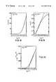
- FIGS. 8, 9 and 10show the operating characteristics of one example of a TFT device of the present invention.
- FIG. 8shows data on the organic semiconductor pentacene as the semiconductor and a 122 nm thick layer of barium zirconate titanate(BZT), deposited by room temperature sputtering, as the gate insulator; illustrating the dependence of the drain current on the gate voltage at a fixed source-drain voltage.
- BZTbarium zirconate titanate
- FIG. 9is a plot of the data from FIG. 8 in a semi logarithmic scale used to calculate the current modulation and sub-threshold slope.
- FIG. 10is a replot of the data from FIG. 9 as the square root of the drain current plotted versus the gate voltage in the saturation regime in order to calculate the field effect mobility.
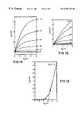
- FIGS. 11-15show operating characteristic data of a second example of a TFT device of the invention using the organic semiconductor pentacene as the semiconductor and a 122 nm thick layer of barium zirconate titanate deposited by room temperature sputtering, as the gate insulator.
- FIG. 11shows the dependence of the drain current on the gate voltage at a fixed source-drain voltage.
- FIG. 12is the plot of the data from FIG. 11 in a semi logarithmic scale used to calculate the current modulation and sub-threshold slope.
- FIG. 13is a plot of the data from FIG. 12 as the square root of the drain current as a function of the gate voltage in the saturation regime in order to calculate the field effect mobility.
- FIG. 14shows the dependence of the drain current on the source-drain voltage at different gate voltage levels
- FIG. 15is a plot of the drain current as a function of the gate voltage in the linear regime at a fixed drain voltage for calculation of the mobility in the linear regime of TFT operation.
- FIG. 16shows the dependence of the drain current on the source-drain voltage at different gate voltage levels, from a third example TFT device fabricated on a transparent polycarbonate substrate using pentacene as semiconductor and a 128 nm thick layer of barium zirconate titanate (BZT) deposited by room temperature sputtering as the gate insulator.
- BZTbarium zirconate titanate
- the TFT deviceis supported by an insulting substrate 1 with the device having a semiconductor region 2 with field effect transistor channel 3 defining, separated, source 4 and drain 5 on one side of the semiconductor region 2 , and a gate 6 electrode separated by insulation 7 from the channel 3 and centered with respect to the channel 3 on the other side of the semiconductor region 2 .
- the desired electrical performance of the deviceplaces stringent material and dimensional requirements on the layers and on the processing parameters in building the device.
- Many of the present devicesuse amorphous silicon (a—Si:H) as the semiconductor 2 , and conventional dielectric materials such as SiO, SiO 2 , or Si 3 N 4 , as the gate insulator 7 .
- the substrate 1is usually glass. The materials used and the processing that must be employed therewith, during fabrication of these devices result in temperature excursions in the several hundreds of degrees C. being required.
- room temperature vicinity type processeswhich are in the temperature range of about 25 to about 150 degrees C. and which has dielectric constant values of 15 and above, devices with acceptable TFT carrier mobility in the channel 3 can be produced; and further the room temperature vicinity type processes also permit broadening the range of available materials for substrate 1 to include thin and transparent plastics such as polycarbonate films.
- the room temperature vicinity type processesmay be considered to be those in which in the deposition and in any subsequent annealing type step the temperature is up to about 150 degrees C.; which temperature range is far below the 300-400 degree C. range presently used in the art. Such processes would include for examples sputtering, spinning, evaporation and laser ablation.
- FIGS. 2-6the partial product depictions illustrated in FIGS. 2-5 result in the novel TFT depicted in FIG. 6
- the TFT deviceis built on a substrate 10 which provides support for fabrication of the device on surface 11 and serves as a portion of the completed device.
- the substrateis held in the vicinity of room temperature (25 degrees C.) Silicon oxide, quartz and glass are satisfactory substrate and supporting materials; further, through the capabilities conferred by the invention the choices for a substrate material is broadened to include plastics such as polycarbonates which provide additional properties of impact resistance, lightness of weight and flexibility.
- the gate electrode 12is positioned on the surface 11 .
- the electrode 12is about 0.1 micrometer in thickness. Satisfactory materials are metals such as gold, silver, palladium, aluminum, copper and platinum and conducting polymers such as polyaniline and polypyrrole. The resistance of the electrodes and connecting members should be selected so that signal deterioration due to resistance is minimized.
- the gate dielectric member 13is of an inorganic oxide that is deposited on the surface 11 over the gate electrode 12 .
- the depositionis accomplished with one of the low temperature techniques of sputtering, spinning, evaporation and ablation, at a room temperature vicinity temperature range of about 25-150 degrees C.
- Suitable inorganic oxides at the present state of the artmay include Ta 2 O 3 , V 2 O 3 , TiO 2 , and the ferroelectric insulators Bi 4 Ti 3 O 12 , BaMgF 4 , SrTiO 3 , which within the class include the mixed oxides SrBi 2 Ta (1-x) Nb x O 3 , PbZr x Ti (1-x) O 3 , known in the art as (PZT), BaZr x Ti (1-x) O 3 , known in the art as (BZT), and Ba x Sr (1-x) TiO 3 , known in the art as (BST).
- the BZT materialhas received some background attention in the publication by Wu et al., in Appl. Phys. Lett. 69, 1996, pages 2659-2661.
- the gate dielectric 13is deposited to a thickness in the region 14 above the gate electrode 12 in the range of 0.5 micrometer.
- the room temperature vicinity of up to about 150 degrees C. deposition of inorganic gate oxide materialsprovides a device gate insulator with a dielectric constant in the range of 15 or above which is adequate to provide satisfactory carrier mobility in the being fabricated device channel.
- much higher dielectric constants around 300were involved and which required very high temperature annealing steps that were incompatible with some materials.
- the intended applications of those high dielectric constant deviceswere not displays but were devices built on silicon substrates.
- the organic semiconductor 15 of the TFT device of the inventionis deposited at a room temperature vicinity temperature, over the gate insulation layer 13 .
- a satisfactory organic semiconductor materialis the material pentacene, which in a TFT device can impart performance in which there is a field effect carrier mobility of about 0.6 cm 2 V ⁇ 1 sec ⁇ 1 in the channel, and current modulation of up to 10 8 at operating voltage ranges of up to ⁇ 100 V.
- the material pentacenehas received some background attention in the art as described in the following publications: Lin et al. IEEE 54th Annual Device Research Conference, 1996, Pages 80-81, Brown et al., J. Appl. Phys.
- the TFT of the inventionis depicted.
- the source 16 and drain 17 with the channel defining separation 18 centered over the gate 12are deposited in registration with the gate 12 on the exposed surface of the organic semiconductor member 15 using a low temperature deposition process at a room temperature vicinity temperature.
- the layers deposited and operated in the 25 to 150 degrees C. vicinity of room temperatureare well matched to the moderate dielectric needs of the organic semiconductors and enable processing and service with much lower temperature tolerant substrates, such as plastic.
- FIG. 7An illustration of the room temperature type deposition technique involving sputtering is provided in connection with the apparatus depicted in FIG. 7 .
- FIG. 7there is shown a schematic of a sputter deposition apparatus 20 that can be used to deposit the layer 13 of the invention using as a specific example the inorganic mixed oxide material Barium-Zirconate-Titanate (BZT).
- BZTBarium-Zirconate-Titanate
- the apparatus 20includes a sputtering chamber 21 , having a throttle valve 22 which separates the reactor chamber 21 from a vacuum pump not shown.
- a pressed powder BZT sputtering target 23such as is manufactured by PURE TECH, in Carmel N.Y., is mounted in the reactor chamber 21 .
- Permanent magnets 24are located on the backside of the target 23 to enhance plasma density during the sputtering.
- the sputtering target 23is electrically isolated from the housing 29 and electrically connected to a RF power supply 25 through an impedance matching device 26 .
- One or more substrates 27such as silicon wafers, glass plates or polycarbonate sheets, are mounted on a sample holder 28 which is isolated from the reactor chamber housing 29 by a dielectric spacer 30 .
- the housing 29is maintained at a selected temperature such as room temperature.
- the sample holder 28can be RF biased for plasma cleaning using a RF power supply 31 connected through an impedance matching device 32 .
- the substrate holder 28is also provided with rotation capability at 33 .
- the substrates 27have planetary rotation capability 34 to assure uniformity across the substrate being coated.
- the films deposited at room temperatureare well matched to the moderate dielectric needs of the organic semiconductor TFT's and enable broadening the range of useable substrates to include processing on plastic substrates.
- the reactor chamber 20also contains conduits 34 and 35 for introducing various gases.
- argoncould be introduced through conduit 34 and oxygen through conduit 35 .
- Gases employed in the following examples of the inventionshould have a purity greater than about 95.5%; with a purity in the range from about 98.5 to about 99.99% being preferred.
- the argon and oxygen gasesare introduced into the chamber by first passing them through separate flow controllers at a sufficient flow to provide a total pressure of Ar and oxygen from about 1 mTorr to 50 mTorr.
- the Ar and oxygen flowsare from about 100 to 1 sccm, more preferably the Ar flow is about 10 sccm and the oxygen flow about 2 sccm.
- the pressure of argon and oxygenbe about 2-3 mTorr.
- Such conditionscan also be obtained by premixing the Ar and oxygen in one gas cylinder providing the desired gas concentration.
- the argon and oxygen gasesare introduced as illustrated into the chamber through two separate flow controllers in conduits 34 and 35 .
- Suitable substrates which may be coated with the room temperature vicinity deposited layers or films of the inventioninclude materials such as plastic; metals; various types of glass; quartz; silicon wafers and the likes thereof.
- a substrate to be coatedmay be any shape or size compatible with being placed into asputtering chamber apparatus. Thus, regular or irregular shape objects having any dimension may be used and depending on the design of the sputtering system with modifications to the vacuum chamber, coatings can be applied to sheet materials fed in a roll to roll format. In operation, the substrate is mounted on the substrate holder inside the reactive sputtering chamber of the sputter system.
- the reactive sputtering chamberis then tightly sealed and evacuated until a pressure reading in the range of about 1 ⁇ 10 ⁇ 4 to about 1 ⁇ 10 ⁇ 7 Torr is obtained.
- the substrateis held at a constant, room temperature value of about 25 degrees C. throughout the entire deposition process.
- the substrate material usedmay be subjected to in-situ plasma cleaning; using for example H 2 , Ar, O 2 , or N 2 type plasma sputter etching techniques.
- the admixed gasesare introduced into the reaction sputter chamber at example flow rates of about 1 to 100 standard cubic centimeters per minute (sccm); with the flow rate of the Ar gas being at about 10 sccm and oxygen being at about 2 sccm.
- the gases in this examplewould be introduced into the reaction chamber at a pressure of about 1 to 20 mTorr; with an admixture pressure of about 3 mTorr. being preferred.
- an rf power density from about 0.05 to 4 W/cm 2would be applied to the example BZT target 23 throughout the deposition process. Most preferably, the rf power would be maintained at 0.8 W/cm 2 throughout the deposition process through the RF power supply source involving elements 25 and 26 .
- the BZT filmis deposited onto the substrate at a rate of about 10 Angstroms/min., such that an essential continuous coating of the film on the substrate is obtained. These conditions permit film depositions in thicknesses in a range of about 100 to 5000 Angstroms with about 1250 being preferred.
- examples 1, 2 and 3are provided that illustrate the deposition and the construction of the invention.
- a sputter deposition processis used as an example in connection with FIG. 7, the other room temperature vicinity type processes can be used.
- Substratessuch as silicon wafers with a blanket coating of 150 ⁇ titanium followed by 400 ⁇ of platinum can be loaded into a BZT sputter deposition chamber as descried in connection with FIG. 7 .
- the chamberis pumped down to a base pressure of 2.1 ⁇ 10 ⁇ 7 torr after which a flow of 10 standard cubic centemeters per minute (sccm) of argon and 2 sccm of oxygen gas are introduced into the chamber through elements 34 and 35 .
- sccmstandard cubic centemeters per minute
- a plasmais ignited in the chamber by applying a radio frequency ac voltage through elements 25 and 26 to the BZT sputter target 23 while maintaining the chamber at ground potential.
- the ions in the rf plasmathus created is used to reactively sputter the BZT from the target on to the samples 27 loaded in the chamber.
- a total power of 100 wattswhich corresponds to a power density of about 0.8 watts/cm 2 is employed to achieve a BZT thickness of about 1250 ⁇ .
- the wafersare unloaded at the end of the run and provided with an array of top electrode dots consisting of a bilayer of 5000 ⁇ Al/600 ⁇ Au deposited by electron beam evaporation through a metal mask in a different vacuum system. These parts are used to measure the dielectric constant and breakdown characteristics of the BZT films.
- the dielectric constantis 17.3 and the breakdown field about 1 MV/cm for BZT films of 1250 ⁇ thickness.
- the deposited BZT films at room temperaturethus range in thickness from 1000 to 2000 ⁇ with a dielectric constant in the range of 15 to 20 which can sustain fields of about 1 MV/cm without breakdown.
- TFT's having as gate insulator a thin film of barium zirconate titanate (BZT),are fabricated by means of room temperature vicinity type rf sputtering as described in Example 1 together with the TFT fabrication steps described in connection with FIGS. 2-6.
- oxidized silicon substratesare cleaned in an isopropanol bath using ultrasonic agitation and dried with nitrogen. They are then assembled with a metal mask with openings corresponding to the gate lines and placed and pumped down to high vacuum in an electron beam evaporator.
- Gate metallization of either 400 ⁇ of aluminum or a bilayer of 150 ⁇ of titanium followed by 300 ⁇ of platinumis deposited on the substrates by electron beam evaporation. Then a gate insulator film 13 of BZT is deposited on top of the gate 12 and the substrate surface 11 , as described in example 1.
- An organic semiconductor pentacene layer 15is deposited on the BZT gate insulator 13 using thermal evaporation in a vacuum chamber through a mask that separates individual devices from each other and reduces fringe currents which are currents that pass through the pentacene layer that is deposited outside the area of the devices. Satisfactory results are achieved with both the ultra high and the high vacuum chambers.
- the samplesmay then be assembled with a mask provided with openings for source and drain contact electrodes, placed and pumped down in an electron beam evaporator and coated with 600 ⁇ of gold to produce the source 16 and drain 17 contacts.
- the resulting TFT structureis shown schematically in FIG. 6 Alternatively, it will be apparent to one skilled in the art that the source 16 and drain 17 contacts can be placed on top of the insulator 13 and then the pentacene layer 15 placed over them.
- the pentacene film 15could be deposited using a soluble precursor of pentacene which is converted to pentacene by heating up to 140° C. in vacuo as described in the publication by A. R. Brown et al. in the J App. Phys., Volume 79, pg 2136, 1996.
- electrode materialssuch as molybdenum, tungsten, nickel, platinum, palladium, conducting polymers, oligomers and organic molecules.
- FIGS. 8, 9 and 10which are typical operating characteristics of a pentacene organic semiconductor TFT, with an inorganic mixed oxide gate dielectric of BZT as represented by the schematic drawing in FIG. 6, in which the thickness of the BZT gate-insulator is approximately 1220 ⁇ and its dielectric constant, is 17.3.
- the BZTis deposited by sputter deposition as described in connection with FIG. 7 .
- the source drain separation (channel length, L)is 18.4 ⁇ m and the channel width, W, is 1500 ⁇ m.
- FIGS. 8 and 9show the dependence of Drain Current (I D ) on Gate Voltage (V G ) in saturation.
- FIG. 10shows a plot of the square root of I D VS V G .
- the field effect mobility, ⁇is calculated from the slope of the plot to be 0.32 cm 2 V ⁇ 1 sec ⁇ 1 .
- the current modulationis about 10 5 for a gate voltage variation of 19 volts (+5 to ⁇ 14 V).
- the sub-threshold slopeis approximately 2 volts per decade of current modulation.
- FIGS. 11, 12 and 13are depictions of data measured and plotted similarly to FIGS. 8 and 10 from another TFT device fabricated by the procedure described in connection with FIGS. 2-7; except that the channel length L is 11.2 ⁇ m and the width was 1500 ⁇ m. Calculated values of the various characteristic parameters are very close to the ones described in connection with FIGS. 8-10.
- FIGS. 14 and 15which are characteristics from another TFT device with a BZT gate insulator that is 1280 ⁇ thick and which has a channel length of 125 ⁇ m and a channel width of 500 ⁇ m.
- FIG. 14shows the measured drain current (I D ) vs the drain voltage (V D ) at various gate voltage levels showing the expected TFT behavior.
- FIG. 15shows the I D versus V G plot for this device in the linear regime rather than in the saturation regime as shown in FIGS. 8-10 and 11 - 13 .
- the mobility calculated from this linear regime analysisis 0.27 cm 2 V ⁇ 1 sec ⁇ 1 . All of these different characteristics are considered to be adequate for the use of such TFT's in display applications.
- Example 3illustrates the invention with plastic substrates.
- TFT devicesare fabricated on transparent polycarbonate substrates that are 0.020′′ thick which is about 0.5 mm using a sputtered BZT gate insulator that is about 1280 ⁇ in thickness deposited by the sputtering process as described in connection with FIG. 7 and using the steps described in connection with FIGS. 2-6 for depositing the other layers.
- FIG. 16shows the drain current versus drain voltage plot for a TFT device on this type of substrate with a channel length of 69 ⁇ m and channel width of 1500 ⁇ m.
- Mobility values as high as 0.38 cm 2 V ⁇ 1 sec ⁇ 1were measured from devices with a W/L ratio of 4. These are the highest reported mobilities from devices fabricated on plastic substrate, and they are obtained at a maximum gate voltage of 4 V and hence are well suited for display applications.
Landscapes
- Chemical & Material Sciences (AREA)
- Inorganic Chemistry (AREA)
- Thin Film Transistor (AREA)
- Electroluminescent Light Sources (AREA)
Abstract
Description
Claims (10)
Priority Applications (3)
| Application Number | Priority Date | Filing Date | Title |
|---|---|---|---|
| US09/265,161US6207472B1 (en) | 1999-03-09 | 1999-03-09 | Low temperature thin film transistor fabrication |
| JP2000064964AJP2000269515A (en) | 1999-03-09 | 2000-03-09 | Method for manufacturing low-temperature thin film transistor and transistor device |
| US09/740,721US20010015438A1 (en) | 1999-03-09 | 2000-12-18 | Low temperature thin film transistor fabrication |
Applications Claiming Priority (1)
| Application Number | Priority Date | Filing Date | Title |
|---|---|---|---|
| US09/265,161US6207472B1 (en) | 1999-03-09 | 1999-03-09 | Low temperature thin film transistor fabrication |
Related Child Applications (1)
| Application Number | Title | Priority Date | Filing Date |
|---|---|---|---|
| US09/740,721DivisionUS20010015438A1 (en) | 1999-03-09 | 2000-12-18 | Low temperature thin film transistor fabrication |
Publications (1)
| Publication Number | Publication Date |
|---|---|
| US6207472B1true US6207472B1 (en) | 2001-03-27 |
Family
ID=23009279
Family Applications (2)
| Application Number | Title | Priority Date | Filing Date |
|---|---|---|---|
| US09/265,161Expired - LifetimeUS6207472B1 (en) | 1999-03-09 | 1999-03-09 | Low temperature thin film transistor fabrication |
| US09/740,721AbandonedUS20010015438A1 (en) | 1999-03-09 | 2000-12-18 | Low temperature thin film transistor fabrication |
Family Applications After (1)
| Application Number | Title | Priority Date | Filing Date |
|---|---|---|---|
| US09/740,721AbandonedUS20010015438A1 (en) | 1999-03-09 | 2000-12-18 | Low temperature thin film transistor fabrication |
Country Status (2)
| Country | Link |
|---|---|
| US (2) | US6207472B1 (en) |
| JP (1) | JP2000269515A (en) |
Cited By (95)
| Publication number | Priority date | Publication date | Assignee | Title |
|---|---|---|---|---|
| US6436739B1 (en)* | 2000-04-27 | 2002-08-20 | The Regents Of The University Of California | Thick adherent dielectric films on plastic substrates and method for depositing same |
| US20020170090A1 (en)* | 1997-02-18 | 2002-11-14 | Washington State University Research Foundation | Omega-3 fatty acid desaturase |
| US20030047729A1 (en)* | 2001-09-05 | 2003-03-13 | Konica Corporation | Organic thin-film semiconductor element and manufacturing method for the same |
| WO2003038921A1 (en)* | 2001-10-16 | 2003-05-08 | Siemens Aktiengesellschaft | Insulator for an organic electronic component |
| US6575013B2 (en)* | 2001-02-26 | 2003-06-10 | Lucent Technologies Inc. | Electronic odor sensor |
| US20030136964A1 (en)* | 2001-11-26 | 2003-07-24 | International Business Machines Corporation | Thin film transistors using solution processed pentacene precursor as organic semiconductor |
| US20030141498A1 (en)* | 2002-01-28 | 2003-07-31 | James Stasiak | Electronic devices containing organic semiconductor materials |
| US20030178620A1 (en)* | 2000-09-11 | 2003-09-25 | Adolf Bernds | Organic rectifier, circuit, rfid tag and use of an organic rectifier |
| US20030183817A1 (en)* | 2000-09-01 | 2003-10-02 | Adolf Bernds | Organic field effect transistor, method for structuring an ofet and integrated circuit |
| US6635508B2 (en)* | 2001-06-01 | 2003-10-21 | Semiconductor Energy Laboratory Co., Ltd. | Organic semiconductor device and process of manufacturing the same |
| US20030222312A1 (en)* | 2002-01-15 | 2003-12-04 | Breen Tricia L. | Planar polymer transistor |
| RU2222847C1 (en)* | 2002-10-21 | 2004-01-27 | Государственное предприятие "Центр технологий микроэлектроники" | Nanosensor system |
| US20040023447A1 (en)* | 2002-08-02 | 2004-02-05 | Semiconductor Energy Laboratory Co., Ltd. | Organic thin film transistor and method of manufacturing the same, and semiconductor device having the organic thin film transistor |
| US20040026121A1 (en)* | 2000-09-22 | 2004-02-12 | Adolf Bernds | Electrode and/or conductor track for organic components and production method thereof |
| US20040026689A1 (en)* | 2000-08-18 | 2004-02-12 | Adolf Bernds | Encapsulated organic-electronic component, method for producing the same and use thereof |
| US20040029310A1 (en)* | 2000-08-18 | 2004-02-12 | Adoft Bernds | Organic field-effect transistor (ofet), a production method therefor, an integrated circut constructed from the same and their uses |
| US20040026690A1 (en)* | 2000-09-13 | 2004-02-12 | Adolf Bernds | Organic memory, identification marker (rfid-tag) with organic memory and uses of an organic memory |
| US20040063267A1 (en)* | 2000-12-08 | 2004-04-01 | Adolf Bernds | Organic field-effect transistor, method for structuring and ofet and integrated circuit |
| US20040065929A1 (en)* | 2002-09-28 | 2004-04-08 | Bon Won Koo | Organic gate insulating film and organic thin film transistor using the same |
| US20040092690A1 (en)* | 2000-12-20 | 2004-05-13 | Mark Giles | Organic semiconductor, production method therefor and the use thereof |
| US20040094771A1 (en)* | 2001-03-26 | 2004-05-20 | Adolf Bernds | Device with at least two organic electronic components and method for producing the same |
| US20040108047A1 (en)* | 2002-12-09 | 2004-06-10 | International Business Machines Corporation | System and method of transfer printing an organic semiconductor |
| US20040110093A1 (en)* | 2002-12-09 | 2004-06-10 | International Business Machines Corporation | Use of an energy source to convert precursors into patterned semiconductors |
| US20040124416A1 (en)* | 2002-12-30 | 2004-07-01 | Knipp Dietmar P. | Method for producing organic electronic devices on deposited dielectric materials |
| US6784017B2 (en) | 2002-08-12 | 2004-08-31 | Precision Dynamics Corporation | Method of creating a high performance organic semiconductor device |
| US20040169176A1 (en)* | 2003-02-28 | 2004-09-02 | Peterson Paul E. | Methods of forming thin film transistors and related systems |
| US6812509B2 (en)* | 2002-06-28 | 2004-11-02 | Palo Alto Research Center Inc. | Organic ferroelectric memory cells |
| US20040251474A1 (en)* | 2003-01-29 | 2004-12-16 | Pioneer Corporation | Organic semiconductor element and fabrication method thereof |
| US20040256467A1 (en)* | 2001-10-18 | 2004-12-23 | Wolfgang Clemens | Electronic unit, circuit design for the same, and production method |
| US20040262599A1 (en)* | 2001-06-01 | 2004-12-30 | Adolf Bernds | Organic field effect transistor, method for production and use thereof in the assembly of integrated circuits |
| US20050106507A1 (en)* | 2002-03-21 | 2005-05-19 | Adolf Bernds | Device and method for laser structuring functional polymers and the use thereof |
| US20050140840A1 (en)* | 2003-12-26 | 2005-06-30 | Semiconductor Energy Laboratory Co., Ltd. | Method for manufacturing an organic semiconductor element |
| US20050139823A1 (en)* | 2003-12-26 | 2005-06-30 | Semiconductor Energy Laboratory Co. Ltd. | Organic semiconductor device and method for manufacturing the same |
| US20050189876A1 (en)* | 2002-03-14 | 2005-09-01 | Semiconductor Energy Laboratory Co., Ltd. | Display device and method of fabricating the same |
| EP1580822A1 (en)* | 2004-03-24 | 2005-09-28 | Samsung SDI Co., Ltd. | Organic field-effect-transistor and method for its production |
| US20050211972A1 (en)* | 2001-12-11 | 2005-09-29 | Siemens Aktiengesellschaft | Organic field effect transistor with off-set threshold voltage and the use thereof |
| US20050224787A1 (en)* | 2002-06-13 | 2005-10-13 | Wolfgang Clemens | Substrate for an organic field effect transistor, use of said substrate, method for increasing the charge carrier mobility, and organic field effect transistor (ofet) |
| US20050274945A1 (en)* | 2004-05-18 | 2005-12-15 | Fallis Alexander G | Compounds comprising a linear series of five fused carbon rings, and preparation thereof |
| US20050277240A1 (en)* | 2002-03-21 | 2005-12-15 | Walter Fix | Logic components from organic field effect transistors |
| US20060006381A1 (en)* | 2001-11-05 | 2006-01-12 | 3M Innovative Properties Company | Organic thin film transistor with polymeric interface |
| US20060035423A1 (en)* | 2002-11-19 | 2006-02-16 | Walter Fix | Organic electronic component comprising the same organic material for at least two functional layers |
| US20060057769A1 (en)* | 2003-01-21 | 2006-03-16 | Adolf Bernds | Use of conductive carbon black/graphite mixtures for the production of low-cost electronics |
| US20060061702A1 (en)* | 2004-09-22 | 2006-03-23 | Lg. Philips Lcd Co., Ltd. | Liquid crystal display device using small molecule organic semiconductor material and method of fabricating the same |
| US20060079327A1 (en)* | 2002-08-08 | 2006-04-13 | Wolfgang Clemens | Electronic device |
| US20060108579A1 (en)* | 2004-11-19 | 2006-05-25 | Il-Doo Kim | Low-voltage organic transistors on flexible substrates using high-gate dielectric insulators by room temperature process |
| US20060118780A1 (en)* | 2003-01-09 | 2006-06-08 | Axel Gerlt | Organo-resistive memory unit |
| US20060121625A1 (en)* | 2002-11-14 | 2006-06-08 | Wolfgang Clemens | Measuring apparatus used for determining an analyte in a liquid sample, comprising polymer electronic components |
| US20060118779A1 (en)* | 2002-11-19 | 2006-06-08 | Wolfgang Clemens | Organic Electronic Component Comprising A Patterned, Semi-Conducting Functional Layer And A Method For Producing Said Component |
| US20060118778A1 (en)* | 2002-11-05 | 2006-06-08 | Wolfgang Clemens | Organic electronic component with high-resolution structuring and method for the production thereof |
| US20060138701A1 (en)* | 2003-07-03 | 2006-06-29 | Jurgen Ficker | Method and device for structuring organic layers |
| US20060160266A1 (en)* | 2003-01-21 | 2006-07-20 | Adolf Bernds | Organic electronic component and method for producing organic electronic devices |
| US20060214571A1 (en)* | 2005-03-25 | 2006-09-28 | Semiconductor Energy Laboratory Co., Ltd. | Organic semiconductor device |
| US20060220005A1 (en)* | 2003-07-03 | 2006-10-05 | Walter Fix | Logic gate with a potential-free gate electrode for organic integrated circuits |
| US20060226420A1 (en)* | 2003-07-10 | 2006-10-12 | Matsushita Electric Industrial Co., Ltd. | Organic thin-film transistor and process for fabricating the same, active matrix type display employing it and radio identification tag |
| US7122487B2 (en) | 2002-11-14 | 2006-10-17 | Sharp Laboratories Of America, Inc. | Method for forming an oxide with improved oxygen bonding |
| US20060234852A1 (en)* | 2005-03-28 | 2006-10-19 | Il-Doo Kim | High K-gate oxide TFTs built on transparent glass or transparent flexible polymer substrate |
| US20060231882A1 (en)* | 2005-03-28 | 2006-10-19 | Il-Doo Kim | Low voltage flexible organic/transparent transistor for selective gas sensing, photodetecting and CMOS device applications |
| US20060267004A1 (en)* | 2005-05-27 | 2006-11-30 | Fallis Alexander G | Compounds comprising a linear series of five fused carbon rings, and preparation thereof |
| US20070008019A1 (en)* | 2003-09-03 | 2007-01-11 | Wolfgang Clemens | Mechanical control elements for organic polymer electronic devices |
| US20070017401A1 (en)* | 2003-09-03 | 2007-01-25 | Polyic Gmbh & Co. Kg | Polymer mixtures for printed polymer electronic circuits |
| US20070030623A1 (en)* | 2003-08-20 | 2007-02-08 | Polyic Gmbh & Co. Kg | Organic capacitor having a voltage-controlled capacitance |
| US20070051940A1 (en)* | 2003-01-29 | 2007-03-08 | Wolfgang Clemens | Device and method for determining the physical condition of an animal |
| US7238961B2 (en) | 2001-02-09 | 2007-07-03 | Polyic Gmbh & Co. Kg | Organic field effect transistor with a photostructured gate dielectric, method for the production and use thereof in organic electronics |
| DE10212962B4 (en)* | 2002-03-22 | 2007-11-29 | Qimonda Ag | Semiconductor memory cell with access transistor based on an organic semiconductor material and semiconductor memory device |
| US20080061986A1 (en)* | 2004-08-23 | 2008-03-13 | Polylc Gmbh & Co. Kg | External Package Capable of Being Radio-Tagged |
| US20080185677A1 (en)* | 2007-02-06 | 2008-08-07 | Jae Woo Yang | Low-voltage organic thin film transistor and fabrication method thereof |
| US7414513B2 (en) | 2002-08-23 | 2008-08-19 | Polyic Gmbh & Co. Kg | Organic component for overvoltage protection and associated circuit |
| US20080197343A1 (en)* | 2004-12-10 | 2008-08-21 | Robert Blache | Organic Field Effect Transistor Gate |
| US20080204069A1 (en)* | 2005-03-01 | 2008-08-28 | Polyic Gmbh & Co. Kg | Electronic Module With Organic Logic Circuit Elements |
| US20080203383A1 (en)* | 2005-04-15 | 2008-08-28 | Polyic Gmbh & Co. Kg | Multi-Layer Composite Body Having an Electronic Function |
| US20080218315A1 (en)* | 2004-12-10 | 2008-09-11 | Markus Bohm | Electronic Component Comprising a Modulator |
| US20080237584A1 (en)* | 2005-09-06 | 2008-10-02 | Polylc Gmbh & Co. Kg | Organic Component and Electric Circuit Comprising Said Component |
| US20080238593A1 (en)* | 2007-03-27 | 2008-10-02 | Schafer Adam J | Apparatus, method, and system capable of producing a moveable magnetic field |
| WO2008128365A1 (en)* | 2007-04-19 | 2008-10-30 | Basf Se | Method for forming a pattern on a substrate and electronic device formed thereby |
| US7479670B2 (en) | 2003-08-25 | 2009-01-20 | Polyic Gmbh & Co Kg | Organic electronic component with high resolution structuring, and method of the production thereof |
| US20090108253A1 (en)* | 2005-07-29 | 2009-04-30 | Andreas Ullmann | Electronic component |
| US7534034B2 (en) | 2000-12-08 | 2009-05-19 | Polyic Gmbh & Co. Kg | Device for detecting at least one environmental influence |
| US20090189147A1 (en)* | 2004-01-14 | 2009-07-30 | Walter Fix | Organic transistor comprising a self-aligning gate electrode, and method for the production thereof |
| US20090237248A1 (en)* | 2004-12-10 | 2009-09-24 | Wolfgang Clemens | Identification System |
| US20090308664A1 (en)* | 2008-06-12 | 2009-12-17 | Nackerud Alan L | Drill bit with replaceable blade members |
| US20100004467A1 (en)* | 2004-05-18 | 2010-01-07 | Alexander Graham Fallis | Compounds comprising a linear series of five fused carbon rings, and preparation thereof |
| CN100593871C (en)* | 2008-08-12 | 2010-03-10 | 中国科学院化学研究所 | A kind of organic field effect transistor with high mobility and its preparation method |
| US7724550B2 (en) | 2004-12-23 | 2010-05-25 | Polyic Gmbh & Co. Kg | Organic rectifier |
| EP2204861A1 (en) | 2001-12-19 | 2010-07-07 | Merck Patent GmbH | Organic field effect transistor with an organic dielectric |
| US20100214748A1 (en)* | 2005-09-16 | 2010-08-26 | Polyic Gmbh & Co. Kg | Metal roof truss connector assembly |
| US7838871B2 (en) | 2004-03-24 | 2010-11-23 | Samsung Mobile Display Co., Ltd. | Organic field-effect transistor, flat panel display device including the same, and a method of manufacturing the organic field-effect transistor |
| US7843342B2 (en) | 2005-03-01 | 2010-11-30 | Polyic Gmbh & Co. Kg | Organic clock generator |
| US7846838B2 (en) | 2005-07-29 | 2010-12-07 | Polyic Gmbh & Co. Kg | Method for producing an electronic component |
| US20110049592A1 (en)* | 2009-08-25 | 2011-03-03 | Electronics And Telecommunications Research Institute | Nonvolatile memory cell and method of manufacturing the same |
| US7940340B2 (en) | 2005-07-04 | 2011-05-10 | Polyic Gmbh & Co. Kg | Multilayer body with electrically controllable optically active systems of layers |
| US20110204334A1 (en)* | 2010-02-19 | 2011-08-25 | Electronics And Telecommunications Research Institute | Organic thin film transistor and method of forming the same |
| US8044517B2 (en) | 2002-07-29 | 2011-10-25 | Polyic Gmbh & Co. Kg | Electronic component comprising predominantly organic functional materials and a method for the production thereof |
| US9244356B1 (en) | 2014-04-03 | 2016-01-26 | Rolith, Inc. | Transparent metal mesh and method of manufacture |
| US20170116808A1 (en) | 2014-05-27 | 2017-04-27 | Metamaterial Technologies Usa, Inc. | Anti-counterfeiting features and methods of fabrication and detection |
| US9853210B2 (en)* | 2015-11-17 | 2017-12-26 | International Business Machines Corporation | Reduced process degradation of spin torque magnetoresistive random access memory |
Families Citing this family (25)
| Publication number | Priority date | Publication date | Assignee | Title |
|---|---|---|---|---|
| KR100477394B1 (en)* | 2000-11-01 | 2005-03-17 | 인터내셔널 비지네스 머신즈 코포레이션 | Thin-film field-effect transistor with organic-inorganic hybrid semiconductor requiring low operating voltages |
| JP4149691B2 (en) | 2001-08-31 | 2008-09-10 | 株式会社東芝 | Method for predicting life of rotating machine for semiconductor manufacturing apparatus and semiconductor manufacturing apparatus |
| KR100522434B1 (en)* | 2003-01-07 | 2005-10-20 | 장 진 | Selective deposition method of organic semiconductor |
| US7101435B2 (en) | 2003-05-30 | 2006-09-05 | Micron Technology, Inc. | Methods for epitaxial silicon growth |
| JP2005079203A (en) | 2003-08-28 | 2005-03-24 | Canon Inc | Field effect transistor and manufacturing method thereof |
| JP2005079406A (en)* | 2003-09-01 | 2005-03-24 | Matsushita Electric Ind Co Ltd | Manufacturing method of semiconductor laser |
| US20050072668A1 (en)* | 2003-10-06 | 2005-04-07 | Heraeus, Inc. | Sputter target having modified surface texture |
| US20050236270A1 (en)* | 2004-04-23 | 2005-10-27 | Heraeus, Inc. | Controlled cooling of sputter targets |
| KR100696469B1 (en)* | 2004-06-08 | 2007-03-19 | 삼성에스디아이 주식회사 | Organic thin film transistor and flat panel display device having same |
| US7879209B2 (en)* | 2004-08-20 | 2011-02-01 | Jds Uniphase Corporation | Cathode for sputter coating |
| US20060049041A1 (en)* | 2004-08-20 | 2006-03-09 | Jds Uniphase Corporation | Anode for sputter coating |
| US8500973B2 (en)* | 2004-08-20 | 2013-08-06 | Jds Uniphase Corporation | Anode for sputter coating |
| US7619242B2 (en)* | 2005-02-25 | 2009-11-17 | Xerox Corporation | Celluloses and devices thereof |
| GB0518105D0 (en)* | 2005-09-06 | 2005-10-12 | Plastic Logic Ltd | Step-and-repeat laser ablation of electronic devices |
| GB0511132D0 (en)* | 2005-06-01 | 2005-07-06 | Plastic Logic Ltd | Layer-selective laser ablation patterning |
| WO2007029028A1 (en) | 2005-09-06 | 2007-03-15 | Plastic Logic Limited | Laser ablation of electronic devices |
| JP2007035742A (en)* | 2005-07-25 | 2007-02-08 | Seiko Epson Corp | Method for forming thin film transistor |
| KR20070013132A (en)* | 2005-07-25 | 2007-01-30 | 삼성전자주식회사 | Method of manufacturing thin film transistor substrate and thin film transistor substrate |
| JP2007042849A (en)* | 2005-08-03 | 2007-02-15 | Seiko Epson Corp | Method for forming thin film transistor |
| JP4124243B2 (en)* | 2006-06-05 | 2008-07-23 | セイコーエプソン株式会社 | Storage element manufacturing method, storage element, storage device, electronic device, and transistor manufacturing method |
| JP5368797B2 (en)* | 2006-10-12 | 2013-12-18 | 出光興産株式会社 | Organic thin film transistor device and organic thin film light emitting transistor |
| JP2010515256A (en) | 2006-12-29 | 2010-05-06 | ユニバーシティ オブ ソウル ファウンデーション オブ インダストリー−アカデミック コーオペレーション | Field effect transistor, ferroelectric memory device and manufacturing method thereof |
| KR100877428B1 (en)* | 2006-12-29 | 2009-01-08 | 서울시립대학교 산학협력단 | Field effect transistor and ferroelectric memory device and manufacturing method thereof |
| KR101812683B1 (en)* | 2009-10-21 | 2017-12-27 | 가부시키가이샤 한도오따이 에네루기 켄큐쇼 | Method for manufacturing semiconductor device |
| CN117157768A (en)* | 2022-03-30 | 2023-12-01 | 京东方科技集团股份有限公司 | Metal oxide thin film transistor, array substrate and display device |
Citations (3)
| Publication number | Priority date | Publication date | Assignee | Title |
|---|---|---|---|---|
| US5347144A (en) | 1990-07-04 | 1994-09-13 | Centre National De La Recherche Scientifique (Cnrs) | Thin-layer field-effect transistors with MIS structure whose insulator and semiconductor are made of organic materials |
| US5946551A (en)* | 1997-03-25 | 1999-08-31 | Dimitrakopoulos; Christos Dimitrios | Fabrication of thin film effect transistor comprising an organic semiconductor and chemical solution deposited metal oxide gate dielectric |
| US5981970A (en)* | 1997-03-25 | 1999-11-09 | International Business Machines Corporation | Thin-film field-effect transistor with organic semiconductor requiring low operating voltages |
Family Cites Families (1)
| Publication number | Priority date | Publication date | Assignee | Title |
|---|---|---|---|---|
| KR100303934B1 (en)* | 1997-03-25 | 2001-09-29 | 포만 제프리 엘 | Thin-film field-effect transistor with organic semiconductor requiring low operating voltages |
- 1999
- 1999-03-09USUS09/265,161patent/US6207472B1/ennot_activeExpired - Lifetime
- 2000
- 2000-03-09JPJP2000064964Apatent/JP2000269515A/enactivePending
- 2000-12-18USUS09/740,721patent/US20010015438A1/ennot_activeAbandoned
Patent Citations (3)
| Publication number | Priority date | Publication date | Assignee | Title |
|---|---|---|---|---|
| US5347144A (en) | 1990-07-04 | 1994-09-13 | Centre National De La Recherche Scientifique (Cnrs) | Thin-layer field-effect transistors with MIS structure whose insulator and semiconductor are made of organic materials |
| US5946551A (en)* | 1997-03-25 | 1999-08-31 | Dimitrakopoulos; Christos Dimitrios | Fabrication of thin film effect transistor comprising an organic semiconductor and chemical solution deposited metal oxide gate dielectric |
| US5981970A (en)* | 1997-03-25 | 1999-11-09 | International Business Machines Corporation | Thin-film field-effect transistor with organic semiconductor requiring low operating voltages |
Non-Patent Citations (11)
| Title |
|---|
| "All-Polymer Integrated Circuits", Semiconductor International, Apr. 1998, p. 42. |
| Bao et al, "High-Performance Plastic Transistors Fabricated by Printing Techniques", Chem. Mater., vol. 9, 1997, pp. 1299-1301. |
| Brown et al, "Precursor Route Pentacene Metal-Insulator-Semiconductor Field Effect Transistors", J. App. Phys. 79(4) Feb. 15, 1996, pp. 2136-2138. |
| Chen et al, "High Field Effect Mobility a-Si:H TFT Based on High Deposition Rate Materials" IEEE 54th Annual Device Research Conf. Digest, 1996, pp. 68-69. |
| Dimitrakopoulos et al, "Low Voltage Organic Transistors on Plastic Comprising High-Dielectric Constant Gate Insulators", Science, vol. 283, Feb. 5, 1999, pp. 822 to 824 and 771 and 772. |
| Dimitrakopoulos et al, "Molecular Beam Deposited Thin Films of Pentacene for Organic Field Transistor Applications," J. App. Phys., 80,(4) Aug. 15, 1996 pp. 2501-2508. |
| Garnier et al, "All Polymer Field Effect Transistor Realized by Printing Techniques", Science, vol. 265, Sep. 16, 1994, pp. 1684-1686. |
| Horowitz et al, "A Field Effect Transistor Based on Conjugated Alpha-Sexithienyl," Solid State Communications, vol. 72, No. 4, pp. 381-384, 1989. |
| Lin et al, "High Mobility Pentacene Organic Thin Film Transistors" IEEE 54th Annual Device Research Conf. Digest, 1996, pp. 80-81. |
| P. Balk, "Dilectrics for Field Effect Technology", Advanced Materials, vol. 7 No. 8, 1995 pp. 703-710. |
| Wu et al. "Highly Insulative Barium-Zirconite-Titanate Thin Films Prepared by RF Magnetron Sputtering for Dynamic Random Access Memory Applications" Applied Physics Letters 69(18) Oct. 28, 1996 pp. 2659-2661. |
Cited By (182)
| Publication number | Priority date | Publication date | Assignee | Title |
|---|---|---|---|---|
| US20020170090A1 (en)* | 1997-02-18 | 2002-11-14 | Washington State University Research Foundation | Omega-3 fatty acid desaturase |
| US6436739B1 (en)* | 2000-04-27 | 2002-08-20 | The Regents Of The University Of California | Thick adherent dielectric films on plastic substrates and method for depositing same |
| US20040029310A1 (en)* | 2000-08-18 | 2004-02-12 | Adoft Bernds | Organic field-effect transistor (ofet), a production method therefor, an integrated circut constructed from the same and their uses |
| US20040026689A1 (en)* | 2000-08-18 | 2004-02-12 | Adolf Bernds | Encapsulated organic-electronic component, method for producing the same and use thereof |
| US7875975B2 (en) | 2000-08-18 | 2011-01-25 | Polyic Gmbh & Co. Kg | Organic integrated circuit completely encapsulated by multi-layered barrier and included in RFID tag |
| US20030183817A1 (en)* | 2000-09-01 | 2003-10-02 | Adolf Bernds | Organic field effect transistor, method for structuring an ofet and integrated circuit |
| US6960489B2 (en) | 2000-09-01 | 2005-11-01 | Siemens Aktiengesellschaft | Method for structuring an OFET |
| US20030178620A1 (en)* | 2000-09-11 | 2003-09-25 | Adolf Bernds | Organic rectifier, circuit, rfid tag and use of an organic rectifier |
| US20040026690A1 (en)* | 2000-09-13 | 2004-02-12 | Adolf Bernds | Organic memory, identification marker (rfid-tag) with organic memory and uses of an organic memory |
| US6903958B2 (en) | 2000-09-13 | 2005-06-07 | Siemens Aktiengesellschaft | Method of writing to an organic memory |
| US20040026121A1 (en)* | 2000-09-22 | 2004-02-12 | Adolf Bernds | Electrode and/or conductor track for organic components and production method thereof |
| US20040063267A1 (en)* | 2000-12-08 | 2004-04-01 | Adolf Bernds | Organic field-effect transistor, method for structuring and ofet and integrated circuit |
| US7229868B2 (en) | 2000-12-08 | 2007-06-12 | Polyic Gmbh & Co. Kg | Organic field-effect transistor, method for structuring an OFET and integrated circuit |
| US7534034B2 (en) | 2000-12-08 | 2009-05-19 | Polyic Gmbh & Co. Kg | Device for detecting at least one environmental influence |
| US20040092690A1 (en)* | 2000-12-20 | 2004-05-13 | Mark Giles | Organic semiconductor, production method therefor and the use thereof |
| US7238961B2 (en) | 2001-02-09 | 2007-07-03 | Polyic Gmbh & Co. Kg | Organic field effect transistor with a photostructured gate dielectric, method for the production and use thereof in organic electronics |
| US6575013B2 (en)* | 2001-02-26 | 2003-06-10 | Lucent Technologies Inc. | Electronic odor sensor |
| US20040094771A1 (en)* | 2001-03-26 | 2004-05-20 | Adolf Bernds | Device with at least two organic electronic components and method for producing the same |
| US20060131573A1 (en)* | 2001-06-01 | 2006-06-22 | Semiconductor Energy Laboratory Co., Ltd. | Organic semiconductor device and process of manufacturing the same |
| US7015502B2 (en) | 2001-06-01 | 2006-03-21 | Semiconductor Energy Laboratory Co., Ltd. | Organic semiconductor device and process of manufacturing the same |
| US20040262599A1 (en)* | 2001-06-01 | 2004-12-30 | Adolf Bernds | Organic field effect transistor, method for production and use thereof in the assembly of integrated circuits |
| US6635508B2 (en)* | 2001-06-01 | 2003-10-21 | Semiconductor Energy Laboratory Co., Ltd. | Organic semiconductor device and process of manufacturing the same |
| US7554113B2 (en) | 2001-06-01 | 2009-06-30 | Semiconductor Energy Laboratory Co., Ltd. | Organic semiconductor device |
| CN100399601C (en)* | 2001-06-01 | 2008-07-02 | 株式会社半导体能源研究所 | Organic semiconductor device and its manufacturing process |
| US20040075093A1 (en)* | 2001-06-01 | 2004-04-22 | Semiconductor Energy Laboratory Co., Ltd. | Organic semiconductor device and process of manufacturing the same |
| US20040201064A1 (en)* | 2001-09-05 | 2004-10-14 | Konica Corporation | Organic thin-film semiconductor element and manufacturing method for the same |
| US6794220B2 (en)* | 2001-09-05 | 2004-09-21 | Konica Corporation | Organic thin-film semiconductor element and manufacturing method for the same |
| US20030047729A1 (en)* | 2001-09-05 | 2003-03-13 | Konica Corporation | Organic thin-film semiconductor element and manufacturing method for the same |
| US7298023B2 (en) | 2001-10-16 | 2007-11-20 | Polyic Gmbh & Co. Kg | Electronic device with organic insulator |
| WO2003038921A1 (en)* | 2001-10-16 | 2003-05-08 | Siemens Aktiengesellschaft | Insulator for an organic electronic component |
| US20050048803A1 (en)* | 2001-10-16 | 2005-03-03 | Erwann Guillet | Insulator for an organic electronic component |
| US7483275B2 (en) | 2001-10-18 | 2009-01-27 | Polyic Gmbh & Co. Kg | Electronic unit, circuit design for the same, and production method |
| US20040256467A1 (en)* | 2001-10-18 | 2004-12-23 | Wolfgang Clemens | Electronic unit, circuit design for the same, and production method |
| US20060011909A1 (en)* | 2001-11-05 | 2006-01-19 | 3M Innovative Properties Company | Organic thin film transistor with polymeric interface |
| US7352000B2 (en) | 2001-11-05 | 2008-04-01 | 3M Innovative Properties Company | Organic thin film transistor with polymeric interface |
| US7352038B2 (en) | 2001-11-05 | 2008-04-01 | 3M Innovative Properties Company | Organic thin film transistor with polymeric interface |
| US20060006381A1 (en)* | 2001-11-05 | 2006-01-12 | 3M Innovative Properties Company | Organic thin film transistor with polymeric interface |
| US6963080B2 (en) | 2001-11-26 | 2005-11-08 | International Business Machines Corporation | Thin film transistors using solution processed pentacene precursor as organic semiconductor |
| US20030136964A1 (en)* | 2001-11-26 | 2003-07-24 | International Business Machines Corporation | Thin film transistors using solution processed pentacene precursor as organic semiconductor |
| US20050211972A1 (en)* | 2001-12-11 | 2005-09-29 | Siemens Aktiengesellschaft | Organic field effect transistor with off-set threshold voltage and the use thereof |
| US7064345B2 (en) | 2001-12-11 | 2006-06-20 | Siemens Aktiengesellschaft | Organic field effect transistor with off-set threshold voltage and the use thereof |
| EP2207217A1 (en) | 2001-12-19 | 2010-07-14 | Merck Patent GmbH | Organic field effect transistor with an organic dielectric |
| EP2204861A1 (en) | 2001-12-19 | 2010-07-07 | Merck Patent GmbH | Organic field effect transistor with an organic dielectric |
| US20030222312A1 (en)* | 2002-01-15 | 2003-12-04 | Breen Tricia L. | Planar polymer transistor |
| US6864504B2 (en)* | 2002-01-15 | 2005-03-08 | International Business Machines Corporation | Planar polymer transistor |
| US20050151130A1 (en)* | 2002-01-28 | 2005-07-14 | James Stasiak | Electronic devices containing organic semiconductor materials |
| US20030141498A1 (en)* | 2002-01-28 | 2003-07-31 | James Stasiak | Electronic devices containing organic semiconductor materials |
| US7276727B2 (en) | 2002-01-28 | 2007-10-02 | Hewlett-Packard Development Company, L.P. | Electronic devices containing organic semiconductor materials |
| US6864118B2 (en) | 2002-01-28 | 2005-03-08 | Hewlett-Packard Development Company, L.P. | Electronic devices containing organic semiconductor materials |
| US9513528B2 (en) | 2002-03-14 | 2016-12-06 | Semiconductor Energy Laboratory Co., Ltd. | Display device and method of fabricating the same |
| US7978399B2 (en) | 2002-03-14 | 2011-07-12 | Semiconductor Energy Laboratory Co., Ltd. | Display device and method of fabricating the same |
| US10663834B2 (en) | 2002-03-14 | 2020-05-26 | Semiconductor Energy Laboratory Co., Ltd. | Display device and method of fabricating the same |
| US10088732B2 (en) | 2002-03-14 | 2018-10-02 | Semiconductor Energy Laboratory Co., Ltd. | Display device and method of fabricating the same |
| US8599469B2 (en) | 2002-03-14 | 2013-12-03 | Semiconductor Energy Laboratory Co., Ltd. | Display device and method of fabricating the same |
| US20050189876A1 (en)* | 2002-03-14 | 2005-09-01 | Semiconductor Energy Laboratory Co., Ltd. | Display device and method of fabricating the same |
| US20080248609A1 (en)* | 2002-03-14 | 2008-10-09 | Semiconductor Energy Laboratory Co., Ltd. | Display device and method of fabricating the same |
| US7378791B2 (en) | 2002-03-14 | 2008-05-27 | Semiconductor Energy Laboratory Co., Ltd. | Display device comprising contrast medium |
| US9122119B2 (en) | 2002-03-14 | 2015-09-01 | Semiconductor Energy Laboratory Co., Ltd. | Display device and method of fabricating the same |
| US20050106507A1 (en)* | 2002-03-21 | 2005-05-19 | Adolf Bernds | Device and method for laser structuring functional polymers and the use thereof |
| US7223995B2 (en) | 2002-03-21 | 2007-05-29 | Polyic Gmbh & Co. Kg | Logic components comprising organic field effect transistors |
| US20050277240A1 (en)* | 2002-03-21 | 2005-12-15 | Walter Fix | Logic components from organic field effect transistors |
| DE10212962B4 (en)* | 2002-03-22 | 2007-11-29 | Qimonda Ag | Semiconductor memory cell with access transistor based on an organic semiconductor material and semiconductor memory device |
| US20050224787A1 (en)* | 2002-06-13 | 2005-10-13 | Wolfgang Clemens | Substrate for an organic field effect transistor, use of said substrate, method for increasing the charge carrier mobility, and organic field effect transistor (ofet) |
| US7709865B2 (en) | 2002-06-13 | 2010-05-04 | Polyic Gmbh & Co. Kg | Substrate for an organic field effect transistor, use of said substrate, method of increasing the charge carrier mobility, and organic field effect transistor (OFET) |
| US6812509B2 (en)* | 2002-06-28 | 2004-11-02 | Palo Alto Research Center Inc. | Organic ferroelectric memory cells |
| US8044517B2 (en) | 2002-07-29 | 2011-10-25 | Polyic Gmbh & Co. Kg | Electronic component comprising predominantly organic functional materials and a method for the production thereof |
| US20040023447A1 (en)* | 2002-08-02 | 2004-02-05 | Semiconductor Energy Laboratory Co., Ltd. | Organic thin film transistor and method of manufacturing the same, and semiconductor device having the organic thin film transistor |
| US7985967B2 (en) | 2002-08-02 | 2011-07-26 | Semiconductor Energy Laboratory Co., Ltd. | Organic thin film transistor and method of manufacturing the same, and semiconductor device having the organic thin film transistor |
| US20050062065A1 (en)* | 2002-08-02 | 2005-03-24 | Semiconductor Energy Laboratory Co., Ltd. | Organic thin film transistor and method of manufacturing the same, and semiconductor device having the organic thin film transistor |
| US7626196B2 (en) | 2002-08-02 | 2009-12-01 | Semiconductor Energy Laboratory Co., Ltd. | Organic thin film transistor and method of manufacturing the same, and semiconductor device having the organic thin film transistor |
| US20100038636A1 (en)* | 2002-08-02 | 2010-02-18 | Semiconductor Energy Laboratory Co., Ltd. | Organic thin film transistor and method of manufacturing the same, and semiconductor device having the organic thin film transistor |
| US6821811B2 (en) | 2002-08-02 | 2004-11-23 | Semiconductor Energy Laboratory Co., Ltd. | Organic thin film transistor and method of manufacturing the same, and semiconductor device having the organic thin film transistor |
| US8368065B2 (en) | 2002-08-02 | 2013-02-05 | Semiconductor Energy Laboratory Co., Ltd. | Organic thin film transistor and method of manufacturing the same, and semiconductor device having the organic thin film transistor |
| US20060079327A1 (en)* | 2002-08-08 | 2006-04-13 | Wolfgang Clemens | Electronic device |
| US20050003574A1 (en)* | 2002-08-12 | 2005-01-06 | Yang Yang | Method of creating a high performance organic semiconductor device |
| US6784017B2 (en) | 2002-08-12 | 2004-08-31 | Precision Dynamics Corporation | Method of creating a high performance organic semiconductor device |
| US7414513B2 (en) | 2002-08-23 | 2008-08-19 | Polyic Gmbh & Co. Kg | Organic component for overvoltage protection and associated circuit |
| US6849870B2 (en)* | 2002-09-28 | 2005-02-01 | Samsung Electronics Co., Ltd. | Organic gate insulating film and organic thin film transistor using the same |
| US20040065929A1 (en)* | 2002-09-28 | 2004-04-08 | Bon Won Koo | Organic gate insulating film and organic thin film transistor using the same |
| RU2222847C1 (en)* | 2002-10-21 | 2004-01-27 | Государственное предприятие "Центр технологий микроэлектроники" | Nanosensor system |
| US20060118778A1 (en)* | 2002-11-05 | 2006-06-08 | Wolfgang Clemens | Organic electronic component with high-resolution structuring and method for the production thereof |
| US7641857B2 (en) | 2002-11-14 | 2010-01-05 | Polyic Gmbh & Co. Kg | Measuring apparatus used for determining an analyte in a liquid sample, comprising polymer electronic components |
| US20060121625A1 (en)* | 2002-11-14 | 2006-06-08 | Wolfgang Clemens | Measuring apparatus used for determining an analyte in a liquid sample, comprising polymer electronic components |
| US7122487B2 (en) | 2002-11-14 | 2006-10-17 | Sharp Laboratories Of America, Inc. | Method for forming an oxide with improved oxygen bonding |
| US20060118779A1 (en)* | 2002-11-19 | 2006-06-08 | Wolfgang Clemens | Organic Electronic Component Comprising A Patterned, Semi-Conducting Functional Layer And A Method For Producing Said Component |
| US7442954B2 (en) | 2002-11-19 | 2008-10-28 | Polyic Gmbh & Co. Kg | Organic electronic component comprising a patterned, semi-conducting functional layer and a method for producing said component |
| US20060035423A1 (en)* | 2002-11-19 | 2006-02-16 | Walter Fix | Organic electronic component comprising the same organic material for at least two functional layers |
| US7429552B2 (en) | 2002-12-09 | 2008-09-30 | International Business Machines Corporation | System and method of transfer printing an organic semiconductor |
| US7176484B2 (en) | 2002-12-09 | 2007-02-13 | International Business Machines Corporation | Use of an energy source to convert precursors into patterned semiconductors |
| US20080295970A1 (en)* | 2002-12-09 | 2008-12-04 | Ali Afzali-Ardakani | System and method of transfer printing an organic semiconductor |
| US20040110093A1 (en)* | 2002-12-09 | 2004-06-10 | International Business Machines Corporation | Use of an energy source to convert precursors into patterned semiconductors |
| US20040108047A1 (en)* | 2002-12-09 | 2004-06-10 | International Business Machines Corporation | System and method of transfer printing an organic semiconductor |
| US20050081984A1 (en)* | 2002-12-09 | 2005-04-21 | International Business Machines Corporation | System and method of transfer printing an organic semiconductor |
| US6918982B2 (en) | 2002-12-09 | 2005-07-19 | International Business Machines Corporation | System and method of transfer printing an organic semiconductor |
| US20040124416A1 (en)* | 2002-12-30 | 2004-07-01 | Knipp Dietmar P. | Method for producing organic electronic devices on deposited dielectric materials |
| US6869821B2 (en) | 2002-12-30 | 2005-03-22 | Xerox Corporation | Method for producing organic electronic devices on deposited dielectric materials |
| US20060118780A1 (en)* | 2003-01-09 | 2006-06-08 | Axel Gerlt | Organo-resistive memory unit |
| US7329559B2 (en) | 2003-01-21 | 2008-02-12 | Polyic Gmbh & Co. Kg | Use of conductive carbon black/graphite mixtures for the production of low-cost electronics |
| US20060160266A1 (en)* | 2003-01-21 | 2006-07-20 | Adolf Bernds | Organic electronic component and method for producing organic electronic devices |
| US20060057769A1 (en)* | 2003-01-21 | 2006-03-16 | Adolf Bernds | Use of conductive carbon black/graphite mixtures for the production of low-cost electronics |
| US7081640B2 (en)* | 2003-01-29 | 2006-07-25 | Pioneer Corporation | Organic semiconductor element having high insulation strength and fabrication method thereof |
| US20070051940A1 (en)* | 2003-01-29 | 2007-03-08 | Wolfgang Clemens | Device and method for determining the physical condition of an animal |
| US20040251474A1 (en)* | 2003-01-29 | 2004-12-16 | Pioneer Corporation | Organic semiconductor element and fabrication method thereof |
| US20040169176A1 (en)* | 2003-02-28 | 2004-09-02 | Peterson Paul E. | Methods of forming thin film transistors and related systems |
| US20060220005A1 (en)* | 2003-07-03 | 2006-10-05 | Walter Fix | Logic gate with a potential-free gate electrode for organic integrated circuits |
| US20060138701A1 (en)* | 2003-07-03 | 2006-06-29 | Jurgen Ficker | Method and device for structuring organic layers |
| US20060226420A1 (en)* | 2003-07-10 | 2006-10-12 | Matsushita Electric Industrial Co., Ltd. | Organic thin-film transistor and process for fabricating the same, active matrix type display employing it and radio identification tag |
| US20070030623A1 (en)* | 2003-08-20 | 2007-02-08 | Polyic Gmbh & Co. Kg | Organic capacitor having a voltage-controlled capacitance |
| US7479670B2 (en) | 2003-08-25 | 2009-01-20 | Polyic Gmbh & Co Kg | Organic electronic component with high resolution structuring, and method of the production thereof |
| US20070017401A1 (en)* | 2003-09-03 | 2007-01-25 | Polyic Gmbh & Co. Kg | Polymer mixtures for printed polymer electronic circuits |
| US7576294B2 (en) | 2003-09-03 | 2009-08-18 | Polyic Gmbh & Co. Kg | Mechanical control elements for organic polymer electronic devices |
| US20070008019A1 (en)* | 2003-09-03 | 2007-01-11 | Wolfgang Clemens | Mechanical control elements for organic polymer electronic devices |
| US7678857B2 (en) | 2003-09-03 | 2010-03-16 | Polyic Gmbh & Co. Kg | Polymer mixtures for printed polymer electronic circuits |
| US20050140840A1 (en)* | 2003-12-26 | 2005-06-30 | Semiconductor Energy Laboratory Co., Ltd. | Method for manufacturing an organic semiconductor element |
| US20090209069A1 (en)* | 2003-12-26 | 2009-08-20 | Semiconductor Energy Laboratory Co., Ltd. | Organic semiconductor device and method for manufacturing the same |
| US20050139823A1 (en)* | 2003-12-26 | 2005-06-30 | Semiconductor Energy Laboratory Co. Ltd. | Organic semiconductor device and method for manufacturing the same |
| US7977150B2 (en) | 2003-12-26 | 2011-07-12 | Semiconductor Energy Laboratory Co., Ltd. | Method for manufacturing an organic semiconductor element |
| US20110237034A1 (en)* | 2003-12-26 | 2011-09-29 | Semiconductor Energy Laboratory Co., Ltd. | Method for manufacturing an organic semiconductor element |
| US7749804B2 (en) | 2003-12-26 | 2010-07-06 | Semiconductor Energy Laboratory Co., Ltd. | Organic semiconductor device and method for manufacturing the same |
| US20100151621A1 (en)* | 2003-12-26 | 2010-06-17 | Semiconductor Energy Laboratory Co., Ltd. | Method for manufacturing an organic semiconductor element |
| US7554121B2 (en) | 2003-12-26 | 2009-06-30 | Semiconductor Energy Laboratory Co., Ltd. | Organic semiconductor device |
| US8202760B2 (en) | 2003-12-26 | 2012-06-19 | Semiconductor Energy Laboratory Co., Ltd. | Method for manufacturing an organic semiconductor element |
| US7659138B2 (en) | 2003-12-26 | 2010-02-09 | Semiconductor Energy Laboratory Co., Ltd. | Method for manufacturing an organic semiconductor element |
| US20090189147A1 (en)* | 2004-01-14 | 2009-07-30 | Walter Fix | Organic transistor comprising a self-aligning gate electrode, and method for the production thereof |
| US7838871B2 (en) | 2004-03-24 | 2010-11-23 | Samsung Mobile Display Co., Ltd. | Organic field-effect transistor, flat panel display device including the same, and a method of manufacturing the organic field-effect transistor |
| EP1580822A1 (en)* | 2004-03-24 | 2005-09-28 | Samsung SDI Co., Ltd. | Organic field-effect-transistor and method for its production |
| US7935836B2 (en) | 2004-05-18 | 2011-05-03 | Alexander Graham Fallis | Compounds comprising a linear series of five fused carbon rings, and preparation thereof |
| US20100004467A1 (en)* | 2004-05-18 | 2010-01-07 | Alexander Graham Fallis | Compounds comprising a linear series of five fused carbon rings, and preparation thereof |
| US7655809B2 (en) | 2004-05-18 | 2010-02-02 | University Of Ottawa | Compounds comprising a linear series of five fused carbon rings, and preparation thereof |
| US20050274945A1 (en)* | 2004-05-18 | 2005-12-15 | Fallis Alexander G | Compounds comprising a linear series of five fused carbon rings, and preparation thereof |
| US7847695B2 (en) | 2004-08-23 | 2010-12-07 | Polyic Gmbh & Co. Kg | External package capable of being radio-tagged |
| US20080061986A1 (en)* | 2004-08-23 | 2008-03-13 | Polylc Gmbh & Co. Kg | External Package Capable of Being Radio-Tagged |
| US7561219B2 (en)* | 2004-09-22 | 2009-07-14 | Lg Display Co., Ltd. | Fabrication method of a liquid crystal display device using small molecule organic semiconductor material |
| US20090236592A1 (en)* | 2004-09-22 | 2009-09-24 | Hyun-Sik Seo | Liquid crystal display device using small molecule organic semiconductor material |
| CN100378561C (en)* | 2004-09-22 | 2008-04-02 | Lg.菲利浦Lcd株式会社 | Liquid crystal display device using small molecule organic semiconductor material and manufacturing method thereof |
| US8081265B2 (en) | 2004-09-22 | 2011-12-20 | Lg Display Co., Ltd. | Liquid crystal display device using small molecule organic semiconductor material |
| US20060061702A1 (en)* | 2004-09-22 | 2006-03-23 | Lg. Philips Lcd Co., Ltd. | Liquid crystal display device using small molecule organic semiconductor material and method of fabricating the same |
| US7408187B2 (en) | 2004-11-19 | 2008-08-05 | Massachusetts Institute Of Technology | Low-voltage organic transistors on flexible substrates using high-gate dielectric insulators by room temperature process |
| US20060108579A1 (en)* | 2004-11-19 | 2006-05-25 | Il-Doo Kim | Low-voltage organic transistors on flexible substrates using high-gate dielectric insulators by room temperature process |
| US20080218315A1 (en)* | 2004-12-10 | 2008-09-11 | Markus Bohm | Electronic Component Comprising a Modulator |
| US20090237248A1 (en)* | 2004-12-10 | 2009-09-24 | Wolfgang Clemens | Identification System |
| US7940159B2 (en) | 2004-12-10 | 2011-05-10 | Polyic Gmbh & Co. Kg | Identification system |
| US20080197343A1 (en)* | 2004-12-10 | 2008-08-21 | Robert Blache | Organic Field Effect Transistor Gate |
| US7724550B2 (en) | 2004-12-23 | 2010-05-25 | Polyic Gmbh & Co. Kg | Organic rectifier |
| US20080204069A1 (en)* | 2005-03-01 | 2008-08-28 | Polyic Gmbh & Co. Kg | Electronic Module With Organic Logic Circuit Elements |
| US7589553B2 (en) | 2005-03-01 | 2009-09-15 | Polyic Gmbh & Co. Kg | Electronic module with organic logic circuit elements |
| US7843342B2 (en) | 2005-03-01 | 2010-11-30 | Polyic Gmbh & Co. Kg | Organic clock generator |
| US7811852B2 (en) | 2005-03-25 | 2010-10-12 | Semiconductor Energy Laboratory Co., Ltd. | Organic semiconductor device |
| US7429823B2 (en) | 2005-03-25 | 2008-09-30 | Semiconductor Energy Laboratory Co., Ltd. | Organic semiconductor device |
| US20080277655A1 (en)* | 2005-03-25 | 2008-11-13 | Semiconductor Energy Laboratory Co., Ltd. | Organic semiconductor device |
| US20060214571A1 (en)* | 2005-03-25 | 2006-09-28 | Semiconductor Energy Laboratory Co., Ltd. | Organic semiconductor device |
| US7544967B2 (en)* | 2005-03-28 | 2009-06-09 | Massachusetts Institute Of Technology | Low voltage flexible organic/transparent transistor for selective gas sensing, photodetecting and CMOS device applications |
| US20060234852A1 (en)* | 2005-03-28 | 2006-10-19 | Il-Doo Kim | High K-gate oxide TFTs built on transparent glass or transparent flexible polymer substrate |
| US7541626B2 (en) | 2005-03-28 | 2009-06-02 | Massachusetts Institute Of Technology | High K-gate oxide TFTs built on transparent glass or transparent flexible polymer substrate |
| US20060231882A1 (en)* | 2005-03-28 | 2006-10-19 | Il-Doo Kim | Low voltage flexible organic/transparent transistor for selective gas sensing, photodetecting and CMOS device applications |
| US7812343B2 (en) | 2005-04-15 | 2010-10-12 | Polyic Gmbh & Co. Kg | Multilayer composite body having an electronic function |
| US20080203383A1 (en)* | 2005-04-15 | 2008-08-28 | Polyic Gmbh & Co. Kg | Multi-Layer Composite Body Having an Electronic Function |
| US20060267004A1 (en)* | 2005-05-27 | 2006-11-30 | Fallis Alexander G | Compounds comprising a linear series of five fused carbon rings, and preparation thereof |
| US7940340B2 (en) | 2005-07-04 | 2011-05-10 | Polyic Gmbh & Co. Kg | Multilayer body with electrically controllable optically active systems of layers |
| US20090108253A1 (en)* | 2005-07-29 | 2009-04-30 | Andreas Ullmann | Electronic component |
| US7846838B2 (en) | 2005-07-29 | 2010-12-07 | Polyic Gmbh & Co. Kg | Method for producing an electronic component |
| US20080237584A1 (en)* | 2005-09-06 | 2008-10-02 | Polylc Gmbh & Co. Kg | Organic Component and Electric Circuit Comprising Said Component |
| US8315061B2 (en) | 2005-09-16 | 2012-11-20 | Polyic Gmbh & Co. Kg | Electronic circuit with elongated strip layer and method for the manufacture of the same |
| US20100214748A1 (en)* | 2005-09-16 | 2010-08-26 | Polyic Gmbh & Co. Kg | Metal roof truss connector assembly |
| US7648852B2 (en) | 2007-02-06 | 2010-01-19 | Dong-A University Research Foundation For Industry-Academy Cooperation | Low-voltage organic thin film transistor and fabrication method thereof |
| US20080185677A1 (en)* | 2007-02-06 | 2008-08-07 | Jae Woo Yang | Low-voltage organic thin film transistor and fabrication method thereof |
| US7906170B2 (en)* | 2007-03-27 | 2011-03-15 | Intel Corporation | Apparatus, method, and system capable of producing a moveable magnetic field |
| US20080238593A1 (en)* | 2007-03-27 | 2008-10-02 | Schafer Adam J | Apparatus, method, and system capable of producing a moveable magnetic field |
| US8343779B2 (en) | 2007-04-19 | 2013-01-01 | Basf Se | Method for forming a pattern on a substrate and electronic device formed thereby |
| US20100148159A1 (en)* | 2007-04-19 | 2010-06-17 | Ciba Corporation | Method for forming a pattern on a substrate and electronic device formed thereby |
| WO2008128365A1 (en)* | 2007-04-19 | 2008-10-30 | Basf Se | Method for forming a pattern on a substrate and electronic device formed thereby |
| US20090308664A1 (en)* | 2008-06-12 | 2009-12-17 | Nackerud Alan L | Drill bit with replaceable blade members |
| CN100593871C (en)* | 2008-08-12 | 2010-03-10 | 中国科学院化学研究所 | A kind of organic field effect transistor with high mobility and its preparation method |
| US8558295B2 (en) | 2009-08-25 | 2013-10-15 | Electronics And Telecommunications Research Institute | Nonvolatile memory cell and method of manufacturing the same |
| US8716035B2 (en) | 2009-08-25 | 2014-05-06 | Electronics And Telecommunications Research Institute | Nonvolatile memory cell and method of manufacturing the same |
| US20110049592A1 (en)* | 2009-08-25 | 2011-03-03 | Electronics And Telecommunications Research Institute | Nonvolatile memory cell and method of manufacturing the same |
| US8344366B2 (en) | 2010-02-19 | 2013-01-01 | Electronics And Telecommunications Research Institute | Organic thin film transistor and method of forming the same |
| US20110204334A1 (en)* | 2010-02-19 | 2011-08-25 | Electronics And Telecommunications Research Institute | Organic thin film transistor and method of forming the same |
| US9244356B1 (en) | 2014-04-03 | 2016-01-26 | Rolith, Inc. | Transparent metal mesh and method of manufacture |
| US20170116808A1 (en) | 2014-05-27 | 2017-04-27 | Metamaterial Technologies Usa, Inc. | Anti-counterfeiting features and methods of fabrication and detection |
| US10395461B2 (en) | 2014-05-27 | 2019-08-27 | Metamaterial Technologies Usa, Inc. | Anti-counterfeiting features and methods of fabrication and detection |
| US9853210B2 (en)* | 2015-11-17 | 2017-12-26 | International Business Machines Corporation | Reduced process degradation of spin torque magnetoresistive random access memory |
Also Published As
| Publication number | Publication date |
|---|---|
| US20010015438A1 (en) | 2001-08-23 |
| JP2000269515A (en) | 2000-09-29 |
Similar Documents
| Publication | Publication Date | Title |
|---|---|---|
| US6207472B1 (en) | Low temperature thin film transistor fabrication | |
| US7754294B2 (en) | Method of improving the uniformity of PECVD-deposited thin films | |
| KR100741435B1 (en) | Controlling the properties and uniformity of a silicon nitride film by controlling the film forming precursors and tft device with the silicon nitride | |
| US7884035B2 (en) | Method of controlling film uniformity and composition of a PECVD-deposited A-SiNx : H gate dielectric film deposited over a large substrate surface | |
| JP5296286B2 (en) | Transparent oxide semiconductor thin film transistor | |
| US5981970A (en) | Thin-film field-effect transistor with organic semiconductor requiring low operating voltages | |
| US6365519B2 (en) | Batch processing for semiconductor wafers to form aluminum nitride and titanium aluminum nitride | |
| TWI416734B (en) | System and method for manufacturing a thin film device | |
| US4331737A (en) | Oxynitride film and its manufacturing method | |
| US20110095402A1 (en) | Gate dielectric film with controlled structural and physical properties over a large surface area substrate | |
| JP2938361B2 (en) | Multi-stage CVD for thin film transistors | |
| KR100477394B1 (en) | Thin-film field-effect transistor with organic-inorganic hybrid semiconductor requiring low operating voltages | |
| JPH0658966B2 (en) | Semiconductor element | |
| EP0812021B1 (en) | Dielectric thin film capacitor element and manufacturing method of the same | |
| US20090294808A1 (en) | Thin Film Transistor, Method for Manufacturing the Same and Film Formation Apparatus | |
| KR100353663B1 (en) | Method of forming thin film capacitor | |
| US5674599A (en) | Deposited multi-layer device | |
| Chesler et al. | dc plasma anodization of GaAs | |
| JP3054862B2 (en) | Gate insulating film including diamond-like carbon film, thin film transistor using the same, method of forming gate insulating film, and manufacturing method thereof | |
| Horng et al. | Effects of rapid thermal process on structural and electrical characteristics of Y2O3 thin films by rf-magnetron sputtering | |
| WO2005038943A2 (en) | Organic thin-film transistor | |
| KR100575092B1 (en) | Method of forming gate insulating film | |
| Lu et al. | Metal–ferroelectric–insulator–Si devices using HfTaO buffer layers | |
| KR100265846B1 (en) | A method for fabricating ferroelectric capacitor in semiconductor device | |
| KR100678771B1 (en) | Organic thin film transistor and its manufacturing method |
Legal Events
| Date | Code | Title | Description |
|---|---|---|---|
| AS | Assignment | Owner name:IBM CORPORATION, NEW YORK Free format text:ASSIGNMENT OF ASSIGNORS INTEREST;ASSIGNORS:CALLEGARI, ALESSANDRO C.;DIMITRAKOUOPLOS, CHRISTOS;PURUSHOTHAMAN, SAMPATH;REEL/FRAME:009819/0475;SIGNING DATES FROM 19990302 TO 19990305 | |
| STCF | Information on status: patent grant | Free format text:PATENTED CASE | |
| FPAY | Fee payment | Year of fee payment:4 | |
| FPAY | Fee payment | Year of fee payment:8 | |
| REMI | Maintenance fee reminder mailed | ||
| FPAY | Fee payment | Year of fee payment:12 | |
| SULP | Surcharge for late payment | Year of fee payment:11 | |
| AS | Assignment | Owner name:INTERNATIONAL BUSINESS MACHINES CORPORATION, NEW Y Free format text:CORRECTIVE ASSIGNMENT TO CORRECT THE NAME AND ADDRESS OF RECEIVING PARTY(IES): INTERNATIONAL BUSINESS MACHINES CORPORATION PREVIOUSLY RECORDED ON REEL 009819 FRAME 0475. ASSIGNOR(S) HEREBY CONFIRMS THE NAME AND ADDRESS OF RECEIVING PARTY(IES):IBM CORPORATION;ASSIGNORS:CALLEGARI, ALESSANDRO C.;DIMITRAKOPOULOS, CHRISTOS D.;PURUSHOTHAMAN, SAMPATH;SIGNING DATES FROM 19990302 TO 19990305;REEL/FRAME:031866/0038 | |
| AS | Assignment | Owner name:GLOBALFOUNDRIES U.S. 2 LLC, NEW YORK Free format text:ASSIGNMENT OF ASSIGNORS INTEREST;ASSIGNOR:INTERNATIONAL BUSINESS MACHINES CORPORATION;REEL/FRAME:036550/0001 Effective date:20150629 | |
| AS | Assignment | Owner name:GLOBALFOUNDRIES INC., CAYMAN ISLANDS Free format text:ASSIGNMENT OF ASSIGNORS INTEREST;ASSIGNORS:GLOBALFOUNDRIES U.S. 2 LLC;GLOBALFOUNDRIES U.S. INC.;REEL/FRAME:036779/0001 Effective date:20150910 | |
| AS | Assignment | Owner name:WILMINGTON TRUST, NATIONAL ASSOCIATION, DELAWARE Free format text:SECURITY AGREEMENT;ASSIGNOR:GLOBALFOUNDRIES INC.;REEL/FRAME:049490/0001 Effective date:20181127 | |
| AS | Assignment | Owner name:GLOBALFOUNDRIES INC., CAYMAN ISLANDS Free format text:RELEASE BY SECURED PARTY;ASSIGNOR:WILMINGTON TRUST, NATIONAL ASSOCIATION;REEL/FRAME:054636/0001 Effective date:20201117 | |
| AS | Assignment | Owner name:GLOBALFOUNDRIES U.S. INC., NEW YORK Free format text:RELEASE BY SECURED PARTY;ASSIGNOR:WILMINGTON TRUST, NATIONAL ASSOCIATION;REEL/FRAME:056987/0001 Effective date:20201117 |