US6203407B1 - Method and apparatus for increasing-chemical-polishing selectivity - Google Patents
Method and apparatus for increasing-chemical-polishing selectivityDownload PDFInfo
- Publication number
- US6203407B1 US6203407B1US09/146,733US14673398AUS6203407B1US 6203407 B1US6203407 B1US 6203407B1US 14673398 AUS14673398 AUS 14673398AUS 6203407 B1US6203407 B1US 6203407B1
- Authority
- US
- United States
- Prior art keywords
- cmp
- layer
- contact portions
- duty cycle
- pad
- Prior art date
- Legal status (The legal status is an assumption and is not a legal conclusion. Google has not performed a legal analysis and makes no representation as to the accuracy of the status listed.)
- Expired - Lifetime
Links
Images


Classifications
- B—PERFORMING OPERATIONS; TRANSPORTING
- B24—GRINDING; POLISHING
- B24B—MACHINES, DEVICES, OR PROCESSES FOR GRINDING OR POLISHING; DRESSING OR CONDITIONING OF ABRADING SURFACES; FEEDING OF GRINDING, POLISHING, OR LAPPING AGENTS
- B24B37/00—Lapping machines or devices; Accessories
- B24B37/11—Lapping tools
- B24B37/20—Lapping pads for working plane surfaces
- B24B37/26—Lapping pads for working plane surfaces characterised by the shape of the lapping pad surface, e.g. grooved
- B—PERFORMING OPERATIONS; TRANSPORTING
- B24—GRINDING; POLISHING
- B24D—TOOLS FOR GRINDING, BUFFING OR SHARPENING
- B24D11/00—Constructional features of flexible abrasive materials; Special features in the manufacture of such materials
- B—PERFORMING OPERATIONS; TRANSPORTING
- B24—GRINDING; POLISHING
- B24D—TOOLS FOR GRINDING, BUFFING OR SHARPENING
- B24D13/00—Wheels having flexibly-acting working parts, e.g. buffing wheels; Mountings therefor
- B24D13/14—Wheels having flexibly-acting working parts, e.g. buffing wheels; Mountings therefor acting by the front face
- B24D13/142—Wheels of special form
- B—PERFORMING OPERATIONS; TRANSPORTING
- B24—GRINDING; POLISHING
- B24D—TOOLS FOR GRINDING, BUFFING OR SHARPENING
- B24D3/00—Physical features of abrasive bodies, or sheets, e.g. abrasive surfaces of special nature; Abrasive bodies or sheets characterised by their constituents
- B24D3/02—Physical features of abrasive bodies, or sheets, e.g. abrasive surfaces of special nature; Abrasive bodies or sheets characterised by their constituents the constituent being used as bonding agent
- B24D3/20—Physical features of abrasive bodies, or sheets, e.g. abrasive surfaces of special nature; Abrasive bodies or sheets characterised by their constituents the constituent being used as bonding agent and being essentially organic
- B24D3/28—Resins or natural or synthetic macromolecular compounds
Definitions
- the present inventionrelates generally to semiconductor manufacture, and more particularly to polishing a substrate assembly surface using a chemical-mechanical-polishing (CMP) pad.
- CMPchemical-mechanical-polishing
- substrate assemblyit is meant to include a bare wafer, as well as a wafer having one or more layers of material formed on it. Such layers are patterned to produce devices (e.g., transistors, diodes, capacitors, interconnects, etc.) for integrated circuits. In forming these devices, the one or more patterned layers can result in topographies of various heights.
- lithographyIn patterning layers on a wafer or patterning trenches in a wafer, lithography is used to transfer an image on a mask to a surface of the substrate assembly.
- Lithography(“microlithography” or “photolithography”) has resolution limits based in part on depth of focus requirements. These limits become more critical as geometries are diminished.
- to have a target surface area of a substrate assembly in focus for lithographic patterningit is necessary that the target surface area be sufficiently planar for the lithography employed.
- topographies of various heightsmake planarity problematic.
- CMPchemical-mechanical-polishing
- CMPmay be used to remove unwanted material, and more particularly, may be employed to planarize a surface area of a substrate assembly. In removing unwanted material, it is important to remove as little wanted material as possible.
- chemical solutions used in CMPare often formulated to be more selective to remove one material over another, and thus the solution's chemical composition is directed at removing different materials at different rates.
- Rodel ILD1300made by Rodel, Inc.
- Rodel ILD1300also has a twelve to one (12:1) selectivity of BPSG to nitride.
- CMPIn addition to chemical reactions, CMP also includes a mechanical component for removing material. Mechanical removal for CMP is generally described by Preston's equation:
- R CMPis the mechanical removal rate
- Pis the pressure
- vis the relative velocity between a porous polishing pad and a substrate assembly surface
- K CMPis a constant proportional to the coefficient of friction between the pad and the substrate assembly surface.
- Pis 20,685 to 55,160 Pa (3 to 8 pounds per square inch (psi)) and n is 0.333 to 1.667 rev/s (20 to 100 rpms).
- K CMPdepends on the material(s) being removed.
- porous pads with continuous grooves in concentric ellipseshave been made.
- porousit is meant that CMP solution particles may be absorbed within pad material.
- Such intrinsically porous padsallow for transport of CMP solution particles across raised portions of pads with continuous grooves. Pitch of such grooves or channels is conventionally 0.1 to 2 mm wide. Notably, this approach is directed at removing materials more readily, and not directed at selectively removing a material as between materials.
- a non-porous padis described in U.S. Pat. No. 5,489,233 to Cook, et al.
- a padis formed out of a solid uniform polymer sheet.
- the polymer sheethas no intrinsic ability to absorb CMP solution particles.
- Such non-porous padsare formed with channels of varying configurations (macro-textured).
- the raised portions or contact portions of such non-porous padsare roughened (micro-textured) to allow transport of slurry particulate from channel to channel.
- such padsmay be impregnated with microelements to provide such micro-texturing, as described in U.S. Pat. No. 5,578,362 to Reinhardt, et al.
- the present inventionprovides enhanced selectivity in a CMP process by providing a special purpose CMP pad.
- a CMP padincludes at least one predetermined duty cycle of non-contact portions (those surfaces directed toward but not contacting a substrate assembly surface during polishing) to contact portions (those surfaces directed toward and contacting a substrate assembly surface during polishing).
- Such a CMP padis formed at least in part from a material that intrinsically is non-porous with respect to a CMP solution particulate to be employed with use of the pad.
- such a CMP padmay be configured to transport CMP solution particulate across its contact portions.
- Such a CMP padalters relative removal rates of materials without altering CMP solution chemical composition.
- a duty cycle in accordance with the present inventionis provided by configuring a CMP pad with a recessed portion or a raised portion, such as by a recess or an island, to provide a non-contact portion and a contact portion, respectively.
- a duty cycle or spatial frequency for an arrangement or pattern of islands or recessesis selected to enhance selectivity as between materials to be polished. Accordingly, such a CMP pad may be programmed with a target selectivity by configuring it with a predetermined duty cycle.
- CMP pads in accordance with the present inventionare to provide improved selectivity over CMP chemical selectivities alone. Such pads may be used to remove one dielectric in the presence of another dielectric, such as one silicon oxide, doped or undoped, in the presence of another silicon oxide, doped or undoped.
- FIG. 1is a cross-sectional view of an exemplary portion of a substrate assembly prior to planarization
- FIG. 2is a cross-sectional view of the substrate assembly of FIG. 1 after conventional planarization
- FIG. 3is a cross-sectional view of the substrate assembly of FIG. 1 after planarization in accordance with the present invention
- FIG. 4is a perspective view of an exemplary portion of a CMP system in accordance with the present invention.
- FIG. 5is a cross-sectional view of the CMP system of FIG. 4;
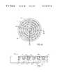
- FIG. 6is a top elevation view of an embodiment of a circular-polishing pad in accordance with the present invention.
- FIG. 7is a cross-sectional view along A 1 -A 2 of the pad of FIG. 6;
- FIGS. 8 and 9are top elevation views of exemplary portions of respective embodiments of linear polishing pads in accordance with the present invention.
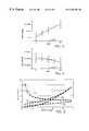
- FIGS. 10 and 11are graphs for removal rates of BPSG and TEOS, respectively, for an embodiment of a CMP process in accordance with the present invention.
- FIG. 12is a graph of duty cycle versus selectivity in accordance with the present invention.
- Substrate assembly 10comprises substrate 11 (e.g., a semiconductive material such as single crystalline silicon), transistor gate oxide 12 , transistor gate 13 , TEOS layer 14 , and BPSG layer 15 .
- substrate 11e.g., a semiconductive material such as single crystalline silicon
- transistor gate oxide 12transistor gate 13
- TEOS layer 14acts as an insulator for transistor gate 13 . As such, it is important not to remove too much TEOS from layer 14 when planarizing.
- FIG. 2there is shown a cross-sectional view of substrate assembly 10 of FIG. 1 after conventional planarization.
- TEOS layer 14has been completely remove above transistor gate 13 . This is to emphasize that owing to conventional selectivity limits, there is a relatively narrow process window in which to stop a CMP process from removing too much TEOS from layer 14 when planarizing BPSG layer 15 .
- FIG. 3there is shown a cross-sectional view of substrate assembly 10 after planarization in accordance with the present invention.
- a comparison of substrate assembly 10 of FIGS. 2 and 3demonstrates an increase in process window with the present invention.
- a CMP process windowis increased such that there is more time in which to expose substrate assembly 10 to polishing without significantly removing TEOS from layer 14 .
- FIG. 4there is shown a perspective view of an exemplary portion of a CMP system (chemical-mechanical polisher) 30 in accordance with the present invention.
- FIG. 5there is shown a cross-sectional view of CMP system 30 of FIG. 4, where drive assemblies 31 and 32 have been added.
- System 30comprises platen 21 , surface-patterned-non-porous polishing pad 22 , CMP solution 23 , support ring 24 , and substrate assembly carrier (“wafer carrier”) 25 .
- Wafer carriersubstrate assembly carrier
- Platen 21 and wafer carrier 25are attached to drive shafts 26 and 27 , respectively, for rotation.
- platen 21 and wafer carrier 25are rotated in a same direction, as illustratively indicated in FIG. 3 by arrows 28 and 29 .
- Other conventional details with respect to CMP system 30have been omitted to more clearly describe the present invention.
- wafer carrier 25may be rotated at one or more speeds, and such rotational speed may be varied during processing to affect material removal rate. It should be understood that it is not necessary to use rotational movement, rather any movement across contact portions and non-contact portions of pad 22 may be used, including but not limited to linear movement.
- Pad 22comprises a non-porous surface 43 having contact portions (e.g., islands) 41 and non-contact portions (e.g., recesses) 42 . While pad 22 may be made of a solid non-porous material, it may also be formed of more than one material, where a contact surface is formed of the non-porous material.
- pad 22has been shown with radially extending concentric islands and recesses, such configuration is just one embodiment.
- elliptical, spiral, or transverse (linear) recesses and islandsmay be employed in accordance with the present invention.
- discrete islandsmay be formed on a CMP pad.
- such discrete islandsmay be pillars, pyramids, mesas (including frusticonicals), cones, and like protrusions extending upward from a CMP pad surface.
- Such discrete islandsmay be spaced apart to provide at least one predetermined gap between them to provide at least one duty cycle.
- Such islandsmay be arranged to form rings, stripes, spirals, or ellipses, among other patterns.
- FIG. 7there is shown a cross-sectional view along A 1 -A 2 of pad 22 of FIG. 6 .
- Contact portions 41have formed or micro-roughened top surfaces 45 to allow CMP solution particles 50 to move across them.
- microelementssuch as those described in U.S. Pat. No. 5,578,362, may be impregnated in pad 22 to provide a micro-textured surface.
- Width (pitch) 44is wider than CMP solution particles 50 used in CMP solution 23 . While widths 44 are shown as uniform, widths of varying sizes may be used.
- pad 22is formed with contact and non-contact portions, as well as a non-porous surface 43 , it is possible to distinctly separate mechanical and chemical interactions of a CMP process. Therefore, such a CMP pad has both abrasion (contact to a substrate assembly surface with CMP solution particles) regions and hydrolyzation (contact to a substrate assembly surface with CMP solution) regions to remove material.
- material removalis mostly or completely a mechanical interaction governed by Preston's equation.
- non-contact portions 42material removal is mostly or completely a chemical interaction governed by the equation:
- R OHis the chemical removal rate
- K OHis a hydrolyzation reaction rate constant
- ⁇ [pH]is a function dependent on the pH level of CMP solution 23 .
- the amount of material removedis dependent in part upon the velocity, v, at which substrate assembly 40 is moved across non-contact portions 42 and contact portions 41 .
- a ratio of total material removed in a pass over L 1 and L 2may be mathematically expressed as: ( R OH , M1 * L 1 + R CMP , M1 * L 2 ) / v ( R OH , M2 * L 1 + R CMP , M2 * L 2 ) / v , ( 5 )
- R CMP,M1 and R CMP,M2are removal rates of non-hydrolyzed materials M 1 and M 2 , respectively.
- M 1is BPSG and M 2 is TEOS
- L 1is BPSG and M 2 is TEOS
- BPSG to TEOS selectivityis governed by the relative hydrolyzation rates of M 1 and M 2 .
- Such selectivitymay be approximated by an associated wet etch chemistry selectivity.
- CMP coefficientsi.e., the relative abrasion rates of M 1 and M 2
- approaches a non-recessed pad selectivityi.e., the relative abrasion rates of M 1 and M 2
- FIGS. 8 and 9illustratively show two non-porous pads 50 and 60 having different configurations in accordance with the present invention.
- Pad 50comprises transverse contact portions 51 and non-contact portions 52
- pad 60comprises transverse contact portions 61 and non-contact portions 62 .
- Pitch 54 of non-contact portions 52is greater than pitch 64 of non-contact portions 62 .
- Pads 50 and 60have different recess pitches, namely, pitch 54 and pitch 64 .
- pitches 54 and 64provide different contact frequencies. Consequently, contact-to-non-contact time ratio is adjustable. In other words, the ratio of contact portion 51 , 61 pitch to non-contact portion 52 , 62 pitch, respectively, affects contact-to-non-contact time.
- pad 50has a different non-contact to contact duty cycle than pad 60 . It should be understood that one or more predetermined duty cycles with respect to contact and non-contact portions may be provided with a pad in accordance with the present invention.
- FIGS. 10 and 11are graphs for removal rates of BPSG and TEOS, respectively, for the above-mentioned CMP process embodiment in accordance with the present invention.
- Contact portions of a CMP pad in accordance with the present inventionare directed to mechanical abrasion for material removal, and non-contact portions of the pad act as discrete reactors for chemical reaction, such as hydrolyzation of silicon oxide or oxidation of metal. Owing to forming such a pad with a non-porous surface having a predetermined duty cycle, chemical and mechanical actions to remove materials in a CMP process are separated. Such a predetermined spatial frequency or duty cycle may be provided for enhancing selectively for removing one material over another.
- Duty cycle in FIG. 12is the ratio of L 1 /(L 1 +L 2 ).
- selectivityis varied with a change in duty cycle for four examples.
- periodicity in FIG. 12was set at or about 2 mm (i.e., L 1 +L 2 was set equal to 2 mm).
- Curve 101represents an example where diffusion coefficients and abrasion coefficients (e.g. K CMP ) are relatively dominant factors in selectivity, such as when two dielectrics are present. More particularly, diffusion coefficient (D) is affected by doping.
- Ddiffusion coefficient
- BPSG with a 7% P and 3% B dopingwas selected as M 1
- PTEOS with no dopingwas selected as M 2 .
- Curve 102represents an example where abrasion coefficients and chemical removal rates (e.g., R OH ) are relatively dominant factors in selectivity, such as when two dielectrics are present.
- R OHchemical removal rates
- HDP oxidewas selected as M 1
- Si 3 N 4was selected as M 2 .
- Polishing a silicon nitride in the above examplemay be extrapolated to polishing a semiconductor, such as silicon, germanium, et al., or a semiconductive composition, such as a GaAs, et al., in the presence of a dielectric.
- a semiconductorsuch as silicon, germanium, et al.
- a semiconductive compositionsuch as a GaAs, et al.
- Curves 103 and 104represent examples where chemical removal rates, abrasion coefficients, and passivation efficiency (P) are relatively dominant factors in selectivity, such as when two dielectrics or two conductors are present.
- BPSGwas selected as M 1
- tungsten (W)was selected as M 2 .
- curve 104aluminum (Al) was selected as M 1 , and titanium (Ti) was selected as M 2 .
- the ratio of K CMP,M1 to K CMP,M2is about 10, and the ratio of R OH,M1 to R OH,M2 is about 0.5.
- a CMP padmay be configured to have a target selectivity with respect to removing one or more materials in the presence of one or more other materials. Such a pad may then be placed on a CMP platform (e.g., platen, web, belt, and the like) for more selectively removing one or more materials over one or more other materials from a substrate assembly.
- a CMP platforme.g., platen, web, belt, and the like
Landscapes
- Engineering & Computer Science (AREA)
- Mechanical Engineering (AREA)
- Mechanical Treatment Of Semiconductor (AREA)
- Finish Polishing, Edge Sharpening, And Grinding By Specific Grinding Devices (AREA)
Abstract
Description


Claims (20)
Priority Applications (3)
| Application Number | Priority Date | Filing Date | Title |
|---|---|---|---|
| US09/146,733US6203407B1 (en) | 1998-09-03 | 1998-09-03 | Method and apparatus for increasing-chemical-polishing selectivity |
| US09/800,711US6325702B2 (en) | 1998-09-03 | 2001-03-07 | Method and apparatus for increasing chemical-mechanical-polishing selectivity |
| US09/961,624US6893325B2 (en) | 1998-09-03 | 2001-09-24 | Method and apparatus for increasing chemical-mechanical-polishing selectivity |
Applications Claiming Priority (1)
| Application Number | Priority Date | Filing Date | Title |
|---|---|---|---|
| US09/146,733US6203407B1 (en) | 1998-09-03 | 1998-09-03 | Method and apparatus for increasing-chemical-polishing selectivity |
Related Child Applications (1)
| Application Number | Title | Priority Date | Filing Date |
|---|---|---|---|
| US09/800,711DivisionUS6325702B2 (en) | 1998-09-03 | 2001-03-07 | Method and apparatus for increasing chemical-mechanical-polishing selectivity |
Publications (1)
| Publication Number | Publication Date |
|---|---|
| US6203407B1true US6203407B1 (en) | 2001-03-20 |
Family
ID=22518760
Family Applications (3)
| Application Number | Title | Priority Date | Filing Date |
|---|---|---|---|
| US09/146,733Expired - LifetimeUS6203407B1 (en) | 1998-09-03 | 1998-09-03 | Method and apparatus for increasing-chemical-polishing selectivity |
| US09/800,711Expired - Fee RelatedUS6325702B2 (en) | 1998-09-03 | 2001-03-07 | Method and apparatus for increasing chemical-mechanical-polishing selectivity |
| US09/961,624Expired - Fee RelatedUS6893325B2 (en) | 1998-09-03 | 2001-09-24 | Method and apparatus for increasing chemical-mechanical-polishing selectivity |
Family Applications After (2)
| Application Number | Title | Priority Date | Filing Date |
|---|---|---|---|
| US09/800,711Expired - Fee RelatedUS6325702B2 (en) | 1998-09-03 | 2001-03-07 | Method and apparatus for increasing chemical-mechanical-polishing selectivity |
| US09/961,624Expired - Fee RelatedUS6893325B2 (en) | 1998-09-03 | 2001-09-24 | Method and apparatus for increasing chemical-mechanical-polishing selectivity |
Country Status (1)
| Country | Link |
|---|---|
| US (3) | US6203407B1 (en) |
Cited By (49)
| Publication number | Priority date | Publication date | Assignee | Title |
|---|---|---|---|---|
| US6287174B1 (en)* | 1999-02-05 | 2001-09-11 | Rodel Holdings Inc. | Polishing pad and method of use thereof |
| US20020069967A1 (en)* | 2000-05-04 | 2002-06-13 | Wright David Q. | Planarizing machines and methods for mechanical and/or chemical-mechanical planarization of microelectronic-device substrate assemblies |
| US20020072302A1 (en)* | 1998-09-03 | 2002-06-13 | Micron Technology, Inc. | Method and apparatus for increasing chemical-mechanical-polishing selectivity |
| US6498101B1 (en) | 2000-02-28 | 2002-12-24 | Micron Technology, Inc. | Planarizing pads, planarizing machines and methods for making and using planarizing pads in mechanical and chemical-mechanical planarization of microelectronic device substrate assemblies |
| US6511576B2 (en) | 1999-11-17 | 2003-01-28 | Micron Technology, Inc. | System for planarizing microelectronic substrates having apertures |
| US6520834B1 (en) | 2000-08-09 | 2003-02-18 | Micron Technology, Inc. | Methods and apparatuses for analyzing and controlling performance parameters in mechanical and chemical-mechanical planarization of microelectronic substrates |
| US6520847B2 (en)* | 1997-05-15 | 2003-02-18 | Applied Materials, Inc. | Polishing pad having a grooved pattern for use in chemical mechanical polishing |
| US6530829B1 (en) | 2001-08-30 | 2003-03-11 | Micron Technology, Inc. | CMP pad having isolated pockets of continuous porosity and a method for using such pad |
| US6533893B2 (en) | 1999-09-02 | 2003-03-18 | Micron Technology, Inc. | Method and apparatus for chemical-mechanical planarization of microelectronic substrates with selected planarizing liquids |
| US6548407B1 (en) | 2000-04-26 | 2003-04-15 | Micron Technology, Inc. | Method and apparatus for controlling chemical interactions during planarization of microelectronic substrates |
| US6592443B1 (en) | 2000-08-30 | 2003-07-15 | Micron Technology, Inc. | Method and apparatus for forming and using planarizing pads for mechanical and chemical-mechanical planarization of microelectronic substrates |
| US6607423B1 (en)* | 1999-03-03 | 2003-08-19 | Advanced Micro Devices, Inc. | Method for achieving a desired semiconductor wafer surface profile via selective polishing pad conditioning |
| US6623329B1 (en) | 2000-08-31 | 2003-09-23 | Micron Technology, Inc. | Method and apparatus for supporting a microelectronic substrate relative to a planarization pad |
| US6628410B2 (en) | 1996-02-16 | 2003-09-30 | Micron Technology, Inc. | Endpoint detector and method for measuring a change in wafer thickness in chemical-mechanical polishing of semiconductor wafers and other microelectronic substrates |
| US20030194959A1 (en)* | 2002-04-15 | 2003-10-16 | Cabot Microelectronics Corporation | Sintered polishing pad with regions of contrasting density |
| US6652764B1 (en) | 2000-08-31 | 2003-11-25 | Micron Technology, Inc. | Methods and apparatuses for making and using planarizing pads for mechanical and chemical-mechanical planarization of microelectronic substrates |
| US6666749B2 (en) | 2001-08-30 | 2003-12-23 | Micron Technology, Inc. | Apparatus and method for enhanced processing of microelectronic workpieces |
| US20040012795A1 (en)* | 2000-08-30 | 2004-01-22 | Moore Scott E. | Planarizing machines and control systems for mechanical and/or chemical-mechanical planarization of microelectronic substrates |
| US20040038623A1 (en)* | 2002-08-26 | 2004-02-26 | Nagasubramaniyan Chandrasekaran | Methods and systems for conditioning planarizing pads used in planarizing substrates |
| US6736869B1 (en) | 2000-08-28 | 2004-05-18 | Micron Technology, Inc. | Method for forming a planarizing pad for planarization of microelectronic substrates |
| US20040198184A1 (en)* | 2001-08-24 | 2004-10-07 | Joslyn Michael J | Planarizing machines and methods for dispensing planarizing solutions in the processing of microelectronic workpieces |
| US20040214509A1 (en)* | 2003-04-28 | 2004-10-28 | Elledge Jason B. | Systems and methods for mechanical and/or chemical-mechanical polishing of microfeature workpieces |
| US6838382B1 (en) | 2000-08-28 | 2005-01-04 | Micron Technology, Inc. | Method and apparatus for forming a planarizing pad having a film and texture elements for planarization of microelectronic substrates |
| US20050014457A1 (en)* | 2001-08-24 | 2005-01-20 | Taylor Theodore M. | Apparatus and method for conditioning a contact surface of a processing pad used in processing microelectronic workpieces |
| US20050020191A1 (en)* | 2002-03-04 | 2005-01-27 | Taylor Theodore M. | Apparatus for planarizing microelectronic workpieces |
| US20050026544A1 (en)* | 2003-01-16 | 2005-02-03 | Elledge Jason B. | Carrier assemblies, polishing machines including carrier assemblies, and methods for polishing micro-device workpieces |
| US20050040813A1 (en)* | 2003-08-21 | 2005-02-24 | Suresh Ramarajan | Apparatuses and methods for monitoring rotation of a conductive microfeature workpiece |
| US20050064797A1 (en)* | 2003-09-18 | 2005-03-24 | Taylor Theodore M. | Methods for removing doped silicon material from microfeature workpieces |
| US6884152B2 (en) | 2003-02-11 | 2005-04-26 | Micron Technology, Inc. | Apparatuses and methods for conditioning polishing pads used in polishing micro-device workpieces |
| US20050090105A1 (en)* | 2002-07-18 | 2005-04-28 | Micron Technology, Inc. | Methods and systems for planarizing workpieces, e.g., Microelectronic workpieces |
| US20050118930A1 (en)* | 2002-08-23 | 2005-06-02 | Nagasubramaniyan Chandrasekaran | Carrier assemblies, planarizing apparatuses including carrier assemblies, and methods for planarizing micro-device workpieces |
| US20050153634A1 (en)* | 2004-01-09 | 2005-07-14 | Cabot Microelectronics Corporation | Negative poisson's ratio material-containing CMP polishing pad |
| US6935929B2 (en) | 2003-04-28 | 2005-08-30 | Micron Technology, Inc. | Polishing machines including under-pads and methods for mechanical and/or chemical-mechanical polishing of microfeature workpieces |
| US20050202756A1 (en)* | 2004-03-09 | 2005-09-15 | Carter Moore | Methods and systems for planarizing workpieces, e.g., microelectronic workpieces |
| US20050266773A1 (en)* | 2000-06-07 | 2005-12-01 | Micron Technology, Inc. | Apparatuses and methods for in-situ optical endpointing on web-format planarizing machines in mechanical or chemical-mechanical planarization of microelectronic-device substrate assemblies |
| US20060030242A1 (en)* | 2004-08-06 | 2006-02-09 | Taylor Theodore M | Shaped polishing pads for beveling microfeature workpiece edges, and associate system and methods |
| KR20060045167A (en)* | 2004-11-09 | 2006-05-17 | 동성에이앤티 주식회사 | Polishing pads and manufacturing method thereof |
| US20070049177A1 (en)* | 2005-09-01 | 2007-03-01 | Micron Technology, Inc. | Method and apparatus for removing material from microfeature workpieces |
| US20070049172A1 (en)* | 2005-08-31 | 2007-03-01 | Micron Technology, Inc. | Apparatus and method for removing material from microfeature workpieces |
| US20070161332A1 (en)* | 2005-07-13 | 2007-07-12 | Micron Technology, Inc. | Systems and methods for removing microfeature workpiece surface defects |
| US20090318067A1 (en)* | 2008-06-19 | 2009-12-24 | Allen Chiu | Polishing pad and the method of forming micro-structure thereof |
| US20100056031A1 (en)* | 2008-08-29 | 2010-03-04 | Allen Chiu | Polishing Pad |
| US20100105303A1 (en)* | 2008-10-23 | 2010-04-29 | Allen Chiu | Polishing Pad |
| US20140326701A1 (en)* | 2011-12-21 | 2014-11-06 | Basf Se | Process for the manufacture of semiconductor devices comprising the chemical mechanical polishing of borophosphosilicate glass (bpsg) material in the presence of a cmp composition comprising anionic phosphate or phosphonate |
| US20160375546A1 (en)* | 2015-06-29 | 2016-12-29 | Iv Technologies Co., Ltd. | Polishing layer of polishing pad and method of forming the same and polishing method |
| US20170028526A1 (en)* | 2015-07-30 | 2017-02-02 | Jh Rhodes Company, Inc. | Polymeric lapping materials, media and systems including polymeric lapping material, and methods of forming and using same |
| US20180161953A1 (en)* | 2016-12-14 | 2018-06-14 | Taiwan Semiconductor Manufacturing Company, Ltd. | Polishing pad and method of using |
| WO2018116122A1 (en)* | 2016-12-21 | 2018-06-28 | 3M Innovative Properties Company | Pad conditioner with spacer and wafer planarization system |
| US10562149B2 (en) | 2015-09-25 | 2020-02-18 | Cabot Microelectronics Corporation | Polyurethane CMP pads having a high modulus ratio |
Families Citing this family (24)
| Publication number | Priority date | Publication date | Assignee | Title |
|---|---|---|---|---|
| US6869343B2 (en)* | 2001-12-19 | 2005-03-22 | Toho Engineering Kabushiki Kaisha | Turning tool for grooving polishing pad, apparatus and method of producing polishing pad using the tool, and polishing pad produced by using the tool |
| US7516536B2 (en)* | 1999-07-08 | 2009-04-14 | Toho Engineering Kabushiki Kaisha | Method of producing polishing pad |
| AU1274401A (en)* | 1999-10-21 | 2001-04-30 | Technolas Gmbh Ophthalmologische Systeme | Multi-step laser correction of ophthalmic refractive errors |
| US6943114B2 (en)* | 2002-02-28 | 2005-09-13 | Infineon Technologies Ag | Integration scheme for metal gap fill, with fixed abrasive CMP |
| US6641632B1 (en)* | 2002-11-18 | 2003-11-04 | International Business Machines Corporation | Polishing compositions and use thereof |
| US6866560B1 (en)* | 2003-01-09 | 2005-03-15 | Sandia Corporation | Method for thinning specimen |
| US7160178B2 (en)* | 2003-08-07 | 2007-01-09 | 3M Innovative Properties Company | In situ activation of a three-dimensional fixed abrasive article |
| US20050042976A1 (en)* | 2003-08-22 | 2005-02-24 | International Business Machines Corporation | Low friction planarizing/polishing pads and use thereof |
| TWI238100B (en)* | 2003-09-29 | 2005-08-21 | Iv Technologies Co Ltd | Polishing pad and fabricating method thereof |
| US7449067B2 (en)* | 2003-11-03 | 2008-11-11 | International Business Machines Corporation | Method and apparatus for filling vias |
| US6951509B1 (en)* | 2004-03-09 | 2005-10-04 | 3M Innovative Properties Company | Undulated pad conditioner and method of using same |
| US20060079159A1 (en)* | 2004-10-08 | 2006-04-13 | Markus Naujok | Chemical mechanical polish with multi-zone abrasive-containing matrix |
| DE102005053297A1 (en)* | 2005-11-08 | 2007-05-10 | Bausch & Lomb Inc. | System and method for correcting ophthalmic refractive errors |
| DE102006036085A1 (en)* | 2006-08-02 | 2008-02-07 | Bausch & Lomb Incorporated | Method and apparatus for calculating a laser shot file for use in an excimer laser |
| DE102006036086A1 (en)* | 2006-08-02 | 2008-02-07 | Bausch & Lomb Incorporated | Method and apparatus for calculating a laser shot file for use in a refractive excimer laser |
| US20080271384A1 (en)* | 2006-09-22 | 2008-11-06 | Saint-Gobain Ceramics & Plastics, Inc. | Conditioning tools and techniques for chemical mechanical planarization |
| ITMC20070237A1 (en)* | 2007-12-12 | 2009-06-13 | Ghines Srl | PERFECTED ABRASIVE TOOL. |
| DE102008028509A1 (en)* | 2008-06-16 | 2009-12-24 | Technolas Gmbh Ophthalmologische Systeme | Treatment pattern monitoring device |
| DE102008035995A1 (en)* | 2008-08-01 | 2010-02-04 | Technolas Perfect Vision Gmbh | Combination of excimer laser ablation and femtosecond laser technique |
| CN102137617A (en)* | 2008-08-28 | 2011-07-27 | 泰克诺拉斯完美视觉股份有限公司 | Eye measurement and modeling techniques |
| KR101413030B1 (en)* | 2009-03-24 | 2014-07-02 | 생-고벵 아브라시프 | Abrasive tool for use as a chemical mechanical planarization pad conditioner |
| US8905823B2 (en)* | 2009-06-02 | 2014-12-09 | Saint-Gobain Abrasives, Inc. | Corrosion-resistant CMP conditioning tools and methods for making and using same |
| US20110097977A1 (en)* | 2009-08-07 | 2011-04-28 | Abrasive Technology, Inc. | Multiple-sided cmp pad conditioning disk |
| WO2011028700A2 (en) | 2009-09-01 | 2011-03-10 | Saint-Gobain Abrasives, Inc. | Chemical mechanical polishing conditioner |
Citations (87)
| Publication number | Priority date | Publication date | Assignee | Title |
|---|---|---|---|---|
| US816461A (en) | 1904-12-22 | 1906-03-27 | George Gorton | Clearance-space grinding-disk. |
| GB190626287A (en) | 1906-11-20 | 1907-11-20 | William Oliver Bailey | Improvements in Mills for Grinding and Polishing Glass. |
| US888129A (en) | 1905-04-25 | 1908-05-19 | Carborundum Co | Manufacture of abrasive material. |
| US959054A (en) | 1909-03-08 | 1910-05-24 | Charles Glover | Grinding and polishing disk. |
| US1953983A (en) | 1928-02-07 | 1934-04-10 | Carborundum Co | Manufacture of rubber bonded abrasive articles |
| US2242877A (en) | 1939-03-15 | 1941-05-20 | Albertson & Co Inc | Abrasive disk and method of making the same |
| US2409953A (en) | 1943-10-13 | 1946-10-22 | Western Electric Co | Material treating apparatus |
| US2653428A (en) | 1952-04-10 | 1953-09-29 | Paul K Fuller | Grinding disk |
| US2749681A (en) | 1952-12-31 | 1956-06-12 | Stephen U Sohne A | Grinding disc |
| US2749683A (en) | 1954-10-05 | 1956-06-12 | Western Electric Co | Lapping plate |
| FR1195595A (en) | 1958-05-05 | 1959-11-18 | Improvements to grindstones, especially for stonework | |
| CA679731A (en) | 1964-02-11 | H. Sandmeyer Karl | Bonded abrasive articles | |
| US3468079A (en) | 1966-09-21 | 1969-09-23 | Kaufman Jack W | Abrasive-like tool device |
| US3495362A (en) | 1967-03-17 | 1970-02-17 | Thunderbird Abrasives Inc | Abrasive disk |
| US3517466A (en) | 1969-07-18 | 1970-06-30 | Ferro Corp | Stone polishing wheel for contoured surfaces |
| FR2063961A1 (en) | 1969-10-13 | 1971-07-16 | Radiotechnique Compelec | Mechanico-chemical grinder for semi-con-ducting panels |
| US3627338A (en)* | 1969-10-09 | 1971-12-14 | Sheldon Thompson | Vacuum chuck |
| US4183545A (en)* | 1978-07-28 | 1980-01-15 | Advanced Simiconductor Materials/America | Rotary vacuum-chuck using no rotary union |
| GB2043501A (en) | 1979-02-28 | 1980-10-08 | Interface Developments Ltd | Abrading member |
| US4244775A (en) | 1979-04-30 | 1981-01-13 | Bell Telephone Laboratories, Incorporated | Process for the chemical etch polishing of semiconductors |
| US4271640A (en) | 1978-02-17 | 1981-06-09 | Minnesota Mining And Manufacturing Company | Rotatable floor treating pad |
| USRE31053E (en) | 1978-01-23 | 1982-10-12 | Bell Telephone Laboratories, Incorporated | Apparatus and method for holding and planarizing thin workpieces |
| US4373991A (en) | 1982-01-28 | 1983-02-15 | Western Electric Company, Inc. | Methods and apparatus for polishing a semiconductor wafer |
| SU1206067A1 (en) | 1984-02-14 | 1986-01-23 | Научно-Исследовательский Институт "Сапфир" | Tool for hydrodynamic working of flat articles |
| US4603867A (en)* | 1984-04-02 | 1986-08-05 | Motorola, Inc. | Spinner chuck |
| US4621458A (en) | 1985-10-08 | 1986-11-11 | Smith Robert S | Flat disk polishing apparatus |
| JPS6299072A (en) | 1985-10-22 | 1987-05-08 | Sumitomo Electric Ind Ltd | Semiconductor wafer processing method |
| US4663890A (en) | 1982-05-18 | 1987-05-12 | Gmn Georg Muller Nurnberg Gmbh | Method for machining workpieces of brittle hard material into wafers |
| US4666553A (en) | 1985-08-28 | 1987-05-19 | Rca Corporation | Method for planarizing multilayer semiconductor devices |
| US4671851A (en) | 1985-10-28 | 1987-06-09 | International Business Machines Corporation | Method for removing protuberances at the surface of a semiconductor wafer using a chem-mech polishing technique |
| US4679359A (en) | 1984-12-28 | 1987-07-14 | Fuji Seiki Machine Works, Ltd. | Method for preparation of silicon wafer |
| US4693036A (en) | 1983-12-28 | 1987-09-15 | Disco Abrasive Systems, Ltd. | Semiconductor wafer surface grinding apparatus |
| US4711610A (en)* | 1986-04-04 | 1987-12-08 | Machine Technology, Inc. | Balancing chuck |
| US4715150A (en) | 1986-04-29 | 1987-12-29 | Seiken Co., Ltd. | Nonwoven fiber abrasive disk |
| US4739589A (en) | 1985-07-12 | 1988-04-26 | Wacker-Chemitronic Gesellschaft Fur Elektronik-Grundstoff Mbh | Process and apparatus for abrasive machining of a wafer-like workpiece |
| US4773185A (en) | 1986-01-31 | 1988-09-27 | Linden Integral Research, Inc. | Surface abrading machine |
| US4789424A (en) | 1987-12-11 | 1988-12-06 | Frank Fornadel | Apparatus and process for optic polishing |
| US4811522A (en) | 1987-03-23 | 1989-03-14 | Gill Jr Gerald L | Counterbalanced polishing apparatus |
| US4821461A (en) | 1987-11-23 | 1989-04-18 | Magnetic Peripherals Inc. | Textured lapping plate and process for its manufacture |
| US4843766A (en) | 1985-11-05 | 1989-07-04 | Disco Abrasive Systems, Ltd. | Cutting tool having concentrically arranged outside and inside abrasive grain layers and method for production thereof |
| US4918872A (en) | 1984-05-14 | 1990-04-24 | Kanebo Limited | Surface grinding apparatus |
| US5020283A (en) | 1990-01-22 | 1991-06-04 | Micron Technology, Inc. | Polishing pad with uniform abrasion |
| US5036015A (en) | 1990-09-24 | 1991-07-30 | Micron Technology, Inc. | Method of endpoint detection during chemical/mechanical planarization of semiconductor wafers |
| US5069002A (en) | 1991-04-17 | 1991-12-03 | Micron Technology, Inc. | Apparatus for endpoint detection during mechanical planarization of semiconductor wafers |
| US5081796A (en) | 1990-08-06 | 1992-01-21 | Micron Technology, Inc. | Method and apparatus for mechanical planarization and endpoint detection of a semiconductor wafer |
| US5131190A (en) | 1990-02-23 | 1992-07-21 | C.I.C.E. S.A. | Lapping machine and non-constant pitch grooved bed therefor |
| US5137597A (en) | 1991-04-11 | 1992-08-11 | Microelectronics And Computer Technology Corporation | Fabrication of metal pillars in an electronic component using polishing |
| US5142828A (en) | 1990-06-25 | 1992-09-01 | Microelectronics And Computer Technology Corporation | Correcting a defective metallization layer on an electronic component by polishing |
| US5169491A (en) | 1991-07-29 | 1992-12-08 | Micron Technology, Inc. | Method of etching SiO2 dielectric layers using chemical mechanical polishing techniques |
| US5177908A (en) | 1990-01-22 | 1993-01-12 | Micron Technology, Inc. | Polishing pad |
| US5196353A (en) | 1992-01-03 | 1993-03-23 | Micron Technology, Inc. | Method for controlling a semiconductor (CMP) process by measuring a surface temperature and developing a thermal image of the wafer |
| US5209816A (en) | 1992-06-04 | 1993-05-11 | Micron Technology, Inc. | Method of chemical mechanical polishing aluminum containing metal layers and slurry for chemical mechanical polishing |
| US5216843A (en) | 1992-09-24 | 1993-06-08 | Intel Corporation | Polishing pad conditioning apparatus for wafer planarization process |
| US5223734A (en) | 1991-12-18 | 1993-06-29 | Micron Technology, Inc. | Semiconductor gettering process using backside chemical mechanical planarization (CMP) and dopant diffusion |
| US5222329A (en) | 1992-03-26 | 1993-06-29 | Micron Technology, Inc. | Acoustical method and system for detecting and controlling chemical-mechanical polishing (CMP) depths into layers of conductors, semiconductors, and dielectric materials |
| US5225034A (en) | 1992-06-04 | 1993-07-06 | Micron Technology, Inc. | Method of chemical mechanical polishing predominantly copper containing metal layers in semiconductor processing |
| US5232875A (en) | 1992-10-15 | 1993-08-03 | Micron Technology, Inc. | Method and apparatus for improving planarity of chemical-mechanical planarization operations |
| US5234867A (en) | 1992-05-27 | 1993-08-10 | Micron Technology, Inc. | Method for planarizing semiconductor wafers with a non-circular polishing pad |
| US5240552A (en) | 1991-12-11 | 1993-08-31 | Micron Technology, Inc. | Chemical mechanical planarization (CMP) of a semiconductor wafer using acoustical waves for in-situ end point detection |
| US5244534A (en) | 1992-01-24 | 1993-09-14 | Micron Technology, Inc. | Two-step chemical mechanical polishing process for producing flush and protruding tungsten plugs |
| USRE34425E (en) | 1990-08-06 | 1993-11-02 | Micron Technology, Inc. | Method and apparatus for mechanical planarization and endpoint detection of a semiconductor wafer |
| US5300155A (en) | 1992-12-23 | 1994-04-05 | Micron Semiconductor, Inc. | IC chemical mechanical planarization process incorporating slurry temperature control |
| US5302233A (en) | 1993-03-19 | 1994-04-12 | Micron Semiconductor, Inc. | Method for shaping features of a semiconductor structure using chemical mechanical planarization (CMP) |
| US5314843A (en) | 1992-03-27 | 1994-05-24 | Micron Technology, Inc. | Integrated circuit polishing method |
| US5318927A (en) | 1993-04-29 | 1994-06-07 | Micron Semiconductor, Inc. | Methods of chemical-mechanical polishing insulating inorganic metal oxide materials |
| US5329734A (en) | 1993-04-30 | 1994-07-19 | Motorola, Inc. | Polishing pads used to chemical-mechanical polish a semiconductor substrate |
| US5380546A (en) | 1993-06-09 | 1995-01-10 | Microelectronics And Computer Technology Corporation | Multilevel metallization process for electronic components |
| US5382551A (en) | 1993-04-09 | 1995-01-17 | Micron Semiconductor, Inc. | Method for reducing the effects of semiconductor substrate deformities |
| US5394655A (en) | 1993-08-31 | 1995-03-07 | Texas Instruments Incorporated | Semiconductor polishing pad |
| US5395801A (en) | 1993-09-29 | 1995-03-07 | Micron Semiconductor, Inc. | Chemical-mechanical polishing processes of planarizing insulating layers |
| US5413941A (en) | 1994-01-06 | 1995-05-09 | Micron Technology, Inc. | Optical end point detection methods in semiconductor planarizing polishing processes |
| US5439551A (en) | 1994-03-02 | 1995-08-08 | Micron Technology, Inc. | Chemical-mechanical polishing techniques and methods of end point detection in chemical-mechanical polishing processes |
| US5441598A (en) | 1993-12-16 | 1995-08-15 | Motorola, Inc. | Polishing pad for chemical-mechanical polishing of a semiconductor substrate |
| US5449314A (en) | 1994-04-25 | 1995-09-12 | Micron Technology, Inc. | Method of chimical mechanical polishing for dielectric layers |
| US5486129A (en) | 1993-08-25 | 1996-01-23 | Micron Technology, Inc. | System and method for real-time control of semiconductor a wafer polishing, and a polishing head |
| US5487697A (en) | 1993-02-09 | 1996-01-30 | Rodel, Inc. | Polishing apparatus and method using a rotary work holder travelling down a rail for polishing a workpiece with linear pads |
| US5489233A (en) | 1994-04-08 | 1996-02-06 | Rodel, Inc. | Polishing pads and methods for their use |
| US5514245A (en) | 1992-01-27 | 1996-05-07 | Micron Technology, Inc. | Method for chemical planarization (CMP) of a semiconductor wafer to provide a planar surface free of microscratches |
| US5533924A (en) | 1994-09-01 | 1996-07-09 | Micron Technology, Inc. | Polishing apparatus, a polishing wafer carrier apparatus, a replacable component for a particular polishing apparatus and a process of polishing wafers |
| US5540810A (en) | 1992-12-11 | 1996-07-30 | Micron Technology Inc. | IC mechanical planarization process incorporating two slurry compositions for faster material removal times |
| US5558563A (en) | 1995-02-23 | 1996-09-24 | International Business Machines Corporation | Method and apparatus for uniform polishing of a substrate |
| US5578362A (en) | 1992-08-19 | 1996-11-26 | Rodel, Inc. | Polymeric polishing pad containing hollow polymeric microelements |
| US5605760A (en) | 1995-08-21 | 1997-02-25 | Rodel, Inc. | Polishing pads |
| US5609718A (en) | 1995-09-29 | 1997-03-11 | Micron Technology, Inc. | Method and apparatus for measuring a change in the thickness of polishing pads used in chemical-mechanical planarization of semiconductor wafers |
| US5650039A (en) | 1994-03-02 | 1997-07-22 | Applied Materials, Inc. | Chemical mechanical polishing apparatus with improved slurry distribution |
| US5690540A (en) | 1996-02-23 | 1997-11-25 | Micron Technology, Inc. | Spiral grooved polishing pad for chemical-mechanical planarization of semiconductor wafers |
| US5730642A (en)* | 1993-08-25 | 1998-03-24 | Micron Technology, Inc. | System for real-time control of semiconductor wafer polishing including optical montoring |
Family Cites Families (3)
| Publication number | Priority date | Publication date | Assignee | Title |
|---|---|---|---|---|
| US5441589A (en) | 1993-06-17 | 1995-08-15 | Taurus Impressions, Inc. | Flat bed daisy wheel hot debossing stamper |
| US5921855A (en)* | 1997-05-15 | 1999-07-13 | Applied Materials, Inc. | Polishing pad having a grooved pattern for use in a chemical mechanical polishing system |
| US6203407B1 (en)* | 1998-09-03 | 2001-03-20 | Micron Technology, Inc. | Method and apparatus for increasing-chemical-polishing selectivity |
- 1998
- 1998-09-03USUS09/146,733patent/US6203407B1/ennot_activeExpired - Lifetime
- 2001
- 2001-03-07USUS09/800,711patent/US6325702B2/ennot_activeExpired - Fee Related
- 2001-09-24USUS09/961,624patent/US6893325B2/ennot_activeExpired - Fee Related
Patent Citations (92)
| Publication number | Priority date | Publication date | Assignee | Title |
|---|---|---|---|---|
| CA679731A (en) | 1964-02-11 | H. Sandmeyer Karl | Bonded abrasive articles | |
| US816461A (en) | 1904-12-22 | 1906-03-27 | George Gorton | Clearance-space grinding-disk. |
| US888129A (en) | 1905-04-25 | 1908-05-19 | Carborundum Co | Manufacture of abrasive material. |
| GB190626287A (en) | 1906-11-20 | 1907-11-20 | William Oliver Bailey | Improvements in Mills for Grinding and Polishing Glass. |
| US959054A (en) | 1909-03-08 | 1910-05-24 | Charles Glover | Grinding and polishing disk. |
| US1953983A (en) | 1928-02-07 | 1934-04-10 | Carborundum Co | Manufacture of rubber bonded abrasive articles |
| US2242877A (en) | 1939-03-15 | 1941-05-20 | Albertson & Co Inc | Abrasive disk and method of making the same |
| US2409953A (en) | 1943-10-13 | 1946-10-22 | Western Electric Co | Material treating apparatus |
| US2653428A (en) | 1952-04-10 | 1953-09-29 | Paul K Fuller | Grinding disk |
| US2749681A (en) | 1952-12-31 | 1956-06-12 | Stephen U Sohne A | Grinding disc |
| US2749683A (en) | 1954-10-05 | 1956-06-12 | Western Electric Co | Lapping plate |
| FR1195595A (en) | 1958-05-05 | 1959-11-18 | Improvements to grindstones, especially for stonework | |
| US3468079A (en) | 1966-09-21 | 1969-09-23 | Kaufman Jack W | Abrasive-like tool device |
| US3495362A (en) | 1967-03-17 | 1970-02-17 | Thunderbird Abrasives Inc | Abrasive disk |
| US3517466A (en) | 1969-07-18 | 1970-06-30 | Ferro Corp | Stone polishing wheel for contoured surfaces |
| US3627338A (en)* | 1969-10-09 | 1971-12-14 | Sheldon Thompson | Vacuum chuck |
| FR2063961A1 (en) | 1969-10-13 | 1971-07-16 | Radiotechnique Compelec | Mechanico-chemical grinder for semi-con-ducting panels |
| USRE31053E (en) | 1978-01-23 | 1982-10-12 | Bell Telephone Laboratories, Incorporated | Apparatus and method for holding and planarizing thin workpieces |
| US4271640A (en) | 1978-02-17 | 1981-06-09 | Minnesota Mining And Manufacturing Company | Rotatable floor treating pad |
| US4183545A (en)* | 1978-07-28 | 1980-01-15 | Advanced Simiconductor Materials/America | Rotary vacuum-chuck using no rotary union |
| GB2043501A (en) | 1979-02-28 | 1980-10-08 | Interface Developments Ltd | Abrading member |
| US4244775A (en) | 1979-04-30 | 1981-01-13 | Bell Telephone Laboratories, Incorporated | Process for the chemical etch polishing of semiconductors |
| US4373991A (en) | 1982-01-28 | 1983-02-15 | Western Electric Company, Inc. | Methods and apparatus for polishing a semiconductor wafer |
| US4663890A (en) | 1982-05-18 | 1987-05-12 | Gmn Georg Muller Nurnberg Gmbh | Method for machining workpieces of brittle hard material into wafers |
| US4693036A (en) | 1983-12-28 | 1987-09-15 | Disco Abrasive Systems, Ltd. | Semiconductor wafer surface grinding apparatus |
| SU1206067A1 (en) | 1984-02-14 | 1986-01-23 | Научно-Исследовательский Институт "Сапфир" | Tool for hydrodynamic working of flat articles |
| US4603867A (en)* | 1984-04-02 | 1986-08-05 | Motorola, Inc. | Spinner chuck |
| US4918872A (en) | 1984-05-14 | 1990-04-24 | Kanebo Limited | Surface grinding apparatus |
| US4679359A (en) | 1984-12-28 | 1987-07-14 | Fuji Seiki Machine Works, Ltd. | Method for preparation of silicon wafer |
| US4739589A (en) | 1985-07-12 | 1988-04-26 | Wacker-Chemitronic Gesellschaft Fur Elektronik-Grundstoff Mbh | Process and apparatus for abrasive machining of a wafer-like workpiece |
| US4666553A (en) | 1985-08-28 | 1987-05-19 | Rca Corporation | Method for planarizing multilayer semiconductor devices |
| US4621458A (en) | 1985-10-08 | 1986-11-11 | Smith Robert S | Flat disk polishing apparatus |
| JPS6299072A (en) | 1985-10-22 | 1987-05-08 | Sumitomo Electric Ind Ltd | Semiconductor wafer processing method |
| US4671851A (en) | 1985-10-28 | 1987-06-09 | International Business Machines Corporation | Method for removing protuberances at the surface of a semiconductor wafer using a chem-mech polishing technique |
| US4843766A (en) | 1985-11-05 | 1989-07-04 | Disco Abrasive Systems, Ltd. | Cutting tool having concentrically arranged outside and inside abrasive grain layers and method for production thereof |
| US4773185A (en) | 1986-01-31 | 1988-09-27 | Linden Integral Research, Inc. | Surface abrading machine |
| US4711610A (en)* | 1986-04-04 | 1987-12-08 | Machine Technology, Inc. | Balancing chuck |
| US4715150A (en) | 1986-04-29 | 1987-12-29 | Seiken Co., Ltd. | Nonwoven fiber abrasive disk |
| US4811522A (en) | 1987-03-23 | 1989-03-14 | Gill Jr Gerald L | Counterbalanced polishing apparatus |
| EP0318135A2 (en) | 1987-11-23 | 1989-05-31 | Magnetic Peripherals Inc. | Abrading tool and process of manufacturing the same |
| US4821461A (en) | 1987-11-23 | 1989-04-18 | Magnetic Peripherals Inc. | Textured lapping plate and process for its manufacture |
| US4789424A (en) | 1987-12-11 | 1988-12-06 | Frank Fornadel | Apparatus and process for optic polishing |
| US5020283A (en) | 1990-01-22 | 1991-06-04 | Micron Technology, Inc. | Polishing pad with uniform abrasion |
| US5421769A (en) | 1990-01-22 | 1995-06-06 | Micron Technology, Inc. | Apparatus for planarizing semiconductor wafers, and a polishing pad for a planarization apparatus |
| EP0439124A2 (en) | 1990-01-22 | 1991-07-31 | Micron Technology, Inc. | Polishing pad with uniform abrasion |
| US5297364A (en) | 1990-01-22 | 1994-03-29 | Micron Technology, Inc. | Polishing pad with controlled abrasion rate |
| US5177908A (en) | 1990-01-22 | 1993-01-12 | Micron Technology, Inc. | Polishing pad |
| US5131190A (en) | 1990-02-23 | 1992-07-21 | C.I.C.E. S.A. | Lapping machine and non-constant pitch grooved bed therefor |
| US5142828A (en) | 1990-06-25 | 1992-09-01 | Microelectronics And Computer Technology Corporation | Correcting a defective metallization layer on an electronic component by polishing |
| US5081796A (en) | 1990-08-06 | 1992-01-21 | Micron Technology, Inc. | Method and apparatus for mechanical planarization and endpoint detection of a semiconductor wafer |
| USRE34425E (en) | 1990-08-06 | 1993-11-02 | Micron Technology, Inc. | Method and apparatus for mechanical planarization and endpoint detection of a semiconductor wafer |
| US5036015A (en) | 1990-09-24 | 1991-07-30 | Micron Technology, Inc. | Method of endpoint detection during chemical/mechanical planarization of semiconductor wafers |
| US5137597A (en) | 1991-04-11 | 1992-08-11 | Microelectronics And Computer Technology Corporation | Fabrication of metal pillars in an electronic component using polishing |
| US5069002A (en) | 1991-04-17 | 1991-12-03 | Micron Technology, Inc. | Apparatus for endpoint detection during mechanical planarization of semiconductor wafers |
| US5169491A (en) | 1991-07-29 | 1992-12-08 | Micron Technology, Inc. | Method of etching SiO2 dielectric layers using chemical mechanical polishing techniques |
| US5240552A (en) | 1991-12-11 | 1993-08-31 | Micron Technology, Inc. | Chemical mechanical planarization (CMP) of a semiconductor wafer using acoustical waves for in-situ end point detection |
| US5223734A (en) | 1991-12-18 | 1993-06-29 | Micron Technology, Inc. | Semiconductor gettering process using backside chemical mechanical planarization (CMP) and dopant diffusion |
| US5196353A (en) | 1992-01-03 | 1993-03-23 | Micron Technology, Inc. | Method for controlling a semiconductor (CMP) process by measuring a surface temperature and developing a thermal image of the wafer |
| US5244534A (en) | 1992-01-24 | 1993-09-14 | Micron Technology, Inc. | Two-step chemical mechanical polishing process for producing flush and protruding tungsten plugs |
| US5514245A (en) | 1992-01-27 | 1996-05-07 | Micron Technology, Inc. | Method for chemical planarization (CMP) of a semiconductor wafer to provide a planar surface free of microscratches |
| US5222329A (en) | 1992-03-26 | 1993-06-29 | Micron Technology, Inc. | Acoustical method and system for detecting and controlling chemical-mechanical polishing (CMP) depths into layers of conductors, semiconductors, and dielectric materials |
| US5314843A (en) | 1992-03-27 | 1994-05-24 | Micron Technology, Inc. | Integrated circuit polishing method |
| US5234867A (en) | 1992-05-27 | 1993-08-10 | Micron Technology, Inc. | Method for planarizing semiconductor wafers with a non-circular polishing pad |
| US5209816A (en) | 1992-06-04 | 1993-05-11 | Micron Technology, Inc. | Method of chemical mechanical polishing aluminum containing metal layers and slurry for chemical mechanical polishing |
| US5225034A (en) | 1992-06-04 | 1993-07-06 | Micron Technology, Inc. | Method of chemical mechanical polishing predominantly copper containing metal layers in semiconductor processing |
| US5354490A (en) | 1992-06-04 | 1994-10-11 | Micron Technology, Inc. | Slurries for chemical mechanically polishing copper containing metal layers |
| US5578362A (en) | 1992-08-19 | 1996-11-26 | Rodel, Inc. | Polymeric polishing pad containing hollow polymeric microelements |
| US5216843A (en) | 1992-09-24 | 1993-06-08 | Intel Corporation | Polishing pad conditioning apparatus for wafer planarization process |
| US5232875A (en) | 1992-10-15 | 1993-08-03 | Micron Technology, Inc. | Method and apparatus for improving planarity of chemical-mechanical planarization operations |
| US5540810A (en) | 1992-12-11 | 1996-07-30 | Micron Technology Inc. | IC mechanical planarization process incorporating two slurry compositions for faster material removal times |
| US5300155A (en) | 1992-12-23 | 1994-04-05 | Micron Semiconductor, Inc. | IC chemical mechanical planarization process incorporating slurry temperature control |
| US5487697A (en) | 1993-02-09 | 1996-01-30 | Rodel, Inc. | Polishing apparatus and method using a rotary work holder travelling down a rail for polishing a workpiece with linear pads |
| US5302233A (en) | 1993-03-19 | 1994-04-12 | Micron Semiconductor, Inc. | Method for shaping features of a semiconductor structure using chemical mechanical planarization (CMP) |
| US5382551A (en) | 1993-04-09 | 1995-01-17 | Micron Semiconductor, Inc. | Method for reducing the effects of semiconductor substrate deformities |
| US5318927A (en) | 1993-04-29 | 1994-06-07 | Micron Semiconductor, Inc. | Methods of chemical-mechanical polishing insulating inorganic metal oxide materials |
| US5329734A (en) | 1993-04-30 | 1994-07-19 | Motorola, Inc. | Polishing pads used to chemical-mechanical polish a semiconductor substrate |
| US5380546A (en) | 1993-06-09 | 1995-01-10 | Microelectronics And Computer Technology Corporation | Multilevel metallization process for electronic components |
| US5730642A (en)* | 1993-08-25 | 1998-03-24 | Micron Technology, Inc. | System for real-time control of semiconductor wafer polishing including optical montoring |
| US5486129A (en) | 1993-08-25 | 1996-01-23 | Micron Technology, Inc. | System and method for real-time control of semiconductor a wafer polishing, and a polishing head |
| US5394655A (en) | 1993-08-31 | 1995-03-07 | Texas Instruments Incorporated | Semiconductor polishing pad |
| US5395801A (en) | 1993-09-29 | 1995-03-07 | Micron Semiconductor, Inc. | Chemical-mechanical polishing processes of planarizing insulating layers |
| US5441598A (en) | 1993-12-16 | 1995-08-15 | Motorola, Inc. | Polishing pad for chemical-mechanical polishing of a semiconductor substrate |
| US5413941A (en) | 1994-01-06 | 1995-05-09 | Micron Technology, Inc. | Optical end point detection methods in semiconductor planarizing polishing processes |
| US5439551A (en) | 1994-03-02 | 1995-08-08 | Micron Technology, Inc. | Chemical-mechanical polishing techniques and methods of end point detection in chemical-mechanical polishing processes |
| US5650039A (en) | 1994-03-02 | 1997-07-22 | Applied Materials, Inc. | Chemical mechanical polishing apparatus with improved slurry distribution |
| US5489233A (en) | 1994-04-08 | 1996-02-06 | Rodel, Inc. | Polishing pads and methods for their use |
| US5449314A (en) | 1994-04-25 | 1995-09-12 | Micron Technology, Inc. | Method of chimical mechanical polishing for dielectric layers |
| US5533924A (en) | 1994-09-01 | 1996-07-09 | Micron Technology, Inc. | Polishing apparatus, a polishing wafer carrier apparatus, a replacable component for a particular polishing apparatus and a process of polishing wafers |
| US5558563A (en) | 1995-02-23 | 1996-09-24 | International Business Machines Corporation | Method and apparatus for uniform polishing of a substrate |
| US5605760A (en) | 1995-08-21 | 1997-02-25 | Rodel, Inc. | Polishing pads |
| US5609718A (en) | 1995-09-29 | 1997-03-11 | Micron Technology, Inc. | Method and apparatus for measuring a change in the thickness of polishing pads used in chemical-mechanical planarization of semiconductor wafers |
| US5690540A (en) | 1996-02-23 | 1997-11-25 | Micron Technology, Inc. | Spiral grooved polishing pad for chemical-mechanical planarization of semiconductor wafers |
Non-Patent Citations (1)
| Title |
|---|
| Brent Beachen "Chemical Mechanical Polishing: The Future of Sub Half Micron Devices" for EcEn 553-Brigham Young University/Dr. Linton, Nov. 15, 1996. |
Cited By (153)
| Publication number | Priority date | Publication date | Assignee | Title |
|---|---|---|---|---|
| US6628410B2 (en) | 1996-02-16 | 2003-09-30 | Micron Technology, Inc. | Endpoint detector and method for measuring a change in wafer thickness in chemical-mechanical polishing of semiconductor wafers and other microelectronic substrates |
| US20040072516A1 (en)* | 1997-05-15 | 2004-04-15 | Osterheld Thomas H. | Polishing pad having a grooved pattern for use in chemical mechanical polishing apparatus |
| US6520847B2 (en)* | 1997-05-15 | 2003-02-18 | Applied Materials, Inc. | Polishing pad having a grooved pattern for use in chemical mechanical polishing |
| US6824455B2 (en) | 1997-05-15 | 2004-11-30 | Applied Materials, Inc. | Polishing pad having a grooved pattern for use in a chemical mechanical polishing apparatus |
| US20020072302A1 (en)* | 1998-09-03 | 2002-06-13 | Micron Technology, Inc. | Method and apparatus for increasing chemical-mechanical-polishing selectivity |
| US6893325B2 (en)* | 1998-09-03 | 2005-05-17 | Micron Technology, Inc. | Method and apparatus for increasing chemical-mechanical-polishing selectivity |
| US6287174B1 (en)* | 1999-02-05 | 2001-09-11 | Rodel Holdings Inc. | Polishing pad and method of use thereof |
| US6607423B1 (en)* | 1999-03-03 | 2003-08-19 | Advanced Micro Devices, Inc. | Method for achieving a desired semiconductor wafer surface profile via selective polishing pad conditioning |
| US6533893B2 (en) | 1999-09-02 | 2003-03-18 | Micron Technology, Inc. | Method and apparatus for chemical-mechanical planarization of microelectronic substrates with selected planarizing liquids |
| US6511576B2 (en) | 1999-11-17 | 2003-01-28 | Micron Technology, Inc. | System for planarizing microelectronic substrates having apertures |
| US6498101B1 (en) | 2000-02-28 | 2002-12-24 | Micron Technology, Inc. | Planarizing pads, planarizing machines and methods for making and using planarizing pads in mechanical and chemical-mechanical planarization of microelectronic device substrate assemblies |
| US6548407B1 (en) | 2000-04-26 | 2003-04-15 | Micron Technology, Inc. | Method and apparatus for controlling chemical interactions during planarization of microelectronic substrates |
| US6579799B2 (en) | 2000-04-26 | 2003-06-17 | Micron Technology, Inc. | Method and apparatus for controlling chemical interactions during planarization of microelectronic substrates |
| US6833046B2 (en) | 2000-05-04 | 2004-12-21 | Micron Technology, Inc. | Planarizing machines and methods for mechanical and/or chemical-mechanical planarization of microelectronic-device substrate assemblies |
| US20020069967A1 (en)* | 2000-05-04 | 2002-06-13 | Wright David Q. | Planarizing machines and methods for mechanical and/or chemical-mechanical planarization of microelectronic-device substrate assemblies |
| US7229338B2 (en) | 2000-06-07 | 2007-06-12 | Micron Technology, Inc. | Apparatuses and methods for in-situ optical endpointing on web-format planarizing machines in mechanical or chemical-mechanical planarization of microelectronic-device substrate assemblies |
| US6986700B2 (en) | 2000-06-07 | 2006-01-17 | Micron Technology, Inc. | Apparatuses for in-situ optical endpointing on web-format planarizing machines in mechanical or chemical-mechanical planarization of microelectronic-device substrate assemblies |
| US20050266773A1 (en)* | 2000-06-07 | 2005-12-01 | Micron Technology, Inc. | Apparatuses and methods for in-situ optical endpointing on web-format planarizing machines in mechanical or chemical-mechanical planarization of microelectronic-device substrate assemblies |
| US6974364B2 (en) | 2000-08-09 | 2005-12-13 | Micron Technology, Inc. | Methods and apparatuses for analyzing and controlling performance parameters in mechanical and chemical-mechanical planarization of microelectronic substrates |
| US20030096559A1 (en)* | 2000-08-09 | 2003-05-22 | Brian Marshall | Methods and apparatuses for analyzing and controlling performance parameters in mechanical and chemical-mechanical planarization of microelectronic substrates |
| US6520834B1 (en) | 2000-08-09 | 2003-02-18 | Micron Technology, Inc. | Methods and apparatuses for analyzing and controlling performance parameters in mechanical and chemical-mechanical planarization of microelectronic substrates |
| US20060160470A1 (en)* | 2000-08-09 | 2006-07-20 | Micron Technology, Inc. | Methods and apparatuses for analyzing and controlling performance parameters in mechanical and chemical-mechanical planarization of microelectronic substrates |
| US7182668B2 (en) | 2000-08-09 | 2007-02-27 | Micron Technology, Inc. | Methods for analyzing and controlling performance parameters in mechanical and chemical-mechanical planarization of microelectronic substrates |
| US20040166792A1 (en)* | 2000-08-28 | 2004-08-26 | Agarwal Vishnu K. | Planarizing pads for planarization of microelectronic substrates |
| US7112245B2 (en) | 2000-08-28 | 2006-09-26 | Micron Technology, Inc. | Apparatuses for forming a planarizing pad for planarization of microlectronic substrates |
| US20050037696A1 (en)* | 2000-08-28 | 2005-02-17 | Meikle Scott G. | Method and apparatus for forming a planarizing pad having a film and texture elements for planarization of microelectronic substrates |
| US6932687B2 (en) | 2000-08-28 | 2005-08-23 | Micron Technology, Inc. | Planarizing pads for planarization of microelectronic substrates |
| US7374476B2 (en) | 2000-08-28 | 2008-05-20 | Micron Technology, Inc. | Method and apparatus for forming a planarizing pad having a film and texture elements for planarization of microelectronic substrates |
| US20040154533A1 (en)* | 2000-08-28 | 2004-08-12 | Agarwal Vishnu K. | Apparatuses for forming a planarizing pad for planarization of microlectronic substrates |
| US20070080142A1 (en)* | 2000-08-28 | 2007-04-12 | Micron Technology, Inc. | Method and apparatus for forming a planarizing pad having a film and texture elements for planarization of microelectronic substrates |
| US6736869B1 (en) | 2000-08-28 | 2004-05-18 | Micron Technology, Inc. | Method for forming a planarizing pad for planarization of microelectronic substrates |
| US7151056B2 (en) | 2000-08-28 | 2006-12-19 | Micron Technology, In.C | Method and apparatus for forming a planarizing pad having a film and texture elements for planarization of microelectronic substrates |
| US6838382B1 (en) | 2000-08-28 | 2005-01-04 | Micron Technology, Inc. | Method and apparatus for forming a planarizing pad having a film and texture elements for planarization of microelectronic substrates |
| US20040012795A1 (en)* | 2000-08-30 | 2004-01-22 | Moore Scott E. | Planarizing machines and control systems for mechanical and/or chemical-mechanical planarization of microelectronic substrates |
| US7192336B2 (en) | 2000-08-30 | 2007-03-20 | Micron Technology, Inc. | Method and apparatus for forming and using planarizing pads for mechanical and chemical-mechanical planarization of microelectronic substrates |
| US20060194523A1 (en)* | 2000-08-30 | 2006-08-31 | Micron Technology, Inc. | Method and apparatus for forming and using planarizing pads for mechanical and chemical-mechanical planarization of microelectronic substrates |
| US6922253B2 (en) | 2000-08-30 | 2005-07-26 | Micron Technology, Inc. | Planarizing machines and control systems for mechanical and/or chemical-mechanical planarization of microelectronic substrates |
| US20060194522A1 (en)* | 2000-08-30 | 2006-08-31 | Micron Technology, Inc. | Method and apparatus for forming and using planarizing pads for mechanical and chemical-mechanical planarization of microelectronic substrates |
| US6592443B1 (en) | 2000-08-30 | 2003-07-15 | Micron Technology, Inc. | Method and apparatus for forming and using planarizing pads for mechanical and chemical-mechanical planarization of microelectronic substrates |
| US7223154B2 (en) | 2000-08-30 | 2007-05-29 | Micron Technology, Inc. | Method for forming and using planarizing pads for mechanical and chemical-mechanical planarization of microelectronic substrates |
| US6652764B1 (en) | 2000-08-31 | 2003-11-25 | Micron Technology, Inc. | Methods and apparatuses for making and using planarizing pads for mechanical and chemical-mechanical planarization of microelectronic substrates |
| US6758735B2 (en) | 2000-08-31 | 2004-07-06 | Micron Technology, Inc. | Methods and apparatuses for making and using planarizing pads for mechanical and chemical-mechanical planarization of microelectronic substrates |
| US6623329B1 (en) | 2000-08-31 | 2003-09-23 | Micron Technology, Inc. | Method and apparatus for supporting a microelectronic substrate relative to a planarization pad |
| US7037179B2 (en) | 2000-08-31 | 2006-05-02 | Micron Technology, Inc. | Methods and apparatuses for making and using planarizing pads for mechanical and chemical-mechanical planarization of microelectronic substrates |
| US7294040B2 (en) | 2000-08-31 | 2007-11-13 | Micron Technology, Inc. | Method and apparatus for supporting a microelectronic substrate relative to a planarization pad |
| US6746317B2 (en) | 2000-08-31 | 2004-06-08 | Micron Technology, Inc. | Methods and apparatuses for making and using planarizing pads for mechanical and chemical mechanical planarization of microelectronic substrates |
| US20040108062A1 (en)* | 2000-08-31 | 2004-06-10 | Moore Scott E. | Method and apparatus for supporting a microelectronic substrate relative to a planarization pad |
| US20050014457A1 (en)* | 2001-08-24 | 2005-01-20 | Taylor Theodore M. | Apparatus and method for conditioning a contact surface of a processing pad used in processing microelectronic workpieces |
| US20050208884A1 (en)* | 2001-08-24 | 2005-09-22 | Micron Technology, Inc. | Apparatus and method for conditioning a contact surface of a processing pad used in processing microelectronic workpieces |
| US20040209549A1 (en)* | 2001-08-24 | 2004-10-21 | Joslyn Michael J. | Planarizing machines and methods for dispensing planarizing solutions in the processing of microelectronic workpieces |
| US20040198184A1 (en)* | 2001-08-24 | 2004-10-07 | Joslyn Michael J | Planarizing machines and methods for dispensing planarizing solutions in the processing of microelectronic workpieces |
| US7001254B2 (en) | 2001-08-24 | 2006-02-21 | Micron Technology, Inc. | Apparatus and method for conditioning a contact surface of a processing pad used in processing microelectronic workpieces |
| US20050181712A1 (en)* | 2001-08-24 | 2005-08-18 | Taylor Theodore M. | Apparatus and method for conditioning a contact surface of a processing pad used in processing microelectronic workpieces |
| US6866566B2 (en) | 2001-08-24 | 2005-03-15 | Micron Technology, Inc. | Apparatus and method for conditioning a contact surface of a processing pad used in processing microelectronic workpieces |
| US7134944B2 (en) | 2001-08-24 | 2006-11-14 | Micron Technology, Inc. | Apparatus and method for conditioning a contact surface of a processing pad used in processing microelectronic workpieces |
| US7210989B2 (en) | 2001-08-24 | 2007-05-01 | Micron Technology, Inc. | Planarizing machines and methods for dispensing planarizing solutions in the processing of microelectronic workpieces |
| US7021996B2 (en) | 2001-08-24 | 2006-04-04 | Micron Technology, Inc. | Apparatus and method for conditioning a contact surface of a processing pad used in processing microelectronic workpieces |
| US7163447B2 (en) | 2001-08-24 | 2007-01-16 | Micron Technology, Inc. | Apparatus and method for conditioning a contact surface of a processing pad used in processing microelectronic workpieces |
| US20060128279A1 (en)* | 2001-08-24 | 2006-06-15 | Micron Technology, Inc. | Apparatus and method for conditioning a contact surface of a processing pad used in processing microelectronic workpieces |
| US6530829B1 (en) | 2001-08-30 | 2003-03-11 | Micron Technology, Inc. | CMP pad having isolated pockets of continuous porosity and a method for using such pad |
| US6666749B2 (en) | 2001-08-30 | 2003-12-23 | Micron Technology, Inc. | Apparatus and method for enhanced processing of microelectronic workpieces |
| US6979249B2 (en) | 2001-08-30 | 2005-12-27 | Micron Technology, Inc. | CMP pad having isolated pockets of continuous porosity and a method for using such pad |
| US6863599B2 (en) | 2001-08-30 | 2005-03-08 | Micron Technology, Inc. | CMP pad having isolated pockets of continuous porosity and a method for using such pad |
| US6887336B2 (en) | 2001-08-30 | 2005-05-03 | Micron Technology, Inc. | Method for fabricating a CMP pad having isolated pockets of continuous porosity |
| US20030060151A1 (en)* | 2001-08-30 | 2003-03-27 | Steve Kramer | CMP pad having isolated pockets of continuous porosity and a method for using such pad |
| US20030060137A1 (en)* | 2001-08-30 | 2003-03-27 | Steve Kramer | CMP pad having isolated pockets of continuous porosity and a method for using such pad |
| US7121921B2 (en) | 2002-03-04 | 2006-10-17 | Micron Technology, Inc. | Methods for planarizing microelectronic workpieces |
| US20060030240A1 (en)* | 2002-03-04 | 2006-02-09 | Taylor Theodore M | Method and apparatus for planarizing microelectronic workpieces |
| US7131889B1 (en) | 2002-03-04 | 2006-11-07 | Micron Technology, Inc. | Method for planarizing microelectronic workpieces |
| US6969306B2 (en) | 2002-03-04 | 2005-11-29 | Micron Technology, Inc. | Apparatus for planarizing microelectronic workpieces |
| US20050020191A1 (en)* | 2002-03-04 | 2005-01-27 | Taylor Theodore M. | Apparatus for planarizing microelectronic workpieces |
| US20030194959A1 (en)* | 2002-04-15 | 2003-10-16 | Cabot Microelectronics Corporation | Sintered polishing pad with regions of contrasting density |
| US20050090105A1 (en)* | 2002-07-18 | 2005-04-28 | Micron Technology, Inc. | Methods and systems for planarizing workpieces, e.g., Microelectronic workpieces |
| US7182669B2 (en) | 2002-07-18 | 2007-02-27 | Micron Technology, Inc. | Methods and systems for planarizing workpieces, e.g., microelectronic workpieces |
| US7604527B2 (en) | 2002-07-18 | 2009-10-20 | Micron Technology, Inc. | Methods and systems for planarizing workpieces, e.g., microelectronic workpieces |
| US7341502B2 (en) | 2002-07-18 | 2008-03-11 | Micron Technology, Inc. | Methods and systems for planarizing workpieces, e.g., microelectronic workpieces |
| US7147543B2 (en) | 2002-08-23 | 2006-12-12 | Micron Technology, Inc. | Carrier assemblies, planarizing apparatuses including carrier assemblies, and methods for planarizing micro-device workpieces |
| US20050118930A1 (en)* | 2002-08-23 | 2005-06-02 | Nagasubramaniyan Chandrasekaran | Carrier assemblies, planarizing apparatuses including carrier assemblies, and methods for planarizing micro-device workpieces |
| US7004817B2 (en) | 2002-08-23 | 2006-02-28 | Micron Technology, Inc. | Carrier assemblies, planarizing apparatuses including carrier assemblies, and methods for planarizing micro-device workpieces |
| US6958001B2 (en) | 2002-08-23 | 2005-10-25 | Micron Technology, Inc. | Carrier assemblies, planarizing apparatuses including carrier assemblies, and methods for planarizing micro-device workpieces |
| US20070010170A1 (en)* | 2002-08-26 | 2007-01-11 | Micron Technology, Inc. | Methods and systems for conditioning planarizing pads used in planarizing substrates |
| US7163439B2 (en) | 2002-08-26 | 2007-01-16 | Micron Technology, Inc. | Methods and systems for conditioning planarizing pads used in planarizing substrates |
| US7235000B2 (en) | 2002-08-26 | 2007-06-26 | Micron Technology, Inc. | Methods and systems for conditioning planarizing pads used in planarizing substrates |
| US20060194515A1 (en)* | 2002-08-26 | 2006-08-31 | Micron Technology, Inc. | Methods and systems for conditioning planarizing pads used in planarizing substrates |
| US7011566B2 (en) | 2002-08-26 | 2006-03-14 | Micron Technology, Inc. | Methods and systems for conditioning planarizing pads used in planarizing substrates |
| US7314401B2 (en) | 2002-08-26 | 2008-01-01 | Micron Technology, Inc. | Methods and systems for conditioning planarizing pads used in planarizing substrates |
| US20070032171A1 (en)* | 2002-08-26 | 2007-02-08 | Micron Technology, Inc. | Methods and systems for conditioning planarizing pads used in planarizing susbstrates |
| US7201635B2 (en) | 2002-08-26 | 2007-04-10 | Micron Technology, Inc. | Methods and systems for conditioning planarizing pads used in planarizing substrates |
| US20040038623A1 (en)* | 2002-08-26 | 2004-02-26 | Nagasubramaniyan Chandrasekaran | Methods and systems for conditioning planarizing pads used in planarizing substrates |
| US20060128273A1 (en)* | 2002-08-26 | 2006-06-15 | Micron Technology, Inc. | Methods and systems for conditioning planarizing pads used in planarizing substrates |
| US7074114B2 (en) | 2003-01-16 | 2006-07-11 | Micron Technology, Inc. | Carrier assemblies, polishing machines including carrier assemblies, and methods for polishing micro-device workpieces |
| US7033251B2 (en) | 2003-01-16 | 2006-04-25 | Micron Technology, Inc. | Carrier assemblies, polishing machines including carrier assemblies, and methods for polishing micro-device workpieces |
| US20050026544A1 (en)* | 2003-01-16 | 2005-02-03 | Elledge Jason B. | Carrier assemblies, polishing machines including carrier assemblies, and methods for polishing micro-device workpieces |
| US7255630B2 (en) | 2003-01-16 | 2007-08-14 | Micron Technology, Inc. | Methods of manufacturing carrier heads for polishing micro-device workpieces |
| US7997958B2 (en) | 2003-02-11 | 2011-08-16 | Micron Technology, Inc. | Apparatuses and methods for conditioning polishing pads used in polishing micro-device workpieces |
| US7708622B2 (en) | 2003-02-11 | 2010-05-04 | Micron Technology, Inc. | Apparatuses and methods for conditioning polishing pads used in polishing micro-device workpieces |
| US6884152B2 (en) | 2003-02-11 | 2005-04-26 | Micron Technology, Inc. | Apparatuses and methods for conditioning polishing pads used in polishing micro-device workpieces |
| US20050170761A1 (en)* | 2003-02-11 | 2005-08-04 | Micron Technology, Inc. | Apparatuses and methods for conditioning polishing pads used in polishing micro-device workpieces |
| US20070004321A1 (en)* | 2003-04-28 | 2007-01-04 | Micron Technology, Inc. | Systems and methods for mechanical and/or chemical-mechanical polishing of microfeature workpieces |
| US20040214509A1 (en)* | 2003-04-28 | 2004-10-28 | Elledge Jason B. | Systems and methods for mechanical and/or chemical-mechanical polishing of microfeature workpieces |
| US7357695B2 (en) | 2003-04-28 | 2008-04-15 | Micron Technology, Inc. | Systems and methods for mechanical and/or chemical-mechanical polishing of microfeature workpieces |
| US7131891B2 (en) | 2003-04-28 | 2006-11-07 | Micron Technology, Inc. | Systems and methods for mechanical and/or chemical-mechanical polishing of microfeature workpieces |
| US6935929B2 (en) | 2003-04-28 | 2005-08-30 | Micron Technology, Inc. | Polishing machines including under-pads and methods for mechanical and/or chemical-mechanical polishing of microfeature workpieces |
| US20050040813A1 (en)* | 2003-08-21 | 2005-02-24 | Suresh Ramarajan | Apparatuses and methods for monitoring rotation of a conductive microfeature workpiece |
| US7030603B2 (en) | 2003-08-21 | 2006-04-18 | Micron Technology, Inc. | Apparatuses and methods for monitoring rotation of a conductive microfeature workpiece |
| US20060170413A1 (en)* | 2003-08-21 | 2006-08-03 | Micron Technology, Inc. | Apparatuses and methods for monitoring rotation of a conductive microfeature workpiece |
| US7176676B2 (en) | 2003-08-21 | 2007-02-13 | Micron Technology, Inc. | Apparatuses and methods for monitoring rotation of a conductive microfeature workpiece |
| US20050064797A1 (en)* | 2003-09-18 | 2005-03-24 | Taylor Theodore M. | Methods for removing doped silicon material from microfeature workpieces |
| US7040965B2 (en) | 2003-09-18 | 2006-05-09 | Micron Technology, Inc. | Methods for removing doped silicon material from microfeature workpieces |
| US20050153634A1 (en)* | 2004-01-09 | 2005-07-14 | Cabot Microelectronics Corporation | Negative poisson's ratio material-containing CMP polishing pad |
| US20070010168A1 (en)* | 2004-03-09 | 2007-01-11 | Micron Technology, Inc. | Methods and systems for planarizing workpieces, e.g., microelectronic workpieces |
| US7416472B2 (en) | 2004-03-09 | 2008-08-26 | Micron Technology, Inc. | Systems for planarizing workpieces, e.g., microelectronic workpieces |
| US20050202756A1 (en)* | 2004-03-09 | 2005-09-15 | Carter Moore | Methods and systems for planarizing workpieces, e.g., microelectronic workpieces |
| US7413500B2 (en) | 2004-03-09 | 2008-08-19 | Micron Technology, Inc. | Methods for planarizing workpieces, e.g., microelectronic workpieces |
| US7086927B2 (en) | 2004-03-09 | 2006-08-08 | Micron Technology, Inc. | Methods and systems for planarizing workpieces, e.g., microelectronic workpieces |
| US20070021263A1 (en)* | 2004-03-09 | 2007-01-25 | Micron Technology, Inc. | Methods and systems for planarizing workpieces, e.g., microelectronic workpieces |
| US7210984B2 (en) | 2004-08-06 | 2007-05-01 | Micron Technology, Inc. | Shaped polishing pads for beveling microfeature workpiece edges, and associated systems and methods |
| US7066792B2 (en) | 2004-08-06 | 2006-06-27 | Micron Technology, Inc. | Shaped polishing pads for beveling microfeature workpiece edges, and associate system and methods |
| US20060189262A1 (en)* | 2004-08-06 | 2006-08-24 | Micron Technology, Inc. | Shaped polishing pads for beveling microfeature workpiece edges, and associated systems and methods |
| US7210985B2 (en) | 2004-08-06 | 2007-05-01 | Micron Technology, Inc. | Shaped polishing pads for beveling microfeature workpiece edges, and associated systems and methods |
| US20060030242A1 (en)* | 2004-08-06 | 2006-02-09 | Taylor Theodore M | Shaped polishing pads for beveling microfeature workpiece edges, and associate system and methods |
| US20060189261A1 (en)* | 2004-08-06 | 2006-08-24 | Micron Technology, Inc. | Shaped polishing pads for beveling microfeature workpiece edges, and associated systems and methods |
| KR20060045167A (en)* | 2004-11-09 | 2006-05-17 | 동성에이앤티 주식회사 | Polishing pads and manufacturing method thereof |
| US7264539B2 (en) | 2005-07-13 | 2007-09-04 | Micron Technology, Inc. | Systems and methods for removing microfeature workpiece surface defects |
| US20070161332A1 (en)* | 2005-07-13 | 2007-07-12 | Micron Technology, Inc. | Systems and methods for removing microfeature workpiece surface defects |
| US7854644B2 (en) | 2005-07-13 | 2010-12-21 | Micron Technology, Inc. | Systems and methods for removing microfeature workpiece surface defects |
| US7927181B2 (en) | 2005-08-31 | 2011-04-19 | Micron Technology, Inc. | Apparatus for removing material from microfeature workpieces |
| US7438626B2 (en) | 2005-08-31 | 2008-10-21 | Micron Technology, Inc. | Apparatus and method for removing material from microfeature workpieces |
| US20070049172A1 (en)* | 2005-08-31 | 2007-03-01 | Micron Technology, Inc. | Apparatus and method for removing material from microfeature workpieces |
| US7628680B2 (en) | 2005-09-01 | 2009-12-08 | Micron Technology, Inc. | Method and apparatus for removing material from microfeature workpieces |
| US20080064306A1 (en)* | 2005-09-01 | 2008-03-13 | Micron Technology, Inc. | Method and apparatus for removing material from microfeature workpieces |
| US7294049B2 (en) | 2005-09-01 | 2007-11-13 | Micron Technology, Inc. | Method and apparatus for removing material from microfeature workpieces |
| US20070049177A1 (en)* | 2005-09-01 | 2007-03-01 | Micron Technology, Inc. | Method and apparatus for removing material from microfeature workpieces |
| US8105131B2 (en) | 2005-09-01 | 2012-01-31 | Micron Technology, Inc. | Method and apparatus for removing material from microfeature workpieces |
| US20090318067A1 (en)* | 2008-06-19 | 2009-12-24 | Allen Chiu | Polishing pad and the method of forming micro-structure thereof |
| US20100056031A1 (en)* | 2008-08-29 | 2010-03-04 | Allen Chiu | Polishing Pad |
| US20100105303A1 (en)* | 2008-10-23 | 2010-04-29 | Allen Chiu | Polishing Pad |
| US8123597B2 (en) | 2008-10-23 | 2012-02-28 | Bestac Advanced Material Co., Ltd. | Polishing pad |
| US20140326701A1 (en)* | 2011-12-21 | 2014-11-06 | Basf Se | Process for the manufacture of semiconductor devices comprising the chemical mechanical polishing of borophosphosilicate glass (bpsg) material in the presence of a cmp composition comprising anionic phosphate or phosphonate |
| US9157012B2 (en)* | 2011-12-21 | 2015-10-13 | Basf Se | Process for the manufacture of semiconductor devices comprising the chemical mechanical polishing of borophosphosilicate glass (BPSG) material in the presence of a CMP composition comprising anionic phosphate or phosphonate |
| US20160375546A1 (en)* | 2015-06-29 | 2016-12-29 | Iv Technologies Co., Ltd. | Polishing layer of polishing pad and method of forming the same and polishing method |
| US9969049B2 (en)* | 2015-06-29 | 2018-05-15 | Iv Technologies Co., Ltd. | Polishing layer of polishing pad and method of forming the same and polishing method |
| US20170028526A1 (en)* | 2015-07-30 | 2017-02-02 | Jh Rhodes Company, Inc. | Polymeric lapping materials, media and systems including polymeric lapping material, and methods of forming and using same |
| US10092991B2 (en)* | 2015-07-30 | 2018-10-09 | Jh Rhodes Company, Inc. | Polymeric lapping materials, media and systems including polymeric lapping material, and methods of forming and using same |
| US10562149B2 (en) | 2015-09-25 | 2020-02-18 | Cabot Microelectronics Corporation | Polyurethane CMP pads having a high modulus ratio |
| US20180161953A1 (en)* | 2016-12-14 | 2018-06-14 | Taiwan Semiconductor Manufacturing Company, Ltd. | Polishing pad and method of using |
| US10864612B2 (en)* | 2016-12-14 | 2020-12-15 | Taiwan Semiconductor Manufacturing Company, Ltd. | Polishing pad and method of using |
| US20210069855A1 (en)* | 2016-12-14 | 2021-03-11 | Taiwan Semiconductor Manufacturing Company, Ltd. | Method of using polishing pad |
| US11691243B2 (en)* | 2016-12-14 | 2023-07-04 | Taiwan Semiconductor Manufacturing Company, Ltd. | Method of using polishing pad |
| US20230339068A1 (en)* | 2016-12-14 | 2023-10-26 | Taiwan Semiconductor Manufacturing Company, Ltd. | Method of using polishing pad |
| US12070833B2 (en)* | 2016-12-14 | 2024-08-27 | Taiwan Semiconductor Manufacturing Company, Ltd. | Method of using polishing pad |
| US20240359288A1 (en)* | 2016-12-14 | 2024-10-31 | Taiwan Semiconductor Manufacturing Company, Ltd. | Method of using polishing pad |
| WO2018116122A1 (en)* | 2016-12-21 | 2018-06-28 | 3M Innovative Properties Company | Pad conditioner with spacer and wafer planarization system |
Also Published As
| Publication number | Publication date |
|---|---|
| US6325702B2 (en) | 2001-12-04 |
| US6893325B2 (en) | 2005-05-17 |
| US20010014571A1 (en) | 2001-08-16 |
| US20020072302A1 (en) | 2002-06-13 |
Similar Documents
| Publication | Publication Date | Title |
|---|---|---|
| US6203407B1 (en) | Method and apparatus for increasing-chemical-polishing selectivity | |
| US5855804A (en) | Method and apparatus for stopping mechanical and chemical-mechanical planarization of substrates at desired endpoints | |
| EP0907460B1 (en) | Method for chemical-mechanical planarization of stop-on-feature semiconductor wafers | |
| KR100579538B1 (en) | Method for fabricating semiconductor device | |
| US6191037B1 (en) | Methods, apparatuses and substrate assembly structures for fabricating microelectronic components using mechanical and chemical-mechanical planarization processes | |
| KR100389115B1 (en) | Retaining ring for chemical mechanical polishing | |
| KR0153906B1 (en) | A polishing apparatus and a polishing method, and an apparatus for planarizing a semiconductor wafer | |
| US5665202A (en) | Multi-step planarization process using polishing at two different pad pressures | |
| KR100471527B1 (en) | Polishing body, polisher, polishing method, and method for producing semiconductor device | |
| US6723144B2 (en) | Semiconductor device fabricating method | |
| GB2307342A (en) | Apparatus for polishing semiconductor wafers | |
| US6293850B1 (en) | Chemical-mechanical polish machines and fabrication process using the same | |
| US5399233A (en) | Method of and apparatus for manufacturing a semiconductor substrate | |
| US6648743B1 (en) | Chemical mechanical polishing pad | |
| US6645052B2 (en) | Method and apparatus for controlling CMP pad surface finish | |
| US6723143B2 (en) | Reactive aqueous metal oxide sols as polishing slurries for low dielectric constant materials | |
| US6143663A (en) | Employing deionized water and an abrasive surface to polish a semiconductor topography | |
| US6913525B2 (en) | CMP device and production method for semiconductor device | |
| US6245642B1 (en) | Process for planarizing buried oxide films in trenches by applying sequential diverse CMP treatments | |
| EP1349703B1 (en) | Belt polishing device with double retainer ring | |
| US6315645B1 (en) | Patterned polishing pad for use in chemical mechanical polishing of semiconductor wafers | |
| US6620035B2 (en) | Grooved rollers for a linear chemical mechanical planarization system | |
| US6200896B1 (en) | Employing an acidic liquid and an abrasive surface to polish a semiconductor topography | |
| US6171180B1 (en) | Planarizing a trench dielectric having an upper surface within a trench spaced below an adjacent polish stop surface | |
| JP2004502311A (en) | Projection type gimbal point drive |
Legal Events
| Date | Code | Title | Description |
|---|---|---|---|
| AS | Assignment | Owner name:MICRON TECHNOLOGY, INC., IDAHO Free format text:ASSIGNMENT OF ASSIGNORS INTEREST;ASSIGNOR:ROBINSON, KARL M.;REEL/FRAME:009460/0392 Effective date:19980903 | |
| FEPP | Fee payment procedure | Free format text:PAYOR NUMBER ASSIGNED (ORIGINAL EVENT CODE: ASPN); ENTITY STATUS OF PATENT OWNER: LARGE ENTITY | |
| STCF | Information on status: patent grant | Free format text:PATENTED CASE | |
| CC | Certificate of correction | ||
| FPAY | Fee payment | Year of fee payment:4 | |
| FPAY | Fee payment | Year of fee payment:8 | |
| FPAY | Fee payment | Year of fee payment:12 | |
| AS | Assignment | Owner name:U.S. BANK NATIONAL ASSOCIATION, AS COLLATERAL AGENT, CALIFORNIA Free format text:SECURITY INTEREST;ASSIGNOR:MICRON TECHNOLOGY, INC.;REEL/FRAME:038669/0001 Effective date:20160426 Owner name:U.S. BANK NATIONAL ASSOCIATION, AS COLLATERAL AGEN Free format text:SECURITY INTEREST;ASSIGNOR:MICRON TECHNOLOGY, INC.;REEL/FRAME:038669/0001 Effective date:20160426 | |
| AS | Assignment | Owner name:MORGAN STANLEY SENIOR FUNDING, INC., AS COLLATERAL AGENT, MARYLAND Free format text:PATENT SECURITY AGREEMENT;ASSIGNOR:MICRON TECHNOLOGY, INC.;REEL/FRAME:038954/0001 Effective date:20160426 Owner name:MORGAN STANLEY SENIOR FUNDING, INC., AS COLLATERAL Free format text:PATENT SECURITY AGREEMENT;ASSIGNOR:MICRON TECHNOLOGY, INC.;REEL/FRAME:038954/0001 Effective date:20160426 | |
| AS | Assignment | Owner name:U.S. BANK NATIONAL ASSOCIATION, AS COLLATERAL AGENT, CALIFORNIA Free format text:CORRECTIVE ASSIGNMENT TO CORRECT THE REPLACE ERRONEOUSLY FILED PATENT #7358718 WITH THE CORRECT PATENT #7358178 PREVIOUSLY RECORDED ON REEL 038669 FRAME 0001. ASSIGNOR(S) HEREBY CONFIRMS THE SECURITY INTEREST;ASSIGNOR:MICRON TECHNOLOGY, INC.;REEL/FRAME:043079/0001 Effective date:20160426 Owner name:U.S. BANK NATIONAL ASSOCIATION, AS COLLATERAL AGEN Free format text:CORRECTIVE ASSIGNMENT TO CORRECT THE REPLACE ERRONEOUSLY FILED PATENT #7358718 WITH THE CORRECT PATENT #7358178 PREVIOUSLY RECORDED ON REEL 038669 FRAME 0001. ASSIGNOR(S) HEREBY CONFIRMS THE SECURITY INTEREST;ASSIGNOR:MICRON TECHNOLOGY, INC.;REEL/FRAME:043079/0001 Effective date:20160426 | |
| AS | Assignment | Owner name:JPMORGAN CHASE BANK, N.A., AS COLLATERAL AGENT, ILLINOIS Free format text:SECURITY INTEREST;ASSIGNORS:MICRON TECHNOLOGY, INC.;MICRON SEMICONDUCTOR PRODUCTS, INC.;REEL/FRAME:047540/0001 Effective date:20180703 Owner name:JPMORGAN CHASE BANK, N.A., AS COLLATERAL AGENT, IL Free format text:SECURITY INTEREST;ASSIGNORS:MICRON TECHNOLOGY, INC.;MICRON SEMICONDUCTOR PRODUCTS, INC.;REEL/FRAME:047540/0001 Effective date:20180703 | |
| AS | Assignment | Owner name:MICRON TECHNOLOGY, INC., IDAHO Free format text:RELEASE BY SECURED PARTY;ASSIGNOR:U.S. BANK NATIONAL ASSOCIATION, AS COLLATERAL AGENT;REEL/FRAME:047243/0001 Effective date:20180629 | |
| AS | Assignment | Owner name:MICRON TECHNOLOGY, INC., IDAHO Free format text:RELEASE BY SECURED PARTY;ASSIGNOR:MORGAN STANLEY SENIOR FUNDING, INC., AS COLLATERAL AGENT;REEL/FRAME:050937/0001 Effective date:20190731 | |
| AS | Assignment | Owner name:MICRON TECHNOLOGY, INC., IDAHO Free format text:RELEASE BY SECURED PARTY;ASSIGNOR:JPMORGAN CHASE BANK, N.A., AS COLLATERAL AGENT;REEL/FRAME:051028/0001 Effective date:20190731 Owner name:MICRON SEMICONDUCTOR PRODUCTS, INC., IDAHO Free format text:RELEASE BY SECURED PARTY;ASSIGNOR:JPMORGAN CHASE BANK, N.A., AS COLLATERAL AGENT;REEL/FRAME:051028/0001 Effective date:20190731 |