US6201892B1 - System and method for arithmetic operations for electronic package inspection - Google Patents
System and method for arithmetic operations for electronic package inspectionDownload PDFInfo
- Publication number
- US6201892B1 US6201892B1US09/134,397US13439798AUS6201892B1US 6201892 B1US6201892 B1US 6201892B1US 13439798 AUS13439798 AUS 13439798AUS 6201892 B1US6201892 B1US 6201892B1
- Authority
- US
- United States
- Prior art keywords
- image
- illumination apparatus
- additional
- features
- illumination
- Prior art date
- Legal status (The legal status is an assumption and is not a legal conclusion. Google has not performed a legal analysis and makes no representation as to the accuracy of the status listed.)
- Expired - Lifetime
Links
Images


Classifications
- G—PHYSICS
- G06—COMPUTING OR CALCULATING; COUNTING
- G06T—IMAGE DATA PROCESSING OR GENERATION, IN GENERAL
- G06T7/00—Image analysis
- G06T7/0002—Inspection of images, e.g. flaw detection
- G06T7/0004—Industrial image inspection
- G06T7/0008—Industrial image inspection checking presence/absence
- G—PHYSICS
- G01—MEASURING; TESTING
- G01N—INVESTIGATING OR ANALYSING MATERIALS BY DETERMINING THEIR CHEMICAL OR PHYSICAL PROPERTIES
- G01N21/00—Investigating or analysing materials by the use of optical means, i.e. using sub-millimetre waves, infrared, visible or ultraviolet light
- G01N21/84—Systems specially adapted for particular applications
- G01N21/88—Investigating the presence of flaws or contamination
- G01N21/8806—Specially adapted optical and illumination features
- G—PHYSICS
- G01—MEASURING; TESTING
- G01N—INVESTIGATING OR ANALYSING MATERIALS BY DETERMINING THEIR CHEMICAL OR PHYSICAL PROPERTIES
- G01N21/00—Investigating or analysing materials by the use of optical means, i.e. using sub-millimetre waves, infrared, visible or ultraviolet light
- G01N21/84—Systems specially adapted for particular applications
- G01N21/88—Investigating the presence of flaws or contamination
- G01N21/95—Investigating the presence of flaws or contamination characterised by the material or shape of the object to be examined
- G01N21/956—Inspecting patterns on the surface of objects
- G01N21/95684—Patterns showing highly reflecting parts, e.g. metallic elements
- G—PHYSICS
- G06—COMPUTING OR CALCULATING; COUNTING
- G06V—IMAGE OR VIDEO RECOGNITION OR UNDERSTANDING
- G06V10/00—Arrangements for image or video recognition or understanding
- G06V10/10—Image acquisition
- G06V10/12—Details of acquisition arrangements; Constructional details thereof
- G06V10/14—Optical characteristics of the device performing the acquisition or on the illumination arrangements
- G06V10/147—Details of sensors, e.g. sensor lenses
- H—ELECTRICITY
- H05—ELECTRIC TECHNIQUES NOT OTHERWISE PROVIDED FOR
- H05K—PRINTED CIRCUITS; CASINGS OR CONSTRUCTIONAL DETAILS OF ELECTRIC APPARATUS; MANUFACTURE OF ASSEMBLAGES OF ELECTRICAL COMPONENTS
- H05K13/00—Apparatus or processes specially adapted for manufacturing or adjusting assemblages of electric components
- H05K13/08—Monitoring manufacture of assemblages
- H05K13/081—Integration of optical monitoring devices in assembly lines; Processes using optical monitoring devices specially adapted for controlling devices or machines in assembly lines
- H05K13/0813—Controlling of single components prior to mounting, e.g. orientation, component geometry
- G—PHYSICS
- G06—COMPUTING OR CALCULATING; COUNTING
- G06T—IMAGE DATA PROCESSING OR GENERATION, IN GENERAL
- G06T2207/00—Indexing scheme for image analysis or image enhancement
- G06T2207/10—Image acquisition modality
- G06T2207/10016—Video; Image sequence
- G—PHYSICS
- G06—COMPUTING OR CALCULATING; COUNTING
- G06T—IMAGE DATA PROCESSING OR GENERATION, IN GENERAL
- G06T2207/00—Indexing scheme for image analysis or image enhancement
- G06T2207/10—Image acquisition modality
- G06T2207/10141—Special mode during image acquisition
- G06T2207/10152—Varying illumination
- G—PHYSICS
- G06—COMPUTING OR CALCULATING; COUNTING
- G06T—IMAGE DATA PROCESSING OR GENERATION, IN GENERAL
- G06T2207/00—Indexing scheme for image analysis or image enhancement
- G06T2207/30—Subject of image; Context of image processing
- G06T2207/30108—Industrial image inspection
- G06T2207/30152—Solder
Definitions
- the present inventionrelates to inspection systems and methods and in particular, to a system and method of capturing a plurality of images of an object illuminated using different illumination source by a single illumination detection device and combining the plurality of images using arithmetic operations to enhance the detectability of defects in the object.
- Digital data and signal processing techniques and technologyhave tremendously advanced the ability to use computers as data processing systems to accomplish sophisticated inspection procedures without human intervention. Almost every type of product can benefit from low cost, high precision, high speed inspection technology derived from these new digital data and signal processing techniques.
- Semiconductor chipsfor example, must be physically and electronically connected to printed circuit boards using solder or flux between electrical contacts on the chip and the circuit board.
- One type of electrical contactincludes metal areas or pads on the semiconductor chip that must be electrically connected to corresponding metal areas or pads on the printed circuit board.
- small deposits of solder and/or fluxare placed on the pads, heated and re-flowed, establishing a mechanical and electrical connection between the corresponding pads.
- a common soldering techniqueis to use preformed balls of solder that are placed on the metal pads on the chip or substrate of an electronic component, commonly known as a ball grid array (BGA).
- BGAball grid array
- a number of defectscan occur that will detrimentally affect the electrical connection between the chip and the printed circuit board.
- solder balldoes not sufficiently adhere to one of the pads, a critical electrical connection between the chip and the printed circuit board could be lost.
- the misplacement of a solder ballcan also result in a failed connection and/or an electrical short circuit with another adjacent solder ball or metal pad.
- a solder ball that is malformed, too large or too smallcould also result in a defective electrical connection even if properly positioned at the precise location on the pad.
- Inspection of the solder ballsis therefore critical to assure proper size and shape of the solder balls as well as precise placement and adherence of the solder balls to the appropriate pads on the printed circuit board prior to establishing connections between the electronic components. Inspection is also required for other electronic components requiring precise electrical connections.
- One prior art method of inspectionis to have a human operator visually inspect each chip, printed circuit board or other electronic component to detect defects in the solder balls or other electrical contacts.
- Manual inspectionis time-consuming, inaccurate, and a strain on human inspectors, particularly in light of the decreased size of the electronic components and increased number of connections.
- Video systemshave also been used to inspect solder balls or other contacts or features on electronic components.
- a lightsuch as a ring light, illuminates the surface of the electronic component to be inspected.
- a cameradetects the light reflected from the solder balls or contacts on the electronic component and the reflected image is displayed on a monitor.
- the ring lights used in prior art inspection systemshave been unable to provide adequate illumination of solder balls on an electronic component.
- One problemoccurs when the ring lights do not provide light beams of sufficient intensity at outer regions of the area being inspected and thus fail to illuminate some of the solder balls being inspected, resulting in inaccurate determinations of the absence/presence or position of the solder balls.
- Another problemexists when a solder ball is only partially illuminated, preventing an accurate measurement of the true diameter and circularity of the solder ball.
- Other inspection devicesdirect the light beams at a high angle with respect to the chip, causing the light beams to reflect off the metalized pads, the substrate surface, or other substantially flat reflective surfaces that are not being inspected.
- the solder ballsare difficult to discern from the metal pads and other substantially flat reflective surfaces. This is a particular problem where the illuminated image is to be processed and analyzed by an image processor to detect the absence/presence of solder balls and the condition of solder balls (e.g. location, diameter, and circularity).
- ring lightsdirect light parallel to the surface of the component being inspected and must be positioned against or around each electronic component to obtain sufficient illumination of the entire surface of the electronic component. If this type of ring light is not positioned against the surface of the component being inspected, the component will not be sufficiently illuminated, particularly at the edges of the component. This type of ring light must therefore be raised and lowered for each individual electronic component to adequately illuminate each electronic component and does not allow a large number of electronic components to be sequentially inspected quickly during a manufacturing process.
- a further problemis that many prior art vision inspection systems still require a human operator to examine the illuminated image of the electronic component and detect defects such as missing, misplaced or malformed solder balls. A visual inspection of the illuminated image still does not enable an accurate measurement of the size and shape of the solder balls.
- Such additional featuresmay include, for example surface defects, such as scratches, voids and pits in plastic overmolding on electronic packages.
- These featuresin addition to solder balls and the like, may be illuminated in a manner similar to the other features of interest when an object is illuminated using a single illumination source. Therefore, they may be confused with other objects of interest or provide so much information to a vision inspection system that system confusion is created, which would adversely affect all of the image inspection operations.
- a flexible inspection system and methodwhich may be reconfigured in real-time to capture a plurality of images of an object being inspected so that different features may be enhanced and inspected.
- the present inventionprovides an automated system and method for inspecting selected reflective features on an object that includes a plurality of reflective features by using arithmetic operations to enhance the selected features.
- the methodincludes illuminating the object with a first illumination source and capturing a first reflected image of the object and the plurality of reflective features included thereon with an illumination detection device that is fixed in position with respect to the object being inspected. After the first reflected image is captured, the object is illuminated by at least one additional illumination source that is different than the first illumination source. For each additional illumination source, an additional reflected image is captured by the illumination detection device.
- Two or more of the captured reflected imagesare then processed by an image processor, which combines the plurality of reflected images using arithmetic operations to enhance one or more selected reflective features on the object.
- the arithmetic operations available to the processorinclude addition, multiplication and division. Additionally, the arithmetic operations may include other mathematical, logical or statistical operations. The process can be performed any number of times on a single object to sequentially enhance different selected reflected features.
- the automated systemincludes a first illumination source for illuminating an object being inspected to produce a first reflected image of a plurality of reflective features on the object.
- the systemalso includes an illumination detection device for capturing the first reflected image and an image buffer for storing the first reflected image for later use by the system, such as a charge coupled device (CCD) or line scan camera.
- CCDcharge coupled device
- Each additional illumination sourcemay differ from the first illumination source in geometrical arrangement, degree of diffusion, color, polarization or any combination thereof.
- Each additional illumination sourceis used to illuminate the object and produce at least one additional reflected image of the plurality of reflective features on the object being inspected.
- Each additional reflected imageis also captured by the illumination detection device and is stored in an image buffer.
- the systemfurther includes an image processor, which, once two or more reflected images are captured and stored in the system's image buffers, combines the two or more reflected images using at least one arithmetic, mathematical, logical or statistical operation to produce a resulting image where at least one selected feature is enhanced.
- the systemmay also include an image analyzer, which would further analyze the resulting image using known automated inspection techniques and algorithms to inspect the selected feature.
- the systemmay further include a monitor so that an operator can simultaneously visually inspect the object being inspected by the system as a backup.
- FIG. 1is a schematic view of an inspection system for inspecting one or more surfaces or objects according to one embodiment of the present invention
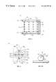
- FIG. 2is a top view of a ring illumination apparatus used to illuminate reflective elements in the inspection system and method according to one embodiment of the present invention
- FIG. 3is a side cross-sectional view of the ring illumination apparatus shown in FIG. 2 taken along line III—III;
- FIG. 4is a side cross-sectional view of the ring illumination apparatus according to another embodiment of the present invention.
- FIG. 5is a schematic view of a reflected image detected by the inspection system according to one embodiment the present invention.
- FIG. 6is a schematic view of a single reflected image element to be processed according to one embodiment of the present invention.
- FIG. 6Ais a side schematic view of a solder ball with light beams reflecting from the point of maximum reflection
- FIG. 7is a flow chart of a method for processing a reflected image according to the present invention.
- FIG. 8is a flow chart of a method for locating one or more points on a reflected image element in a processed reflected image according to the present invention.
- FIG. 9is a flow chart of a method for determining a number of reflected image elements in a reflected image according to the present invention.
- FIG. 10is a schematic view of an inspection system for inspecting one or more surfaces or objects according to an additional embodiment of the present invention.
- FIG. 11is a side schematic view of a solder ball and a solder via illuminated with light beams from a low angle ring light source showing light beams reflecting from the points of maximum reflection;
- FIG. 12is a side schematic view of a solder ball and a solder via illuminated with light beams from an on-axis light source, colinear with the illumination detection device showing light beams reflecting from the points of maximum reflection;
- FIG. 13is an image of a ball and bumped grid array (BGA) illuminated with a low angle ring light source showing both desired and unwanted features;
- BGAball and bumped grid array
- FIG. 14is an image of the same ball and bumped grid array (BGA) shown in FIG. 13, which is illuminated with an on-axis light source, colinear with the illumination detection device, which also shows both desired and unwanted features;
- BGAball and bumped grid array
- FIG. 15is the resulting image calculated by the image processor of the present invention, wherein the image of FIG. 14 is subtracted from the image of FIG. 13, thus eliminating the unwanted features and showing the desired features;
- FIG. 16Ais a graphical depiction of illumination brightness with respect to position along the solder ball and solder via of FIG. 11, when the BGA is illuminated with a low angle ring light source;
- FIG. 16Bis a graphical depiction of illumination brightness with respect to position along the solder ball and solder via of FIG. 12, when the BGA is illuminated with an on-axis light source, colinear with the illumination detection device;
- FIG. 16Cis a graphical depiction of illumination brightness with respect to position along the solder ball and solder via of the resulting image calculated by subtracting the image of FIG. 16B from the image of FIG. 16A;
- FIG. 17is a flow chart of a method of inspecting a BGA to highlight features of interest for image analysis while masking unwanted features;
- FIG. 18is a schematic block diagram of an automated system for inspecting at least one selected reflective feature on an object including a plurality of reflective features using arithmetic operations according to the teachings of the present invention.
- FIG. 19is a flow chart of an inspection method, which applies arithmetic operations to two or more captured reflected images to produce a resulting image with at least one enhanced selected feature of interest.
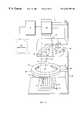
- An inspection system 10is used to inspect one or more reflective elements, such as protruding reflective surfaces or objects 12 , disposed on an article 14 .
- the protruding reflective objects 12are disposed on a generally planar surface 18 that has both reflective and non-reflective areas.
- the article 14typically includes an array of protruding reflective objects 12 made of metal or other light reflective materials.
- the inspection system 10is used to inspect an array of solder balls disposed on metal pads on a chip or other substrate of an electronic component, such as BGA or micro BGA semi-conductor packages, chip scale packaging (CSP), or flex circuits.
- the positioning, size and shape of solder ballsare inspected to facilitate proper electrical connection between the chip and other electronic components, such as printed circuit boards.
- the present inventioncontemplates inspecting any type or shape of reflective elements including, but not limited to, protrusions, deviations, and other contoured surfaces or objects on an article, arranged in any pattern on any type of article.
- the present inspection system 10includes a field of view 16 that covers the protruding reflective objects 12 disposed on the article 14 , and a ring illumination apparatus 20 defining an aperture 22 through which the field of view 16 extends.
- the ring illumination apparatus 20includes a substantially ring-shaped light source 24 that generates light beams 26 and directs the light beams 26 into the field of view 16 on the article 14 such that the protruding reflective objects 12 are illuminated.
- the light beams 26preferably provide a substantially even intensity of light across the field of view 16 on the article 14 and a substantially even illumination of all of the protruding reflective objects 12 in the field of view 16 , as will be described in greater detail below.
- ring illumination apparatus 20may also be in the shape of an oval or other similar shape.
- the inspection system 10further includes an illumination detection device 30 , such as a CCD camera, disposed above the ring illumination apparatus 20 , for example, at about 14 inches above the ring illumination apparatus 20 .
- the illumination detection devicedetects light beams 32 reflected from each protruding reflective object 12 and creates a reflected image.
- an illumination detection device 30is a CCD camera having a resolution of about 640 ⁇ 480 pixels; although the present invention contemplates other types of cameras and devices capable of detecting an illuminated image.
- the substantially ring-shaped light source 24directs light beams 26 at angles of incidence with respect to the article 14 that cause non-detected light beams 34 to reflect from the flat or planar surfaces 18 on the article 14 outside of the field of view 16 or range of the illumination detection device 30 .
- the preferred angles of incidence of the light beams 26are in a range of less than or equal to about 10° and are provided by different embodiments of the substantially ring-shaped light source 24 , as will be described in greater detail below. Accordingly, the detected light beams 32 reflecting from the reflective objects 12 create the reflected image and the non-detected light beams 34 reflecting from flat surfaces 18 are not included in the reflected image.
- the ring illumination apparatus 20can be mounted to a mounting support 28 , for example, with a mounting bracket 29 .
- the mounting support 28 and mounting bracket 29support the ring illumination apparatus 20 in the desired position, allowing the article 14 to be disposed or positioned with the reflective objects 12 in the field of view 16 .
- An article support surface 27 disposed beneath the ring illumination apparatus 20supports the article to be inspected 14 so that the reflective surfaces 12 are in the field of view 16 .
- the article support surface 27is moved to index articles 14 successively into the field of view 16 for inspection during a manufacturing process, as is well known in the art.
- the ring illumination apparatus 20 and illumination detection device 30are indexed or moved over each article 14 being inspected.
- the light source 24preferably uses a strobed power supply that eliminates the effects of motion.
- the inspection system 10further includes an image processor 38 that processes the reflected image and determines inspection information including, but not limited to, the absence/presence, location, pitch, size, and shape of each protruding reflective surface 12 , as will be described in greater detail below.
- the inspection system 10optionally includes a monitor 36 that allows the reflected image to be viewed by an operator.
- the monitor 36facilitates the visual inspection and alignment of the reflective objects 12 by the operator.
- the present inventionalso contemplates other output or peripheral devices including, but not limited to, a printer or storage device.
- the image processor 38can transmit the inspection information to the monitor 36 (if provided) for viewing by the operator or to other peripherals or devices, such as by digital I/O, RS-232 serial communication or Ethernet networking.
- the preferred embodiment of the ring illumination apparatus 20includes a mounting member 40 that defines the aperture 22 and is disposed above the article to be inspected 14 .
- the mounting member 40preferably includes one or more fastener receiving regions 42 , for bolting or otherwise fastening to mounting bracket 29 .
- the mounting member 40can also include a power cord receiving region 44 that receives a power cord connected to a power source (not shown), for powering the light source 24 .
- a power sourcenot shown
- the exemplary embodimentuses a strobed power supply that eliminates the effects of motion on the illumination of articles 14 , the present invention contemplates any type of power source.
- the preferred embodiment of the substantially ring-shaped light source 24includes a plurality of light emitting elements 50 , such as light emitting diodes (LEDs), mounted to the mounting member 40 in a substantially ring shape.
- each light emitting element 50includes an LED that emits light beams having a far red spectral wavelength (e.g. about 660 nanometers) and a beam spread ⁇ of approximately 26° to 28°, such as a TLRA 155BP LED made by Toshiba. CCD cameras respond well to far red LED's which allow the effect of ambient light to be filtered out and substantially eliminated during the inspection process.
- about sixty (60) of such LEDs 50are mounted in a ring around the mounting member 40 .
- the present inventioncontemplates any type and number of light emitting elements that provide the desired even illumination across the field of view.
- the light beams 26are directed at the article 14 in the desired range of angles of incidence by mounting the light emitting elements 50 so that a central axis or center line 54 of each light emitting element 50 is disposed at an angle ⁇ with respect to a plane 52 parallel to the generally planar surface 18 of the article 14 .
- a preferred angle ⁇ of about 4°provides light beams 26 with a low angle of incidence (e.g.
- This embodimentpreferably includes a light reflecting surface 64 , such as white paint or a reflective coating, proximate to each light emitting element 50 and may also include a light diffusing surface 66 generally in front of the light emitting elements 50 , for scattering light and directing light more evenly across the article 14 .
- a light reflecting surface 64such as white paint or a reflective coating
- the angle of reflectionis equal to the angle of incidence, measured from the axis perpendicular to the tangent of the reflective surface. If the angle ⁇ of the light emitting element 50 is too large, the light emitting elements 50 will provide light beams 26 with a high angle of incidence and therefore a high angle of reflection, causing the light beams 26 to reflect off the planar surfaces 18 towards the illumination detection device 30 .
- Lowering the mounting angle ⁇ of the light emitting elements 50therefore lowers the angle of incidence of light beams 26 such that light beams 26 reflect from planar surfaces 18 , such as reflective metalized pads and non-reflective flat surfaces, at a lower angle of reflection outside field of view 16 as non-detected light beams 34 that are not detected by detection device 30 .
- the light beams 26 that hit the protruding reflective objects 12will reflect through the aperture 22 to the illumination detection device 30 as detected light beams 32 .
- the protruding reflective objects 12are thereby illuminated for inspection while the planar surfaces 18 that are not being inspected are not illuminated.
- the angle ⁇ of the light emitting elements 50is also preferably greater than zero to allow sufficient spacing S between the ring illumination apparatus 20 and the article 14 being inspected while ensuring an even illumination across the entire field of view 16 on the article 14 .
- the spacing S of the ring illumination apparatus 20 from the surface 18allows articles 14 to be passed beneath the ring illumination apparatus 20 into and out of the field of view 16 , e.g., when inspecting during a manufacturing process.
- the preferred spacing Sis as small as possible without interfering with the article 14 passing beneath the ring illumination apparatus 20 during the inspection process, and typically in the range of about 1 ⁇ 4 to 1 ⁇ 2 in.
- the light emitting elements 50are also preferably positioned as close as physically possible to the bottom region 56 of the ring illumination apparatus 20 .
- the central light beam area 25 of light beam 26 directed along the center line 54 of each light emitting element 50typically has the highest power or intensity.
- An angle ⁇ of approximately zero (0) degreeswill result in the central light beam area 25 being directed substantially parallel to the article 14 .
- the edges 17 of the field of view 16 on the article 14will only receive lower power or intensity light beams, and protruding reflective objects 12 located proximate to the edges 17 of the field of view 16 may not be sufficiently illuminated.
- a substantially even intensity of light beamsis provided across the entire field of view 16 to provide a substantially even illumination of every protruding reflective object 12 located in the field of view 16 .
- the angle ⁇ of light emitting elements 50is therefore defined so that an imaginary line extending from the center line 54 generally intersects or overlaps the opposite edges or sides 17 of the field of view 16 , but without directing light beams 26 at an angle of incidence high enough to cause detection of light beams reflected from the planar surfaces 18 .
- the substantially ring-shaped light source 24preferably forms a diameter d, e.g., measured from the front portion of the light emitting elements 50 , of approximately 2.5 to 3 times a dimension or width of the field of view 16 on the article 14 .
- This preferred diameter dallows the center light beam area 25 to be directed to the edges 17 with a low angle of incidence while maintaining sufficient spacing S between the ring illumination apparatus 20 and the article 14 .
- a diameter of approximately 5.5 inchesis used to evenly illuminate a field of view 16 on an article 14 of approximately 2 in. by 2 in.
- the diameter d of the ring-shaped light source 24 as well as the angle ⁇ of the light emitting elements 50allow the light beams 26 to provide even illumination across the field of view 16 on the article 14 , while preventing illumination of unwanted planar surfaces 18 and allowing articles 14 to be passed beneath the ring illumination apparatus 20 .
- the preferred embodiment of the ring illumination apparatus 20further includes an upper mounting portion 60 forming the aperture 22 and a side mounting portion 62 extending from the upper mounting portion 60 .
- the plurality of light emitting elements 50are mounted to the side mounting portion 62 which is shaped as a ring and is welded or otherwise secured to the upper mounting portion 60 . Either the light emitting elements 50 or the side mounting portion 62 can be angled to provide the angle ⁇ .
- the light diffusing surface 66can be formed as a light diffusing member or ring mounted to the upper mounting portion 60 .
- the present inventioncontemplates other types of surfaces that diffuse or scatter the light from the light source, such as a light diffusing surface directly disposed on each individual light emitting element 50 .
- the light reflecting surface 64can be provided on the side mounting portion 62 and upper mounting portion 60 .
- the diameter of the aperture 22is approximately 70 to 80 percent the diameter d of the substantially ring-shaped light source 24 such that a portion 65 of the upper mounting portion 60 extends beyond the light emitting elements 50 and has a light reflecting surface 64 .
- the light beams 26are directed at the article 14 in the desired range of angles of incidence with a high transmissivity, high diffusion diffuser 66 a that disperses and angularly scatters light beams as they are emitted from the light emitting elements 50 a .
- the angularly scattered light beams 26 aprovide the substantially even intensity of light across the field of view 16 on the article 14 while preventing illumination of the flat reflective surfaces and allowing the spacing S from the ring illumination apparatus 20 a .
- the angle ⁇ of the of the light emitting elements 50can be eliminated and is preferably in a range of 0° to 8°.
- a light reflecting surface 64is not provided on the portion 65 a of the upper mounting portion 60 a that extends beyond the diffuser 66 .
- This portion of the upper mounting portion 65 acan have a black or other non-reflective surface or can be eliminated entirely.
- the high transmissivity, high diffusion diffuser 66 ahas a diffuse transmission of about 85% or more and preferably in the range of about 88% to 90%.
- One type of high transmissivity, high diffusion diffuser 66 ais an acrylic Diffusing Film Alternative (DFA) manufactured by 3MTM.
- DFADiffusing Film Alternative
- the present inventionalso contemplates other suitable high transmissivity, high diffusion films that provide the desired diffuse transmission and the desired angular scattering of the light beams.
- a larger ring light apparatuscan be used for larger fields of view.
- a smaller ring lightcan be used with conical mirrors that fold the optical path to preserve the internal light path and direct the light beams at the article in the desired angle of incidence range.
- the method of using the inspection system 10 to inspect one or more reflective elements, such as reflective objects 12 , disposed on the article 14includes positioning the article 14 in the field of view 16 .
- Either a series of articles 14are sequentially passed or indexed through the field of view 16 beneath the ring illumination apparatus 20 or the ring illumination apparatus 20 is indexed over each article 14 .
- a ring of light beams 26is directed in a desired range of angles of incidence from the ring illumination apparatus 20 toward the reflective element(s) 12 in the field of view 16 containing, to provide a substantially even intensity of light beams across the field of view 16 without illuminating planar surfaces 18 on the article 14 .
- the system and method of the present inventiondetects light beams reflected from the illuminated reflective elements, such as protruding reflective objects 12 , to form a reflected image 70 , FIG. 5, of the illuminated reflective elements.
- the reflected imageincludes reflected image elements 72 representing the illuminated reflective elements, such as reflective objects 12 .
- the reflected image 70is acquired by converting the analog output signal of the illumination detection device (camera) 30 into a plurality of digital signals, each representing a small picture element or pixel of the image.
- the digital signals forming the reflected image 70can then be converted to analog signals for display on the monitor 36 and/or processed by the image processor 38 (see FIG. 1 ).
- the reflected image 70is processed to determine inspection information including, but not limited to, absence/presence, location, size, and shape of the reflective elements.
- the inspection system 10is used to inspect an array of solder balls disposed on solder pads on an electronic component, such as a semiconductor chip.
- each solder ballappears as a reflected image element 72 , FIG. 6, having a “doughnut” or ring shape.
- the inspection information pertaining to the array of solder ballsincludes, but is not limited to, absence/presence of each solder ball in the array, location of each solder ball, the pitch between solder balls, malformed solder balls, the diameter of each solder ball, and the circularity of each solder ball.
- the present inventionalso features a method 100 , FIG. 7, of processing a reflected image 70 including a pattern of reflected image elements 72 .
- the method of processing the reflected imageincludes locating the pattern of reflected image elements 72 in the reflected image 70 , step 110 ; fitting an outline to each reflected image element 72 in the pattern of reflected image elements, step 120 ; and determining inspection information pertaining to the reflective elements represented by the reflected image 70 , step 130 .
- One way of locating the pattern of reflected image elements 72 , step 110is by identifying a group of reflected image elements 72 , for example, by creating a window 75 (FIG. 5) around an outside row or group of reflected image elements 72 . A point on each reflected image element 72 in the group, such as an outside edge 76 , is then located. One or more lines 74 are fit to the outside edges 76 or other point on the reflected image elements 72 (see FIG. 5) to locate the pattern and determine the “expected” location of each reflected image element 72 in the pattern.
- the exemplary embodimentshows a rectangular grid of image elements 72
- the present inventionalso contemplates locating a circular or other pattern of reflected image elements. In a circular pattern, the outside edges of the image elements formed in a circle are located and a circle fit algorithm is used to fit a circle to the outside edges and to locate the pattern.
- Another way of locating the reflected imageis by locating reference marks or fiducials 73 disposed in predetermined locations with respect to the reflected image elements 72 in the reflected image 70 .
- a further way of locating the reflected imageis by correlating a template or model of a known pattern with the reflected image.
- the outlineis fit to each reflected image element, step 120 , for example, by creating a window 78 (FIG. 6) around each reflected image element 72 at each expected location and locating multiple points 76 a - 76 d on the edge 76 of the reflected image element 72 or locating multiple midpoints 71 a - 71 d within the reflected image element 72 .
- a reflected image element 72 having a circular or ring shapeat least three of the edge points 76 a - 76 d or midpoints 71 a - 71 d are needed to fit the respective circular outline 77 a , 77 b .
- edge points 76 a - 76 d or midpoints 71 a - 71 dare needed to determine the circularity of the respective outline 77 a , 77 b .
- the edge points 76 a - 76 d or midpoints 71 a - 71 d and respective outlines 77 a , 77 b fit to the image element(s) 72correspond to a known percentage of the true the diameter, circularity, or other dimension of the solder ball or other reflective element being measured, as described in greater detail below.
- eight (8) or more pointsare located, and the locations of the points are fed to a circle fit algorithm which accurately determines the size and circularity of the reflective elements.
- the method 200 , FIG. 8, of locating the points 76 a - 76 d on the outside edge 76 or the midpoints 71 a - 71 d of each reflected image element 72includes dividing the reflected image 70 into a plurality of pixels having a gray scale value corresponding to an intensity level of reflected light in the reflected image 70 , step 210 .
- each pixelis represented by eight (8) bits with a gray scale value of zero (0) being the darkest pixel and a gray scale value of 255 being the brightest pixel.
- Vectors 79 a - 79 d(FIG. 6) are positioned to intersect the expected location of the image element 72 , step 220 .
- a series of pixels along each vector 79 a - 79 dis examined to find edge points 76 a - 76 d or midpoints 71 a - 71 d , step 230 , along the vectors 79 a - 79 b .
- the vectorscan be positioned in various configurations, such as a cross-hatched configuration, provided that the vectors intersect the image element 72 .
- the edge points 76 a - 76 d or midpoints 71 a - 71 dare then used to locate the image by fitting the line 74 or to determine a diameter, circularity or other dimension of the solder ball by fitting the outline 77 a , 77 b , as describe above.
- an intensity gradient at each pixelis determined by differentiating between the gray scale values of pixels on either side of each pixel.
- the point of maximum gradienti.e. the steepest or greatest change from darkest to brightest pixels
- the preferred methodincludes taking a group of points having the highest intensity gradients for each reflected image element 72 and fitting an ellipse to the highest intensity gradients.
- the peak of the ellipsecorresponds to the point of highest intensity gradient with sub-pixel accuracy, thereby allowing a more accurate calculation of the dimensions and shape of the solder ball or other reflective surface represented by each reflected image element 72 .
- the edge points 76 a - 76 d and circular outline 77 a fit to the edge points 76 a - 76 dcorrespond to a known percentage of the true dimensions of the solder ball being measured, e.g. about 70%.
- a gray scale value at each pixelis determined and the midpoint 71 in the ring shaped image element 72 corresponds to the pixel having the highest gray scale value.
- the preferred methodincludes taking a group of pixels having the highest gray scale value, e.g. the brightest pixel and one or more adjacent pixels, and fitting an ellipse to these pixels. The peak of the ellipse corresponds to the midpoint 71 having the highest intensity with sub-pixel accuracy.
- the brightest midpoints 71 a - 71 d and the circular outline 77 b fit to midpoints 71 a - 71 dcorrespond to a known dimension of the solder ball being measured.
- Each solder ball 80FIG. 6A, has point 82 of maximum reflection located on the spherical surface of the solder ball 82 at about 45° from the top that reflects light beams 84 of the highest intensity.
- the location of the point 82 of maximum reflectionis equal to sin(45°) (or 0.7071) times the diameter of the solder ball 80 .
- the brightest midpoints 71 a - 71 d and the circular outline 77 btherefore correspond to the point(s) 82 of maximum reflection and the known percentage of the true diameter of the solder ball 80 .
- Using the brightest midpoint 71 a - 71 d of the image element 72provides a truer measurement than using the intensity gradient method to locate the edge points 76 a - 76 d of the image element 72 if the edges 76 of the image elements 72 are not focused.
- the present image processing methodfurther includes a method 300 , FIG. 9, of determining the number of reflected image elements 72 . Determining the number of reflected image elements 72 in the entire reflected image 70 , not just at the expected locations, allows the absence/presence of solder balls or other reflective surfaces to be easily determined.
- the number of reflected image elements 72is determined by dividing the reflected image 70 into a plurality of pixels having a gray scale value corresponding to the intensity of light in the reflected image 70 , step 310 . Groups of pixels having a gray scale value above a threshold value are then located, step 320 , and the number of groups of pixels (corresponding to the number of reflected image elements 72 ) are counted, step 330 . Determining the number of reflected image elements 72 allows a determination of missing, misplaced or extra reflective elements, such as solder balls or other reflective objects.
- the image processing method of the present inventionalso includes a calibration process that can be performed to allow the inspection information measurements to be expressed in conventional units and to correct for magnification, perspective errors, and other effects.
- the calibration procedureinvolves measuring a target of known dimensions, for example, an array of dots having known sizes and known locations on the target. The relationship between the coordinates of the target image as determined by the image processor and the known location of the dots on the target are calculated to determine the correlation between pixels and conventional units.
- the present methodalso contemplates height correction of the part being inspected relative to the calibration target to account for errors caused by optical magnification.
- the present method for processing the reflected image 70 used together with the ring illumination apparatus 20 described aboveprovides a more accurate determination of the diameter and circularity of solder balls on an electronic component or other article.
- Directing the light beams in the desired range of angles of incidencee.g. by angling the light source 24 at an angle ⁇ , by using a high diffusion diffuser, or by using conical mirrors, illuminates a portion of the top surface of each solder ball so that the point of maximum gradient or highest gray scale value corresponds to a known percentage of the true diameter of the solder ball.
- Directing the light beams in the desired range of angles of incidencealso prevents illumination of solder pads or other generally planar surface areas from interfering with the determination of the maximum gradient.
- the ring illumination apparatus of the present inventionWhen the ring illumination apparatus of the present invention is used together with the present method of processing the reflected image, the measurements made during the inspection have a high degree of accuracy and repeatability.
- the present inventioncontemplates using the ring illumination apparatus with other methods for processing the reflected image as well as using this method of processing the reflected image with another type of illumination apparatus.
- FIG. 10One such alternative embodiment is shown in FIG. 10 .
- a second light source 90is added to the ring illumination apparatus and inspection system described in detail above.
- Communication elements found in the embodiments of FIGS. 1 and 10are designated using common reference numbers.
- the apparatus of FIG. 10uses the principle of image subtraction to eliminate or mask the unwanted features of the image. For example when a ball and bumped grid array (BGA) is inspected both the solder balls, which are desired to be inspected and solder vias intermediate the balls may appear similarly when the BGA is illuminated by a single illumination apparatus.
- BGAball and bumped grid array
- the principle of image subtractionrequires the illumination of the article to be inspected by at least two different light sources and the capturing of at least two different images of the article as it is illuminated using the different light sources.
- the different light sourcesare selected so that they illuminate the unwanted features similarly, while at the same time illuminate the desired features differently.
- the unwanted featureswhich appear substantially the same in both images, subtract out to 0.
- the desired featuresappear different in the two captured images, they do not subtract out. In fact, they will either remain the same or be enhanced by the image subtraction process.
- the image resulting from the image subtraction processwill contain only the desired features, which can then be analyzed normally.
- a second illumination apparatusis mounted to mounting support 28 .
- the second illumination apparatusis an on-axis illumination apparatus 90 , which provides on-axis illumination of the article to be inspected 14 , substantially co-linearly with the illumination detection device 30 .
- the on-axis illumination apparatus 90includes light source 92 and beam splitter 94 .
- the beam splitter 94is positioned within the field of view 16 and, in the preferred embodiment is located above the ring illumination apparatus 20 .
- the beam splitter 94re-directs the light beams 96 generated by light source 92 towards the article to be inspected.
- the re-directed light beams 96 aare substantially co-linear with the axis of the illumination detection device 30 in order to provide the desired effects of the use of multiple illumination apparatuses, which will be discussed in more detail below.
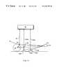
- FIG. 11shows the orientation of a solder ball 80 and a solder via 80 a on a BGA being inspected by the inspection apparatus 10 .
- each solder ball 80has point 82 of maximum reflection of light beam 84 , which is located on the spherical surface of the solder ball 82 at about 45° from the top of the ball. This location of maximum reflection 82 directs reflected light beams 84 a of the highest intensity.
- each solder via 80 ahas points 82 a of maximum reflection located substantially adjacent to each peak of the solder via 80 a , where the surface of the solder via is oriented substantially 45° with respect the axis of the illumination detection device 30 .
- the solder ball 80 and solder via 80 aare three-dimensional objects, the former being a sphere and the later being a disc having a circular shaped ring of maximum thickness.
- the resulting image captured by the illumination detection device 30will appear as a grid of illuminated rings (FIG. 13 ). These illuminated rings correspond to the 45 degree surfaces of the solder balls and the solder vias, which reflect light from the ring light source 20 into the illumination detection device.
- the solder balls 80appear as large bright rings 86 and the solder vias appear as smaller bright rings 88 .
- a two-dimensional graph of image brightness with respect to position on each solder ball and solder via illuminated using the ring illumination source according to FIG. 11is shown in FIG. 16 A.
- the bright rings that represent the solder viasare similar in brightness to those that represent the solder balls. Accordingly, they may interfere with the image analysis. Thus, their elimination from the image to be analyzed is desirable.
- the article to be inspected 14is next illuminated by the second, different light source and a second image of the article is captured by the illumination detection device 30 .
- the articlemay be illuminated by the on-axis illumination source 90 of FIG. 10 .
- An on-axis illumination sourceis selected since it will illuminate the article to be inspected 14 in such a manner that the solder vias 80 a will appear substantially the same to the illumination detection device 30 as they appear when illuminated using the ring illumination source of FIG. 11 .
- Light rays 96are emitted from light source 92 and are directed to beam splitter 94 , which reflects the light rays toward the solder balls 80 and solder vias 80 a as incident light rays 96 a , which are substantially colinear with the axis of the illumination detection device 30 . As can be seen, only those incident light rays 96 a that reflect off of horizontal surfaces will be reflected back up to the illumination detection device 30 , where they will be captured as a second image of the article being inspected 14 .
- the second image of the articleis shown in FIG. 14 and includes a plurality of bright dots 97 and bright rings 98 .
- the bright dotsare the reflections received from the top of the solder balls 80 .
- the solder vias 80 aappear as the bright rings 98 because the incident light rays 96 a reflecting off the flat top of the crater-like via is captured by the illumination detection device 30 .
- FIG. 16 BA two-dimensional graph of image brightness with respect to position on each solder ball and solder via illuminated using the on-axis illumination source according to FIG. 12 is shown in FIG. 16 B.
- the graph of image brightness of the solder vias of FIGS. 16A and 16Bare compared, it is evident that the images of the solder vias are substantially the same, although not identical.
- the second captured imagewhich is the image captured when the article is illuminated using the on-axis illumination source is then subtracted from the first captured image, which is the image captured when the article is illuminated using the ring illumination source.
- the result of image subtractionis that the images of the solder vias substantially cancel each other out, while the image of the solder balls do not.
- the resulting imagewould only include the desired features, which, in this case are the solder balls.
- the image resulting from the above-specified image subtraction operationis shown in FIG. 15 .
- the unwanted featuresnamely the solder vias, are eliminated within the search box.
- the solder ballswhich are the desired features of the article being inspected appear as bright rings 99 .
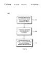
- a method of image subtraction 400is shown in FIG. 17 .
- the methodbegins by illuminating an article to be inspected with a first illumination source, step 410 . Once the article is illuminated, a first image of the article is captured using an illumination detection device, such as a CCD camera, step 420 . The first image is then stored in an image buffer, step 430 .
- the article to be inspectedis then illuminated by a second illumination source, which is selected such that the desired features of the article will be illuminated differently by the second illumination source than they were with the first illumination source and the unwanted features will be illuminated substantially the same as they were illuminated by the first illumination source, step 440 .
- a second image of the articleis captured by the image capture device, step 450 , an is stored in the image buffer, step 460 .
- the imagesare then processed by an image processor, which subtracts one image from the other to generate a resulting image, step 470 .
- the first imagemay be subtracted from the second image.
- the second imagemay be subtracted from the first.
- the subtraction processwill substantially eliminate them from the resulting image.
- the resulting imagewill be substantially devoid of the unwanted features.
- the resulting imagewill then be stored in the image buffer, step 480 .
- the resulting imagemay then be analyzed using additional image analysis techniques.
- additional image arithmetic operationscan be utilized to selectively enhance selected reflective features on an object being inspected that includes a plurality of reflective features.
- a system 500 capable of applying any one of a number of arithmetic operationsis shown in FIG. 18 .
- a key requirement of the disclosed automated inspection systemis that the system must include a first illumination apparatus 502 and at least one additional illumination apparatus 504 , which is different from the first illumination apparatus. This plurality of illumination apparatuses are used to sequentially illuminate an object 506 being inspected, which includes a plurality of reflective features 508 .
- the underlying principleis that illuminating an object that includes a plurality of reflective features using differing illumination apparatuses will result in different reflected images of the object.
- the plurality of illumination apparatuses 502 & 504 a-nmust differ in some way in order to produce differences in the reflected images associated therewith. Examples of differences in illumination apparatuses include differences in geometric arrangement, such as high or low angle ring lights, or differently arranged point sources.
- the different illumination apparatusesmay differ in degree of diffusion or in other characteristic such as color or polarization.
- a separate reflected image of the object 506 and the plurality of reflective features 508 included thereonis captured by an illumination capture device 30 , such as the CCD camera described above.
- Each captured imagewill be stored in an image buffer 510 included in image processor 38 .
- stored in the image buffer 510will be a first reflected image of the object being inspected, which corresponds to the object when it was illuminated with the first illumination apparatus 502 .
- the image processor 38performs one or more arithmetic operation on the images to produce a resulting image.
- the specific reflected images processed and arithmetic operation(s) selectedare chosen so as to produce resulting image(s) wherein one or more selected reflective features are enhanced.
- the arithmetic operationsmay be selected from the group consisting of addition, multiplication, division or other mathematical combinations. Additionally, the arithmetic operation selected may be a logical operation, such as AND or XOR. Furthermore, statistical arithmetic operations, such as “maximum value” or a “range of values” may be applied to the reflected images stored in the image buffer.
- the arithmetic operationsthus produce resulting images that enhance one or more selected feature.
- the resulting image(s)may then be provided to additional image analysis equipment 512 , which may include additional computer hardware and software programmed to inspect the selected features enhanced in the resulting image. For example, defects, such as scratches, voids and pits in plastic overmolding on electronic packages may be readily identified.
- this additional embodimentmay also include an optional monitor 36 , which may be viewed in real time by a system operator while objects are being inspected to assist in, augment or manage the inspection process.
- FIG. 19One embodiment of an inspection method 600 , which applies arithmetic operations to two or more captured reflected images to produce a resulting image with at least one enhanced selected feature of interest, is shown in FIG. 19 .
- the methodbegins with the illumination of an object including a plurality of features by a first illumination apparatus, step 605 . Once the object being inspected is illuminated, a first reflected image of the plurality of features is captured by an illumination detection device, such as a CCD camera, step 610 . The first reflected image is stored in an image buffer, step 615 .
- each additional illumination apparatusis selected so that it is different in either geometrical arrangement, such as high or low angle ring lights, partial ring lights and area array light sources or is different in degree of diffusion or lighting characteristic, such as color or polarization.
- the object of using different illumination apparatusesis that each additional illumination apparatus will reflect differently off of the plurality of features included on the object being inspected, which will result in a different reflected image. Since each reflected image of the object being inspected is captured using a single illumination detection device, which is stationary with respect to the object being inspected, all of the features included on the object will be in registration with each other (i.e., they will appear in the same position on the object in each image). However, since they will be illuminated by differing illumination apparatuses, they may appear differently in the plurality of captured images.
- Each additional reflected image of the object being inspectedwill then be captured by the illumination detection device, step 625 , and stored in an image buffer, step 630 .
- an image processorwhich will combine at least two reflected images using at least one arithmetic operation to create a resulting image in which at least one selected feature is enhanced, step 635 .
- the combination of the imagesmay be performed using simple arithmetic or complex mathematical operations on gray-scale values, including addition, multiplication, division or other combinations of mathematical operations.
- logical operationssuch as AND or XOR may be applied to the images.
- statistical operationssuch as maximum value or range of values may be applied.
- the resulting image, in which selected features are enhanced,can then be inspected using additional image processing equipment, including computer hardware and software to adequately inspect the selected features of interest according to specifications applicable to the specific features, step 640 .
- the steps of illuminating the object, capturing images or the object, storing the captured images and combining the captured imagesmay be repeated any number of times until all of the features of interest are adequately inspected.
- the disclosed methodcan be performed in combination with other inspection methods, such as the image subtraction method disclosed in commonly owned, co-pending patent application identified by Ser. No. 09/134,654, which is being filed near contemporaneously herewith.
- the present inventionprovides an inspection system and method that enhances the detectability of selected reflective features on an object being inspected, such as solder balls, protrusions, intrusions, deviations, concavities, data matrices, one and two-dimensional identification codes, the shapes of certain features, such as solder joints, as well as other reflective or non-reflective features on an article, including missing features.
- selected reflective features on an object being inspectedsuch as solder balls, protrusions, intrusions, deviations, concavities, data matrices, one and two-dimensional identification codes, the shapes of certain features, such as solder joints, as well as other reflective or non-reflective features on an article, including missing features.
Landscapes
- Engineering & Computer Science (AREA)
- General Physics & Mathematics (AREA)
- Physics & Mathematics (AREA)
- General Health & Medical Sciences (AREA)
- Health & Medical Sciences (AREA)
- Analytical Chemistry (AREA)
- Life Sciences & Earth Sciences (AREA)
- Theoretical Computer Science (AREA)
- Pathology (AREA)
- Immunology (AREA)
- Biochemistry (AREA)
- Chemical & Material Sciences (AREA)
- Microelectronics & Electronic Packaging (AREA)
- Multimedia (AREA)
- Manufacturing & Machinery (AREA)
- Vascular Medicine (AREA)
- Operations Research (AREA)
- Computer Vision & Pattern Recognition (AREA)
- Quality & Reliability (AREA)
- Investigating Materials By The Use Of Optical Means Adapted For Particular Applications (AREA)
- Length Measuring Devices By Optical Means (AREA)
Abstract
Description
Claims (17)
Priority Applications (5)
| Application Number | Priority Date | Filing Date | Title |
|---|---|---|---|
| US09/134,397US6201892B1 (en) | 1997-02-26 | 1998-08-14 | System and method for arithmetic operations for electronic package inspection |
| EP99940972AEP1127329A4 (en) | 1998-08-14 | 1999-08-09 | System and method for arithmetic operations for electronic package inspection |
| PCT/US1999/017985WO2000010114A1 (en) | 1998-08-14 | 1999-08-09 | System and method for arithmetic operations for electronic package inspection |
| CA002340420ACA2340420A1 (en) | 1998-08-14 | 1999-08-09 | System and method for arithmetic operations for electronic package inspection |
| AU54715/99AAU5471599A (en) | 1998-08-14 | 1999-08-09 | System and method for arithmetic operations for electronic package inspection |
Applications Claiming Priority (3)
| Application Number | Priority Date | Filing Date | Title |
|---|---|---|---|
| US08/807,397US5943125A (en) | 1997-02-26 | 1997-02-26 | Ring illumination apparatus for illuminating reflective elements on a generally planar surface |
| US08/824,173US5926557A (en) | 1997-02-26 | 1997-03-26 | Inspection method |
| US09/134,397US6201892B1 (en) | 1997-02-26 | 1998-08-14 | System and method for arithmetic operations for electronic package inspection |
Related Parent Applications (1)
| Application Number | Title | Priority Date | Filing Date |
|---|---|---|---|
| US08/824,173Continuation-In-PartUS5926557A (en) | 1997-02-26 | 1997-03-26 | Inspection method |
Publications (1)
| Publication Number | Publication Date |
|---|---|
| US6201892B1true US6201892B1 (en) | 2001-03-13 |
Family
ID=22463193
Family Applications (1)
| Application Number | Title | Priority Date | Filing Date |
|---|---|---|---|
| US09/134,397Expired - LifetimeUS6201892B1 (en) | 1997-02-26 | 1998-08-14 | System and method for arithmetic operations for electronic package inspection |
Country Status (5)
| Country | Link |
|---|---|
| US (1) | US6201892B1 (en) |
| EP (1) | EP1127329A4 (en) |
| AU (1) | AU5471599A (en) |
| CA (1) | CA2340420A1 (en) |
| WO (1) | WO2000010114A1 (en) |
Cited By (45)
| Publication number | Priority date | Publication date | Assignee | Title |
|---|---|---|---|---|
| US6356300B1 (en)* | 1998-01-16 | 2002-03-12 | Nec Corporation | Automatic visual inspection apparatus automatic visual inspection method and recording medium having recorded an automatic visual inspection program |
| US20020191834A1 (en)* | 2000-01-07 | 2002-12-19 | David Fishbaine | High speed optical image acquisition system with extended dynamic range |
| US20030103756A1 (en)* | 2001-12-04 | 2003-06-05 | Canty Thomas M. | Modular insertion device for process illumination and viewing |
| US6630998B1 (en)* | 1998-08-13 | 2003-10-07 | Acushnet Company | Apparatus and method for automated game ball inspection |
| US20030206650A1 (en)* | 2002-05-02 | 2003-11-06 | Mitutoyo Corporation | Systems and methods for continuously varying wavelength illumination |
| WO2004023209A1 (en)* | 2002-09-04 | 2004-03-18 | Brooks Automation, Inc. | Device and process for reading out identification information on reticles |
| US20040085549A1 (en)* | 2000-12-29 | 2004-05-06 | Carl Smets | Method and an apparatus for measuring positions of contact elements of an electronic component |
| US6750899B1 (en) | 2000-01-07 | 2004-06-15 | Cyberoptics Corporation | Solder paste inspection system |
| US6758384B2 (en)* | 2001-05-03 | 2004-07-06 | Samsung Electronics Co., Ltd. | Three-dimensional soldering inspection apparatus and method |
| US6762428B2 (en)* | 2000-07-17 | 2004-07-13 | Nagoya Electric Works Co. Ltd. | Cream solder inspection method and apparatus therefor |
| US6765185B2 (en)* | 2001-10-04 | 2004-07-20 | Koninklijke Philips Electronics N.V. | Computer vision recognition of metallic objects against a poorly contrasting background |
| US20040141175A1 (en)* | 2002-07-12 | 2004-07-22 | Leo Baldwin | Method and apparatus for uniform lighting source |
| US6778282B1 (en)* | 1999-04-13 | 2004-08-17 | Icos Vision Systems N.V. | Measuring positions of coplanarity of contract elements of an electronic component with a flat illumination and two cameras |
| US20040175027A1 (en)* | 2003-03-07 | 2004-09-09 | James Mahon | Machine vision inspection system and method |
| US20050073590A1 (en)* | 2002-02-01 | 2005-04-07 | Takahiro Mamiya | Three-dimensional measuring instrument, filter striped plate, and illuminating means |
| US20060040442A1 (en)* | 2004-06-01 | 2006-02-23 | Takayuki Fukae | Bump inspection apparatus and method for IC component, bump forming method for IC component, and mounting method for IC component |
| US20060140485A1 (en)* | 2004-12-28 | 2006-06-29 | Hing Cheung C | Method and apparatus for detecting an image of a reflective object |
| US20070009257A1 (en)* | 2005-07-08 | 2007-01-11 | Leo Baldwin | Optimizing use and performance of optical systems implemented with telecentric on-axis dark field illumination |
| US7200259B1 (en)* | 1999-07-25 | 2007-04-03 | Orbotech Ltd. | Optical inspection system |
| US20070217675A1 (en)* | 2006-03-15 | 2007-09-20 | International Business Machines Corporation | Z-axis optical detection of mechanical feature height |
| US20080199068A1 (en)* | 2007-01-10 | 2008-08-21 | Duquette David W | Inspection System |
| US20100033721A1 (en)* | 2008-08-07 | 2010-02-11 | Gwangji Institute of Science and Technology | System and method for measuring reflectance of object |
| US20100128964A1 (en)* | 2008-11-25 | 2010-05-27 | Ronald Bruce Blair | Sequenced Illumination |
| US20110052082A1 (en)* | 2009-09-02 | 2011-03-03 | De La Rue North America Inc. | Systems and Methods for Detecting Tape on a Document |
| US20110105740A1 (en)* | 2005-11-10 | 2011-05-05 | SANTARIS PHARMA A/S, a Denmark corporation | Soluble tnf receptors and their use in treatment of disease |
| US20110164804A1 (en)* | 2010-01-07 | 2011-07-07 | De La Rue North America Inc. | Detection of Color Shifting Elements Using Sequenced Illumination |
| US20110255768A1 (en)* | 2010-04-14 | 2011-10-20 | Oracle International Corporation | Method and System for Automated Ball-Grid Array Void Quantification |
| US8059280B2 (en) | 2008-01-31 | 2011-11-15 | Cyberoptics Corporation | Method for three-dimensional imaging using multi-phase structured light |
| US8223200B1 (en) | 2009-06-09 | 2012-07-17 | Hormel Foods Corporation | Package vision evaluation system |
| JP2013057561A (en)* | 2011-09-07 | 2013-03-28 | Shibuya Kogyo Co Ltd | Method for setting preset value for lighting of article recognition device, and article recognition device |
| US20140055598A1 (en)* | 2012-08-27 | 2014-02-27 | Yamaha Hatsudoki Kabushiki Kaisha | Semiconductor component mounting apparatus |
| EP1864146B1 (en)* | 2004-11-24 | 2014-03-12 | Stratus Vision GmbH | Inspection device |
| US8682038B2 (en) | 2008-11-25 | 2014-03-25 | De La Rue North America Inc. | Determining document fitness using illumination |
| US20150146970A1 (en)* | 2013-11-25 | 2015-05-28 | International Business Machines Corporation | Spherical lighting device with backlighting coronal ring |
| US9053596B2 (en) | 2012-07-31 | 2015-06-09 | De La Rue North America Inc. | Systems and methods for spectral authentication of a feature of a document |
| US20170089841A1 (en)* | 2015-09-30 | 2017-03-30 | Canon Kabushiki Kaisha | Inspection apparatus and article manufacturing method |
| US20170352150A1 (en)* | 2014-12-27 | 2017-12-07 | Hill's Pet Nutrition, Inc. | Food Processing Method and System |
| US10126252B2 (en) | 2013-04-29 | 2018-11-13 | Cyberoptics Corporation | Enhanced illumination control for three-dimensional imaging |
| US20190227002A1 (en)* | 2018-01-24 | 2019-07-25 | Corning Incorporated | Apparatus and methods for inspecting damage intensity |
| US10499487B2 (en) | 2015-10-05 | 2019-12-03 | Scalia Lighting Technologies LLC | Light-emitting diode (LED) lighting fixture solutions and methods |
| US20200240925A1 (en)* | 2018-10-11 | 2020-07-30 | Nanotronics Imaging, Inc. | Macro inspection systems, apparatus and methods |
| US20200364442A1 (en)* | 2019-05-15 | 2020-11-19 | Getac Technology Corporation | System for detecting surface pattern of object and artificial neural network-based method for detecting surface pattern of object |
| US20220148155A1 (en)* | 2019-04-10 | 2022-05-12 | Doss Visual Solution S.R.L. | Method of acquiring images for an optical inspection machine |
| US11961210B2 (en) | 2019-08-07 | 2024-04-16 | Nanotronics Imaging, Inc. | System, method and apparatus for macroscopic inspection of reflective specimens |
| US11995802B2 (en) | 2019-08-07 | 2024-05-28 | Nanotronics Imaging, Inc. | System, method and apparatus for macroscopic inspection of reflective specimens |
Families Citing this family (6)
| Publication number | Priority date | Publication date | Assignee | Title |
|---|---|---|---|---|
| FR2804784B1 (en) | 2000-02-04 | 2003-04-11 | Novatec | UNIVERSAL PROCESS FOR THE IDENTIFICATION AND AUTHENTICATION OF OBJECTS, PLANTS OR LIVING BEINGS |
| US6552783B1 (en) | 2000-06-28 | 2003-04-22 | Teradyne, Inc. | Optical system |
| WO2002027267A1 (en)* | 2000-09-29 | 2002-04-04 | Bernd Sommer | Optical ball height measurement of ball grid arrays |
| DE10239548A1 (en)* | 2002-08-23 | 2004-03-04 | Leica Microsystems Semiconductor Gmbh | Device and method for inspecting an object |
| US7019826B2 (en) | 2003-03-20 | 2006-03-28 | Agilent Technologies, Inc. | Optical inspection system, apparatus and method for reconstructing three-dimensional images for printed circuit board and electronics manufacturing inspection |
| GB2443457B (en) | 2006-10-31 | 2011-11-02 | Hewlett Packard Development Co | Image processing system and method |
Citations (45)
| Publication number | Priority date | Publication date | Assignee | Title |
|---|---|---|---|---|
| US4028728A (en) | 1976-04-02 | 1977-06-07 | Western Electric Company, Inc. | Method of and video system for identifying different light-reflective surface areas on articles |
| US4677473A (en) | 1985-06-21 | 1987-06-30 | Matsushita Electric Works, Ltd. | Soldering inspection system and method therefor |
| US4688935A (en) | 1983-06-24 | 1987-08-25 | Morton Thiokol, Inc. | Plasma spectroscopic analysis of organometallic compounds |
| US4688939A (en) | 1985-12-27 | 1987-08-25 | At&T Technologies, Inc. | Method and apparatus for inspecting articles |
| US4695157A (en) | 1985-10-11 | 1987-09-22 | Benchmark Industries Incorporated | Solder process inspection diffuser assembly |
| US4697076A (en) | 1984-05-24 | 1987-09-29 | Hajime Industries, Ltd. | Lighting device for inspecting objects for flaws |
| US4782238A (en)* | 1987-10-20 | 1988-11-01 | Eastman Kodak Company | Apparatus for generating edge position signals for use in locating an address element on a mailpiece |
| US4972093A (en) | 1987-10-09 | 1990-11-20 | Pressco Inc. | Inspection lighting system |
| US4988202A (en) | 1989-06-28 | 1991-01-29 | Westinghouse Electric Corp. | Solder joint inspection system and method |
| US5023916A (en) | 1989-08-28 | 1991-06-11 | Hewlett-Packard Company | Method for inspecting the leads of electrical components on surface mount printed circuit boards |
| US5030008A (en) | 1988-10-11 | 1991-07-09 | Kla Instruments, Corporation | Method and apparatus for the automated analysis of three-dimensional objects |
| US5039868A (en) | 1988-11-24 | 1991-08-13 | Omron Corporation | Method of and apparatus for inspecting printed circuit boards and the like |
| US5051872A (en) | 1988-07-19 | 1991-09-24 | Texas Instruments Incorporated | Hemispherical non-glare illuminator |
| US5058178A (en) | 1989-12-21 | 1991-10-15 | At&T Bell Laboratories | Method and apparatus for inspection of specular, three-dimensional features |
| US5064291A (en) | 1990-04-03 | 1991-11-12 | Hughes Aircraft Company | Method and apparatus for inspection of solder joints utilizing shape determination from shading |
| US5072127A (en) | 1987-10-09 | 1991-12-10 | Pressco, Inc. | Engineered video inspecting lighting array |
| US5097516A (en) | 1991-02-28 | 1992-03-17 | At&T Bell Laboratories | Technique for illuminating a surface with a gradient intensity line of light to achieve enhanced two-dimensional imaging |
| US5118193A (en) | 1990-03-19 | 1992-06-02 | Texas Instruments Incorporated | Apparatus and method for inspection |
| US5127727A (en) | 1991-05-30 | 1992-07-07 | Northern Telecom Limited | Illumination devices for inspection systems |
| US5137362A (en) | 1990-03-26 | 1992-08-11 | Motorola, Inc. | Automatic package inspection method |
| US5166985A (en) | 1990-04-18 | 1992-11-24 | Hitachi, Ltd. | Method and apparatus for inspecting surface pattern of object |
| US5245671A (en) | 1988-05-09 | 1993-09-14 | Omron Corporation | Apparatus for inspecting printed circuit boards and the like, and method of operating same |
| US5247344A (en) | 1988-10-03 | 1993-09-21 | Hughes Aircraft Company | Optical inspection system for solder joints and inspection method |
| US5257714A (en) | 1990-11-20 | 1993-11-02 | International Business Machines Corporation | Method and apparatus for electronic component lead inspection |
| US5267217A (en) | 1990-03-20 | 1993-11-30 | Matsushita Electric Industrial Co., Ltd. | Apparatus for and method of detecting shape of solder portion |
| US5302836A (en) | 1992-07-16 | 1994-04-12 | Bernard Siu | High speed image acquisition for microelectronics inspection |
| US5394246A (en) | 1991-12-02 | 1995-02-28 | Kabushiki Kaisha Shinkawa | Bonding wire inspection apparatus and method |
| US5406372A (en) | 1993-04-16 | 1995-04-11 | Modular Vision Systems Inc. | QFP lead quality inspection system and method |
| US5418879A (en) | 1994-04-04 | 1995-05-23 | Chrysler Corporation | Distributed light delivery system |
| US5420689A (en) | 1993-03-01 | 1995-05-30 | Siu; Bernard | High speed illumination system for microelectronics inspection |
| US5424838A (en) | 1993-03-01 | 1995-06-13 | Siu; Bernard | Microelectronics inspection system |
| US5440391A (en) | 1990-03-23 | 1995-08-08 | Icos Vision Systems N.V. | Method and device for determining a position of at least one lead of an electronic component |
| US5461417A (en) | 1993-02-16 | 1995-10-24 | Northeast Robotics, Inc. | Continuous diffuse illumination method and apparatus |
| US5495424A (en) | 1990-04-18 | 1996-02-27 | Matsushita Electric Industrial Co., Ltd. | Method and apparatus for inspecting solder portions |
| US5519496A (en) | 1994-01-07 | 1996-05-21 | Applied Intelligent Systems, Inc. | Illumination system and method for generating an image of an object |
| US5533146A (en) | 1991-09-11 | 1996-07-02 | Toyota Jidosha Kabushiki Kaisha | Weld bead quality determining apparatus |
| US5539485A (en) | 1994-10-31 | 1996-07-23 | White; Timothy P. | Illumination device for providing continuous diffuse light on and off an observing axis |
| US5574801A (en) | 1993-08-12 | 1996-11-12 | Collet-Beillon; Olivier | Method of inspecting an array of solder ball connections of an integrated circuit module |
| US5581632A (en) | 1994-05-02 | 1996-12-03 | Cognex Corporation | Method and apparatus for ball bond inspection system |
| US5598345A (en) | 1990-11-29 | 1997-01-28 | Matsushita Electric Industrial Co., Ltd. | Method and apparatus for inspecting solder portions |
| US5604550A (en) | 1994-10-31 | 1997-02-18 | Northeast Robotics, Inc. | Illumination device for indirectly illuminating an object with continuous diffuse light |
| US5828449A (en)* | 1997-02-26 | 1998-10-27 | Acuity Imaging, Llc | Ring illumination reflective elements on a generally planar surface |
| US5926557A (en)* | 1997-02-26 | 1999-07-20 | Acuity Imaging, Llc | Inspection method |
| US5943125A (en)* | 1997-02-26 | 1999-08-24 | Acuity Imaging, Llc | Ring illumination apparatus for illuminating reflective elements on a generally planar surface |
| US5949901A (en)* | 1996-03-21 | 1999-09-07 | Nichani; Sanjay | Semiconductor device image inspection utilizing image subtraction and threshold imaging |
Family Cites Families (2)
| Publication number | Priority date | Publication date | Assignee | Title |
|---|---|---|---|---|
| JP3051279B2 (en)* | 1993-05-13 | 2000-06-12 | シャープ株式会社 | Bump appearance inspection method and bump appearance inspection device |
| JP3235009B2 (en)* | 1994-09-09 | 2001-12-04 | 株式会社新川 | Bonding wire inspection method |
- 1998
- 1998-08-14USUS09/134,397patent/US6201892B1/ennot_activeExpired - Lifetime
- 1999
- 1999-08-09EPEP99940972Apatent/EP1127329A4/ennot_activeWithdrawn
- 1999-08-09AUAU54715/99Apatent/AU5471599A/ennot_activeAbandoned
- 1999-08-09WOPCT/US1999/017985patent/WO2000010114A1/ennot_activeApplication Discontinuation
- 1999-08-09CACA002340420Apatent/CA2340420A1/ennot_activeAbandoned
Patent Citations (45)
| Publication number | Priority date | Publication date | Assignee | Title |
|---|---|---|---|---|
| US4028728A (en) | 1976-04-02 | 1977-06-07 | Western Electric Company, Inc. | Method of and video system for identifying different light-reflective surface areas on articles |
| US4688935A (en) | 1983-06-24 | 1987-08-25 | Morton Thiokol, Inc. | Plasma spectroscopic analysis of organometallic compounds |
| US4697076A (en) | 1984-05-24 | 1987-09-29 | Hajime Industries, Ltd. | Lighting device for inspecting objects for flaws |
| US4677473A (en) | 1985-06-21 | 1987-06-30 | Matsushita Electric Works, Ltd. | Soldering inspection system and method therefor |
| US4695157A (en) | 1985-10-11 | 1987-09-22 | Benchmark Industries Incorporated | Solder process inspection diffuser assembly |
| US4688939A (en) | 1985-12-27 | 1987-08-25 | At&T Technologies, Inc. | Method and apparatus for inspecting articles |
| US5072127A (en) | 1987-10-09 | 1991-12-10 | Pressco, Inc. | Engineered video inspecting lighting array |
| US4972093A (en) | 1987-10-09 | 1990-11-20 | Pressco Inc. | Inspection lighting system |
| US4782238A (en)* | 1987-10-20 | 1988-11-01 | Eastman Kodak Company | Apparatus for generating edge position signals for use in locating an address element on a mailpiece |
| US5245671A (en) | 1988-05-09 | 1993-09-14 | Omron Corporation | Apparatus for inspecting printed circuit boards and the like, and method of operating same |
| US5051872A (en) | 1988-07-19 | 1991-09-24 | Texas Instruments Incorporated | Hemispherical non-glare illuminator |
| US5247344A (en) | 1988-10-03 | 1993-09-21 | Hughes Aircraft Company | Optical inspection system for solder joints and inspection method |
| US5030008A (en) | 1988-10-11 | 1991-07-09 | Kla Instruments, Corporation | Method and apparatus for the automated analysis of three-dimensional objects |
| US5039868A (en) | 1988-11-24 | 1991-08-13 | Omron Corporation | Method of and apparatus for inspecting printed circuit boards and the like |
| US4988202A (en) | 1989-06-28 | 1991-01-29 | Westinghouse Electric Corp. | Solder joint inspection system and method |
| US5023916A (en) | 1989-08-28 | 1991-06-11 | Hewlett-Packard Company | Method for inspecting the leads of electrical components on surface mount printed circuit boards |
| US5058178A (en) | 1989-12-21 | 1991-10-15 | At&T Bell Laboratories | Method and apparatus for inspection of specular, three-dimensional features |
| US5118193A (en) | 1990-03-19 | 1992-06-02 | Texas Instruments Incorporated | Apparatus and method for inspection |
| US5267217A (en) | 1990-03-20 | 1993-11-30 | Matsushita Electric Industrial Co., Ltd. | Apparatus for and method of detecting shape of solder portion |
| US5440391A (en) | 1990-03-23 | 1995-08-08 | Icos Vision Systems N.V. | Method and device for determining a position of at least one lead of an electronic component |
| US5137362A (en) | 1990-03-26 | 1992-08-11 | Motorola, Inc. | Automatic package inspection method |
| US5064291A (en) | 1990-04-03 | 1991-11-12 | Hughes Aircraft Company | Method and apparatus for inspection of solder joints utilizing shape determination from shading |
| US5166985A (en) | 1990-04-18 | 1992-11-24 | Hitachi, Ltd. | Method and apparatus for inspecting surface pattern of object |
| US5495424A (en) | 1990-04-18 | 1996-02-27 | Matsushita Electric Industrial Co., Ltd. | Method and apparatus for inspecting solder portions |
| US5257714A (en) | 1990-11-20 | 1993-11-02 | International Business Machines Corporation | Method and apparatus for electronic component lead inspection |
| US5598345A (en) | 1990-11-29 | 1997-01-28 | Matsushita Electric Industrial Co., Ltd. | Method and apparatus for inspecting solder portions |
| US5097516A (en) | 1991-02-28 | 1992-03-17 | At&T Bell Laboratories | Technique for illuminating a surface with a gradient intensity line of light to achieve enhanced two-dimensional imaging |
| US5127727A (en) | 1991-05-30 | 1992-07-07 | Northern Telecom Limited | Illumination devices for inspection systems |
| US5533146A (en) | 1991-09-11 | 1996-07-02 | Toyota Jidosha Kabushiki Kaisha | Weld bead quality determining apparatus |
| US5394246A (en) | 1991-12-02 | 1995-02-28 | Kabushiki Kaisha Shinkawa | Bonding wire inspection apparatus and method |
| US5302836A (en) | 1992-07-16 | 1994-04-12 | Bernard Siu | High speed image acquisition for microelectronics inspection |
| US5461417A (en) | 1993-02-16 | 1995-10-24 | Northeast Robotics, Inc. | Continuous diffuse illumination method and apparatus |
| US5424838A (en) | 1993-03-01 | 1995-06-13 | Siu; Bernard | Microelectronics inspection system |
| US5420689A (en) | 1993-03-01 | 1995-05-30 | Siu; Bernard | High speed illumination system for microelectronics inspection |
| US5406372A (en) | 1993-04-16 | 1995-04-11 | Modular Vision Systems Inc. | QFP lead quality inspection system and method |
| US5574801A (en) | 1993-08-12 | 1996-11-12 | Collet-Beillon; Olivier | Method of inspecting an array of solder ball connections of an integrated circuit module |
| US5519496A (en) | 1994-01-07 | 1996-05-21 | Applied Intelligent Systems, Inc. | Illumination system and method for generating an image of an object |
| US5418879A (en) | 1994-04-04 | 1995-05-23 | Chrysler Corporation | Distributed light delivery system |
| US5581632A (en) | 1994-05-02 | 1996-12-03 | Cognex Corporation | Method and apparatus for ball bond inspection system |
| US5539485A (en) | 1994-10-31 | 1996-07-23 | White; Timothy P. | Illumination device for providing continuous diffuse light on and off an observing axis |
| US5604550A (en) | 1994-10-31 | 1997-02-18 | Northeast Robotics, Inc. | Illumination device for indirectly illuminating an object with continuous diffuse light |
| US5949901A (en)* | 1996-03-21 | 1999-09-07 | Nichani; Sanjay | Semiconductor device image inspection utilizing image subtraction and threshold imaging |
| US5828449A (en)* | 1997-02-26 | 1998-10-27 | Acuity Imaging, Llc | Ring illumination reflective elements on a generally planar surface |
| US5926557A (en)* | 1997-02-26 | 1999-07-20 | Acuity Imaging, Llc | Inspection method |
| US5943125A (en)* | 1997-02-26 | 1999-08-24 | Acuity Imaging, Llc | Ring illumination apparatus for illuminating reflective elements on a generally planar surface |
Cited By (85)
| Publication number | Priority date | Publication date | Assignee | Title |
|---|---|---|---|---|
| US6356300B1 (en)* | 1998-01-16 | 2002-03-12 | Nec Corporation | Automatic visual inspection apparatus automatic visual inspection method and recording medium having recorded an automatic visual inspection program |
| US6809822B2 (en) | 1998-08-13 | 2004-10-26 | Acushnet Company | Apparatus and method for automated game ball inspection |
| US6839138B2 (en) | 1998-08-13 | 2005-01-04 | Acushnet Company | Apparatus and method for automated game ball inspection |
| US6630998B1 (en)* | 1998-08-13 | 2003-10-07 | Acushnet Company | Apparatus and method for automated game ball inspection |
| US6778282B1 (en)* | 1999-04-13 | 2004-08-17 | Icos Vision Systems N.V. | Measuring positions of coplanarity of contract elements of an electronic component with a flat illumination and two cameras |
| US7200259B1 (en)* | 1999-07-25 | 2007-04-03 | Orbotech Ltd. | Optical inspection system |
| US20070133862A1 (en)* | 1999-07-25 | 2007-06-14 | Orbotech Ltd. | Detection of surface defects employing subsampled images |
| US7027639B2 (en)* | 2000-01-07 | 2006-04-11 | Cyberoptics Corporation | High speed optical image acquisition system with extended dynamic range |
| US6750899B1 (en) | 2000-01-07 | 2004-06-15 | Cyberoptics Corporation | Solder paste inspection system |
| US20020191834A1 (en)* | 2000-01-07 | 2002-12-19 | David Fishbaine | High speed optical image acquisition system with extended dynamic range |
| US6762428B2 (en)* | 2000-07-17 | 2004-07-13 | Nagoya Electric Works Co. Ltd. | Cream solder inspection method and apparatus therefor |
| US20040085549A1 (en)* | 2000-12-29 | 2004-05-06 | Carl Smets | Method and an apparatus for measuring positions of contact elements of an electronic component |
| US7423743B2 (en) | 2000-12-29 | 2008-09-09 | Icos Vision Systems Nv | Method and an apparatus for measuring positions of contact elements of an electronic component |
| US6758384B2 (en)* | 2001-05-03 | 2004-07-06 | Samsung Electronics Co., Ltd. | Three-dimensional soldering inspection apparatus and method |
| US6765185B2 (en)* | 2001-10-04 | 2004-07-20 | Koninklijke Philips Electronics N.V. | Computer vision recognition of metallic objects against a poorly contrasting background |
| US6782184B2 (en)* | 2001-12-04 | 2004-08-24 | J.M. Canty, Inc. | Modular insertion device for process illumination and viewing |
| US20030103756A1 (en)* | 2001-12-04 | 2003-06-05 | Canty Thomas M. | Modular insertion device for process illumination and viewing |
| US20050073590A1 (en)* | 2002-02-01 | 2005-04-07 | Takahiro Mamiya | Three-dimensional measuring instrument, filter striped plate, and illuminating means |
| US7019848B2 (en)* | 2002-02-01 | 2006-03-28 | Ckd Corporation | Three-dimensional measuring instrument, filter striped plate, and illuminating means |
| US7016525B2 (en)* | 2002-05-02 | 2006-03-21 | Mitutoyo Corporation | Systems and methods for continuously varying wavelength illumination |
| US20030206650A1 (en)* | 2002-05-02 | 2003-11-06 | Mitutoyo Corporation | Systems and methods for continuously varying wavelength illumination |
| US20040141175A1 (en)* | 2002-07-12 | 2004-07-22 | Leo Baldwin | Method and apparatus for uniform lighting source |
| US6880757B2 (en) | 2002-09-04 | 2005-04-19 | Brooks Automation, Inc. | Device and process for reading out identification information on reticles |
| WO2004023209A1 (en)* | 2002-09-04 | 2004-03-18 | Brooks Automation, Inc. | Device and process for reading out identification information on reticles |
| US20040089719A1 (en)* | 2002-09-04 | 2004-05-13 | Jakob Blattner | Device and process for reading out identification information on reticles |
| US20040175027A1 (en)* | 2003-03-07 | 2004-09-09 | James Mahon | Machine vision inspection system and method |
| US20060040442A1 (en)* | 2004-06-01 | 2006-02-23 | Takayuki Fukae | Bump inspection apparatus and method for IC component, bump forming method for IC component, and mounting method for IC component |
| US7539338B2 (en)* | 2004-06-01 | 2009-05-26 | Panasonic Corporation | Bump inspection apparatus and method for IC component, bump forming method for IC component, and mounting method for IC component |
| EP1864146B1 (en)* | 2004-11-24 | 2014-03-12 | Stratus Vision GmbH | Inspection device |
| US20060141433A1 (en)* | 2004-12-28 | 2006-06-29 | Hing Cheung C | Method of detecting position of rectangular object and object detector |
| US20060140485A1 (en)* | 2004-12-28 | 2006-06-29 | Hing Cheung C | Method and apparatus for detecting an image of a reflective object |
| US20100285874A1 (en)* | 2004-12-28 | 2010-11-11 | Cheung Chuen Hing | Method and apparatus for detecting an image of a reflective object |
| US7646934B2 (en)* | 2004-12-28 | 2010-01-12 | Ssd Company Limited | Method and apparatus for detecting an image of a reflective object |
| US20070009257A1 (en)* | 2005-07-08 | 2007-01-11 | Leo Baldwin | Optimizing use and performance of optical systems implemented with telecentric on-axis dark field illumination |
| US7929857B2 (en) | 2005-07-08 | 2011-04-19 | Electro Scientific Industries, Inc. | Optimizing use and performance of optical systems implemented with telecentric on-axis dark field illumination |
| US7725024B2 (en) | 2005-07-08 | 2010-05-25 | Electro Scientific Industries, Inc. | Optimizing use and performance of optical systems implemented with telecentric on-axis dark field illumination |
| US7862207B2 (en) | 2005-07-08 | 2011-01-04 | Electro Scientific Industries, Inc. | Optimizing use and performance of optical systems implemented with telecentric on-axis dark field illumination |
| US20110105740A1 (en)* | 2005-11-10 | 2011-05-05 | SANTARIS PHARMA A/S, a Denmark corporation | Soluble tnf receptors and their use in treatment of disease |
| US20070217675A1 (en)* | 2006-03-15 | 2007-09-20 | International Business Machines Corporation | Z-axis optical detection of mechanical feature height |
| US7747066B2 (en)* | 2006-03-15 | 2010-06-29 | International Business Machines Corporation | Z-axis optical detection of mechanical feature height |
| US20080199068A1 (en)* | 2007-01-10 | 2008-08-21 | Duquette David W | Inspection System |
| US8059280B2 (en) | 2008-01-31 | 2011-11-15 | Cyberoptics Corporation | Method for three-dimensional imaging using multi-phase structured light |
| US7990536B2 (en)* | 2008-08-07 | 2011-08-02 | Gwangju Institute Of Science And Technology | System and method for measuring reflectance of object |
| US20100033721A1 (en)* | 2008-08-07 | 2010-02-11 | Gwangji Institute of Science and Technology | System and method for measuring reflectance of object |
| US8781176B2 (en) | 2008-11-25 | 2014-07-15 | De La Rue North America Inc. | Determining document fitness using illumination |
| US8780206B2 (en)* | 2008-11-25 | 2014-07-15 | De La Rue North America Inc. | Sequenced illumination |
| US9210332B2 (en) | 2008-11-25 | 2015-12-08 | De La Rue North America, Inc. | Determining document fitness using illumination |
| US20100128964A1 (en)* | 2008-11-25 | 2010-05-27 | Ronald Bruce Blair | Sequenced Illumination |
| US8682038B2 (en) | 2008-11-25 | 2014-03-25 | De La Rue North America Inc. | Determining document fitness using illumination |
| US8223200B1 (en) | 2009-06-09 | 2012-07-17 | Hormel Foods Corporation | Package vision evaluation system |
| US9036136B2 (en) | 2009-09-02 | 2015-05-19 | De La Rue North America Inc. | Systems and methods for detecting tape on a document according to a predetermined sequence using line images |
| US20110052082A1 (en)* | 2009-09-02 | 2011-03-03 | De La Rue North America Inc. | Systems and Methods for Detecting Tape on a Document |
| US8749767B2 (en) | 2009-09-02 | 2014-06-10 | De La Rue North America Inc. | Systems and methods for detecting tape on a document |
| US20110164804A1 (en)* | 2010-01-07 | 2011-07-07 | De La Rue North America Inc. | Detection of Color Shifting Elements Using Sequenced Illumination |
| US8509492B2 (en) | 2010-01-07 | 2013-08-13 | De La Rue North America Inc. | Detection of color shifting elements using sequenced illumination |
| US20110255768A1 (en)* | 2010-04-14 | 2011-10-20 | Oracle International Corporation | Method and System for Automated Ball-Grid Array Void Quantification |
| US8306311B2 (en)* | 2010-04-14 | 2012-11-06 | Oracle International Corporation | Method and system for automated ball-grid array void quantification |
| JP2013057561A (en)* | 2011-09-07 | 2013-03-28 | Shibuya Kogyo Co Ltd | Method for setting preset value for lighting of article recognition device, and article recognition device |
| US9292990B2 (en) | 2012-07-31 | 2016-03-22 | De La Rue North America Inc. | Systems and methods for spectral authentication of a feature of a document |
| US9053596B2 (en) | 2012-07-31 | 2015-06-09 | De La Rue North America Inc. | Systems and methods for spectral authentication of a feature of a document |
| US20140055598A1 (en)* | 2012-08-27 | 2014-02-27 | Yamaha Hatsudoki Kabushiki Kaisha | Semiconductor component mounting apparatus |
| US9495738B2 (en)* | 2012-08-27 | 2016-11-15 | Yamaha Hatsudoki Kabushiki Kaisha | Semiconductor component mounting apparatus |
| US10126252B2 (en) | 2013-04-29 | 2018-11-13 | Cyberoptics Corporation | Enhanced illumination control for three-dimensional imaging |
| US9218667B2 (en)* | 2013-11-25 | 2015-12-22 | International Business Machines Corporation | Spherical lighting device with backlighting coronal ring |
| US20160034777A1 (en)* | 2013-11-25 | 2016-02-04 | International Business Machines Corporation | Spherical lighting device with backlighting coronal ring |
| US9684847B2 (en)* | 2013-11-25 | 2017-06-20 | International Business Machines Corporation | Spherical lighting device with backlighting coronal ring |
| US20150146970A1 (en)* | 2013-11-25 | 2015-05-28 | International Business Machines Corporation | Spherical lighting device with backlighting coronal ring |
| US20170352150A1 (en)* | 2014-12-27 | 2017-12-07 | Hill's Pet Nutrition, Inc. | Food Processing Method and System |
| US10235749B2 (en)* | 2014-12-27 | 2019-03-19 | Colgate-Palmolive Company | Food processing method and system |
| US20170089841A1 (en)* | 2015-09-30 | 2017-03-30 | Canon Kabushiki Kaisha | Inspection apparatus and article manufacturing method |
| US10499487B2 (en) | 2015-10-05 | 2019-12-03 | Scalia Lighting Technologies LLC | Light-emitting diode (LED) lighting fixture solutions and methods |
| US20190227002A1 (en)* | 2018-01-24 | 2019-07-25 | Corning Incorporated | Apparatus and methods for inspecting damage intensity |
| US11656184B2 (en) | 2018-10-11 | 2023-05-23 | Nanotronics Imaging, Inc. | Macro inspection systems, apparatus and methods |
| US10914686B2 (en)* | 2018-10-11 | 2021-02-09 | Nanotronics Imaging, Inc. | Macro inspection systems, apparatus and methods |
| CN112840351A (en)* | 2018-10-11 | 2021-05-25 | 纳米电子成像有限公司 | Macro inspection system, instrument and method |
| US11408829B2 (en) | 2018-10-11 | 2022-08-09 | Nanotronics Imaging, Inc. | Macro inspection systems, apparatus and methods |
| US20200240925A1 (en)* | 2018-10-11 | 2020-07-30 | Nanotronics Imaging, Inc. | Macro inspection systems, apparatus and methods |
| US12106464B2 (en)* | 2019-04-10 | 2024-10-01 | Doss Visual Solution S.R.L. | Multi-shot illumination control using preset lighting program activating lighting groups and acquiring images for optical inspection |
| US20220148155A1 (en)* | 2019-04-10 | 2022-05-12 | Doss Visual Solution S.R.L. | Method of acquiring images for an optical inspection machine |
| US20230105371A1 (en)* | 2019-05-15 | 2023-04-06 | Getac Technology Corporation | System for detecting surface type of object and artificial neural network-based method for detecting surface type of object |
| US11821844B2 (en)* | 2019-05-15 | 2023-11-21 | Getac Technology Corporation | System for detecting surface type of object and artificial neural network-based method for detecting surface type of object |
| US20200364442A1 (en)* | 2019-05-15 | 2020-11-19 | Getac Technology Corporation | System for detecting surface pattern of object and artificial neural network-based method for detecting surface pattern of object |
| US12111267B2 (en) | 2019-05-15 | 2024-10-08 | Getac Holdings Corporation | System for detecting surface type of object and artificial neural network-based method for detecting surface type of object |
| US11961210B2 (en) | 2019-08-07 | 2024-04-16 | Nanotronics Imaging, Inc. | System, method and apparatus for macroscopic inspection of reflective specimens |
| US11995802B2 (en) | 2019-08-07 | 2024-05-28 | Nanotronics Imaging, Inc. | System, method and apparatus for macroscopic inspection of reflective specimens |
Also Published As
| Publication number | Publication date |
|---|---|
| AU5471599A (en) | 2000-03-06 |
| EP1127329A4 (en) | 2002-10-23 |
| EP1127329A1 (en) | 2001-08-29 |
| WO2000010114A1 (en) | 2000-02-24 |
| CA2340420A1 (en) | 2000-02-24 |
Similar Documents
| Publication | Publication Date | Title |
|---|---|---|
| US6201892B1 (en) | System and method for arithmetic operations for electronic package inspection | |
| US6236747B1 (en) | System and method for image subtraction for ball and bumped grid array inspection | |
| US5943125A (en) | Ring illumination apparatus for illuminating reflective elements on a generally planar surface | |
| US5828449A (en) | Ring illumination reflective elements on a generally planar surface | |
| US5926557A (en) | Inspection method | |
| US6118524A (en) | Arc illumination apparatus and method | |
| US5032735A (en) | Method of and apparatus for inspecting printed circuit boards | |
| US6137893A (en) | Machine vision calibration targets and methods of determining their location and orientation in an image | |
| US6072898A (en) | Method and apparatus for three dimensional inspection of electronic components | |
| KR100281881B1 (en) | cream solder inspection apparatus and the method thereof | |
| US6518997B1 (en) | Grid array inspection system and method | |
| US20030117616A1 (en) | Wafer external inspection apparatus | |
| US20030025906A1 (en) | Optical inspection of solder joints | |
| US20080267488A1 (en) | Apparatus and method for monitoring overlapped object | |
| US7747066B2 (en) | Z-axis optical detection of mechanical feature height | |
| JP2000258354A (en) | Projection inspection method and device | |
| JPH09264724A (en) | Method for inpsecting package of semiconductor device and device therefor | |
| KR20050015784A (en) | A device for inspecting surface and shape of an object of examination |
Legal Events
| Date | Code | Title | Description |
|---|---|---|---|
| AS | Assignment | Owner name:ACUITY IMAGING LLC, NEW HAMPSHIRE Free format text:ASSIGNMENT OF ASSIGNORS INTEREST;ASSIGNORS:LUDLOW, JONATHAN EDMUND;KING, STEVEN JOSEPH;REEL/FRAME:009732/0360 Effective date:19980909 | |
| STCF | Information on status: patent grant | Free format text:PATENTED CASE | |
| REMI | Maintenance fee reminder mailed | ||
| FEPP | Fee payment procedure | Free format text:PETITION RELATED TO MAINTENANCE FEES FILED (ORIGINAL EVENT CODE: PMFP); ENTITY STATUS OF PATENT OWNER: LARGE ENTITY | |
| FEPP | Fee payment procedure | Free format text:PETITION RELATED TO MAINTENANCE FEES GRANTED (ORIGINAL EVENT CODE: PMFG); ENTITY STATUS OF PATENT OWNER: LARGE ENTITY | |
| FPAY | Fee payment | Year of fee payment:4 | |
| SULP | Surcharge for late payment | ||
| PRDP | Patent reinstated due to the acceptance of a late maintenance fee | Effective date:20050725 | |
| AS | Assignment | Owner name:ROBOTIC VISION SYSTEMS, INC., NEW HAMPSHIRE Free format text:MERGER;ASSIGNOR:ACUITY IMAGING, LLC.;REEL/FRAME:016844/0593 Effective date:20000927 | |
| AS | Assignment | Owner name:ACUITY CIMATRIX, INC., NEW HAMPSHIRE Free format text:CHANGE OF NAME;ASSIGNOR:ROBOTIC VISION SYSTEMS, INC.;REEL/FRAME:016844/0879 Effective date:20050323 | |
| AS | Assignment | Owner name:SIEMENS ENERGY AND AUTOMATION, INC., NEW JERSEY Free format text:ASSIGNMENT OF ASSIGNORS INTEREST;ASSIGNOR:ACUITY CIMATRIX CORPORATION;REEL/FRAME:016761/0397 Effective date:20051003 | |
| FPAY | Fee payment | Year of fee payment:8 | |
| AS | Assignment | Owner name:SIEMENS AKTIENGESELLSCHAFT, GERMANY Free format text:ASSIGNMENT OF ASSIGNORS INTEREST;ASSIGNOR:SIEMENS ENERGY & AUTOMATION, INC.;REEL/FRAME:022084/0203 Effective date:20081218 | |
| AS | Assignment | Owner name:MICROSCAN SYSTEMS, INC., WASHINGTON Free format text:ASSIGNMENT OF ASSIGNORS INTEREST;ASSIGNOR:SIEMENS AKTIENGESELLSCHAFT;REEL/FRAME:022529/0499 Effective date:20090116 | |
| FPAY | Fee payment | Year of fee payment:12 |