US6201740B1 - Cache memories using DRAM cells with high-speed data path - Google Patents
Cache memories using DRAM cells with high-speed data pathDownload PDFInfo
- Publication number
- US6201740B1 US6201740B1US09/291,536US29153699AUS6201740B1US 6201740 B1US6201740 B1US 6201740B1US 29153699 AUS29153699 AUS 29153699AUS 6201740 B1US6201740 B1US 6201740B1
- Authority
- US
- United States
- Prior art keywords
- bit
- line
- data
- memory
- global bit
- Prior art date
- Legal status (The legal status is an assumption and is not a legal conclusion. Google has not performed a legal analysis and makes no representation as to the accuracy of the status listed.)
- Expired - Lifetime
Links
- 230000015654memoryEffects0.000titleclaimsabstractdescription121
- 230000008878couplingEffects0.000claimsdescription27
- 238000010168coupling processMethods0.000claimsdescription27
- 238000005859coupling reactionMethods0.000claimsdescription27
- 230000004044responseEffects0.000claimsdescription20
- 230000003213activating effectEffects0.000claimsdescription2
- 238000000034methodMethods0.000claims27
- 239000003990capacitorSubstances0.000claims3
- 230000001360synchronised effectEffects0.000abstractdescription13
- 238000004891communicationMethods0.000description16
- 238000010586diagramMethods0.000description12
- 238000002955isolationMethods0.000description4
- 230000007704transitionEffects0.000description3
- 238000005516engineering processMethods0.000description2
- 102100034033Alpha-adducinHuman genes0.000description1
- 101000799076Homo sapiens Alpha-adducinProteins0.000description1
- 101000629598Rattus norvegicus Sterol regulatory element-binding protein 1Proteins0.000description1
- 230000006978adaptationEffects0.000description1
- 238000003491arrayMethods0.000description1
- 230000000295complement effectEffects0.000description1
- 238000011067equilibrationMethods0.000description1
- 230000006870functionEffects0.000description1
- 238000002360preparation methodMethods0.000description1
- 230000003068static effectEffects0.000description1
Images


Classifications
- G—PHYSICS
- G11—INFORMATION STORAGE
- G11C—STATIC STORES
- G11C7/00—Arrangements for writing information into, or reading information out from, a digital store
- G11C7/18—Bit line organisation; Bit line lay-out
- G—PHYSICS
- G11—INFORMATION STORAGE
- G11C—STATIC STORES
- G11C7/00—Arrangements for writing information into, or reading information out from, a digital store
- G11C7/10—Input/output [I/O] data interface arrangements, e.g. I/O data control circuits, I/O data buffers
- G11C7/1072—Input/output [I/O] data interface arrangements, e.g. I/O data control circuits, I/O data buffers for memories with random access ports synchronised on clock signal pulse trains, e.g. synchronous memories, self timed memories
Definitions
- the present inventionrelates generally to cache memory devices and in particular the present invention relates to a DRAM cache memory device.
- a memory hierarchycomprises a number of different memory levels, sizes and speeds.
- the memory located near or inside the processoris usually the smallest and fastest and is commonly referred to as cache memory.
- Cache memoryplays an important role in the computer memory hierarchy.
- Computer instructions and data which are most likely to be reusedare stored temporarily in the cache memory, because the processor can access these instructions or data much faster than accessing them from the slower computer main memory.
- Cache memoryneeds to be fast to accommodate the demand of the processor, therefore it is usually constructed from static-type memory or static random access memory (SRAM).
- DRAMdynamic random access memory
- a DRAM memorywhich uses multiplexed global bit lines and latch circuits to communicate data with I/O lines.
- the DRAMoperates as a synchronous pipelined memory.
- the present inventiondescribes a dynamic memory device comprising dynamic memory cells, global bit line pairs coupled to the memory cells, and addressing circuitry to electrically connect the global bit line pairs to latch circuits, the latch circuits each having a write circuit.
- the write circuitcomprising a coupling circuit for selectively coupling the latch circuits to an input/output connection, a data latch circuit connected to the coupling circuit, and input data driver circuits coupled to one of the bit line pairs and the data latch circuit.
- the memoryfurther comprises a multiplex circuit connected between the latch circuits and an input/output connection for coupling one of the latch circuits to the input/output connection.
- a dynamic memory devicewhich comprises dynamic memory cells, global bit line pairs coupled to the memory cells, and addressing circuitry to electrically connect the global bit line pairs to latch circuits, the latch circuits each having a read circuit.
- the read circuitcomprises first and second inputs connected to the global bit lines, a data latch circuit selectively coupled to the first and second inputs through electrical isolation circuitry, and driver circuitry connected to first and second outputs.
- the memoryfurther comprises a multiplex circuit connected between the latch circuits and an input/output connection for coupling one of the latch circuits to the input/output connection.
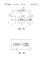
- FIG. 1 ais a block diagram of a processing system incorporating the DRAM cache memory of the present invention
- FIG. 1 bis a diagram of a processing unit incorporating the DRAM cache memory of the present invention
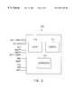
- FIG. 2is a block diagram of the DRAM cache memory
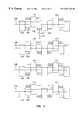
- FIG. 3is a detailed diagram of one embodiment of the memory array in the DRAM cache memory of FIG. 2;
- FIG. 4is a schematic of four global bit lines of the memory array of FIG. 2;
- FIG. 5is a schematic diagram of sense amplifier and I/O devices included in the schematic of FIG. 4;
- FIG. 6is a block diagram of the data path circuitry of the memory of FIG. 2;
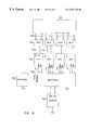
- FIG. 7is a schematic of write circuitry included in the data path circuitry of FIG. 5;
- FIG. 8is a schematic of read circuitry (helper flip/flop) of FIG. 6;
- FIG. 9is a timing diagram of a read operation of the memory of FIG. 2.
- FIG. 10is a timing diagram of a write operation of the memory of FIG. 2 .
- FIG. 1 ais a block diagram of a processing system incorporating the high bandwidth cache memory device of the present invention.
- the systemincludes a central processing unit (CPU) 110 , a main memory 120 , DRAM cache memory 100 , and an optional controller 130 for controlling communication between the CPU and memories.
- the CPUcan communicate with the cache memory, or optionally with the main memory, as indicated by the dashed line.
- typical cache memoriesare SRAM's. SRAM's are faster than typical DRAM's, but have a smaller memory density. That is, a typical DRAM may have 16 Mega bits of memory arranged as 1 Mega bit by 16 bits, while a typical SRAM may have only 128 k bytes of memory arranged as 32 k by 32 bits.
- a DRAM memory having the architecture and data path described hereinwill have high bandwidth, high density, and high operating speeds for use as a cache memory.
- a DRAM cache memorymay have 16 Mega bits of memory arranged as 512 k bits by 32 bits.
- FIG. 1 billustrates an integrated circuit package which includes both a central processing unit and cache DRAM circuitry. The single package processing unit, therefore, reduces the communication time between the processor and the memory circuit. Further, it will be appreciated that the processor and the memory can be incorporated on the same integrated die.
- FIG. 2illustrates a 4 Mega Bit DRAM of the present invention having 64 data input/output connections, or communication lines (DQ 1 -DQ 64 ).
- the memoryis designed to be interchangeable with existing synchronous pipelined SRAM's.
- Control circuitry 141 , memory array 140 , and addressing circuitry 143are provided in the memory.
- the input lines of the DRAMtherefore, correspond to the inputs of the SRAM.
- OE*Output Enable
- BW 1 *-BW 8 *Global Write
- BWE*Block Write Enable
- ClockCLK
- CE*Chip-Enable
- ADV*Synchronous Address Advance
- ADSP*Synchronous Address Status Processor
- ADSC*Synchronous Address Status Controller
- one embodiment of the DRAM of the present inventionhas a memory array 140 arranged in four sub-array sections 142 ( a )-( d ) having memory cells and sense amplifier circuitry.
- the DQ input/outputsare distributed around the memory to reduce the communication time with the array sub-sections.
- Additional circuitry 141 and 143are provided for addressing the memory cells and controlling the operation of the memory as shown in FIG. 2 .
- This additional circuitrycan be located in the gaps 145 between the sub-arrays and around the periphery of array 140 .
- the addressing and control circuitryis not described herein, but known to those skilled in the art.
- Each sub-array sectionhas memory cells arranged in rows and columns of memory cells. Each column is divided into bit line sections which are connected to a sense amplifier circuit. The column sections are arranged in a folded bit line structure to maximize memory cell density.
- FIG. 4shows four columns of sub-array section 142 ( d ) having folded bit lines.
- Each sense amplifier circuit 144has at least one pair of bit lines 146 which can be selectively coupled to one of 256 memory cells 157 by activating access transistor 155 with a corresponding word line 159 . Only one memory cell has been shown in FIG. 4 for simplicity.
- the 4 Meg memory circuit of FIG. 3has five sense amplifier circuits 144 associated with one global bit line pair 148 . Each sense amplifier circuit can couple one of four bit line pairs 146 to the global bit line, as shown in FIG. 4 .
- the global bit lines 148are fabricated parallel to bit lines 146 .
- the global bit linescan be selectively coupled to one of the five sense amplifier circuits 144 .
- a portion of addressing circuitry 143is provided in the gaps 145 to select the appropriate sense amplifier and bit line pair for communication with the global bit line. Another portion of addressing circuitry 143 is also provided to activate a word line 159 to couple a memory cell 157 to a bit line 146 , as known to those skilled in the art.
- the 4 Meg memory circuit of FIG. 2has 256 global bit lines per sub-array section 142 , for a total of 2048 global bit lines. Further, each bit line pair can be coupled to one of 256 memory cells.
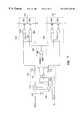
- Each pair of bit lines 146has a dedicated cross coupled pair differential p-sense amplifier circuit 206 which is activated by an appropriate signal on the PSA line. Further, each bit line pair has a dedicated equilibration circuit 208 to equilibrate the bit lines to a predetermined voltage provided on the EQv line. Isolation circuitry 210 is provided to selectively couple one bit line pair to a shared cross coupled pair differential n-sense amplifier circuit 212 . The n-sense amplifier is activated using the NSA line.
- Input/output coupling circuitry 214selectively couples one of the bit line pairs 146 to the global bit lines 148 via communication lines 216 in response to the column select signal (CS). It will be appreciated by those skilled in the art that multiple bit line pairs can be individually coupled to the global bit lines through communication lines 216 and the schematic diagram of FIG. 5 is intended to merely illustrate one embodiment of sense amplifier and coupling circuitry of a memory array.
- the 4 Meg DRAM of FIG. 2has 64 I/O connections, or data communication lines (DQ's). Therefore 16 DQ lines are associated with each array subsection 142 , and can be arranged as shown in FIG. 3 .
- Each DQis associated with 32 global bit line pairs 148 . That is, one of 32 global bit line pairs can be selectively coupled to one DQ line for external data communication though eight-to-one multiplex circuits 165 and a four-to-one multiplex circuit 152 .
- FIG. 6shows 32 pairs of global bit lines 148 of one of the memory sub-array sections 142 connected to four eight-to-one multiplex circuits 165 .
- Each pair of multiplex circuit output lines 151are connected to a helper flip/flop circuit 150 which is connected to multiplex circuit 152 .
- the multiplex circuitin response to counter 154 couples one of the helper flip/flops to a DQ line via buffer 153 .
- the multiplexed global bit line memory architecture of the present inventionallows the memory to be operated in a pipelined synchronous mode suitable for cache applications. It will be understood that any multiplexed architecture can be used in the present invention and will be dependant upon the width (number of DQ lines) and depth (memory cell capacity) of the DRAM.
- FIGS. 7 and 8are schematic diagrams of the write and read circuitry, respectively, generally referred to in combination as helper flip/flop circuits 150 of FIG. 6 .
- FIG. 7is the write circuit which couples multiplexer 152 to multiplex circuit 165 .
- the DQ lineis coupled to the DATA input line 156 .
- Coupling circuit 158receives both DATA and its complement DATA* at nodes 160 and 162 , respectively, and couples the DATA lines to driver circuits 164 and 166 in response to a data latch signal (DL). That is, when DL is high both DATA and DATA* signals are coupled to nodes 168 and 170 .
- DLdata latch signal
- the output of inverter 172is coupled to the input of inverter 174 through latch circuit 176 .
- the output of inverter 174is coupled to the input of inverter 172 through latch circuit 176 .
- the outputs from inverters 172 and 174are coupled to driver circuits 164 and 166 .
- Each driver circuithas a NAND gate 178 , NOR gate 180 , n-channel transistor 182 and a p-channel transistor 184 .
- An inverter 185is also provided between enable circuit 186 and an input to NAND gate 178 .
- the enable circuithas a NAND gate 188 which provides a low output when both the helper flip/flop ENABLE signal is high and an internal Write Enable (WEN) signal is high.
- WENWrite Enable
- the multiplex circuits 165couple communication lines 151 to a selected pair of global bit lines.
- the signal received on a DQ inputis latched and coupled directly to one pair of global bit lines.
- datacan be latched by latch 176 and not provided on communication lines 151 until the ENABLE signal is activated.
- datacan be sequentially latched into the helper flip/flops and all of the helper flip/flops simultaneously coupled to lines, 151 in response to a common ENABLE signal.
- the read operation circuitryuses a latch to hold data from the communication lines 151 until multiplexer circuit 152 couples the flip/flop circuit to the associated DQ line.
- Equilibrate circuit 190equilibrates the communication lines 151 to a predetermined voltage such as Vcc/2 when equilibrate signal (EQ) is high.
- transistor 192equilibrates nodes 194 and 196 while the helper flip/flop enable signal (HFF) is low.
- Isolation devices 198isolate the communication lines from nodes 194 and 196 in response to isolation signal (ISO).
- Amplifier latch circuit 200drives nodes 194 and 196 to appropriate power rails in response to a high HFF signal.
- driver circuits 202drive the DR and DR* lines to the appropriate power rail in response to HFF, node 194 and node 196 .
- Any sense and amplify circuitcan be used as latch 200 , therefore, the present invention is not limited to the cross-coupled circuit shown.
- FIGS. 9 and 10illustrate timing diagrams for synchronous pipelined read and write operations of the cache DRAM.
- a memory address(ADD 1 ) is received from the memory address inputs on an active transition of the clock signal (high transition) at time t1.
- CE*Chip Enable
- ADSP*Synchronous Address Status Processor
- CE*Chip Enable
- ADSP*Synchronous Address Status Processor
- ADSC*Synchronous Address Status Control
- This datacorresponds to memory address ADD 1 and helper flip/flop 1 .
- Subsequent active cycles of the clock(t3-t5) will output data latched in helper flip/flops 2 - 4 (shown as DATA 12 -DATA 14 ).
- a new external address(ADD 2 ) is registered on the fifth clock cycle (t5) and data DATA 21 - 24 is output on the DQ lines starting at time t6.
- ADSP signalis received early in the output sequence, the data from additional helper flip/flops is terminated. This is illustrated by the absence of DATA 32 - 34 during the third output sequence in response to the ADSP signal received at time t11. It will be understood that by multiplexing the flip/flops the DRAM of the present invention can output data on each clock cycle, thereby, eliminating the need for latency between output data.
- a clock latencyis provided, however, following both the initial address and termination of an output sequence.
- a synchronous write operationis initiated on an active transition of the clock when a write enable signal (W*) is active.
- W*write enable signal
- a new memory addressis latched when both CE* and ADSP* are low.
- the cache DRAMmust accept either a single write operation or a burst operation. That is, data will either be written to the memory array in a single write operation to a designated address provided on the address lines, or be written to the memory in a burst operation to a predetermined sequence of memory addresses starting at a designated address provided on the address lines.
- the DRAM cache memoryopens and closes a page of the memory array to allow the memory to operate in a pipelined manner.
- the appropriate memory array pageis opened by controller circuit 141 , FIG. 2 .
- the write enable signal (W*) provided at time t2indicates that a write operation is to be performed. At this time, the memory does not know what type of write operation is to be performed, single or burst.
- the data provided on the DQ linesis latched in a helper flip/flop and then written to the memory array page, as described above with reference to FIG. 7 .
- the controller 141closes the accessed page prior to time t3.
- the pageis re-opened and the burst write operation is continued by latching the data and then writing the latched data to the memory array, as shown in FIG. 10 .
- the pageis closed in preparation of a new address at time t5.
- ADSP*new address alert
- a dynamic memory devicewhich includes multiplexed global bit lines.
- Memory cellscan be selectively coupled to the global bit lines, and a group of global bit lines are multiplexed to data communication connections (DQ lines).
- DQ linesdata communication connections
- the multiplexed architectureallows the DRAM to read and write data at speeds needed to function as cache memory.
- any size memory arraycan be used, including 256 k, 1 meg, 2 meg, 4 meg, 8 meg and 16 meg, and any number of DQ lines can be used, including 4, 8, 16, 32 and 64. Therefore, it is manifestly intended that this invention be limited only by the claims and the equivalents thereof.
Landscapes
- Dram (AREA)
Abstract
Description
Claims (42)
Priority Applications (1)
| Application Number | Priority Date | Filing Date | Title |
|---|---|---|---|
| US09/291,536US6201740B1 (en) | 1997-02-26 | 1999-04-14 | Cache memories using DRAM cells with high-speed data path |
Applications Claiming Priority (3)
| Application Number | Priority Date | Filing Date | Title |
|---|---|---|---|
| US08/806,206US5801996A (en) | 1997-02-26 | 1997-02-26 | Data path for high speed high bandwidth DRAM |
| US09/109,951US5933372A (en) | 1997-02-26 | 1998-07-02 | Data path for high speed high bandwidth DRAM |
| US09/291,536US6201740B1 (en) | 1997-02-26 | 1999-04-14 | Cache memories using DRAM cells with high-speed data path |
Related Parent Applications (1)
| Application Number | Title | Priority Date | Filing Date |
|---|---|---|---|
| US09/109,951ContinuationUS5933372A (en) | 1997-02-26 | 1998-07-02 | Data path for high speed high bandwidth DRAM |
Publications (1)
| Publication Number | Publication Date |
|---|---|
| US6201740B1true US6201740B1 (en) | 2001-03-13 |
Family
ID=25193567
Family Applications (3)
| Application Number | Title | Priority Date | Filing Date |
|---|---|---|---|
| US08/806,206Expired - LifetimeUS5801996A (en) | 1997-02-26 | 1997-02-26 | Data path for high speed high bandwidth DRAM |
| US09/109,951Expired - LifetimeUS5933372A (en) | 1997-02-26 | 1998-07-02 | Data path for high speed high bandwidth DRAM |
| US09/291,536Expired - LifetimeUS6201740B1 (en) | 1997-02-26 | 1999-04-14 | Cache memories using DRAM cells with high-speed data path |
Family Applications Before (2)
| Application Number | Title | Priority Date | Filing Date |
|---|---|---|---|
| US08/806,206Expired - LifetimeUS5801996A (en) | 1997-02-26 | 1997-02-26 | Data path for high speed high bandwidth DRAM |
| US09/109,951Expired - LifetimeUS5933372A (en) | 1997-02-26 | 1998-07-02 | Data path for high speed high bandwidth DRAM |
Country Status (1)
| Country | Link |
|---|---|
| US (3) | US5801996A (en) |
Cited By (8)
| Publication number | Priority date | Publication date | Assignee | Title |
|---|---|---|---|---|
| US6415370B1 (en)* | 1998-09-08 | 2002-07-02 | Fujitsu Limited | Semiconductor integrated circuit |
| US7047385B1 (en)* | 2003-06-16 | 2006-05-16 | Cisco Technology, Inc. | High-speed memory for use in networking systems |
| US7123521B1 (en) | 2005-04-27 | 2006-10-17 | Micron Technology, Inc. | Random cache read |
| EP1497733A4 (en)* | 2002-04-25 | 2008-04-30 | Ibm | Destructive-read random access memory system buffered with destructive-read memory cache |
| US20080181021A1 (en)* | 2007-01-26 | 2008-07-31 | Thayer Larry J | Memory module and method employing a multiplexer to replace a memory device |
| US20090196086A1 (en)* | 2008-02-05 | 2009-08-06 | Pelley Perry H | High bandwidth cache-to-processing unit communication in a multiple processor/cache system |
| US20140281130A1 (en)* | 2013-03-15 | 2014-09-18 | The Boeing Company | Accessing non-volatile memory through a volatile shadow memory |
| US9697145B2 (en)* | 2015-06-12 | 2017-07-04 | Apple Inc. | Memory interface system |
Families Citing this family (5)
| Publication number | Priority date | Publication date | Assignee | Title |
|---|---|---|---|---|
| US6081872A (en)* | 1997-07-07 | 2000-06-27 | International Business Machines Corporation | Cache reloading performance improvement through the use of early select techniques with and without pipelining |
| US6044432A (en)* | 1997-11-12 | 2000-03-28 | Vlsi Technology, Inc. | Method and system for latching an address for accessing synchronous random access memory using a single address status signal control line |
| US6473838B1 (en) | 2000-01-04 | 2002-10-29 | International Business Machines Corporation | Data transfer system for multiple network processors using dual DRAM storage |
| US6396728B1 (en) | 2000-07-28 | 2002-05-28 | Micron Technology, Inc. | Array organization for high-performance memory devices |
| US6549471B1 (en) | 2002-02-11 | 2003-04-15 | Micron Technology, Inc. | Adiabatic differential driver |
Citations (4)
| Publication number | Priority date | Publication date | Assignee | Title |
|---|---|---|---|---|
| US4303986A (en) | 1979-01-09 | 1981-12-01 | Hakan Lans | Data processing system and apparatus for color graphics display |
| US5666312A (en) | 1994-11-23 | 1997-09-09 | Sony Corporation Of Japan | Column redundancy scheme for a random access memory incorporating multiplexers and demultiplexers for replacing defective columns in any memory array |
| US5831924A (en)* | 1995-09-07 | 1998-11-03 | Mitsubishi Denki Kabushiki Kaisha | Synchronous semiconductor memory device having a plurality of banks distributed in a plurality of memory arrays |
| US6006309A (en)* | 1996-12-16 | 1999-12-21 | Bull Hn Information Systems Inc. | Information block transfer management in a multiprocessor computer system employing private caches for individual center processor units and a shared cache |
- 1997
- 1997-02-26USUS08/806,206patent/US5801996A/ennot_activeExpired - Lifetime
- 1998
- 1998-07-02USUS09/109,951patent/US5933372A/ennot_activeExpired - Lifetime
- 1999
- 1999-04-14USUS09/291,536patent/US6201740B1/ennot_activeExpired - Lifetime
Patent Citations (4)
| Publication number | Priority date | Publication date | Assignee | Title |
|---|---|---|---|---|
| US4303986A (en) | 1979-01-09 | 1981-12-01 | Hakan Lans | Data processing system and apparatus for color graphics display |
| US5666312A (en) | 1994-11-23 | 1997-09-09 | Sony Corporation Of Japan | Column redundancy scheme for a random access memory incorporating multiplexers and demultiplexers for replacing defective columns in any memory array |
| US5831924A (en)* | 1995-09-07 | 1998-11-03 | Mitsubishi Denki Kabushiki Kaisha | Synchronous semiconductor memory device having a plurality of banks distributed in a plurality of memory arrays |
| US6006309A (en)* | 1996-12-16 | 1999-12-21 | Bull Hn Information Systems Inc. | Information block transfer management in a multiprocessor computer system employing private caches for individual center processor units and a shared cache |
Cited By (14)
| Publication number | Priority date | Publication date | Assignee | Title |
|---|---|---|---|---|
| US6415370B1 (en)* | 1998-09-08 | 2002-07-02 | Fujitsu Limited | Semiconductor integrated circuit |
| EP1497733A4 (en)* | 2002-04-25 | 2008-04-30 | Ibm | Destructive-read random access memory system buffered with destructive-read memory cache |
| US7047385B1 (en)* | 2003-06-16 | 2006-05-16 | Cisco Technology, Inc. | High-speed memory for use in networking systems |
| US7369447B2 (en) | 2005-04-27 | 2008-05-06 | Micron Technology, Inc. | Random cache read |
| US20080074933A1 (en)* | 2005-04-27 | 2008-03-27 | Micron Technology, Inc. | Random cache read |
| US20060245270A1 (en)* | 2005-04-27 | 2006-11-02 | Micron Technology, Inc. | Random cache read |
| US7123521B1 (en) | 2005-04-27 | 2006-10-17 | Micron Technology, Inc. | Random cache read |
| US20080181021A1 (en)* | 2007-01-26 | 2008-07-31 | Thayer Larry J | Memory module and method employing a multiplexer to replace a memory device |
| US8886892B2 (en)* | 2007-01-26 | 2014-11-11 | Hewlett-Packard Development Company, L.P. | Memory module and method employing a multiplexer to replace a memory device |
| US20090196086A1 (en)* | 2008-02-05 | 2009-08-06 | Pelley Perry H | High bandwidth cache-to-processing unit communication in a multiple processor/cache system |
| US7777330B2 (en)* | 2008-02-05 | 2010-08-17 | Freescale Semiconductor, Inc. | High bandwidth cache-to-processing unit communication in a multiple processor/cache system |
| US20140281130A1 (en)* | 2013-03-15 | 2014-09-18 | The Boeing Company | Accessing non-volatile memory through a volatile shadow memory |
| US10089224B2 (en)* | 2013-03-15 | 2018-10-02 | The Boeing Company | Write caching using volatile shadow memory |
| US9697145B2 (en)* | 2015-06-12 | 2017-07-04 | Apple Inc. | Memory interface system |
Also Published As
| Publication number | Publication date |
|---|---|
| US5933372A (en) | 1999-08-03 |
| US5801996A (en) | 1998-09-01 |
Similar Documents
| Publication | Publication Date | Title |
|---|---|---|
| US6510492B2 (en) | Apparatus for controlling data transfer between a bus and memory array and method for operating same | |
| CN1307647C (en) | Dynamic random access memory, memory device and method for executing read command | |
| US6105106A (en) | Computer system, memory device and shift register including a balanced switching circuit with series connected transfer gates which are selectively clocked for fast switching times | |
| EP0639835B1 (en) | Dynamic random access memory device with sense amplifiers serving as cache memory independent of row address buffer unit for high-speed sequential access | |
| US6359813B1 (en) | Semiconductor memory device having improved data transfer rate without providing a register for holding write data | |
| JP4370507B2 (en) | Semiconductor integrated circuit device | |
| EP0895162A2 (en) | Enhanced dram with embedded registers | |
| US20090083479A1 (en) | Multiport semiconductor memory device and associated refresh method | |
| US6201740B1 (en) | Cache memories using DRAM cells with high-speed data path | |
| US6445632B2 (en) | Semiconductor memory device for fast access | |
| US6320816B2 (en) | Column select latch for SDRAM | |
| US20040047221A1 (en) | Semiconductor memory device requiring refresh operation | |
| US6205069B1 (en) | Semiconductor memory device with fast input/output line precharge scheme and method of precharging input/output lines thereof | |
| US5963493A (en) | Memory device communication line control | |
| JPH0887887A (en) | Semiconductor memory device | |
| US6501698B1 (en) | Structure and method for hiding DRAM cycle time behind a burst access | |
| KR100498466B1 (en) | 4Bit prefetch type FCRAM having the improved control circuit for writing data in memory cell array and data masking method thereof | |
| US6345007B1 (en) | Prefetch and restore method and apparatus of semiconductor memory device | |
| JPH0520834B2 (en) | ||
| US6023428A (en) | Integrated circuit device having a memory array with segmented bit lines and method of operation | |
| US6219283B1 (en) | Memory device with local write data latches | |
| US6288952B1 (en) | System for improved memory cell access | |
| US6044433A (en) | DRAM cache | |
| JPH08297969A (en) | Dynamic semiconductor memory device | |
| US6859400B2 (en) | Semiconductor memory device |
Legal Events
| Date | Code | Title | Description |
|---|---|---|---|
| FEPP | Fee payment procedure | Free format text:PAYOR NUMBER ASSIGNED (ORIGINAL EVENT CODE: ASPN); ENTITY STATUS OF PATENT OWNER: LARGE ENTITY | |
| STCF | Information on status: patent grant | Free format text:PATENTED CASE | |
| CC | Certificate of correction | ||
| FPAY | Fee payment | Year of fee payment:4 | |
| FPAY | Fee payment | Year of fee payment:8 | |
| FPAY | Fee payment | Year of fee payment:12 | |
| AS | Assignment | Owner name:U.S. BANK NATIONAL ASSOCIATION, AS COLLATERAL AGENT, CALIFORNIA Free format text:SECURITY INTEREST;ASSIGNOR:MICRON TECHNOLOGY, INC.;REEL/FRAME:038669/0001 Effective date:20160426 Owner name:U.S. BANK NATIONAL ASSOCIATION, AS COLLATERAL AGEN Free format text:SECURITY INTEREST;ASSIGNOR:MICRON TECHNOLOGY, INC.;REEL/FRAME:038669/0001 Effective date:20160426 | |
| AS | Assignment | Owner name:MORGAN STANLEY SENIOR FUNDING, INC., AS COLLATERAL AGENT, MARYLAND Free format text:PATENT SECURITY AGREEMENT;ASSIGNOR:MICRON TECHNOLOGY, INC.;REEL/FRAME:038954/0001 Effective date:20160426 Owner name:MORGAN STANLEY SENIOR FUNDING, INC., AS COLLATERAL Free format text:PATENT SECURITY AGREEMENT;ASSIGNOR:MICRON TECHNOLOGY, INC.;REEL/FRAME:038954/0001 Effective date:20160426 | |
| AS | Assignment | Owner name:U.S. BANK NATIONAL ASSOCIATION, AS COLLATERAL AGENT, CALIFORNIA Free format text:CORRECTIVE ASSIGNMENT TO CORRECT THE REPLACE ERRONEOUSLY FILED PATENT #7358718 WITH THE CORRECT PATENT #7358178 PREVIOUSLY RECORDED ON REEL 038669 FRAME 0001. ASSIGNOR(S) HEREBY CONFIRMS THE SECURITY INTEREST;ASSIGNOR:MICRON TECHNOLOGY, INC.;REEL/FRAME:043079/0001 Effective date:20160426 Owner name:U.S. BANK NATIONAL ASSOCIATION, AS COLLATERAL AGEN Free format text:CORRECTIVE ASSIGNMENT TO CORRECT THE REPLACE ERRONEOUSLY FILED PATENT #7358718 WITH THE CORRECT PATENT #7358178 PREVIOUSLY RECORDED ON REEL 038669 FRAME 0001. ASSIGNOR(S) HEREBY CONFIRMS THE SECURITY INTEREST;ASSIGNOR:MICRON TECHNOLOGY, INC.;REEL/FRAME:043079/0001 Effective date:20160426 | |
| AS | Assignment | Owner name:MICRON TECHNOLOGY, INC., IDAHO Free format text:RELEASE BY SECURED PARTY;ASSIGNOR:U.S. BANK NATIONAL ASSOCIATION, AS COLLATERAL AGENT;REEL/FRAME:047243/0001 Effective date:20180629 | |
| AS | Assignment | Owner name:MICRON TECHNOLOGY, INC., IDAHO Free format text:RELEASE BY SECURED PARTY;ASSIGNOR:MORGAN STANLEY SENIOR FUNDING, INC., AS COLLATERAL AGENT;REEL/FRAME:050937/0001 Effective date:20190731 |