US6201701B1 - Integrated substrate with enhanced thermal characteristics - Google Patents
Integrated substrate with enhanced thermal characteristicsDownload PDFInfo
- Publication number
- US6201701B1 US6201701B1US09/038,118US3811898AUS6201701B1US 6201701 B1US6201701 B1US 6201701B1US 3811898 AUS3811898 AUS 3811898AUS 6201701 B1US6201701 B1US 6201701B1
- Authority
- US
- United States
- Prior art keywords
- circuit board
- substrate
- layer
- base
- pattern
- Prior art date
- Legal status (The legal status is an assumption and is not a legal conclusion. Google has not performed a legal analysis and makes no representation as to the accuracy of the status listed.)
- Expired - Fee Related
Links
- 239000000758substrateSubstances0.000titleclaimsabstractdescription144
- 239000000463materialSubstances0.000claimsabstractdescription105
- 239000011888foilSubstances0.000claimsabstractdescription70
- 239000004065semiconductorSubstances0.000claimsabstractdescription69
- RYGMFSIKBFXOCR-UHFFFAOYSA-NCopperChemical compound[Cu]RYGMFSIKBFXOCR-UHFFFAOYSA-N0.000claimsdescription114
- 229910052782aluminiumInorganic materials0.000claimsdescription43
- XAGFODPZIPBFFR-UHFFFAOYSA-NaluminiumChemical compound[Al]XAGFODPZIPBFFR-UHFFFAOYSA-N0.000claimsdescription43
- 239000011889copper foilSubstances0.000claimsdescription35
- 229910052802copperInorganic materials0.000claimsdescription26
- 239000010949copperSubstances0.000claimsdescription26
- 238000012546transferMethods0.000claimsdescription4
- 229910052582BNInorganic materials0.000claimsdescription3
- PZNSFCLAULLKQX-UHFFFAOYSA-NBoron nitrideChemical compoundN#BPZNSFCLAULLKQX-UHFFFAOYSA-N0.000claimsdescription3
- 239000004593EpoxySubstances0.000claimsdescription3
- 239000000945fillerSubstances0.000claimsdescription3
- 229920001187thermosetting polymerPolymers0.000claimsdescription3
- 239000010410layerSubstances0.000description105
- 239000011162core materialSubstances0.000description18
- 230000008901benefitEffects0.000description16
- 238000013461designMethods0.000description14
- 238000004519manufacturing processMethods0.000description11
- 229910052751metalInorganic materials0.000description10
- 239000002184metalSubstances0.000description10
- 238000000034methodMethods0.000description10
- 239000000919ceramicSubstances0.000description9
- 238000003475laminationMethods0.000description7
- 239000004020conductorSubstances0.000description6
- 230000005611electricityEffects0.000description6
- 239000003990capacitorSubstances0.000description5
- 230000001965increasing effectEffects0.000description5
- PNEYBMLMFCGWSK-UHFFFAOYSA-NAluminaChemical compound[O-2].[O-2].[O-2].[Al+3].[Al+3]PNEYBMLMFCGWSK-UHFFFAOYSA-N0.000description4
- 238000005516engineering processMethods0.000description4
- 230000017525heat dissipationEffects0.000description4
- PMHQVHHXPFUNSP-UHFFFAOYSA-Mcopper(1+);methylsulfanylmethane;bromideChemical compoundBr[Cu].CSCPMHQVHHXPFUNSP-UHFFFAOYSA-M0.000description3
- 239000000203mixtureSubstances0.000description3
- PXHVJJICTQNCMI-UHFFFAOYSA-NNickelChemical compound[Ni]PXHVJJICTQNCMI-UHFFFAOYSA-N0.000description2
- 238000013459approachMethods0.000description2
- 229910010293ceramic materialInorganic materials0.000description2
- 230000003247decreasing effectEffects0.000description2
- 238000011161developmentMethods0.000description2
- 230000018109developmental processEffects0.000description2
- -1howeverSubstances0.000description2
- 238000010030laminatingMethods0.000description2
- 229910001218Gallium arsenideInorganic materials0.000description1
- 230000006978adaptationEffects0.000description1
- 230000015572biosynthetic processEffects0.000description1
- 150000001875compoundsChemical class0.000description1
- 230000001419dependent effectEffects0.000description1
- 238000010586diagramMethods0.000description1
- 230000000694effectsEffects0.000description1
- 230000002708enhancing effectEffects0.000description1
- 230000007613environmental effectEffects0.000description1
- 238000005530etchingMethods0.000description1
- RTZKZFJDLAIYFH-UHFFFAOYSA-NetherSubstancesCCOCCRTZKZFJDLAIYFH-UHFFFAOYSA-N0.000description1
- 125000001033ether groupChemical group0.000description1
- 239000011521glassSubstances0.000description1
- PCHJSUWPFVWCPO-UHFFFAOYSA-NgoldChemical compound[Au]PCHJSUWPFVWCPO-UHFFFAOYSA-N0.000description1
- 239000010931goldSubstances0.000description1
- 229910052737goldInorganic materials0.000description1
- 238000010438heat treatmentMethods0.000description1
- 239000012535impuritySubstances0.000description1
- 150000002739metalsChemical class0.000description1
- 238000000465mouldingMethods0.000description1
- 229910052759nickelInorganic materials0.000description1
- 238000013021overheatingMethods0.000description1
- TWNQGVIAIRXVLR-UHFFFAOYSA-Noxo(oxoalumanyloxy)alumaneChemical compoundO=[Al]O[Al]=OTWNQGVIAIRXVLR-UHFFFAOYSA-N0.000description1
- 239000011347resinSubstances0.000description1
- 229920005989resinPolymers0.000description1
- 239000002356single layerSubstances0.000description1
- 229910000679solderInorganic materials0.000description1
- 239000002699waste materialSubstances0.000description1
Images


Classifications
- H—ELECTRICITY
- H05—ELECTRIC TECHNIQUES NOT OTHERWISE PROVIDED FOR
- H05K—PRINTED CIRCUITS; CASINGS OR CONSTRUCTIONAL DETAILS OF ELECTRIC APPARATUS; MANUFACTURE OF ASSEMBLAGES OF ELECTRICAL COMPONENTS
- H05K1/00—Printed circuits
- H05K1/02—Details
- H05K1/0201—Thermal arrangements, e.g. for cooling, heating or preventing overheating
- H05K1/0203—Cooling of mounted components
- H05K1/021—Components thermally connected to metal substrates or heat-sinks by insert mounting
- H—ELECTRICITY
- H05—ELECTRIC TECHNIQUES NOT OTHERWISE PROVIDED FOR
- H05K—PRINTED CIRCUITS; CASINGS OR CONSTRUCTIONAL DETAILS OF ELECTRIC APPARATUS; MANUFACTURE OF ASSEMBLAGES OF ELECTRICAL COMPONENTS
- H05K1/00—Printed circuits
- H05K1/02—Details
- H05K1/0201—Thermal arrangements, e.g. for cooling, heating or preventing overheating
- H05K1/0203—Cooling of mounted components
- H05K1/0204—Cooling of mounted components using means for thermal conduction connection in the thickness direction of the substrate
- H05K1/0206—Cooling of mounted components using means for thermal conduction connection in the thickness direction of the substrate by printed thermal vias
- H—ELECTRICITY
- H01—ELECTRIC ELEMENTS
- H01L—SEMICONDUCTOR DEVICES NOT COVERED BY CLASS H10
- H01L2224/00—Indexing scheme for arrangements for connecting or disconnecting semiconductor or solid-state bodies and methods related thereto as covered by H01L24/00
- H01L2224/01—Means for bonding being attached to, or being formed on, the surface to be connected, e.g. chip-to-package, die-attach, "first-level" interconnects; Manufacturing methods related thereto
- H01L2224/42—Wire connectors; Manufacturing methods related thereto
- H01L2224/47—Structure, shape, material or disposition of the wire connectors after the connecting process
- H01L2224/48—Structure, shape, material or disposition of the wire connectors after the connecting process of an individual wire connector
- H01L2224/4805—Shape
- H01L2224/4809—Loop shape
- H01L2224/48091—Arched
- H—ELECTRICITY
- H01—ELECTRIC ELEMENTS
- H01L—SEMICONDUCTOR DEVICES NOT COVERED BY CLASS H10
- H01L2224/00—Indexing scheme for arrangements for connecting or disconnecting semiconductor or solid-state bodies and methods related thereto as covered by H01L24/00
- H01L2224/01—Means for bonding being attached to, or being formed on, the surface to be connected, e.g. chip-to-package, die-attach, "first-level" interconnects; Manufacturing methods related thereto
- H01L2224/42—Wire connectors; Manufacturing methods related thereto
- H01L2224/47—Structure, shape, material or disposition of the wire connectors after the connecting process
- H01L2224/48—Structure, shape, material or disposition of the wire connectors after the connecting process of an individual wire connector
- H01L2224/481—Disposition
- H01L2224/48151—Connecting between a semiconductor or solid-state body and an item not being a semiconductor or solid-state body, e.g. chip-to-substrate, chip-to-passive
- H01L2224/48221—Connecting between a semiconductor or solid-state body and an item not being a semiconductor or solid-state body, e.g. chip-to-substrate, chip-to-passive the body and the item being stacked
- H01L2224/48225—Connecting between a semiconductor or solid-state body and an item not being a semiconductor or solid-state body, e.g. chip-to-substrate, chip-to-passive the body and the item being stacked the item being non-metallic, e.g. insulating substrate with or without metallisation
- H01L2224/48227—Connecting between a semiconductor or solid-state body and an item not being a semiconductor or solid-state body, e.g. chip-to-substrate, chip-to-passive the body and the item being stacked the item being non-metallic, e.g. insulating substrate with or without metallisation connecting the wire to a bond pad of the item
- H—ELECTRICITY
- H01—ELECTRIC ELEMENTS
- H01L—SEMICONDUCTOR DEVICES NOT COVERED BY CLASS H10
- H01L2224/00—Indexing scheme for arrangements for connecting or disconnecting semiconductor or solid-state bodies and methods related thereto as covered by H01L24/00
- H01L2224/01—Means for bonding being attached to, or being formed on, the surface to be connected, e.g. chip-to-package, die-attach, "first-level" interconnects; Manufacturing methods related thereto
- H01L2224/42—Wire connectors; Manufacturing methods related thereto
- H01L2224/47—Structure, shape, material or disposition of the wire connectors after the connecting process
- H01L2224/48—Structure, shape, material or disposition of the wire connectors after the connecting process of an individual wire connector
- H01L2224/484—Connecting portions
- H01L2224/4847—Connecting portions the connecting portion on the bonding area of the semiconductor or solid-state body being a wedge bond
- H01L2224/48472—Connecting portions the connecting portion on the bonding area of the semiconductor or solid-state body being a wedge bond the other connecting portion not on the bonding area also being a wedge bond, i.e. wedge-to-wedge
- H—ELECTRICITY
- H01—ELECTRIC ELEMENTS
- H01L—SEMICONDUCTOR DEVICES NOT COVERED BY CLASS H10
- H01L2924/00—Indexing scheme for arrangements or methods for connecting or disconnecting semiconductor or solid-state bodies as covered by H01L24/00
- H01L2924/10—Details of semiconductor or other solid state devices to be connected
- H01L2924/11—Device type
- H01L2924/13—Discrete devices, e.g. 3 terminal devices
- H01L2924/1301—Thyristor
- H01L2924/13033—TRIAC - Triode for Alternating Current - A bidirectional switching device containing two thyristor structures with common gate contact
- H—ELECTRICITY
- H01—ELECTRIC ELEMENTS
- H01L—SEMICONDUCTOR DEVICES NOT COVERED BY CLASS H10
- H01L2924/00—Indexing scheme for arrangements or methods for connecting or disconnecting semiconductor or solid-state bodies as covered by H01L24/00
- H01L2924/10—Details of semiconductor or other solid state devices to be connected
- H01L2924/11—Device type
- H01L2924/13—Discrete devices, e.g. 3 terminal devices
- H01L2924/1304—Transistor
- H01L2924/1305—Bipolar Junction Transistor [BJT]
- H01L2924/13055—Insulated gate bipolar transistor [IGBT]
- H—ELECTRICITY
- H01—ELECTRIC ELEMENTS
- H01L—SEMICONDUCTOR DEVICES NOT COVERED BY CLASS H10
- H01L2924/00—Indexing scheme for arrangements or methods for connecting or disconnecting semiconductor or solid-state bodies as covered by H01L24/00
- H01L2924/10—Details of semiconductor or other solid state devices to be connected
- H01L2924/11—Device type
- H01L2924/13—Discrete devices, e.g. 3 terminal devices
- H01L2924/1304—Transistor
- H01L2924/1306—Field-effect transistor [FET]
- H01L2924/13091—Metal-Oxide-Semiconductor Field-Effect Transistor [MOSFET]
- H—ELECTRICITY
- H05—ELECTRIC TECHNIQUES NOT OTHERWISE PROVIDED FOR
- H05K—PRINTED CIRCUITS; CASINGS OR CONSTRUCTIONAL DETAILS OF ELECTRIC APPARATUS; MANUFACTURE OF ASSEMBLAGES OF ELECTRICAL COMPONENTS
- H05K1/00—Printed circuits
- H05K1/18—Printed circuits structurally associated with non-printed electric components
- H05K1/182—Printed circuits structurally associated with non-printed electric components associated with components mounted in the printed circuit board, e.g. insert mounted components [IMC]
- H05K1/183—Components mounted in and supported by recessed areas of the printed circuit board
- H—ELECTRICITY
- H05—ELECTRIC TECHNIQUES NOT OTHERWISE PROVIDED FOR
- H05K—PRINTED CIRCUITS; CASINGS OR CONSTRUCTIONAL DETAILS OF ELECTRIC APPARATUS; MANUFACTURE OF ASSEMBLAGES OF ELECTRICAL COMPONENTS
- H05K2201/00—Indexing scheme relating to printed circuits covered by H05K1/00
- H05K2201/10—Details of components or other objects attached to or integrated in a printed circuit board
- H05K2201/10007—Types of components
- H05K2201/10166—Transistor
- H—ELECTRICITY
- H05—ELECTRIC TECHNIQUES NOT OTHERWISE PROVIDED FOR
- H05K—PRINTED CIRCUITS; CASINGS OR CONSTRUCTIONAL DETAILS OF ELECTRIC APPARATUS; MANUFACTURE OF ASSEMBLAGES OF ELECTRICAL COMPONENTS
- H05K3/00—Apparatus or processes for manufacturing printed circuits
- H05K3/0058—Laminating printed circuit boards onto other substrates, e.g. metallic substrates
- H05K3/0061—Laminating printed circuit boards onto other substrates, e.g. metallic substrates onto a metallic substrate, e.g. a heat sink
- H—ELECTRICITY
- H05—ELECTRIC TECHNIQUES NOT OTHERWISE PROVIDED FOR
- H05K—PRINTED CIRCUITS; CASINGS OR CONSTRUCTIONAL DETAILS OF ELECTRIC APPARATUS; MANUFACTURE OF ASSEMBLAGES OF ELECTRICAL COMPONENTS
- H05K3/00—Apparatus or processes for manufacturing printed circuits
- H05K3/40—Forming printed elements for providing electric connections to or between printed circuits
- H05K3/42—Plated through-holes or plated via connections
- H05K3/429—Plated through-holes specially for multilayer circuits, e.g. having connections to inner circuit layers
- H—ELECTRICITY
- H05—ELECTRIC TECHNIQUES NOT OTHERWISE PROVIDED FOR
- H05K—PRINTED CIRCUITS; CASINGS OR CONSTRUCTIONAL DETAILS OF ELECTRIC APPARATUS; MANUFACTURE OF ASSEMBLAGES OF ELECTRICAL COMPONENTS
- H05K3/00—Apparatus or processes for manufacturing printed circuits
- H05K3/46—Manufacturing multilayer circuits
- H05K3/4611—Manufacturing multilayer circuits by laminating two or more circuit boards
- H05K3/4641—Manufacturing multilayer circuits by laminating two or more circuit boards having integrally laminated metal sheets or special power cores
Definitions
- the present inventiongenerally relates to substrates which interconnect and dissipate heat from power semiconductor elements and more particularly to integrated substrates having enhanced thermal characteristics in which interconnecting wiring patterns for power and control circuit elements are combined.
- aluminaaluminum oxide
- aluminum nitride ceramic substrateusing an oxide interface.
- the thin copper layeris then electroplated to increase its thickness to greater than 0.005 inches.
- the substrateis then used to interconnect high current devices.
- current carrying capabilityis a direct function of cross-sectional area and a high current device therefore requires either a wider or a thicker conductor to have sufficient cross-sectional area.
- alumina or aluminum nitride ceramic substrates which use 0.005 inch thick copperis that these modules are not able to carry high currents without requiring a larger surface area on the module, thereby unsuitably increasing the overall size of the module.
- alumina or aluminum nitride ceramic substrate technologyinclude chemically bonding thicker copper foils, greater than 0.005 inches, to a ceramic substrate. Even with a thicker foil, however, ceramic based substrates have drawbacks. A ceramic based substrate generally must be mounted on a structural base, otherwise the brittle ceramic material can break. In most applications, size of the circuit is an important consideration, and it is undesirable to waste valuable space with the additional structural base required to support the ceramic substrate. Furthermore, even in applications where a structural base can be avoided, the brittle ceramic substrates require special fasteners to avoid breakage.
- U.S. Pat. No. 5,513,072involves a common module containing a power semiconductor element, a circuit board for the power element, a circuit board for a control circuit and a heat spreader fixed on a metal plate.
- the power elementis mounted onto the heat spreader, which is formed as a copper or copper clad island.
- the heat spreaderis adhered to the metal plate by a high heat radiating insulating layer made of resin based material so that the heat spreader and the metal plate are electrically insulated from each other.
- the wiring pattern for the power semiconductor elementis formed in a power circuit control board disposed adjacent to one side of the power element on the metal plate. Attached to the metal plate and placed on the opposite side of the power semiconductor is an additional circuit board which is used for wiring control circuitry.
- a power module as disclosed by U.S. Pat. No. 5,513,072includes high and low power devices on one base plate, but suffers drawbacks.
- the wiring pattern for the power semiconductorcannot be placed beneath the power semiconductor in such a design. Instead, a power circuit board is placed adjacent to the power element, thereby using more valuable space on the module.
- a design allowing the power element wiring pattern to be placed intermediate the power semiconductor element and the metal platewould save valuable space and achieve a smaller module.
- the designrequires a separate heat spreader positioned between the power element and the metal base in order to dissipate heat. A thinner, cheaper module could be constructed if the heat spreader could be eliminated.
- 5,513,072requires two separate circuit boards, one of which is for interconnecting high power elements while the other circuit board connects the low power circuitry.
- a power module having two instead of one circuit boardadds a step to the manufacturing process, in turn increasing cost.
- a power module having two circuit boardsrequires a larger design than a power module with one circuit board.
- One known deviceis an automotive power steering module that utilizes a large (8 inches by 4 inches) copper interconnect pattern bonded to an aluminum substrate.
- the interconnect patternis approximately 0.020 inch thick and interconnects large power semiconductors and switches currents greater than 75 amperes.
- the aluminum baseserves not only as the mounting platform for the semiconductors but is also an integral part of the system, serving as a structural mounting member in the power steering assembly.
- a low power interconnect using a single layer printed circuit boardis bonded to the thick copper foil and provides control signal connections.
- a power module for a surgical sawis a known product.
- a copper interconnect pattern having a thickness greater than 0.010 inchesis again bonded to an aluminum substrate and is used to interconnect the switching power transistors that control the brushless motor in the surgical saw.
- the sawfeatures a high torque which requires switching of currents greater than 30 amperes by the power module.
- ABS systemautomotive anti-lock braking system
- This known modulealso utilizes a thick copper interconnect pattern bonded to an aluminum substrate to interconnect power transistors and to switch the large currents required in the ABS system.
- the module for the automotive ABS systemalso is formed as an integral part of the system, thereby giving structural strength to the overall assembly.
- the present inventionovercomes the disadvantages of the above described prior art by providing a thermally efficient multi-layered integrated substrate having wiring patterns for both power semiconductor elements and control semiconductor elements disposed intermediate a top surface of the substrate and a heatsink base.
- the present inventioncomprises an integrated substrate capable of interconnecting power and control circuit elements.
- the substratecomprises a base typically made from aluminum which acts as a heatsink.
- a multilayer printed circuit boardis bonded to the base using a thermally conductive and electrically insulating bonding material.
- the thermally conductive and electrically insulating bonding material of the present inventionhas excellent thermal properties, namely a very high thermal conductivity.
- the circuit boardincludes a first foil interconnect pattern having a thickness greater than 0.010 inches.
- the first interconnect patternis disposed intermediate the top surface of the circuit board and the bonding material.
- the circuit boardalso includes a second foil interconnect pattern having a thickness less than 0.002 inches.
- the second interconnect patternis also disposed intermediate the top surface of the circuit board and the bonding material.
- a cavityis formed in the top surface of the circuit board and is adapted for receiving a power semiconductor element therein.
- the present inventionis an integrated module which comprises a thermally conductive base which acts as a heatsink.
- a multilayer printed circuit board having at least one control semiconductor element mounted theretois bonded to the base using a thermally conductive and electrically insulating bonding material.
- a cavityis disposed in a top surface of the circuit board and a power semiconductor element is mounted in the cavity.
- the circuit boardincludes a first wiring pattern connected to the control semiconductor element and a second wiring pattern connected to the power semiconductor element. The first and second wiring patterns are electrically connected to each other.
- the present inventioncomprises an integrated substrate adapted for integrating power and control semiconductor elements.
- the substratecomprises a thermally conductive base which serves as a heatsink.
- An electrically conductive foil interconnect pattern having a thickness greater than 0.010 inchesis bonded to the base with a thermally conductive and electrically insulating bonding material.
- the bonding materialis disposed between the base and the foil pattern and bonds the base to the foil pattern.
- the foil patternforms a bottom layer of a multilayer circuit board and the circuit board has at least two layers of a control semiconductor element interconnect pattern.
- the base, bonding material, foil pattern, and the circuit boardcomprise a series of adjacent layers, respectively.
- a cavity disposed in a top surface of the circuit board and the foil patternforms a bottom surface of the cavity.
- the present inventioncomprises a multi-layered substrate for supporting high power semiconductors and control elements.
- the substratecomprises a series of layers.
- the first layercomprises a base having thermally conductive properties and the base acts as a heatsink.
- a second layeris disposed adjacent the base and comprises an electrically insulating and thermally conductive bonding material. The bonding material is bonded to the base.
- a third layeris disposed adjacent the second layer and comprises either a thick copper foil interconnect or a thin copper foil interconnect pattern. The third layer is bonded to the second layer.
- a fourth layeris disposed adjacent the third layer and comprises a prepared material. The fourth layer is bonded to the third layer.
- a fifth layeris disposed adjacent the fourth layer and comprises either a thick copper foil interconnect or a thin copper foil interconnect pattern.
- the fifth layeris bonded to the fourth layer.
- a sixth layeris disposed adjacent the fifth layer and comprises a core circuit board material.
- the sixth layeris bonded to the fifth layer.
- At least one series of layers arranged substantially identically to the third through said sixth layersis bonded to the sixth layer.
- the serieshas a bottom layer corresponding to the third layer and a top layer corresponding to the sixth layer.
- the bottom layer of the seriesis adjacent to the sixth layer and bonded thereto.
- the thick copper foilhas a thickness greater than 0.005 inches and the thin copper foil has a thickness less than 0.002 inches.
- One advantage of the present inventionis that it enables wiring patterns for both high power semiconductor elements and control elements to be layered on top of each other in a single module, instead of side-by-side. Yet the present invention, because of its enhanced thermal properties, is still able to dissipate the heat generated by the high power elements without allowing the substrate to overheat.
- the present inventionallows an integrated substrate to be built more compactly than, for example, a substrate having separate circuit boards for control and power elements with such separate circuit boards being placed side by side.
- the present inventionallows an integrated substrate to be built more compactly than a substrate having wiring patterns positioned side-by-side.
- Another advantage, related to the first advantage,is that the enhanced thermal properties of the present invention allow a layer upon layer arrangement of power and control wiring patterns spaced relatively closely together.
- the present inventionallows a reduction in relative height as well.
- such a multilayer structure of the present inventionallows the mounting and interconnecting of low power devices, such as integrated circuits, transistors, diodes, resistors and capacitors in close proximity to the high power devices.
- Another advantage of the present inventionis its flexibility.
- the wiring pattern for the power elementscan be arranged closest to the aluminum heatsink, thereby creating a direct and thus efficient path for thermal transfer.
- the interconnect wiring patterns for the power elementscan be arranged in different locations within the multi-layered circuit board, thereby saving manufacturing costs.
- thermal viasthe thermal properties of an integrated substrate of the present invention can be further enhanced.
- heat produced by a medium power semiconductor element surface mounted to the top surface of an integrated substrate of the present inventioncan be dissipated by placing thermal vias beneath the bottom surface of the medium power element.
- the thermal viasextend through the substrate and thereby dissipate heat into the aluminum heatsink.
- Another advantage of the present inventionis that the aluminum base material has a high thermal conductivity. Thus, heat generated by high power semiconductors can be efficiently dissipated.
- the aluminum basecan be machined, pressed, punched, drawn etc. into shapes that can form an integral part of the overall system which uses the power module.
- the aluminum base of the present inventioncan be shaped and formed as a structural member, giving structural stability to the overall assembly in which it is employed.
- the multilayer printed circuit board structureincluding the thick copper foil, can be manufactured using standard printed circuit board manufacturing techniques commonly available throughout the industry. Further, the manufacturing of the structure can be done in a multiple-up configuration, i.e., manufacturing is done in an array of devices which lowers the manufacturing cost. Furthermore, the integrated structure of the present invention allows for mounting an interconnection of elements using surface mount technology and/or bare die technology, thereby giving the manufacturer the choice of the lowest cost assembly technology available.
- thermally conductive material used to bond the multilayer circuit board to the aluminumexhibits excellent thermal properties, such as a high thermal conductivity.
- the bonding materialis an excellent conductor of heat between the multilayer circuit board and the base, yet the bonding material still electrically isolates the copper foil interconnect pattern from the aluminum base.
- thermally conductive and electrically insulating bonding materialexhibits sufficient bonding characteristics so that an effective and durable bond is formed between the multilayer circuit board and the aluminum base heatsink, and at the same time, heat dissipates efficiently through the bonding material.
- Still another advantage of the present inventionis that power semiconductors can be interconnected on the substrate without separate leads. Instead, they are interconnected using thick copper foil patterns. Additionally, the leads that interconnect a power module to its next assembly can be fabricated as an integral part of the copper foil pattern, thereby obviating the need to attach separate leads.
- Still another advantage of the present inventionis that it solves the high current problem by using a thick copper foil pattern having low electrical resistance so that unwanted heating effects are eliminated. Yet, even with a thick copper foil pattern, the present invention still maintains excellent thermal conductivity away from the copper foil through the use of the highly thermally conductive bonding material and the aluminum base.
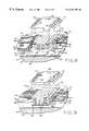
- FIG. 1is a partially exploded perspective view of an embodiment of the present invention.
- FIG. 2is a side elevational view in partial cross section of FIG. 1 .
- FIG. 3is an enlarged cross-sectional view of an indicated portion of FIG. 2 .
- FIG. 4is a top plan view of a copper foil interconnect pattern representative of the present invention.
- FIG. 5is a top plan view of a second copper foil interconnect pattern representative of the present invention.
- FIG. 6is a side elevational view in partial cross section of a second embodiment of the present invention.
- FIG. 7is an enlarged cross-sectional view of an indicated portion of FIG. 6 .
- FIG. 8is a partially exploded and enlarged perspective view of an indicated portion of FIG. 2 .
- FIG. 9is a partially exploded and enlarged perspective view of an indicated portion of FIG. 6 .
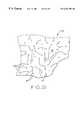
- FIG. 10is a top plan view of a portion of a generic wiring pattern.
- FIG. 11is a flow diagram illustrating a method for making the present invention.
- circuit elementspower transistors, capacitors, diodes, etc.
- circuit elementspower transistors, capacitors, diodes, etc.
- circuit elementsshown in the following various embodiments of the present invention are shown for illustrative purposes only. That is, the embodiments described herein are not functioning, working circuits. Instead, specific circuit components are shown merely to illustrate how the novel substrate of the present invention is capable of interconnecting various circuit elements and dissipating heat therefrom.
- the integrated substrate, or “module,” of the present inventionis shown generally at 20 and includes aluminum base 22 to which is bonded multilayer circuit board 24 .
- the substrateis capable of supporting many different circuit elements as shown in FIG. 1 .
- packaged componentssuch as transistors 26 , resistors 28 , and diode 30 can be surface mounted to top surface 32 of integrated substrate 20 .
- small capacitors 34 in chip formcan also be surface mounted to substrate 20 .
- Integrated circuit (IC) chipssuch as IC chip 36 as well as larger packaged components, such as transistor 37 , can also be surface mounted to substrate 20 .
- the substrate of the present inventionexhibits improved thermal characteristics so that “high power semiconductor” elements can be installed within substrate 20 .
- “Power semiconductor element,” “power element,” or “high power semiconductor element” in the context of this specificationis defined as a circuit element, either in packaged or die form having a power output greater than 10 amps and minimum of 10 Watts.
- Power semiconductorscan include, for example, power transistors and switches for high current devices.
- Power semiconductorscan also include MOSFETs, IGBTs, thyristors, triacs, SRCs, bipolar transistors, power amplifiers, GaAs devices, diodes, and voltage and current regulators.
- control circuit elementis defined herein as a circuit element having relatively low power output.
- Control semiconductor elementsinclude linear and digital circuits used to control the power elements and include common resistors, capacitors, IC chips, diodes and the like. Typical control circuitry would be drivers for power transistors, amplifiers, voltage and current regulators, D/A and A/D converters, logic functions and the like.
- both power and control elementscan be installed into a single integrated substrate 20 .
- the wiring, or “interconnect” patterns for both the power and control elementscan be included between top surface 32 and aluminum base 22 of substrate 20 , allowing a compact density of power and control elements.
- power semiconductor element 38is mounted in cavity 40 , which cavity is formed partially or fully into multilayer circuit board 24 .
- the bottom layer of substrate 20is comprised of a thick aluminum base 22 , which serves as a heatsink.
- heatsink base 22is substantially thicker than circuit board 24 .
- aluminum base 22can, advantageously, be of a shape that will serve as a structural member of the system in which the integrated substrate is used.
- base 22is a flat shape that can be punched, cut or machined from sheet material.
- aluminum base 22can be formed with fins (not shown) to enhance heat removal from substrate 20 .
- the type of aluminum material chosen for base 22is not significant in the present invention. There are virtually hundreds of different aluminum compositions commercially available. Furthermore, the material for base 22 could be made from a material other than aluminum, such as copper or other metals, and still remain within the scope of the present invention. In applications that require wire to be bound to aluminum base 22 , a material composition with less impurities would be required. Present designs have been made with aluminum type 6061, which has good mechanical strength, good thermal characteristics, and also exhibits good wire bonding characteristics.
- multilayer circuit board 24is shown bonded to aluminum base 22 .
- Multilayer circuit board 24can be comprised of varying numbers of layers and such layers can vary in arrangement, type and thickness, as explained below.
- FIGS. 1-3show one specific embodiment of multilayer circuit board 24 .
- Circuit board 24is bonded to aluminum base 22 with a thermally conductive organic bonding material shown at 44 .
- Bonding material 44should be electrically insulating and have excellent thermal characteristics.
- One suitable material for bonding material 44is Tgon-1KA, manufactured by Thermagon Inc.
- Tgon-1KAcombines a thermosetting epoxy with a boron nitride filler which forms a bonding material with excellent thermal characteristics, having a thermal conductivity of greater than 8 W/m-K.
- Tgon-1KAis fabricated in a B-stage form and is available in sheets that can be die-cut into the required shape and size.
- other thermally conductive materials available as a B-stage preparedcan be used as bonding material 44 in lieu of the Tgon-1KA, provided that such material exhibits excellent thermal characteristics, preferably greater than 8 W/m-K.
- the next layer above bonding material 44is “thick” copper foil interconnect pattern 46 .
- interconnect pattern 46is used to interconnect power element 38 to the control elements and also to the next stage in the assembly to which substrate 20 is connected.
- integrated substrate 20could be connected to a high torque motor, or similar device.
- the thickness of foil pattern 46is a function of required current carrying capacity of the particular module.
- the number and power output of power elements installed on a particular integrated substrate of the present inventionwill vary from one application to another. That is to say, multiple cavities (not shown) can be provided in top surface 32 with one or more power elements installed in each cavity. Accordingly, required current-carrying capabilities will vary.
- Typical thicknesses for foil 46range from 0.010 inches to 0.020 inches.
- Foil 46is formed into an interconnect pattern for substrate 20 , such as shown in FIGS. 4 and 5.
- Foil 46can also be formed with leads 48 as shown in FIGS. 4 and 5, which leads are used to connect the substrate to the next stage in the assembly (not shown).
- leads 48can be made to extend beyond the limits of the vertical walls of substrate 20 to aid in connection of substrate 20 with the next stage in the assembly.
- the thermal advantages of the thick foil pattern 46 installed in substrate 20become evident when considering the arrangement of power element 38 , foil 46 , bonding material 44 and base 22 .
- cavity 40is formed in multilayer circuit board 24 , which cavity exposes thick foil 46 .
- power element 38mounts directly to foil 46 .
- connecting wires 50electrically connect power element 50 to foil 46 .
- the superior heat conduction away from power element 38can be appreciated.
- element 38is mounted directly and fits flush against foil 46 .
- Foil 46which is formed typically from copper, serves as an excellent conductor of heat, so that heat generated by element 38 is conducted away by foil 46 .
- foil 46being the bottom layer of circuit board 24 , is bonded to aluminum heatsink 22 with thermally conductive bonding material 44 .
- thermally conductive bonding material 44exhibits excellent thermal properties so that heat is efficiently conducted away from foil 46 .
- heatsink 22having a high thermal conductivity, and because of its large size and thickness relative to power element 38 , absorbs the heat conducted through bonding material 44 .
- heatis efficiently transferred from power element 38 to heatsink 22 , allowing substrate 20 to integrate power and control elements without overheating.
- a thick copper foil, such as foil 46large amounts of heat are able to be dissipated without increasing the overall area occupied by the substrate.
- the thermally conductive and electrically insulating bonding materialpossesses such a high thermal conductivity that heat can be transferred efficiently to the aluminum heatsink, which heatsink also exhibits good thermal properties.
- the arrangement of layers shown in FIG. 3, in which power element interconnect 46 is positioned as the bottom layer of multilayer circuit board 24direct transfer of heat from interconnect 46 to heatsink 22 through bonding material 44 is achieved.
- the relative arrangement of components and layers of the substrate, as well as strategic positioning of thermal viasenhance the thermal properties of substrate 20 .
- circuit board 24is comprised of a series of layers, the sequence of which repeats, depending upon the ultimate number of layers required for the particular application.
- the layer immediately above and adjacent to thick foil 46is a standard prepared bonding material 52 , the composition of which is widely known in the art.
- Prepared material 52is used to bond thick foil 46 with thin foil interconnect pattern 54 as shown in FIG. 3 .
- conventional prepared material 52can be replaced with a highly thermally conductive and electrically insulating bonding material such as the Tgon-1KA used for layer 44 , as discussed above.
- Foil 54is the next adjacent layer in the substrate as shown in FIG. 3 .
- Foil 54is a typical thin copper foil used to interconnect control elements and its use is known to one of skill in the art. As used in the substrate of the present invention, foil 54 has a thickness typically in the range of 0.0005 to 0.002 inches. As shown in FIG. 3, layers 58 , 60 , 62 and 64 are also “thin” foils and have an appearance quite similar to layer 54 . A portion of a “generic” thin foil pattern 55 , shown in FIG. 10, is fairly representative of an interconnect pattern used in the multiple layers of the present invention to wire the control elements. These control interconnect patterns are interconnected using standard circuit board techniques. Interconnect wires 57 are arranged in a pattern corresponding with the particular circuit design and can electrically interconnect to other levels of the multilayer substrate through drilled and plated holes 59 as shown in FIG. 10 .
- the layer adjacent and above layer 54is a circuit board core material 66 .
- Core material 66can be selected from a variety of circuit board materials, such as polyimide-glass for example, and such core materials are widely known in the art.
- thin foil pattern 58Immediately above and adjacent to core material 66 is thin foil pattern 58 , and one can now appreciate that the sequence of materials in multilayer circuit board 24 has begun to repeat.
- adjacent and above foil pattern 58is prepared material 52 followed by interconnect pattern 60 , core material 66 , and interconnect 62 .
- the sequence of layers for multilayer circuit board 24repeats itself again with prepared material 52 , interconnect layer 64 , core material 66 , and finally top interconnect pattern 56 .
- control interconnect patternscan be connected to thick interconnect pattern 46 , which is used to interconnect power elements, such as element 38 .
- thermal characteristics of substrate 20can be enhanced by using “vias.”
- FIG. 8an enlarged and partially exploded portion of FIG. 2 is shown in detail. Certain parts, such as prepared material 52 and core material 66 , have been omitted from FIG. 8 for clarity. Furthermore, only portions of interconnect patterns 54 - 64 are shown in FIG. 8 so that the novel features of the present invention can be clearly illustrated.
- FIG. 8primarily illustrates the use of thermal vias in the present invention, which vias can be used to conduct heat and/or electric signals.
- a thermal viais a pipe, typically made from copper, which can be hollow or filled.
- vias 68are connected to thick copper interconnect 46 at their bottom end, and are connected to IC bonding pad 70 at their top end.
- IC chip 36shown as exploded away from pad 70 , is mounted to pad 70 in such a way so that the bottom surface of IC chip 36 is in contact and flush with pad 70 as shown in FIG. 2 .
- heatis conducted away from chip 36 through pad 70 , vias 68 , and into copper layer 46 .
- heatis ether dissipated to bonding material 44 and finally into aluminum heatsink 22 .
- viascan be used to conduct electricity from the thin interconnect patterns, such as top interconnect pattern 56 , to thick interconnect pattern 46 .
- vias 72connect to thick pattern 46 at their bottom end and connect to bond pads 74 at their top end. Electrical wires 73 from chip 36 connect to pads 74 when chip 36 is installed on substrate 20 . An electrical path is thereby created between chip 36 and thick interconnect pattern 46 .
- control circuitrysuch as chip 36 can be electrically connected to the thick interconnect pattern, which in turn interconnects power elements, such as element 38 .
- Viascan also be used to conduct electricity and heat from one layer of control interconnect to another.
- via 76connects from pad 74 on top interconnect layer 56 to another pad 77 on interconnect layer 54 , conducting electricity and heat therebetween.
- “Blind,” or “buried” viasare also possible.
- Buried via 80connects bonding pad 78 to bonding pad 79 , thereby providing an electrical and thermal connection between interconnect layer 64 and interconnect layer 62 .
- wires 57transmit electrical signals to other parts of the substrate.
- “Medium power elements,” such as a device with a power dissipation up to 5 Watts, and/or a current of less than 5 Acan be surface mounted to top surface 32 of substrate 20 .
- large packaged component 37may generate an amount of heat large enough so that surface mounting to top surface 32 would not be possible without heat dissipation benefits derived from the use of thermal vias.
- vias 81are installed into substrate 20 .
- IC chip 36 shown in FIGS. 1 and 8may need to operate at a relatively low temperature in order to avoid damage to the delicate components therein.
- thermal vias 70enhance heat removal and allow chip 36 to operate at a lower temperature.
- FIGS. 6, 7 and 9A second embodiment of the present invention is shown in FIGS. 6, 7 and 9 .
- Corresponding reference charactersindicate parts corresponding to the first embodiment.
- the second embodimentdiffers primarily from the first embodiment in the arrangement of layers in multilayer circuit board 24 .
- the bottom layer of substrate 20is base 22 , which serves as a heatsink.
- multilayer circuit board 24is bonded to heatsink 22 with a thermally conductive organic bonding material shown at 44 .
- the Tgon-1KA materialdiscussed above, is an exemplary material for bonding material 44 because of its excellent thermal properties.
- interconnect pattern 54is a typical thin copper foil used to interconnect control elements and its use is known to one of skill in the art.
- Foil 54has a thickness typically in the range of 0.0005 to 0.002 inches.
- layers 58 and 64are also “thin” foils and have an appearance quite similar to layer 54 .
- a portion of a “generic” thin foil pattern 55shown in FIG. 10, is fairly representative of an interconnect pattern used in all of the multiple layers of the present invention to wire the control elements. These control interconnect patterns are interconnected using standard circuit board techniques known in the art.
- interconnect wires 57are arranged in a pattern depending upon the particular circuit design and can electrically interconnect to other levels of the multilayer substrate through drilled and plated holes 59 .
- the bottom side of foil pattern 54is bonded to bonding material 44 whereas the top side of foil pattern 54 is connected to core material 66 , which is a standard circuit board core material.
- Core material 66can be selected from many circuit board core materials known in the art.
- Interconnect layer 58is connected to the top side of core material 66 .
- Layer 58is bonded to prepared bonding material 52 , which is comprised of a standard prepared bonding material widely known in the art.
- bonding material 52can be the same Tgon-1KA material used for bonding material 44 .
- Adjacent and bonded to the top side of prepared material 52is a layer of thick copper interconnect 46 .
- Layer 46interconnects the power elements, such as element 38 , in substrate 20 .
- Adjacent and on top of interconnect layer 46is core material 66 followed by another thick layer 46 , which also interconnects power elements.
- the second embodimentshows that more than one thick copper foil can be used to interconnect the power elements of substrate 20 . While, generally speaking, the most efficient heat dissipation is achieved from arranging interconnect pattern 46 as the bottom layer in circuit board 24 , several circuit board layers can be disposed between interconnect pattern 46 and base 22 .
- FIG. 7shows two thick interconnect patterns 46 sandwiched between two layers of prepared bonding material 52 , the interconnect patterns 46 being positioned several layers away from base 22 .
- the interconnect patterns 46being positioned several layers away from base 22 .
- a highly thermally conductive bonding materialsuch as the Tgon-1KA as bonding material 52 , especially adjacent power element interconnect layers, such as layers 46 .
- Separating the two thick copper layersis a core material 66 .
- the inventorshave found that the relative thickness of each layer can be decreased. For example, the present inventors have successfully built a substrate employing two layers 46 as shown in FIG. 7 with each layer 46 having an approximate thickness of 0.005 inches.
- layer 64is again a typical thin interconnect foil used in multilayer printed circuit boards and is used to interconnect control elements and has a general appearance as shown in FIG. 10 .
- Core material 66the second layer from the top of multilayer circuit board 24 , is comprised of the same core material as used for other layers 66 shown in FIG. 7 .
- top interconnect layer 56has a general appearance substantially the same as shown on top surface 32 in FIG. 1 .
- cavity 40 in multilayer circuit board 24differs from the cavity shown in the first embodiment because of the differing arrangement of thick copper layers in the first and second embodiments of the present invention.
- power element 38is bonded to heat spreader 86 .
- Heat spreader 86is typically comprised of copper although other suitable materials can be used for heat spreader 86 .
- Heat spreader 86is bonded to bonding material 44 , which in turn is bonded to aluminum heatsink 22 . Heat is thus transferred from power element 38 to heat spreader 86 and is further transferred to aluminum heatsink 22 through thermally conductive bonding material 44 .
- power element 38is electrically connected through wires 50 to bonding pads 89 .
- Via 91(shown in phantom lines) connects power element 38 into thick copper foils 46 .
- via 90connects IC chip 36 through wires 73 into the thick copper foils 46 .
- FIG. 9is a partially exploded enlarged perspective view of a portion of FIG. 6, the thermal and electrical connection between power elements, control elements, and interconnect patterns can be better understood.
- core material 66as well as prepare bonding material 52 are not shown in FIG. 9 .
- interconnect patterns 54 , 56 , 58 , and 64are shown in FIG. 9 so that the novel features of the present invention can be clearly illustrated.
- FIG. 9further illustrates the use of thermal vias in the present invention, which vias can be used to conduct heat and/or electric signals.
- vias 68are connected to a bonding pad 69 at their bottom ends and are connected to IC bonding pad 70 at their top ends. Bonding pads 69 and 70 can also be seen at the bottom and top of multilayer circuit board 24 in FIG. 6 .
- IC chip 36is shown as exploded away from pad 70 in FIG. 9 and is shown attached to pad 70 in FIG. 6 .
- chip 36When installed on substrate 20 , chip 36 is mounted to pad 70 , in such a way so that the bottom surface of IC chip 36 is in contact and flush with pad 70 as shown in FIG. 6 . Thus, heat is conducted away from chip 36 through pad 70 , vias 68 , and into bonding pad 69 , which acts as a heat spreader. Heat is in turn conducted to bonding material 44 and finally into aluminum heatsink 22 . Chip 36 can therefore be maintained at a lower temperature than without the presence of vias 68 .
- Viascan be used to connect control circuit elements into thick copper layers 46 . As shown in FIG. 9, via 72 electrically interconnects the two layers 46 of thick interconnect pattern. Further, via 72 electrically connects to bond pad 74 as shown. In turn, bond pad 74 electrically connects to wire 73 of IC Chip 36 . An electrical path is thereby created between chip 36 and thick interconnect patterns 46 . In this manner, control circuitry, such as chip 36 can be electrically connected to the thick interconnect pattern, which in turn interconnects power elements, such as element 38 .
- viascan be used to electrically and thermally connect two or more layers of control interconnect patterns. As shown in FIG. 9, via 94 connects from pad 75 on top interconnect layer 56 to another bonding pad 96 on interconnect layer 64 , conducting electricity and heat therebetween. Thus, a respective wire 73 conducts electricity from chip 36 to bond pad 75 , and electricity is further conducted to bond pad 96 through via 94 . Electrical signals are further transmitted to another part of the circuit through wires 57 .
- multilayer printed circuit board 24is fabricated using standard printed circuit board (“PCB”) manufacturing techniques into a structure that contains the interconnect for all low power circuitry associated with module 20 .
- PCBprinted circuit board
- layers 54 through 56 as shown in FIG. 2are fabricated as a first step.
- a double layer thick copper foil 46 as shown in FIGS. 6 and 7can be fabricated into circuit board 24 .
- all holes that are associated with the low power circuitryare drilled and plated.
- the last step of formation of circuit board 24is the lamination of thick copper foil pattern 46 .
- Foil 46can be etched into a pattern like that shown in FIGS. 4 and 5 prior to or after lamination. When the etching is done is dependent upon the foil thickness required for foil 46 . Thinner foils can be etched after lamination.
- Foil 46is laminated to the multi-layer circuit board using standard high temperature prepare material 52 and lamination processes well-known to one skilled in the art. If additional thermal paths are required for the lower power circuitry, the foil may be laminated using the Tgon-1KA material used to bond the foil 46 to aluminum base 22 .
- the cavities 40are either punched out or rounded out after lamination of the PCB structure, prior to lamination of the heatsink base, or prior to lamination of the thick copper foil and heat sink.
- Multilayer circuit board 24is then drilled and copper plated for all the power connections. Where medium power devices are to be surface mounted on top surface 32 as shown in FIG. 1, or enhanced thermal characteristics are needed, thermal vias are drilled and plated in an array capable of dissipating the appropriate power. Final overplating of nickel and optionally gold is then applied and the structure is ready for the final bonding process.
- thermally conductive organic bonding material 44such as Tgon-1KA, manufactured by Thermagon Inc.
- Tgon-1KAthermally conductive organic bonding material 44
- This materialcombines a thermosetting epoxy with a boron nitride filler to form a bonding material with excellent thermal characteristics.
- the thermal conductivity of material 44is greater than 8 Watts per meter per degree Kelvin.
- Material 44is fabricated in a B-stage form and is available in sheets that can be die-cut into the desired shape and size.
- Other thermally conductive material available as a B-stage preparecan be used in lieu of the Tgon-1KA, provided such bonding material also possesses the requisite thermal properties, such as thermal conductivity, coefficient of expansion, etc.
- thermal viasare installed, the vias would be connected to the thick copper layer 46 at the bottom of circuit board 24 as shown in FIG. 2, or alternatively, to thin copper layer 54 at the bottom of circuit board 24 as shown in FIG. 6 .
- heatis spread to thermally conductive bonding material 44 and aluminum base 22 .
- the bonding processstarts with an assembly of multilayer circuit board 24 , bonding material 44 and aluminum base 22 , which are stacked on top one another.
- This assemblyis put in a vacuum bag and evacuated to at least 25′′ Hg. for a minimum of 15 minutes.
- the evacuated assemblyis then placed in a laminating press capable of applying heat and pressure to the assembly.
- the assemblyis heated to a bonding temperature of 170° C.-175° C. and then a minimum pressure of 50 psi is applied to the assembly.
- the pressure requiredis a function of foil thickness and size.
- the bonding temperaturehas been reached, the vacuum is released.
- the assemblyis maintained at the cure temperature for a minimum of 1 hour, then cooled under pressure before being removed from the laminating press. If the substrates have been laminated in array form, the assembly can then be separated by routing.
- Each integrated substrateis then processed through an assembly process whereby power semiconductors are mounted in cavities, such as cavity 40 , and other devices are attached, either directly or on tabs.
- the appropriate sections of the assemblyare then overmolded using a compatible molding compound to protect the semiconductors from environmental effects.
Landscapes
- Engineering & Computer Science (AREA)
- Microelectronics & Electronic Packaging (AREA)
- Production Of Multi-Layered Print Wiring Board (AREA)
- Structure Of Printed Boards (AREA)
- Cooling Or The Like Of Semiconductors Or Solid State Devices (AREA)
Abstract
Description
1. Field of the Invention
The present invention generally relates to substrates which interconnect and dissipate heat from power semiconductor elements and more particularly to integrated substrates having enhanced thermal characteristics in which interconnecting wiring patterns for power and control circuit elements are combined.
2. Description of Related Art
Industry has been continually increasing the demand for higher speeds, smaller size, and increased power from circuit boards. Such design requirements are difficult to achieve with the concomitant requirement of removing the heat generated by high density high power designs.
The conventional approach to high density high power design has been the use of power hybrid microcircuits, which include an alumina ceramic substrate base onto which a current-carrying interconnect pattern is either deposited or screen printed. Unfortunately, this interconnect is not suitable for the high current generated by “power semiconductor elements.” Instead, “bonding islands” are solder mounted onto the interconnect and in turn, wires that are capable of carrying high current or power semiconductors are mounted onto the islands. The resulting assembly may require a hermetically packaged enclosure. Low current control circuitry, such as integrated circuits, transistors, resistors and capacitors, which serve as control circuits for the power semiconductors, are generally built on a separate substrate in the same enclosure or in a completely separate module.
One recent prior art approach to power modules involves chemically bonding a thin copper layer to an alumina (aluminum oxide) or aluminum nitride ceramic substrate using an oxide interface. The thin copper layer is then electroplated to increase its thickness to greater than 0.005 inches. The substrate is then used to interconnect high current devices. However, current carrying capability is a direct function of cross-sectional area and a high current device therefore requires either a wider or a thicker conductor to have sufficient cross-sectional area. The drawback with alumina or aluminum nitride ceramic substrates which use 0.005 inch thick copper is that these modules are not able to carry high currents without requiring a larger surface area on the module, thereby unsuitably increasing the overall size of the module.
Further developments in the area of alumina or aluminum nitride ceramic substrate technology include chemically bonding thicker copper foils, greater than 0.005 inches, to a ceramic substrate. Even with a thicker foil, however, ceramic based substrates have drawbacks. A ceramic based substrate generally must be mounted on a structural base, otherwise the brittle ceramic material can break. In most applications, size of the circuit is an important consideration, and it is undesirable to waste valuable space with the additional structural base required to support the ceramic substrate. Furthermore, even in applications where a structural base can be avoided, the brittle ceramic substrates require special fasteners to avoid breakage.
Using metal instead of a ceramic base is known in the art. For example, the design disclosed in U.S. Pat. No. 5,513,072 involves a common module containing a power semiconductor element, a circuit board for the power element, a circuit board for a control circuit and a heat spreader fixed on a metal plate. In this design, the power element is mounted onto the heat spreader, which is formed as a copper or copper clad island. In turn, the heat spreader is adhered to the metal plate by a high heat radiating insulating layer made of resin based material so that the heat spreader and the metal plate are electrically insulated from each other. The wiring pattern for the power semiconductor element is formed in a power circuit control board disposed adjacent to one side of the power element on the metal plate. Attached to the metal plate and placed on the opposite side of the power semiconductor is an additional circuit board which is used for wiring control circuitry.
A power module as disclosed by U.S. Pat. No. 5,513,072 includes high and low power devices on one base plate, but suffers drawbacks. First, the wiring pattern for the power semiconductor cannot be placed beneath the power semiconductor in such a design. Instead, a power circuit board is placed adjacent to the power element, thereby using more valuable space on the module. A design allowing the power element wiring pattern to be placed intermediate the power semiconductor element and the metal plate would save valuable space and achieve a smaller module. Furthermore, the design requires a separate heat spreader positioned between the power element and the metal base in order to dissipate heat. A thinner, cheaper module could be constructed if the heat spreader could be eliminated. Finally, a power module like that disclosed by U.S. Pat. No. 5,513,072 requires two separate circuit boards, one of which is for interconnecting high power elements while the other circuit board connects the low power circuitry. A power module having two instead of one circuit board adds a step to the manufacturing process, in turn increasing cost. Furthermore, a power module having two circuit boards requires a larger design than a power module with one circuit board.
It has been known to use thick copper foils in conjunction with metal substrates such as aluminum to remove heat generated by power semiconductors. One known device is an automotive power steering module that utilizes a large (8 inches by 4 inches) copper interconnect pattern bonded to an aluminum substrate. The interconnect pattern is approximately 0.020 inch thick and interconnects large power semiconductors and switches currents greater than 75 amperes. In such an application, the aluminum base serves not only as the mounting platform for the semiconductors but is also an integral part of the system, serving as a structural mounting member in the power steering assembly. In this known application, a low power interconnect using a single layer printed circuit board is bonded to the thick copper foil and provides control signal connections.
Another known product is a power module for a surgical saw. In this power module, a copper interconnect pattern having a thickness greater than 0.010 inches is again bonded to an aluminum substrate and is used to interconnect the switching power transistors that control the brushless motor in the surgical saw. The saw features a high torque which requires switching of currents greater than 30 amperes by the power module.
Yet another known prior art product is a power module for an automotive anti-lock braking system (“ABS system”). This known module also utilizes a thick copper interconnect pattern bonded to an aluminum substrate to interconnect power transistors and to switch the large currents required in the ABS system. As in the above described power steering module, the module for the automotive ABS system also is formed as an integral part of the system, thereby giving structural strength to the overall assembly.
Although some developments have been made in integrating power and control circuit elements while removing heat, it is desirable to further improve the interconnect density and the heat removal capacity of such substrates. It is thus desirable to have a single substrate that is able to (1) handle high currents generated by power semiconductors; (2) route many interconnections in a small area; (3) efficiently remove heat at a reduced cost; (4) integrate low power circuitry required to control high current devices; and (5) offer an overall reduction in size. In addition to these performance features, it is desirable to have an integrated substrate that lends itself to mass production at low cost.
The present invention overcomes the disadvantages of the above described prior art by providing a thermally efficient multi-layered integrated substrate having wiring patterns for both power semiconductor elements and control semiconductor elements disposed intermediate a top surface of the substrate and a heatsink base.
In one form, the present invention comprises an integrated substrate capable of interconnecting power and control circuit elements. The substrate comprises a base typically made from aluminum which acts as a heatsink. A multilayer printed circuit board is bonded to the base using a thermally conductive and electrically insulating bonding material. The thermally conductive and electrically insulating bonding material of the present invention has excellent thermal properties, namely a very high thermal conductivity. The circuit board includes a first foil interconnect pattern having a thickness greater than 0.010 inches. The first interconnect pattern is disposed intermediate the top surface of the circuit board and the bonding material. The circuit board also includes a second foil interconnect pattern having a thickness less than 0.002 inches. The second interconnect pattern is also disposed intermediate the top surface of the circuit board and the bonding material. A cavity is formed in the top surface of the circuit board and is adapted for receiving a power semiconductor element therein.
In another form, the present invention is an integrated module which comprises a thermally conductive base which acts as a heatsink. A multilayer printed circuit board having at least one control semiconductor element mounted thereto is bonded to the base using a thermally conductive and electrically insulating bonding material. A cavity is disposed in a top surface of the circuit board and a power semiconductor element is mounted in the cavity. The circuit board includes a first wiring pattern connected to the control semiconductor element and a second wiring pattern connected to the power semiconductor element. The first and second wiring patterns are electrically connected to each other.
In yet another form, the present invention comprises an integrated substrate adapted for integrating power and control semiconductor elements. The substrate comprises a thermally conductive base which serves as a heatsink. An electrically conductive foil interconnect pattern having a thickness greater than 0.010 inches is bonded to the base with a thermally conductive and electrically insulating bonding material. Thus, the bonding material is disposed between the base and the foil pattern and bonds the base to the foil pattern. The foil pattern forms a bottom layer of a multilayer circuit board and the circuit board has at least two layers of a control semiconductor element interconnect pattern. The base, bonding material, foil pattern, and the circuit board comprise a series of adjacent layers, respectively. A cavity disposed in a top surface of the circuit board and the foil pattern forms a bottom surface of the cavity.
In still another form, the present invention comprises a multi-layered substrate for supporting high power semiconductors and control elements. The substrate comprises a series of layers. The first layer comprises a base having thermally conductive properties and the base acts as a heatsink. A second layer is disposed adjacent the base and comprises an electrically insulating and thermally conductive bonding material. The bonding material is bonded to the base. A third layer is disposed adjacent the second layer and comprises either a thick copper foil interconnect or a thin copper foil interconnect pattern. The third layer is bonded to the second layer. A fourth layer is disposed adjacent the third layer and comprises a prepared material. The fourth layer is bonded to the third layer. A fifth layer is disposed adjacent the fourth layer and comprises either a thick copper foil interconnect or a thin copper foil interconnect pattern. The fifth layer is bonded to the fourth layer. A sixth layer is disposed adjacent the fifth layer and comprises a core circuit board material. The sixth layer is bonded to the fifth layer. At least one series of layers arranged substantially identically to the third through said sixth layers is bonded to the sixth layer. The series has a bottom layer corresponding to the third layer and a top layer corresponding to the sixth layer. The bottom layer of the series is adjacent to the sixth layer and bonded thereto. The thick copper foil has a thickness greater than 0.005 inches and the thin copper foil has a thickness less than 0.002 inches.
One advantage of the present invention is that it enables wiring patterns for both high power semiconductor elements and control elements to be layered on top of each other in a single module, instead of side-by-side. Yet the present invention, because of its enhanced thermal properties, is still able to dissipate the heat generated by the high power elements without allowing the substrate to overheat. Thus, the present invention allows an integrated substrate to be built more compactly than, for example, a substrate having separate circuit boards for control and power elements with such separate circuit boards being placed side by side. Similarly, the present invention allows an integrated substrate to be built more compactly than a substrate having wiring patterns positioned side-by-side.
Another advantage, related to the first advantage, is that the enhanced thermal properties of the present invention allow a layer upon layer arrangement of power and control wiring patterns spaced relatively closely together. Thus, in addition to decreasing the width and depth of an integrated substrate, the present invention allows a reduction in relative height as well. Furthermore, such a multilayer structure of the present invention allows the mounting and interconnecting of low power devices, such as integrated circuits, transistors, diodes, resistors and capacitors in close proximity to the high power devices.
Another advantage of the present invention is its flexibility. In applications where heat dissipation from the power wiring pattern is at its highest, the wiring pattern for the power elements can be arranged closest to the aluminum heatsink, thereby creating a direct and thus efficient path for thermal transfer. On the other hand, in applications where less heat is generated, the interconnect wiring patterns for the power elements can be arranged in different locations within the multi-layered circuit board, thereby saving manufacturing costs.
Yet another advantage of the present invention is that by using thermal vias, the thermal properties of an integrated substrate of the present invention can be further enhanced. For example, heat produced by a medium power semiconductor element surface mounted to the top surface of an integrated substrate of the present invention can be dissipated by placing thermal vias beneath the bottom surface of the medium power element. The thermal vias extend through the substrate and thereby dissipate heat into the aluminum heatsink.
Another advantage of the present invention is that the aluminum base material has a high thermal conductivity. Thus, heat generated by high power semiconductors can be efficiently dissipated.
Yet another advantage of the present invention is that the aluminum base can be machined, pressed, punched, drawn etc. into shapes that can form an integral part of the overall system which uses the power module. Unlike fragile prior art ceramic material, the aluminum base of the present invention can be shaped and formed as a structural member, giving structural stability to the overall assembly in which it is employed.
Yet another advantage of the present invention relates to cost savings during manufacturing. The multilayer printed circuit board structure, including the thick copper foil, can be manufactured using standard printed circuit board manufacturing techniques commonly available throughout the industry. Further, the manufacturing of the structure can be done in a multiple-up configuration, i.e., manufacturing is done in an array of devices which lowers the manufacturing cost. Furthermore, the integrated structure of the present invention allows for mounting an interconnection of elements using surface mount technology and/or bare die technology, thereby giving the manufacturer the choice of the lowest cost assembly technology available.
Yet another advantage of the present invention is that the thermally conductive material used to bond the multilayer circuit board to the aluminum exhibits excellent thermal properties, such as a high thermal conductivity. Thus, the bonding material is an excellent conductor of heat between the multilayer circuit board and the base, yet the bonding material still electrically isolates the copper foil interconnect pattern from the aluminum base.
Still another advantage of the present invention is that the thermally conductive and electrically insulating bonding material exhibits sufficient bonding characteristics so that an effective and durable bond is formed between the multilayer circuit board and the aluminum base heatsink, and at the same time, heat dissipates efficiently through the bonding material.
Still another advantage of the present invention is that power semiconductors can be interconnected on the substrate without separate leads. Instead, they are interconnected using thick copper foil patterns. Additionally, the leads that interconnect a power module to its next assembly can be fabricated as an integral part of the copper foil pattern, thereby obviating the need to attach separate leads.
Still another advantage of the present invention is that it solves the high current problem by using a thick copper foil pattern having low electrical resistance so that unwanted heating effects are eliminated. Yet, even with a thick copper foil pattern, the present invention still maintains excellent thermal conductivity away from the copper foil through the use of the highly thermally conductive bonding material and the aluminum base.
The above-mentioned and other features and advantages of this invention, and the manner of attaining them, will become more apparent and the invention will be better understood by reference to the following description of an embodiment of the invention taken in conjunction with the accompanying drawings, wherein:
FIG. 1 is a partially exploded perspective view of an embodiment of the present invention.
FIG. 2 is a side elevational view in partial cross section of FIG.1.
FIG. 3 is an enlarged cross-sectional view of an indicated portion of FIG.2.
FIG. 4 is a top plan view of a copper foil interconnect pattern representative of the present invention.
FIG. 5 is a top plan view of a second copper foil interconnect pattern representative of the present invention.
FIG. 6 is a side elevational view in partial cross section of a second embodiment of the present invention.
FIG. 7 is an enlarged cross-sectional view of an indicated portion of FIG.6.
FIG. 8 is a partially exploded and enlarged perspective view of an indicated portion of FIG.2.
FIG. 9 is a partially exploded and enlarged perspective view of an indicated portion of FIG.6.
FIG. 10 is a top plan view of a portion of a generic wiring pattern.
FIG. 11 is a flow diagram illustrating a method for making the present invention.
Corresponding reference characters indicate corresponding parts throughout the several views. Although the drawings represent embodiments of the present invention, the drawings are not necessarily to scale and certain features may be exaggerated while other features may be omitted in order to better illustrate and explain the present invention. The exemplification set out herein illustrates embodiments of the present invention, in different forms, and such forms are not to be construed as limiting the scope of the invention in any manner.
It is to be understood that specific circuit elements (power transistors, capacitors, diodes, etc.) shown in the following various embodiments of the present invention are shown for illustrative purposes only. That is, the embodiments described herein are not functioning, working circuits. Instead, specific circuit components are shown merely to illustrate how the novel substrate of the present invention is capable of interconnecting various circuit elements and dissipating heat therefrom.
An exemplary embodiment of the substrate of the present invention is shown in the drawings, in particular by referring to FIG.1. The integrated substrate, or “module,” of the present invention is shown generally at20 and includesaluminum base 22 to which is bondedmultilayer circuit board 24. The substrate is capable of supporting many different circuit elements as shown in FIG.1. For example, packaged components such astransistors 26,resistors 28, anddiode 30 can be surface mounted totop surface 32 ofintegrated substrate 20. In addition to package components,small capacitors 34 in chip form can also be surface mounted tosubstrate 20. Integrated circuit (IC) chips such asIC chip 36 as well as larger packaged components, such astransistor 37, can also be surface mounted tosubstrate 20.
Significantly, the substrate of the present invention exhibits improved thermal characteristics so that “high power semiconductor” elements can be installed withinsubstrate 20. “Power semiconductor element,” “power element,” or “high power semiconductor element” in the context of this specification is defined as a circuit element, either in packaged or die form having a power output greater than 10 amps and minimum of 10 Watts. Power semiconductors, can include, for example, power transistors and switches for high current devices. Power semiconductors can also include MOSFETs, IGBTs, thyristors, triacs, SRCs, bipolar transistors, power amplifiers, GaAs devices, diodes, and voltage and current regulators. Further, a “control circuit element,” “control element,” or “control semiconductor element” is defined herein as a circuit element having relatively low power output. Control semiconductor elements include linear and digital circuits used to control the power elements and include common resistors, capacitors, IC chips, diodes and the like. Typical control circuitry would be drivers for power transistors, amplifiers, voltage and current regulators, D/A and A/D converters, logic functions and the like.
Having defined “power” and “control” elements, a feature of the present invention is that both power and control elements can be installed into a singleintegrated substrate 20. Further, the wiring, or “interconnect” patterns for both the power and control elements can be included betweentop surface 32 andaluminum base 22 ofsubstrate 20, allowing a compact density of power and control elements. With reference to FIG. 1,power semiconductor element 38 is mounted incavity 40, which cavity is formed partially or fully intomultilayer circuit board 24.
The advantages of the integrated substrate of the present invention will become clear from considering the novel arrangement of materials in a specific embodiment. First, with reference to FIGS. 1 through 3, the bottom layer ofsubstrate 20 is comprised of athick aluminum base 22, which serves as a heatsink. As shown in FIG. 1,heatsink base 22 is substantially thicker thancircuit board 24. Although shown as a rectangular shape in FIG. 1,aluminum base 22 can, advantageously, be of a shape that will serve as a structural member of the system in which the integrated substrate is used. Generally,base 22 is a flat shape that can be punched, cut or machined from sheet material. However,aluminum base 22 can be formed with fins (not shown) to enhance heat removal fromsubstrate 20.
The type of aluminum material chosen forbase 22 is not significant in the present invention. There are virtually hundreds of different aluminum compositions commercially available. Furthermore, the material forbase 22 could be made from a material other than aluminum, such as copper or other metals, and still remain within the scope of the present invention. In applications that require wire to be bound toaluminum base 22, a material composition with less impurities would be required. Present designs have been made with aluminum type 6061, which has good mechanical strength, good thermal characteristics, and also exhibits good wire bonding characteristics.
Turning again to FIGS. 1-3, and particularly to FIG. 3, which shows an enlarged view of the layers ofsubstrate 20,multilayer circuit board 24 is shown bonded toaluminum base 22.Multilayer circuit board 24 can be comprised of varying numbers of layers and such layers can vary in arrangement, type and thickness, as explained below. FIGS. 1-3 show one specific embodiment ofmultilayer circuit board 24.Circuit board 24 is bonded toaluminum base 22 with a thermally conductive organic bonding material shown at44.Bonding material 44 should be electrically insulating and have excellent thermal characteristics. One suitable material forbonding material 44 is Tgon-1KA, manufactured by Thermagon Inc. Tgon-1KA combines a thermosetting epoxy with a boron nitride filler which forms a bonding material with excellent thermal characteristics, having a thermal conductivity of greater than 8 W/m-K. Tgon-1KA is fabricated in a B-stage form and is available in sheets that can be die-cut into the required shape and size. However, other thermally conductive materials available as a B-stage prepared can be used as bondingmaterial 44 in lieu of the Tgon-1KA, provided that such material exhibits excellent thermal characteristics, preferably greater than 8 W/m-K.
The next layer abovebonding material 44, as seen in FIG. 3, is “thick” copperfoil interconnect pattern 46. In the embodiment shown in FIGS. 1 through 3,interconnect pattern 46 is used to interconnectpower element 38 to the control elements and also to the next stage in the assembly to whichsubstrate 20 is connected. For example, integratedsubstrate 20 could be connected to a high torque motor, or similar device. The thickness offoil pattern 46 is a function of required current carrying capacity of the particular module. The number and power output of power elements installed on a particular integrated substrate of the present invention will vary from one application to another. That is to say, multiple cavities (not shown) can be provided intop surface 32 with one or more power elements installed in each cavity. Accordingly, required current-carrying capabilities will vary. Typical thicknesses forfoil 46 range from 0.010 inches to 0.020 inches.Foil 46 is formed into an interconnect pattern forsubstrate 20, such as shown in FIGS. 4 and 5.Foil 46 can also be formed withleads 48 as shown in FIGS. 4 and 5, which leads are used to connect the substrate to the next stage in the assembly (not shown). Although it is not shown in the drawings, leads48 can be made to extend beyond the limits of the vertical walls ofsubstrate 20 to aid in connection ofsubstrate 20 with the next stage in the assembly.
The thermal advantages of thethick foil pattern 46 installed insubstrate 20 become evident when considering the arrangement ofpower element 38,foil 46,bonding material 44 andbase 22. With reference to FIGS. 1 and 2,cavity 40 is formed inmultilayer circuit board 24, which cavity exposesthick foil 46. With reference to FIG. 1,power element 38 mounts directly to foil46. As shown in FIG. 2, connectingwires 50 electrically connectpower element 50 to foil46. With reference to FIG. 2, the superior heat conduction away frompower element 38 can be appreciated. First,element 38 is mounted directly and fits flush againstfoil 46.Foil 46, which is formed typically from copper, serves as an excellent conductor of heat, so that heat generated byelement 38 is conducted away byfoil 46. Next,foil 46, being the bottom layer ofcircuit board 24, is bonded toaluminum heatsink 22 with thermallyconductive bonding material 44. As explained above, thermallyconductive bonding material 44 exhibits excellent thermal properties so that heat is efficiently conducted away fromfoil 46. Finally,heatsink 22, having a high thermal conductivity, and because of its large size and thickness relative topower element 38, absorbs the heat conducted throughbonding material 44.
Thus, heat is efficiently transferred frompower element 38 toheatsink 22, allowingsubstrate 20 to integrate power and control elements without overheating. Several factors make this novel design possible. First, by using a thick copper foil, such asfoil 46, large amounts of heat are able to be dissipated without increasing the overall area occupied by the substrate. Second, as mentioned, the thermally conductive and electrically insulating bonding material possesses such a high thermal conductivity that heat can be transferred efficiently to the aluminum heatsink, which heatsink also exhibits good thermal properties. Further, in the arrangement of layers shown in FIG. 3, in whichpower element interconnect 46 is positioned as the bottom layer ofmultilayer circuit board 24, direct transfer of heat frominterconnect 46 to heatsink22 throughbonding material 44 is achieved. Thus, the relative arrangement of components and layers of the substrate, as well as strategic positioning of thermal vias, as will be explained below, enhance the thermal properties ofsubstrate 20.
In a substrate of the present invention,circuit board 24 is comprised of a series of layers, the sequence of which repeats, depending upon the ultimate number of layers required for the particular application. With reference to FIG. 3, the layer immediately above and adjacent tothick foil 46 is a standardprepared bonding material 52, the composition of which is widely known in the art.Prepared material 52 is used to bondthick foil 46 with thinfoil interconnect pattern 54 as shown in FIG.3. For particularly high heat applications, conventionalprepared material 52 can be replaced with a highly thermally conductive and electrically insulating bonding material such as the Tgon-1KA used forlayer 44, as discussed above.
Returning now to the arrangement of layers ofcircuit board 24 shown in FIG. 3, the layer adjacent and abovelayer 54 is a circuitboard core material 66.Core material 66 can be selected from a variety of circuit board materials, such as polyimide-glass for example, and such core materials are widely known in the art. Immediately above and adjacent tocore material 66 isthin foil pattern 58, and one can now appreciate that the sequence of materials inmultilayer circuit board 24 has begun to repeat. Thus, adjacent and abovefoil pattern 58 isprepared material 52 followed byinterconnect pattern 60,core material 66, andinterconnect 62. The sequence of layers formultilayer circuit board 24 repeats itself again withprepared material 52,interconnect layer 64,core material 66, and finallytop interconnect pattern 56.
As suggested above, the control interconnect patterns can be connected tothick interconnect pattern 46, which is used to interconnect power elements, such aselement 38. Additionally, the thermal characteristics ofsubstrate 20 can be enhanced by using “vias.” Turning now to FIG. 8, an enlarged and partially exploded portion of FIG. 2 is shown in detail. Certain parts, such asprepared material 52 andcore material 66, have been omitted from FIG. 8 for clarity. Furthermore, only portions of interconnect patterns54-64 are shown in FIG. 8 so that the novel features of the present invention can be clearly illustrated.
At the bottom of FIG. 8 is shownaluminum heatsink 22, to which thermallyconductive bonding material 44 is bonded.Thick copper foil 46 is bonded tobonding material 44. FIG. 8 primarily illustrates the use of thermal vias in the present invention, which vias can be used to conduct heat and/or electric signals. A thermal via is a pipe, typically made from copper, which can be hollow or filled. For example, as seen in FIG. 8, vias68 are connected tothick copper interconnect 46 at their bottom end, and are connected toIC bonding pad 70 at their top end.IC chip 36, shown as exploded away frompad 70, is mounted to pad70 in such a way so that the bottom surface ofIC chip 36 is in contact and flush withpad 70 as shown in FIG.2. Thus, with reference to FIG. 8, heat is conducted away fromchip 36 throughpad 70, vias68, and intocopper layer 46. In turn, heat is ether dissipated tobonding material 44 and finally intoaluminum heatsink 22.
In addition to enhancing heat removal, vias can be used to conduct electricity from the thin interconnect patterns, such astop interconnect pattern 56, tothick interconnect pattern 46. As shown in FIG. 8, vias72 connect tothick pattern 46 at their bottom end and connect to bondpads 74 at their top end.Electrical wires 73 fromchip 36 connect topads 74 whenchip 36 is installed onsubstrate 20. An electrical path is thereby created betweenchip 36 andthick interconnect pattern 46. In this manner, control circuitry, such aschip 36 can be electrically connected to the thick interconnect pattern, which in turn interconnects power elements, such aselement 38.
Vias can also be used to conduct electricity and heat from one layer of control interconnect to another. For example, via76 connects frompad 74 ontop interconnect layer 56 to anotherpad 77 oninterconnect layer 54, conducting electricity and heat therebetween. “Blind,” or “buried” vias are also possible. Buried via80, for example, connectsbonding pad 78 tobonding pad 79, thereby providing an electrical and thermal connection betweeninterconnect layer 64 andinterconnect layer 62. In turn,wires 57 transmit electrical signals to other parts of the substrate.
By employing the use of vias as described above, circuit implementation can be optimized. “Medium power elements,” such as a device with a power dissipation up to 5 Watts, and/or a current of less than 5 A can be surface mounted totop surface 32 ofsubstrate 20. For example, with reference to FIG. 1, large packagedcomponent 37 may generate an amount of heat large enough so that surface mounting totop surface 32 would not be possible without heat dissipation benefits derived from the use of thermal vias. Thus, as seen in FIG. 1, vias81 are installed intosubstrate 20. Similarly,IC chip 36 shown in FIGS. 1 and 8 may need to operate at a relatively low temperature in order to avoid damage to the delicate components therein. With reference to FIG. 1,thermal vias 70 enhance heat removal and allowchip 36 to operate at a lower temperature.
A second embodiment of the present invention is shown in FIGS. 6,7 and9. Corresponding reference characters indicate parts corresponding to the first embodiment. The second embodiment differs primarily from the first embodiment in the arrangement of layers inmultilayer circuit board 24.
Turning now to FIGS. 6 and 7, the bottom layer ofsubstrate 20 isbase 22, which serves as a heatsink. With reference to FIG. 7,multilayer circuit board 24 is bonded to heatsink22 with a thermally conductive organic bonding material shown at44. The Tgon-1KA material, discussed above, is an exemplary material forbonding material 44 because of its excellent thermal properties.
The next layer above andadjacent bonding material 44 as seen in FIG. 7 isinterconnect pattern 54. As in the first embodiment, described above,foil 54 is a typical thin copper foil used to interconnect control elements and its use is known to one of skill in the art.Foil 54 has a thickness typically in the range of 0.0005 to 0.002 inches. As shown in FIG. 7, layers58 and64 are also “thin” foils and have an appearance quite similar tolayer 54. A portion of a “generic”thin foil pattern 55, shown in FIG. 10, is fairly representative of an interconnect pattern used in all of the multiple layers of the present invention to wire the control elements. These control interconnect patterns are interconnected using standard circuit board techniques known in the art. As shown in FIG. 10,interconnect wires 57 are arranged in a pattern depending upon the particular circuit design and can electrically interconnect to other levels of the multilayer substrate through drilled and plated holes59.
The bottom side offoil pattern 54 is bonded tobonding material 44 whereas the top side offoil pattern 54 is connected tocore material 66, which is a standard circuit board core material.Core material 66 can be selected from many circuit board core materials known in the art.Interconnect layer 58 is connected to the top side ofcore material 66.Layer 58 is bonded toprepared bonding material 52, which is comprised of a standard prepared bonding material widely known in the art. Alternatively,bonding material 52 can be the same Tgon-1KA material used for bondingmaterial 44.
Adjacent and bonded to the top side ofprepared material 52 is a layer ofthick copper interconnect 46.Layer 46 interconnects the power elements, such aselement 38, insubstrate 20. Adjacent and on top ofinterconnect layer 46 iscore material 66 followed by anotherthick layer 46, which also interconnects power elements. Thus, unlike the first described embodiment, wherein only one layer of thick interconnect foil was employed, the second embodiment shows that more than one thick copper foil can be used to interconnect the power elements ofsubstrate 20. While, generally speaking, the most efficient heat dissipation is achieved from arranginginterconnect pattern 46 as the bottom layer incircuit board 24, several circuit board layers can be disposed betweeninterconnect pattern 46 andbase 22. Thus, FIG. 7 shows twothick interconnect patterns 46 sandwiched between two layers ofprepared bonding material 52, theinterconnect patterns 46 being positioned several layers away frombase 22. Depending upon the heat generated bycopper layers 46, it may be desirable to use a highly thermally conductive bonding material such as the Tgon-1KA as bondingmaterial 52, especially adjacent power element interconnect layers, such as layers46. However, it has been found that adequate heat dissipation can usually be achieved by using a standard prepare bonding material. Separating the two thick copper layers is acore material 66. When two or more interconnect layers are employed to interconnect power elements, the inventors have found that the relative thickness of each layer can be decreased. For example, the present inventors have successfully built a substrate employing twolayers 46 as shown in FIG. 7 with eachlayer 46 having an approximate thickness of 0.005 inches.
As further shown in FIG. 7, three remaining layers abovelayer 52 completemultilayer circuit board 24.Layer 64 is again a typical thin interconnect foil used in multilayer printed circuit boards and is used to interconnect control elements and has a general appearance as shown in FIG.10.Core material 66, the second layer from the top ofmultilayer circuit board 24, is comprised of the same core material as used forother layers 66 shown in FIG.7. Finally,top interconnect layer 56 has a general appearance substantially the same as shown ontop surface 32 in FIG.1.
As shown in FIG. 6,cavity 40 inmultilayer circuit board 24 differs from the cavity shown in the first embodiment because of the differing arrangement of thick copper layers in the first and second embodiments of the present invention. With reference to FIG. 6,power element 38 is bonded to heatspreader 86.Heat spreader 86 is typically comprised of copper although other suitable materials can be used forheat spreader 86.Heat spreader 86 is bonded tobonding material 44, which in turn is bonded toaluminum heatsink 22. Heat is thus transferred frompower element 38 to heatspreader 86 and is further transferred toaluminum heatsink 22 through thermallyconductive bonding material 44. As shown in FIG. 6,power element 38 is electrically connected throughwires 50 tobonding pads 89. Via91 (shown in phantom lines) connectspower element 38 into thick copper foils46. Similarly, as shown in FIG.6 and explained in further detail below, via90 connectsIC chip 36 throughwires 73 into the thick copper foils46.
Turning now to FIG. 9, which is a partially exploded enlarged perspective view of a portion of FIG. 6, the thermal and electrical connection between power elements, control elements, and interconnect patterns can be better understood. For clarity of illustration,core material 66 as well as preparebonding material 52 are not shown in FIG.9. Furthermore, only portions ofinterconnect patterns
At the bottom of FIG. 9 is shownaluminum heatsink 22, to which thermallyconductive bonding material 44 is bonded. FIG. 9 further illustrates the use of thermal vias in the present invention, which vias can be used to conduct heat and/or electric signals. For example, vias68 are connected to abonding pad 69 at their bottom ends and are connected toIC bonding pad 70 at their top ends.Bonding pads multilayer circuit board 24 in FIG.6.IC chip 36 is shown as exploded away frompad 70 in FIG.9 and is shown attached to pad70 in FIG.6. When installed onsubstrate 20,chip 36 is mounted to pad70, in such a way so that the bottom surface ofIC chip 36 is in contact and flush withpad 70 as shown in FIG.6. Thus, heat is conducted away fromchip 36 throughpad 70, vias68, and intobonding pad 69, which acts as a heat spreader. Heat is in turn conducted tobonding material 44 and finally intoaluminum heatsink 22.Chip 36 can therefore be maintained at a lower temperature than without the presence ofvias 68.
Vias can be used to connect control circuit elements into thick copper layers46. As shown in FIG. 9, via72 electrically interconnects the twolayers 46 of thick interconnect pattern. Further, via72 electrically connects to bondpad 74 as shown. In turn,bond pad 74 electrically connects to wire73 ofIC Chip 36. An electrical path is thereby created betweenchip 36 andthick interconnect patterns 46. In this manner, control circuitry, such aschip 36 can be electrically connected to the thick interconnect pattern, which in turn interconnects power elements, such aselement 38.
Additionally, vias can be used to electrically and thermally connect two or more layers of control interconnect patterns. As shown in FIG. 9, via94 connects frompad 75 ontop interconnect layer 56 to anotherbonding pad 96 oninterconnect layer 64, conducting electricity and heat therebetween. Thus, arespective wire 73 conducts electricity fromchip 36 tobond pad 75, and electricity is further conducted tobond pad 96 through via94. Electrical signals are further transmitted to another part of the circuit throughwires 57.
With reference to FIG. 11, the preferred method of manufacturing the present invention is now explained.
First, several layers of multilayer printedcircuit board 24, shown in FIGS. 1 and 2, are fabricated using standard printed circuit board (“PCB”) manufacturing techniques into a structure that contains the interconnect for all low power circuitry associated withmodule 20. In other words, layers54 through56 as shown in FIG. 2 are fabricated as a first step. As noted, in some applications, a double layerthick copper foil 46 as shown in FIGS. 6 and 7 can be fabricated intocircuit board 24. During the fabrication process, all holes that are associated with the low power circuitry are drilled and plated.
In embodiments such as the first embodiment described above and shown in FIGS. 1-3 and8, where a single thick copperfoil interconnect pattern 46 is employed, the last step of formation ofcircuit board 24 is the lamination of thickcopper foil pattern 46.Foil 46 can be etched into a pattern like that shown in FIGS. 4 and 5 prior to or after lamination. When the etching is done is dependent upon the foil thickness required forfoil 46. Thinner foils can be etched after lamination.Foil 46 is laminated to the multi-layer circuit board using standard high temperature preparematerial 52 and lamination processes well-known to one skilled in the art. If additional thermal paths are required for the lower power circuitry, the foil may be laminated using the Tgon-1KA material used to bond thefoil 46 toaluminum base 22.
Thecavities 40 are either punched out or rounded out after lamination of the PCB structure, prior to lamination of the heatsink base, or prior to lamination of the thick copper foil and heat sink.
Next,multilayer circuit board 24 andaluminum base 22 are bonded together with thermally conductiveorganic bonding material 44, such as Tgon-1KA, manufactured by Thermagon Inc. This material combines a thermosetting epoxy with a boron nitride filler to form a bonding material with excellent thermal characteristics. The thermal conductivity ofmaterial 44 is greater than 8 Watts per meter per degree Kelvin.Material 44 is fabricated in a B-stage form and is available in sheets that can be die-cut into the desired shape and size. Other thermally conductive material available as a B-stage prepare can be used in lieu of the Tgon-1KA, provided such bonding material also possesses the requisite thermal properties, such as thermal conductivity, coefficient of expansion, etc.
Where thermal vias are installed, the vias would be connected to thethick copper layer 46 at the bottom ofcircuit board 24 as shown in FIG. 2, or alternatively, tothin copper layer 54 at the bottom ofcircuit board 24 as shown in FIG.6. Thus, in use ofsubstrate 20, heat is spread to thermallyconductive bonding material 44 andaluminum base 22.
The bonding process starts with an assembly ofmultilayer circuit board 24,bonding material 44 andaluminum base 22, which are stacked on top one another. This assembly is put in a vacuum bag and evacuated to at least 25″ Hg. for a minimum of 15 minutes. The evacuated assembly is then placed in a laminating press capable of applying heat and pressure to the assembly. The assembly is heated to a bonding temperature of 170° C.-175° C. and then a minimum pressure of 50 psi is applied to the assembly. The pressure required is a function of foil thickness and size. When the bonding temperature has been reached, the vacuum is released. The assembly is maintained at the cure temperature for a minimum of 1 hour, then cooled under pressure before being removed from the laminating press. If the substrates have been laminated in array form, the assembly can then be separated by routing.
Each integrated substrate is then processed through an assembly process whereby power semiconductors are mounted in cavities, such ascavity 40, and other devices are attached, either directly or on tabs. The appropriate sections of the assembly are then overmolded using a compatible molding compound to protect the semiconductors from environmental effects.
While this invention has been described as having a preferred design, the present invention can be further modified within the spirit and scope of this disclosure. This application is therefore intended to cover any variations, uses, or adaptations of the invention using its general principles. Further, this application is intended to cover such departures from the present disclosure as come within known or customary practice in the art to which this invention pertains and which fall within the limits of the appended claims.
Claims (53)
1. An integrated substrate capable of interconnecting power and control circuit elements, said substrate comprising:
a heatsink base having thermal conductive properties;
a multilayer printed circuit board;
a thermally conductive and electrically insulating bonding material which bonds said circuit board to said base;
said circuit board including a first foil interconnect pattern having a thickness greater than 0.005 inches, said first interconnect pattern disposed intermediate a top surface of said circuit board and said bonding material;
said circuit board including a second foil interconnect pattern having a thickness less than 0.002 inches, said second interconnect pattern disposed intermediate said top surface of said circuit board and said bonding material; and
a cavity disposed on said top surface of said circuit board adapted for installing a power semiconductor element therein, said first foil interconnect pattern being accessible through said cavity.
2. The substrate of claim1, wherein a power semiconductor element is mounted in said cavity and electrically connected to said first foil pattern.
3. The substrate of claim2, wherein a control circuit element is connected to said circuit board, whereby said control circuit element controls said power semiconductor element.
4. The substrate of claim3, wherein said control circuit element is electrically connected to said second foil pattern.
5. The substrate of claim3, wherein said power semiconductor element has a power output of greater than 5 Watts.
6. The substrate of claim1, wherein said cavity comprises a plurality of cavities and a plurality of control circuit elements are connected to said substrate.
7. The substrate of claim6, wherein each said cavity has installed therein at least one power semiconductor element, the power semiconductor elements are controlled by the control circuit elements, and the power semiconductor elements in the aggregate generate a total power output of greater than 5 Watts.
8. The substrate of claim1, wherein said first interconnect is electrically connected to said second interconnect.
9. The substrate of claim1, wherein said base is made of aluminum and wherein said first and second foil patterns are made of copper.
10. The substrate of claim1, wherein a thermal via is disposed in said circuit board, said thermal via thermally connects said first foil interconnect pattern to said base.
11. The substrate of claim1, wherein a thermal via is disposed in said circuit board, said thermal via electrically connects said first foil interconnect pattern to said second interconnect pattern.
12. The substrate of claim1, wherein:
a thermal via is disposed in said circuit board;
a first end of said thermal via is contiguous with said top surface of said circuit board and a second end of said thermal via is contiguous with a bottom surface of said circuit board and in thermal contact with said base.
13. The substrate of claim1, wherein:
a thermal via is disposed in said circuit board;
said via has a top and bottom end;
said top and bottom ends are disposed intermediate said top surface and said bonding material.
14. The substrate of claim1, wherein said first interconnect pattern comprises a plurality of layers, said layers thermally and electrically connected by at least one thermal via.
15. The substrate of claim1, wherein said bonding material combines a thermosetting epoxy with a boron nitride filler.
16. The substrate of claim1, wherein said bonding material has a thermal conductivity of at least 8 Watts per meter per degree kelvin.
17. The substrate of claim1, wherein said second interconnect pattern comprises a plurality of interconnect patterns.
18. The substrate of claim1, wherein said first interconnect pattern comprises a plurality of interconnect patterns.
19. The substrate of claim1, wherein said base is significantly thicker than said multilayer circuit board.
20. An integrated substrate having enhanced thermal properties comprising:
a thermally conductive heatsink base;
a multilayer printed circuit board having at least one control semiconductor element mounted to a top surface thereof;
a thermally conductive and electrically insulating bonding material which bonds said circuit board to said base;
a cavity disposed in a top surface of said circuit board, a power semiconductor element mounted in said cavity;
said circuit board including a first wiring pattern connected to the control semiconductor element;
said circuit board including a second wiring pattern connected to the power semiconductor element; and
said first wiring pattern electrically connected to said second wiring pattern.
21. The integrated substrate of claim20, wherein said first wiring pattern has a thickness less than 0.002 inches.
22. The integrated substrate of claim21, wherein said second wiring pattern has a thickness greater than 0.005 inches.
23. The integrated substrate of claim22, wherein said second wiring pattern has a thickness less than 0.020 inches.
24. The integrated substrate of claim20, wherein at least one thermal via is disposed in said substrate, said thermal via transfers heat from said circuit board to said base, said via electrically connected to said first and said second wiring patterns.
25. The integrated substrate of claim24, wherein said at least one thermal via comprises a plurality of vias.
26. The integrated substrate of claim20, wherein said base is made of aluminum and said first and second wiring patterns are made of copper.
27. The integrated substrate of claim20, wherein said second wiring pattern is arranged in a plurality of layers.
28. The integrated substrate of claim27, wherein said plurality of layers are electrically and thermally connected by at least one thermal via.
29. The integrated substrate of claim20, wherein said second wiring pattern forms a bottom surface of said cavity.
30. The integrated substrate of claim20, wherein a heat spreader forms a bottom surface of said cavity, said heat spreader mounted to said base with said thermally conductive and electrically insulating bonding material.
31. The integrated substrate of claim20, wherein said base forms a bottom surface of said cavity.
32. An integrated substrate adapted for integrating power and control semiconductor elements, said substrate comprising:
a thermally conductive heatsink base;
an electrically conductive foil interconnect pattern, said foil pattern having a thickness greater than 0.0005 inches;
a thermally conductive and electrically insulating bonding material disposed between said said base and said foil pattern, whereby said bonding material bonds said foil pattern to said base;
said foil pattern forming a bottom layer of a multilayer circuit board;
said circuit board containing at least two layers of a control semiconductor element interconnect pattern;
said base, said bonding material, said foil pattern, and said circuit board comprising a series of adjacent layers, respectively;
a cavity disposed in a top surface of said circuit board; and
said foil pattern forming a bottom surface of said cavity.
33. The integrated substrate of claim32, wherein said base is made from aluminum and said foil pattern is made from copper.
34. The integrated substrate of claim33, wherein said thermally conductive and electrically insulative bonding material has a thermal conductivity greater than 8 watts per meter per degree Kelvin.
35. The integrated substrate of claim34, wherein a thermal via is disposed in said circuit board.
36. The integrated substrate of claim35, wherein said thermal via electrically connects at least one of said layers of control interconnect pattern with said foil pattern.
37. An integrated multi-layer module for supporting high power semiconductors and control elements, said module comprising:
a first layer comprising a base, said base having thermal conductive properties and acting as a heatsink;
a second layer disposed adjacent said base, said second layer comprising an electrically insulating and thermally conductive bonding material, said bonding material bonded to said base;
a third layer disposed adjacent said second layer, said third layer comprising one of a thick copper foil interconnect and a thin copper foil interconnect pattern, said third layer bonded to said second layer;
a fourth layer disposed adjacent said third layer, said fourth layer comprising a thermally conductive prepare material, said fourth layer bonded to said third layer;
a fifth layer disposed adjacent said fourth layer, said fifth layer comprising one of a thick copper foil interconnect and a thin copper foil interconnect pattern, said fifth layer bonded to said fourth layer;
a sixth layer disposed adjacent said fifth layer, said sixth layer comprising a core circuit board material, said sixth layer bonded to said fifth layer;
at least one series of layers, said series arranged substantially identically to said third through said sixth layers, said series having a bottom layer corresponding to said third layer and a top layer corresponding to said sixth layer, said bottom layer of said series adjacent to said sixth layer and bonded thereto;
said thick copper foil having a thickness greater than 0.005 inches and said thin foil having a thickness of less than 0.002 inches.
38. The module of claim37, wherein a cavity is disposed in a top surface of said module, said cavity adapted for mounting a power semiconductor element therein.
39. The module of claim38, wherein a thermal via is disposed in said module.
40. An integrated substrate having enhanced thermal properties comprising:
a thermally conductive heatsink base;
a multilayer printed circuit board having at least one control semiconductor element mounted thereto:
a thermally conductive and electrically insulating bonding material which bonds said circuit board to said base, said thermally conductive bonding material having a thermal conductivity of at least 8 Watts per meter per degree Kelvin;
a cavity disposed in a top surface of said circuit board, a power semiconductor element mounted in said cavity;
said circuit board including a first wiring pattern connected to the control semiconductor element;
said circuit board including a second wiring pattern connected to the power semiconductor element; and
said first wiring pattern electrically connected to said second wiring pattern.
41. The integrated substrate of claim40, wherein said first wiring pattern has a thickness less than 0.002 inches.
42. The integrated substrate of claim41, wherein said second wiring pattern has a thickness greater than 0.005 inches.
43. The integrated substrate of claim42, wherein said second wiring pattern has a thickness less than 0.020 inches.
44. The integrated substrate of claim40, wherein at least one thermal via is disposed in said substrate, said thermal via transfers heat from said circuit board to said base, said via electrically connected to said first and said second wiring patterns.
45. The integrated substrate of claim44, wherein said at least one thermal via comprises a plurality of vias.
46. The integrated substrate of claim40, wherein said base is made of aluminum and said first and second wiring patterns are made of copper.
47. The integrated substrate of claim40, wherein said second interconnect pattern forms a bottom surface of said cavity.
48. The integrated substrate of claim40, wherein a heat spreader forms a bottom surface of said cavity, said heat spreader mounted to said base with said thermally conductive and electrically insulating bonding material.
49. The integrated substrate of claim40, wherein said base forms a bottom surface of said cavity.
50. An integrated substrate having enhanced thermal properties comprising:
a thermally conductive heatsink base;
a multilayer printed circuit board having at least one control semiconductor element mounted to a top surface of said multilayer printed circuit board;
a thermally conductive and electrically insulating bonding material which bonds said circuit board to said base;
a cavity disposed in a top surface of said circuit board, a power semiconductor element mounted in said cavity;
said circuit board including a first wiring pattern connected to the control semiconductor element;
said circuit board including a second wiring pattern connected to the power semiconductor element, said second wiring pattern forming a bottom surface of said cavity; and
said first wiring pattern electrically connected to said second wiring pattern.
51. The integrated substrate of claim50, wherein said first wiring pattern has a thickness less than 0.002 inches.
52. The integrated substrate of claim51, wherein said second wiring pattern has a thickness greater than 0.005 inches.
53. An integrated substrate having enhanced thermal properties comprising:
a thermally conductive heatsink base;
a multilayer printed circuit board having at least one control semiconductor element mounted thereto;
a thermally conductive and electrically insulating bonding material which bonds said circuit board to said base;
a cavity disposed in a top surface of said circuit board, a power semiconductor element mounted in said cavity;
said circuit board including a first wiring pattern connected to the control semiconductor element, said first wiring pattern having a thickness less than 0.002 inches;
said circuit board including a second wiring pattern connected to the power semiconductor element, said second wiring pattern having a thickness greater than 0.005 inches;
said first wiring pattern electrically connected to said second wiring pattern.
Priority Applications (1)
| Application Number | Priority Date | Filing Date | Title |
|---|---|---|---|
| US09/038,118US6201701B1 (en) | 1998-03-11 | 1998-03-11 | Integrated substrate with enhanced thermal characteristics |
Applications Claiming Priority (1)
| Application Number | Priority Date | Filing Date | Title |
|---|---|---|---|
| US09/038,118US6201701B1 (en) | 1998-03-11 | 1998-03-11 | Integrated substrate with enhanced thermal characteristics |
Publications (1)
| Publication Number | Publication Date |
|---|---|
| US6201701B1true US6201701B1 (en) | 2001-03-13 |
Family
ID=21898181
Family Applications (1)
| Application Number | Title | Priority Date | Filing Date |
|---|---|---|---|
| US09/038,118Expired - Fee RelatedUS6201701B1 (en) | 1998-03-11 | 1998-03-11 | Integrated substrate with enhanced thermal characteristics |
Country Status (1)
| Country | Link |
|---|---|
| US (1) | US6201701B1 (en) |
Cited By (93)
| Publication number | Priority date | Publication date | Assignee | Title |
|---|---|---|---|---|
| USD453746S1 (en) | 2001-07-26 | 2002-02-19 | Taiyo Yuden Co., Ltd. | Hybrid integrated circuit device |
| USD456787S1 (en) | 2000-12-08 | 2002-05-07 | Taiyo Yuden Co., Ltd. | Hybrid integrated circuit device |
| USD459706S1 (en) | 2001-04-27 | 2002-07-02 | Taiyo Yuden Co., Ltd. | Hybrid integrated circuit device |
| US6421253B1 (en)* | 2000-09-08 | 2002-07-16 | Powerwave Technologies, Inc. | Durable laminated electronics assembly using epoxy preform |
| US6441520B1 (en)* | 1998-08-24 | 2002-08-27 | International Rectifier Corporation | Power module |
| USD463362S1 (en) | 2001-10-22 | 2002-09-24 | Innoveta Technologies, Inc. | Power module |
| US6462950B1 (en)* | 2000-11-29 | 2002-10-08 | Nokia Mobile Phones Ltd. | Stacked power amplifier module |
| USD465463S1 (en) | 2001-06-15 | 2002-11-12 | Taiyo Yuden Co., Ltd. | Hybrid integrated circuit device |
| USD466093S1 (en) | 2001-04-27 | 2002-11-26 | Taiyo Yuden Co., Ltd. | Hybird integrated circuit board |
| US6501159B2 (en)* | 1999-12-15 | 2002-12-31 | Telefonaktiebolaget L M Ericsson | Power transistor module, power amplifier and method in the fabrication thereof |
| US6523150B1 (en) | 2001-09-28 | 2003-02-18 | International Business Machines Corporation | Method of designing a voltage partitioned wirebond package |
| US6587346B1 (en)* | 2002-01-31 | 2003-07-01 | Visteon Global Technologies, Inc. | Combination electrical power distribution and heat dissipating device |
| US20030132732A1 (en)* | 1998-04-15 | 2003-07-17 | Tyco Electronics Corporation | Devices and methods for protection of rechargeable elements |
| US6671176B1 (en)* | 2002-06-27 | 2003-12-30 | Eastman Kodak Company | Method of cooling heat-generating electrical components |
| US6704203B2 (en)* | 2001-02-17 | 2004-03-09 | Power-One A.G. | Power supply module |
| US6717821B2 (en)* | 1998-09-21 | 2004-04-06 | Hewlett-Packard Development Company, Lp. | Integrated circuit device/circuit board connection apparatus |
| US20040080041A1 (en)* | 2002-10-21 | 2004-04-29 | Nec Electronics Corporation | Semiconductor device with improved heatsink structure |
| US6750397B2 (en)* | 2002-02-15 | 2004-06-15 | Advanced Semiconductor Engineering, Inc. | Thermally enhanced semiconductor build-up package |
| US20040120129A1 (en)* | 2002-12-24 | 2004-06-24 | Louis Soto | Multi-layer laminated structures for mounting electrical devices and method for fabricating such structures |
| US20040120121A1 (en)* | 2002-12-23 | 2004-06-24 | Eastman Kodak Company | Densely packed electronic assemblage with heat removing element |
| US20040169268A1 (en)* | 2001-02-27 | 2004-09-02 | Gerd Auerswald | Circuit arrangement |
| US6787896B1 (en)* | 2003-05-15 | 2004-09-07 | Skyworks Solutions, Inc. | Semiconductor die package with increased thermal conduction |
| US20040188132A1 (en)* | 2001-06-28 | 2004-09-30 | Lear Corporation | Printed Circuit Board with Isolated Metallic Substrate Comprising an Integrated Cooling System |
| US6836006B2 (en)* | 1998-11-30 | 2004-12-28 | Mitsubishi Denki Kabushiki Kaisha | Semiconductor module |
| DE10331923A1 (en)* | 2003-07-15 | 2005-02-10 | Behr Hella Thermocontrol Gmbh | An electronic circuit comprising a power semiconductor device and a fuse means for protecting the power semiconductor device from overheating |
| US6882538B1 (en)* | 1999-05-31 | 2005-04-19 | Tyco Electronics Logistics Ag | Intelligent power module |
| KR100536398B1 (en)* | 2003-05-26 | 2005-12-12 | 엘지전자 주식회사 | Apparatus and method for performance measuring of mobile communication system |
| US20050284607A1 (en)* | 2002-06-27 | 2005-12-29 | Eastman Kodak Company | Cooling-assisted, heat-generating electrical component and method of manufacturing same |
| US7054159B2 (en)* | 2000-03-29 | 2006-05-30 | Rohm Co., Ltd. | Printed wiring board having heat radiating means and method of manufacturing the same |
| US20060152907A1 (en)* | 2002-08-28 | 2006-07-13 | Robert Rathmann | Assembly for accommodating the power electronics and control electronics of an electric motor |
| US20060195804A1 (en)* | 2004-09-22 | 2006-08-31 | Digi International Inc. | Method and apparatus for configurable circuitry |
| US20060256533A1 (en)* | 2005-05-13 | 2006-11-16 | Lear Corporation | Thermally dissipating and power dispersing adhesively bonded metal-printed circuit board structure |
| US7176707B1 (en) | 2006-02-23 | 2007-02-13 | Lockheed Martin Corporation | Back side component placement and bonding |
| US20070267732A1 (en)* | 2006-05-09 | 2007-11-22 | Siliconware Precision Industries Co., Ltd. | Circuit card module and method for fabricating the same |
| US20070267216A1 (en)* | 2006-05-16 | 2007-11-22 | Li-Wei Kuo | Base of a circuit board with a heat dissipating capability |
| US7310036B2 (en) | 2005-01-10 | 2007-12-18 | International Business Machines Corporation | Heat sink for integrated circuit devices |
| US20070296078A1 (en)* | 2004-12-22 | 2007-12-27 | Mark-Matthias Bakran | Semiconductor Module Having Low Thermal Load |
| US7362576B2 (en)* | 2002-01-10 | 2008-04-22 | Hitachi, Ltd. | Radio frequency module |
| US7428152B1 (en)* | 2006-10-27 | 2008-09-23 | Isothermal Systems Research, Inc. | Localized thermal management system |
| US20080253090A1 (en)* | 2005-10-18 | 2008-10-16 | Vdo Automotive Ag | Ic Component Comprising a Cooling Arrangement |
| US20090002950A1 (en)* | 2007-06-29 | 2009-01-01 | Gertiser Kevin M | Multi-layer electrically isolated thermal conduction structure for a circuit board assembly |
| US20090039498A1 (en)* | 2007-08-06 | 2009-02-12 | Infineon Technologies Ag | Power semiconductor module |
| US20090091889A1 (en)* | 2007-10-09 | 2009-04-09 | Oman Todd P | Power electronic module having improved heat dissipation capability |
| EP2053906A2 (en) | 2007-10-25 | 2009-04-29 | Endicott Interconnect Technologies, Inc. | Circuitized substrate with internal cooling structure and electrical assembly utilizing same |
| US20090128681A1 (en)* | 2007-11-21 | 2009-05-21 | Min Soo Kim | Camera Module |
| US20090154112A1 (en)* | 2007-12-14 | 2009-06-18 | Delta Electronics, Inc. | Packaging structure of power module |
| US20090194857A1 (en)* | 2008-02-01 | 2009-08-06 | Yong Liu | Thin Compact Semiconductor Die Packages Suitable for Smart-Power Modules, Methods of Making the Same, and Systems Using the Same |
| US7583506B1 (en)* | 2005-10-14 | 2009-09-01 | The Boeing Company | Multi operational system apparatus and method |
| US20090273234A1 (en)* | 2008-05-05 | 2009-11-05 | Wavering Jeffrey T | Modular primary distribution contact board |
| EP2154938A2 (en) | 2008-08-15 | 2010-02-17 | Lighting Science Group Corporation | Sustainable endothermic heat stripping method and apparatus |
| US20100065962A1 (en)* | 2007-08-06 | 2010-03-18 | Infineon Technologies Ag | Power semiconductor module |
| US20100079956A1 (en)* | 2008-09-29 | 2010-04-01 | Hitachi Industrial Equipment Systems Co., Ltd. | Power transducer |
| US20100246151A1 (en)* | 2009-03-26 | 2010-09-30 | Tdk Corporation | Electronic component module |
| EP1830406A4 (en)* | 2004-12-13 | 2011-04-06 | Daikin Ind Ltd | POWER MODULE, PROCESS FOR PRODUCING THE SAME, AND AIR CONDITIONER |
| US20110254411A1 (en)* | 2010-04-16 | 2011-10-20 | Denso Corporation | Semiconductor module and motorized equipment using the same |
| US20110290537A1 (en)* | 2010-05-26 | 2011-12-01 | Jtekt Corporation | Multilayer circuit substrate |
| DE10213648B4 (en)* | 2002-03-27 | 2011-12-15 | Semikron Elektronik Gmbh & Co. Kg | The power semiconductor module |
| CN102299144A (en)* | 2011-06-15 | 2011-12-28 | 佛山市顺德区和而泰电子科技有限公司 | Discreet IGBT module and substrate thereof |
| US20120105145A1 (en)* | 2010-10-28 | 2012-05-03 | International Business Machines Corporation | Thermal Power Plane for Integrated Circuits |
| US8405998B2 (en) | 2010-10-28 | 2013-03-26 | International Business Machines Corporation | Heat sink integrated power delivery and distribution for integrated circuits |
| CN103025049A (en)* | 2011-09-26 | 2013-04-03 | 鸿富锦精密工业(深圳)有限公司 | Printed circuit board |
| US8476112B2 (en) | 2010-10-28 | 2013-07-02 | International Business Machines Corporation | Optimized semiconductor packaging in a three-dimensional stack |
| US20130312931A1 (en)* | 2012-05-22 | 2013-11-28 | Lear Corporation | Coldplate for Use in an Electric Vehicle (EV) or a Hybrid-Electric Vehicle (HEV) |
| US20140182898A1 (en)* | 2011-06-08 | 2014-07-03 | Zf Friedrichshafen Ag | Printed Circuit Board and Control Device for a Vehicle Transmission Comprising the Printed Circuit Board |
| CN103943575A (en)* | 2013-01-10 | 2014-07-23 | 英飞凌科技股份有限公司 | Method of electrophoretic depositing (epd) a film on an exposed conductive surface and an electric component thereof |
| US8902582B2 (en) | 2012-05-22 | 2014-12-02 | Lear Corporation | Coldplate for use with a transformer in an electric vehicle (EV) or a hybrid-electric vehicle (HEV) |
| US8971041B2 (en) | 2012-03-29 | 2015-03-03 | Lear Corporation | Coldplate for use with an inverter in an electric vehicle (EV) or a hybrid-electric vehicle (HEV) |
| US20150090342A1 (en)* | 2013-09-30 | 2015-04-02 | Fisher Controls International Llc | Liquid Level Control Loop Optimizer |
| US9030822B2 (en) | 2011-08-15 | 2015-05-12 | Lear Corporation | Power module cooling system |
| US9076593B2 (en) | 2011-12-29 | 2015-07-07 | Lear Corporation | Heat conductor for use with an inverter in an electric vehicle (EV) or a hybrid-electric vehicle (HEV) |
| US20150319842A1 (en)* | 2014-04-30 | 2015-11-05 | Ibiden Co., Ltd. | Circuit board and method for manufacturing the same |
| US20160092616A1 (en)* | 2014-09-30 | 2016-03-31 | Qualcomm Incorporated | Thermal simulations using convolution and iterative methods |
| US9362040B2 (en) | 2014-05-15 | 2016-06-07 | Lear Corporation | Coldplate with integrated electrical components for cooling thereof |
| US20170092568A1 (en)* | 2015-04-28 | 2017-03-30 | Shindengen Electric Manufacturing Co., Ltd. | Semiconductor Module |
| US9615490B2 (en) | 2014-05-15 | 2017-04-04 | Lear Corporation | Coldplate with integrated DC link capacitor for cooling thereof |
| USD794034S1 (en)* | 2009-01-07 | 2017-08-08 | Samsung Electronics Co., Ltd. | Memory device |
| USD794644S1 (en)* | 2009-01-07 | 2017-08-15 | Samsung Electronics Co., Ltd. | Memory device |
| USD794642S1 (en)* | 2009-01-07 | 2017-08-15 | Samsung Electronics Co., Ltd. | Memory device |
| USD794641S1 (en)* | 2009-01-07 | 2017-08-15 | Samsung Electronics Co., Ltd. | Memory device |
| USD794643S1 (en)* | 2009-01-07 | 2017-08-15 | Samsung Electronics Co., Ltd. | Memory device |
| USD795261S1 (en)* | 2009-01-07 | 2017-08-22 | Samsung Electronics Co., Ltd. | Memory device |
| USD795262S1 (en)* | 2009-01-07 | 2017-08-22 | Samsung Electronics Co., Ltd. | Memory device |
| US20180007805A1 (en)* | 2015-01-28 | 2018-01-04 | Sew-Eurodrive Gmbh & Co. Kg | Electrical device, model series of electrical devices, and production method |
| US9929669B2 (en)* | 2016-02-24 | 2018-03-27 | Lsis Co., Ltd. | Inverter |
| US10147531B2 (en) | 2015-02-26 | 2018-12-04 | Lear Corporation | Cooling method for planar electrical power transformer |
| DE102014101034B4 (en) | 2013-02-05 | 2019-06-19 | Denso Corporation | A heat radiating structure of an electric device and a method of manufacturing the same |
| DE102006034991B4 (en)* | 2006-03-06 | 2019-07-25 | Mitsubishi Electric Corp. | Electric power steering device |
| DE102006043194B4 (en) | 2006-04-21 | 2020-06-10 | Mitsubishi Electric Corp. | Electric power steering device |
| US20210100128A1 (en)* | 2019-09-26 | 2021-04-01 | Ohio State Innovation Foundation | Low inductance power module with vertical power loop structure and insulated baseplates |
| CN112722142A (en)* | 2020-12-04 | 2021-04-30 | 北京六十六号互动科技有限公司 | Controller, manufacturing method thereof and electric scooter |
| USRE49216E1 (en)* | 2008-06-24 | 2022-09-20 | Commscope Technologies Llc | Heat sink system having thermally conductive rods |
| US11809157B2 (en) | 2021-03-22 | 2023-11-07 | Fisher Controls International Llc | Level sensor for continuous level detection and integration into process control system |
| US12158767B2 (en) | 2021-12-17 | 2024-12-03 | Lear Corporation | Electrical assembly |
Citations (13)
| Publication number | Priority date | Publication date | Assignee | Title |
|---|---|---|---|---|
| US4628407A (en) | 1983-04-22 | 1986-12-09 | Cray Research, Inc. | Circuit module with enhanced heat transfer and distribution |
| US5058799A (en) | 1986-07-24 | 1991-10-22 | Zsamboky Kalman F | Metallized ceramic substrate and method therefor |
| US5100714A (en) | 1986-07-24 | 1992-03-31 | Ceramic Packaging, Inc. | Metallized ceramic substrate and method therefor |
| US5371653A (en)* | 1989-01-13 | 1994-12-06 | Hitachi, Ltd. | Circuit board, electronic circuit chip-mounted circuit board and circuit board apparatus |
| US5375039A (en) | 1992-09-29 | 1994-12-20 | Robert Bosch Gmbh | Circuit board heat dissipation layering arrangement |
| US5398160A (en) | 1992-10-20 | 1995-03-14 | Fujitsu General Limited | Compact power module with a heat spreader |
| US5467251A (en) | 1993-10-08 | 1995-11-14 | Northern Telecom Limited | Printed circuit boards and heat sink structures |
| US5513072A (en) | 1993-11-18 | 1996-04-30 | Kabushiki Kaisha Toshiba | Power module using IMS as heat spreader |
| US5521437A (en) | 1993-07-05 | 1996-05-28 | Mitsubishi Denki Kabushiki Kaisha | Semiconductor power module having an improved composite board and method of fabricating the same |
| US5574630A (en)* | 1995-05-11 | 1996-11-12 | International Business Machines Corporation | Laminated electronic package including a power/ground assembly |
| US5641944A (en) | 1995-09-29 | 1997-06-24 | Allen-Bradley Company, Inc. | Power substrate with improved thermal characteristics |
| US5670749A (en) | 1995-09-29 | 1997-09-23 | Allen-Bradley Company, Inc. | Multilayer circuit board having a window exposing an enhanced conductive layer for use as an insulated mounting area |
| US5675474A (en)* | 1994-07-15 | 1997-10-07 | Mitsubishi Materials Corporation | Highly heat-radiating ceramic package |
- 1998
- 1998-03-11USUS09/038,118patent/US6201701B1/ennot_activeExpired - Fee Related
Patent Citations (14)
| Publication number | Priority date | Publication date | Assignee | Title |
|---|---|---|---|---|
| US4628407A (en) | 1983-04-22 | 1986-12-09 | Cray Research, Inc. | Circuit module with enhanced heat transfer and distribution |
| US5058799A (en) | 1986-07-24 | 1991-10-22 | Zsamboky Kalman F | Metallized ceramic substrate and method therefor |
| US5100714A (en) | 1986-07-24 | 1992-03-31 | Ceramic Packaging, Inc. | Metallized ceramic substrate and method therefor |
| US5371653A (en)* | 1989-01-13 | 1994-12-06 | Hitachi, Ltd. | Circuit board, electronic circuit chip-mounted circuit board and circuit board apparatus |
| US5590030A (en)* | 1989-01-13 | 1996-12-31 | Hitachi, Ltd. | Circuit board capable of efficiently conducting heat through an inside thereof using thermal lands surrounding through-hole connections |
| US5375039A (en) | 1992-09-29 | 1994-12-20 | Robert Bosch Gmbh | Circuit board heat dissipation layering arrangement |
| US5398160A (en) | 1992-10-20 | 1995-03-14 | Fujitsu General Limited | Compact power module with a heat spreader |
| US5521437A (en) | 1993-07-05 | 1996-05-28 | Mitsubishi Denki Kabushiki Kaisha | Semiconductor power module having an improved composite board and method of fabricating the same |
| US5467251A (en) | 1993-10-08 | 1995-11-14 | Northern Telecom Limited | Printed circuit boards and heat sink structures |
| US5513072A (en) | 1993-11-18 | 1996-04-30 | Kabushiki Kaisha Toshiba | Power module using IMS as heat spreader |
| US5675474A (en)* | 1994-07-15 | 1997-10-07 | Mitsubishi Materials Corporation | Highly heat-radiating ceramic package |
| US5574630A (en)* | 1995-05-11 | 1996-11-12 | International Business Machines Corporation | Laminated electronic package including a power/ground assembly |
| US5641944A (en) | 1995-09-29 | 1997-06-24 | Allen-Bradley Company, Inc. | Power substrate with improved thermal characteristics |
| US5670749A (en) | 1995-09-29 | 1997-09-23 | Allen-Bradley Company, Inc. | Multilayer circuit board having a window exposing an enhanced conductive layer for use as an insulated mounting area |
Cited By (139)
| Publication number | Priority date | Publication date | Assignee | Title |
|---|---|---|---|---|
| US20030132732A1 (en)* | 1998-04-15 | 2003-07-17 | Tyco Electronics Corporation | Devices and methods for protection of rechargeable elements |
| US6914416B2 (en)* | 1998-04-15 | 2005-07-05 | Tyco Electronics Corporation | Electrical device including a voltage regulator mounted on a variable resistor |
| US6441520B1 (en)* | 1998-08-24 | 2002-08-27 | International Rectifier Corporation | Power module |
| US6717821B2 (en)* | 1998-09-21 | 2004-04-06 | Hewlett-Packard Development Company, Lp. | Integrated circuit device/circuit board connection apparatus |
| US20040104466A1 (en)* | 1998-09-21 | 2004-06-03 | Miller Joseph P. | Integrated circuit device/circuit board connection apparatus |
| US6836006B2 (en)* | 1998-11-30 | 2004-12-28 | Mitsubishi Denki Kabushiki Kaisha | Semiconductor module |
| US6882538B1 (en)* | 1999-05-31 | 2005-04-19 | Tyco Electronics Logistics Ag | Intelligent power module |
| US6501159B2 (en)* | 1999-12-15 | 2002-12-31 | Telefonaktiebolaget L M Ericsson | Power transistor module, power amplifier and method in the fabrication thereof |
| US7054159B2 (en)* | 2000-03-29 | 2006-05-30 | Rohm Co., Ltd. | Printed wiring board having heat radiating means and method of manufacturing the same |
| US6421253B1 (en)* | 2000-09-08 | 2002-07-16 | Powerwave Technologies, Inc. | Durable laminated electronics assembly using epoxy preform |
| US6462950B1 (en)* | 2000-11-29 | 2002-10-08 | Nokia Mobile Phones Ltd. | Stacked power amplifier module |
| USD456787S1 (en) | 2000-12-08 | 2002-05-07 | Taiyo Yuden Co., Ltd. | Hybrid integrated circuit device |
| US6704203B2 (en)* | 2001-02-17 | 2004-03-09 | Power-One A.G. | Power supply module |
| US20040169268A1 (en)* | 2001-02-27 | 2004-09-02 | Gerd Auerswald | Circuit arrangement |
| US6930373B2 (en)* | 2001-02-27 | 2005-08-16 | Siemens Aktiengesellschaft | Circuit arrangement |
| USD466093S1 (en) | 2001-04-27 | 2002-11-26 | Taiyo Yuden Co., Ltd. | Hybird integrated circuit board |
| USD471524S1 (en) | 2001-04-27 | 2003-03-11 | Taiyo Yuden Co., Ltd. | Hybrid integrated circuit device |
| USD459706S1 (en) | 2001-04-27 | 2002-07-02 | Taiyo Yuden Co., Ltd. | Hybrid integrated circuit device |
| USD471167S1 (en) | 2001-04-27 | 2003-03-04 | Taiyo Yuden Co., Ltd. | Hybrid integrated circuit board |
| USD465463S1 (en) | 2001-06-15 | 2002-11-12 | Taiyo Yuden Co., Ltd. | Hybrid integrated circuit device |
| US20040188132A1 (en)* | 2001-06-28 | 2004-09-30 | Lear Corporation | Printed Circuit Board with Isolated Metallic Substrate Comprising an Integrated Cooling System |
| US7119284B2 (en) | 2001-06-28 | 2006-10-10 | Lear Corporation | Printed circuit board with isolated metallic substrate comprising an integrated cooling system |
| USD453746S1 (en) | 2001-07-26 | 2002-02-19 | Taiyo Yuden Co., Ltd. | Hybrid integrated circuit device |
| US6523150B1 (en) | 2001-09-28 | 2003-02-18 | International Business Machines Corporation | Method of designing a voltage partitioned wirebond package |
| USD463362S1 (en) | 2001-10-22 | 2002-09-24 | Innoveta Technologies, Inc. | Power module |
| US7362576B2 (en)* | 2002-01-10 | 2008-04-22 | Hitachi, Ltd. | Radio frequency module |
| US6587346B1 (en)* | 2002-01-31 | 2003-07-01 | Visteon Global Technologies, Inc. | Combination electrical power distribution and heat dissipating device |
| US6750397B2 (en)* | 2002-02-15 | 2004-06-15 | Advanced Semiconductor Engineering, Inc. | Thermally enhanced semiconductor build-up package |
| DE10213648B4 (en)* | 2002-03-27 | 2011-12-15 | Semikron Elektronik Gmbh & Co. Kg | The power semiconductor module |
| US20050284607A1 (en)* | 2002-06-27 | 2005-12-29 | Eastman Kodak Company | Cooling-assisted, heat-generating electrical component and method of manufacturing same |
| US6671176B1 (en)* | 2002-06-27 | 2003-12-30 | Eastman Kodak Company | Method of cooling heat-generating electrical components |
| US20060152907A1 (en)* | 2002-08-28 | 2006-07-13 | Robert Rathmann | Assembly for accommodating the power electronics and control electronics of an electric motor |
| US7375287B2 (en)* | 2002-08-28 | 2008-05-20 | Minebea Co., Ltd. | Assembly for accommodating the power electronics and control electronics of an electric motor |
| US6933612B2 (en)* | 2002-10-21 | 2005-08-23 | Nec Electronics Corporation | Semiconductor device with improved heatsink structure |
| US20040080041A1 (en)* | 2002-10-21 | 2004-04-29 | Nec Electronics Corporation | Semiconductor device with improved heatsink structure |
| US20040120121A1 (en)* | 2002-12-23 | 2004-06-24 | Eastman Kodak Company | Densely packed electronic assemblage with heat removing element |
| US6930885B2 (en)* | 2002-12-23 | 2005-08-16 | Eastman Kodak Company | Densely packed electronic assemblage with heat removing element |
| US20040120129A1 (en)* | 2002-12-24 | 2004-06-24 | Louis Soto | Multi-layer laminated structures for mounting electrical devices and method for fabricating such structures |
| WO2004105127A1 (en)* | 2003-05-15 | 2004-12-02 | Skyworks Solutions, Inc. | Semiconductor die package with increased thermal conduction |
| US6787896B1 (en)* | 2003-05-15 | 2004-09-07 | Skyworks Solutions, Inc. | Semiconductor die package with increased thermal conduction |
| KR100778209B1 (en)* | 2003-05-15 | 2007-11-22 | 스카이워크스 솔루션즈, 인코포레이티드 | Semiconductor die package with increased thermal conduction |
| KR100536398B1 (en)* | 2003-05-26 | 2005-12-12 | 엘지전자 주식회사 | Apparatus and method for performance measuring of mobile communication system |
| EP1498947A3 (en)* | 2003-07-15 | 2006-08-02 | Behr-Hella Thermocontrol GmbH | Electronic circuit with a power semiconductor device and a protection device protecting the power semiconductor device of overheating |
| DE10331923A1 (en)* | 2003-07-15 | 2005-02-10 | Behr Hella Thermocontrol Gmbh | An electronic circuit comprising a power semiconductor device and a fuse means for protecting the power semiconductor device from overheating |
| US20100175916A1 (en)* | 2004-09-22 | 2010-07-15 | Digi International Inc. | Method and Apparatus for Configurable Circuitry |
| US9767241B2 (en) | 2004-09-22 | 2017-09-19 | Digi International Inc. | Method and apparatus for printed circuit board with stiffener |
| US7721238B2 (en) | 2004-09-22 | 2010-05-18 | Digi International Inc. | Method and apparatus for configurable printed circuit board circuit layout pattern |
| US20060195804A1 (en)* | 2004-09-22 | 2006-08-31 | Digi International Inc. | Method and apparatus for configurable circuitry |
| EP1830406A4 (en)* | 2004-12-13 | 2011-04-06 | Daikin Ind Ltd | POWER MODULE, PROCESS FOR PRODUCING THE SAME, AND AIR CONDITIONER |
| US20070296078A1 (en)* | 2004-12-22 | 2007-12-27 | Mark-Matthias Bakran | Semiconductor Module Having Low Thermal Load |
| US8230586B2 (en) | 2005-01-10 | 2012-07-31 | International Business Machines Corporation | Method of cooling a resistor |
| US7310036B2 (en) | 2005-01-10 | 2007-12-18 | International Business Machines Corporation | Heat sink for integrated circuit devices |
| US7994895B2 (en) | 2005-01-10 | 2011-08-09 | International Business Machines Corporation | Heat sink for integrated circuit devices |
| US8881379B2 (en) | 2005-01-10 | 2014-11-11 | International Business Machines Corporation | Method of making heat sink for integrated circuit devices |
| US20060256533A1 (en)* | 2005-05-13 | 2006-11-16 | Lear Corporation | Thermally dissipating and power dispersing adhesively bonded metal-printed circuit board structure |
| US7583506B1 (en)* | 2005-10-14 | 2009-09-01 | The Boeing Company | Multi operational system apparatus and method |
| US20080253090A1 (en)* | 2005-10-18 | 2008-10-16 | Vdo Automotive Ag | Ic Component Comprising a Cooling Arrangement |
| US7176707B1 (en) | 2006-02-23 | 2007-02-13 | Lockheed Martin Corporation | Back side component placement and bonding |
| DE102006034991B4 (en)* | 2006-03-06 | 2019-07-25 | Mitsubishi Electric Corp. | Electric power steering device |
| DE102006043194B4 (en) | 2006-04-21 | 2020-06-10 | Mitsubishi Electric Corp. | Electric power steering device |
| US20070267732A1 (en)* | 2006-05-09 | 2007-11-22 | Siliconware Precision Industries Co., Ltd. | Circuit card module and method for fabricating the same |
| US20070267216A1 (en)* | 2006-05-16 | 2007-11-22 | Li-Wei Kuo | Base of a circuit board with a heat dissipating capability |
| US7428152B1 (en)* | 2006-10-27 | 2008-09-23 | Isothermal Systems Research, Inc. | Localized thermal management system |
| US20090002950A1 (en)* | 2007-06-29 | 2009-01-01 | Gertiser Kevin M | Multi-layer electrically isolated thermal conduction structure for a circuit board assembly |
| US7808788B2 (en)* | 2007-06-29 | 2010-10-05 | Delphi Technologies, Inc. | Multi-layer electrically isolated thermal conduction structure for a circuit board assembly |
| DE102008036112B4 (en) | 2007-08-06 | 2021-09-30 | Infineon Technologies Ag | POWER SEMICONDUCTOR MODULE, POWER SEMICONDUCTOR ARRANGEMENT AND METHOD FOR MANUFACTURING A POWER SEMICONDUCTOR MODULE |
| US8154114B2 (en)* | 2007-08-06 | 2012-04-10 | Infineon Technologies Ag | Power semiconductor module |
| US20100065962A1 (en)* | 2007-08-06 | 2010-03-18 | Infineon Technologies Ag | Power semiconductor module |
| US8018047B2 (en) | 2007-08-06 | 2011-09-13 | Infineon Technologies Ag | Power semiconductor module including a multilayer substrate |
| US20090039498A1 (en)* | 2007-08-06 | 2009-02-12 | Infineon Technologies Ag | Power semiconductor module |
| US20090091889A1 (en)* | 2007-10-09 | 2009-04-09 | Oman Todd P | Power electronic module having improved heat dissipation capability |
| US7738249B2 (en) | 2007-10-25 | 2010-06-15 | Endicott Interconnect Technologies, Inc. | Circuitized substrate with internal cooling structure and electrical assembly utilizing same |
| EP2053906A3 (en)* | 2007-10-25 | 2010-12-08 | Endicott Interconnect Technologies, Inc. | Circuitized substrate with internal cooling structure and electrical assembly utilizing same |
| EP2053906A2 (en) | 2007-10-25 | 2009-04-29 | Endicott Interconnect Technologies, Inc. | Circuitized substrate with internal cooling structure and electrical assembly utilizing same |
| US20090109624A1 (en)* | 2007-10-25 | 2009-04-30 | Endicott Interconnect Technologies, Inc. | Circuitized substrate with internal cooling structure and electrical assembly utilizing same |
| US20090128681A1 (en)* | 2007-11-21 | 2009-05-21 | Min Soo Kim | Camera Module |
| US8564716B2 (en)* | 2007-11-21 | 2013-10-22 | Lg Innotek Co., Ltd. | Camera module |
| US20090154112A1 (en)* | 2007-12-14 | 2009-06-18 | Delta Electronics, Inc. | Packaging structure of power module |
| US20090194857A1 (en)* | 2008-02-01 | 2009-08-06 | Yong Liu | Thin Compact Semiconductor Die Packages Suitable for Smart-Power Modules, Methods of Making the Same, and Systems Using the Same |
| US20090273234A1 (en)* | 2008-05-05 | 2009-11-05 | Wavering Jeffrey T | Modular primary distribution contact board |
| US8559149B2 (en) | 2008-05-05 | 2013-10-15 | Hamilton Sundstrand Corporation | Modular primary distribution contact board |
| USRE49216E1 (en)* | 2008-06-24 | 2022-09-20 | Commscope Technologies Llc | Heat sink system having thermally conductive rods |
| EP2154938A2 (en) | 2008-08-15 | 2010-02-17 | Lighting Science Group Corporation | Sustainable endothermic heat stripping method and apparatus |
| US20100038053A1 (en)* | 2008-08-15 | 2010-02-18 | Maxik Fredric S | Sustainable endothermic heat stripping method and apparatus |
| US8631855B2 (en) | 2008-08-15 | 2014-01-21 | Lighting Science Group Corporation | System for dissipating heat energy |
| US8385078B2 (en)* | 2008-09-29 | 2013-02-26 | Hitachi Industrial Equipment Systems Co., Ltd. | Power transducer |
| US20100079956A1 (en)* | 2008-09-29 | 2010-04-01 | Hitachi Industrial Equipment Systems Co., Ltd. | Power transducer |
| US8848384B2 (en) | 2008-09-29 | 2014-09-30 | Hitachi Industrial Equipment Systems Co., Ltd. | Power transducer |
| USD794643S1 (en)* | 2009-01-07 | 2017-08-15 | Samsung Electronics Co., Ltd. | Memory device |
| USD794644S1 (en)* | 2009-01-07 | 2017-08-15 | Samsung Electronics Co., Ltd. | Memory device |
| USD795262S1 (en)* | 2009-01-07 | 2017-08-22 | Samsung Electronics Co., Ltd. | Memory device |
| USD795261S1 (en)* | 2009-01-07 | 2017-08-22 | Samsung Electronics Co., Ltd. | Memory device |
| USD794641S1 (en)* | 2009-01-07 | 2017-08-15 | Samsung Electronics Co., Ltd. | Memory device |
| USD794642S1 (en)* | 2009-01-07 | 2017-08-15 | Samsung Electronics Co., Ltd. | Memory device |
| USD794034S1 (en)* | 2009-01-07 | 2017-08-08 | Samsung Electronics Co., Ltd. | Memory device |
| US8218331B2 (en)* | 2009-03-26 | 2012-07-10 | Tdk Corporation | Electronic component module |
| US20100246151A1 (en)* | 2009-03-26 | 2010-09-30 | Tdk Corporation | Electronic component module |
| CN102263071B (en)* | 2010-04-16 | 2015-04-08 | 株式会社电装 | Semiconductor module and motorized equipment using the same |
| US8436500B2 (en)* | 2010-04-16 | 2013-05-07 | Denso Corporation | Semiconductor module and motorized equipment using the same |
| US20110254411A1 (en)* | 2010-04-16 | 2011-10-20 | Denso Corporation | Semiconductor module and motorized equipment using the same |
| CN102263071A (en)* | 2010-04-16 | 2011-11-30 | 株式会社电装 | Semiconductor module and motorized equipment using the same |
| US20110290537A1 (en)* | 2010-05-26 | 2011-12-01 | Jtekt Corporation | Multilayer circuit substrate |
| US8405998B2 (en) | 2010-10-28 | 2013-03-26 | International Business Machines Corporation | Heat sink integrated power delivery and distribution for integrated circuits |
| US20120105145A1 (en)* | 2010-10-28 | 2012-05-03 | International Business Machines Corporation | Thermal Power Plane for Integrated Circuits |
| US8427833B2 (en)* | 2010-10-28 | 2013-04-23 | International Business Machines Corporation | Thermal power plane for integrated circuits |
| US8476112B2 (en) | 2010-10-28 | 2013-07-02 | International Business Machines Corporation | Optimized semiconductor packaging in a three-dimensional stack |
| US20140182898A1 (en)* | 2011-06-08 | 2014-07-03 | Zf Friedrichshafen Ag | Printed Circuit Board and Control Device for a Vehicle Transmission Comprising the Printed Circuit Board |
| US9265148B2 (en)* | 2011-06-08 | 2016-02-16 | Zf Friedrichshafen Ag | Printed circuit board and control device for a vehicle transmission comprising the printed circuit board |
| CN102299144A (en)* | 2011-06-15 | 2011-12-28 | 佛山市顺德区和而泰电子科技有限公司 | Discreet IGBT module and substrate thereof |
| US9030822B2 (en) | 2011-08-15 | 2015-05-12 | Lear Corporation | Power module cooling system |
| US9774247B2 (en) | 2011-08-15 | 2017-09-26 | Lear Corporation | Power module cooling system |
| CN103025049A (en)* | 2011-09-26 | 2013-04-03 | 鸿富锦精密工业(深圳)有限公司 | Printed circuit board |
| US9076593B2 (en) | 2011-12-29 | 2015-07-07 | Lear Corporation | Heat conductor for use with an inverter in an electric vehicle (EV) or a hybrid-electric vehicle (HEV) |
| US8971041B2 (en) | 2012-03-29 | 2015-03-03 | Lear Corporation | Coldplate for use with an inverter in an electric vehicle (EV) or a hybrid-electric vehicle (HEV) |
| US8971038B2 (en)* | 2012-05-22 | 2015-03-03 | Lear Corporation | Coldplate for use in an electric vehicle (EV) or a hybrid-electric vehicle (HEV) |
| US8902582B2 (en) | 2012-05-22 | 2014-12-02 | Lear Corporation | Coldplate for use with a transformer in an electric vehicle (EV) or a hybrid-electric vehicle (HEV) |
| US20130312931A1 (en)* | 2012-05-22 | 2013-11-28 | Lear Corporation | Coldplate for Use in an Electric Vehicle (EV) or a Hybrid-Electric Vehicle (HEV) |
| CN103943575A (en)* | 2013-01-10 | 2014-07-23 | 英飞凌科技股份有限公司 | Method of electrophoretic depositing (epd) a film on an exposed conductive surface and an electric component thereof |
| DE102014101034B4 (en) | 2013-02-05 | 2019-06-19 | Denso Corporation | A heat radiating structure of an electric device and a method of manufacturing the same |
| US20150090342A1 (en)* | 2013-09-30 | 2015-04-02 | Fisher Controls International Llc | Liquid Level Control Loop Optimizer |
| US10386865B2 (en)* | 2013-09-30 | 2019-08-20 | Fisher Controls International Llc | Liquid level control loop optimizer |
| US20150319842A1 (en)* | 2014-04-30 | 2015-11-05 | Ibiden Co., Ltd. | Circuit board and method for manufacturing the same |
| US9615490B2 (en) | 2014-05-15 | 2017-04-04 | Lear Corporation | Coldplate with integrated DC link capacitor for cooling thereof |
| US9362040B2 (en) | 2014-05-15 | 2016-06-07 | Lear Corporation | Coldplate with integrated electrical components for cooling thereof |
| US20160092616A1 (en)* | 2014-09-30 | 2016-03-31 | Qualcomm Incorporated | Thermal simulations using convolution and iterative methods |
| US20180007805A1 (en)* | 2015-01-28 | 2018-01-04 | Sew-Eurodrive Gmbh & Co. Kg | Electrical device, model series of electrical devices, and production method |
| US10433452B2 (en)* | 2015-01-28 | 2019-10-01 | Sew-Eurodrive Gmbh & Co. Kg | Electrical device, model series of electrical devices, and production method |
| US10147531B2 (en) | 2015-02-26 | 2018-12-04 | Lear Corporation | Cooling method for planar electrical power transformer |
| US9997437B2 (en)* | 2015-04-28 | 2018-06-12 | Shindengen Electric Manufacturing Co., Ltd. | Power semiconductor module for improved thermal performance |
| US20170092568A1 (en)* | 2015-04-28 | 2017-03-30 | Shindengen Electric Manufacturing Co., Ltd. | Semiconductor Module |
| US9929669B2 (en)* | 2016-02-24 | 2018-03-27 | Lsis Co., Ltd. | Inverter |
| US20210100128A1 (en)* | 2019-09-26 | 2021-04-01 | Ohio State Innovation Foundation | Low inductance power module with vertical power loop structure and insulated baseplates |
| US11758697B2 (en)* | 2019-09-26 | 2023-09-12 | Ohio State Innovation Foundation | Low inductance power module with vertical power loop structure and insulated baseplates |
| US12004331B2 (en) | 2019-09-26 | 2024-06-04 | Ohio State Innovation Foundation | Low inductance power module with vertical power loop structure and insulated baseplates |
| CN112722142A (en)* | 2020-12-04 | 2021-04-30 | 北京六十六号互动科技有限公司 | Controller, manufacturing method thereof and electric scooter |
| CN112722142B (en)* | 2020-12-04 | 2022-07-29 | 北京零极创新科技有限公司 | Controller, manufacturing method thereof and electric scooter |
| US11809157B2 (en) | 2021-03-22 | 2023-11-07 | Fisher Controls International Llc | Level sensor for continuous level detection and integration into process control system |
| US12292726B2 (en) | 2021-03-22 | 2025-05-06 | Fisher Controls International Llc | Level sensor for continuous level detection and integration into process control system |
| US12158767B2 (en) | 2021-12-17 | 2024-12-03 | Lear Corporation | Electrical assembly |
Similar Documents
| Publication | Publication Date | Title |
|---|---|---|
| US6201701B1 (en) | Integrated substrate with enhanced thermal characteristics | |
| US6029343A (en) | Insulated surface mount circuit board construction | |
| JP7145075B2 (en) | Power modules based on multilayer circuit boards | |
| US5767573A (en) | Semiconductor device | |
| US9648722B2 (en) | PCB embedded power module | |
| US8514579B2 (en) | Power semiconductor module including substrates spaced from each other | |
| US6108205A (en) | Means and method for mounting electronics | |
| WO2004034428A2 (en) | Semiconductor device package | |
| US6911724B1 (en) | Integrated chip package having intermediate substrate with capacitor | |
| KR20090103600A (en) | Power Device Substrate and Power Device Package Including the Same | |
| JPH08139477A (en) | Printed-wiring board device | |
| CN112713120A (en) | Power electronic component and method for producing the same | |
| US20070145576A1 (en) | Power Semiconductor Circuit And Method Of Manufacturing A Power Semiconductor Circuit | |
| JP4091669B2 (en) | How to make a multichip package | |
| US6483706B2 (en) | Heat dissipation for electronic components | |
| US20240128197A1 (en) | Assemblies with embedded semiconductor device modules and related methods | |
| JP3994381B2 (en) | Power module | |
| US20230369256A1 (en) | Multi-Device Power Module Arrangement | |
| US11935807B2 (en) | Plurality of dies electrically connected to a printed circuit board by a clip | |
| JP7233621B1 (en) | Power module device with improved thermal performance | |
| JPH04273150A (en) | Semiconductor device | |
| CN113471157A (en) | Package with clip and connector over electronic component | |
| US12414236B2 (en) | Electronic device with castellated board | |
| JP3775152B2 (en) | Semiconductor device | |
| US12027436B2 (en) | Package with clip having through hole accommodating component-related structure |
Legal Events
| Date | Code | Title | Description |
|---|---|---|---|
| AS | Assignment | Owner name:KIMBALL INTERNATIONAL, INC., INDIANA Free format text:ASSIGNMENT OF ASSIGNORS INTEREST;ASSIGNORS:LINDEN, ROLF W.;DUNCAN, LARRY R.;REEL/FRAME:009478/0410 Effective date:19980831 | |
| CC | Certificate of correction | ||
| REMI | Maintenance fee reminder mailed | ||
| LAPS | Lapse for failure to pay maintenance fees | ||
| STCH | Information on status: patent discontinuation | Free format text:PATENT EXPIRED DUE TO NONPAYMENT OF MAINTENANCE FEES UNDER 37 CFR 1.362 | |
| FP | Lapsed due to failure to pay maintenance fee | Effective date:20050313 | |
| AS | Assignment | Owner name:STELLAR MICROELECTRONICS, INC., CALIFORNIA Free format text:ASSIGNMENT OF ASSIGNORS INTEREST;ASSIGNOR:KIMBALL INTERNATIONAL, INC.;REEL/FRAME:027745/0033 Effective date:20120221 | |
| AS | Assignment | Owner name:GOLDMAN SACHS BANK USA, NEW JERSEY Free format text:SECURITY INTEREST;ASSIGNOR:STELLAR MICROELECTRONICS, INC.;REEL/FRAME:039050/0772 Effective date:20160615 |