US6201633B1 - Micro-electromechanical based bistable color display sheets - Google Patents
Micro-electromechanical based bistable color display sheetsDownload PDFInfo
- Publication number
- US6201633B1 US6201633B1US09/326,876US32687699AUS6201633B1US 6201633 B1US6201633 B1US 6201633B1US 32687699 AUS32687699 AUS 32687699AUS 6201633 B1US6201633 B1US 6201633B1
- Authority
- US
- United States
- Prior art keywords
- shutter
- segments
- shutter assembly
- micro
- electromechanical
- Prior art date
- Legal status (The legal status is an assumption and is not a legal conclusion. Google has not performed a legal analysis and makes no representation as to the accuracy of the status listed.)
- Expired - Lifetime
Links
Images


Classifications
- G—PHYSICS
- G09—EDUCATION; CRYPTOGRAPHY; DISPLAY; ADVERTISING; SEALS
- G09G—ARRANGEMENTS OR CIRCUITS FOR CONTROL OF INDICATING DEVICES USING STATIC MEANS TO PRESENT VARIABLE INFORMATION
- G09G3/00—Control arrangements or circuits, of interest only in connection with visual indicators other than cathode-ray tubes
- G09G3/20—Control arrangements or circuits, of interest only in connection with visual indicators other than cathode-ray tubes for presentation of an assembly of a number of characters, e.g. a page, by composing the assembly by combination of individual elements arranged in a matrix no fixed position being assigned to or needed to be assigned to the individual characters or partial characters
- G09G3/34—Control arrangements or circuits, of interest only in connection with visual indicators other than cathode-ray tubes for presentation of an assembly of a number of characters, e.g. a page, by composing the assembly by combination of individual elements arranged in a matrix no fixed position being assigned to or needed to be assigned to the individual characters or partial characters by control of light from an independent source
- G09G3/3433—Control arrangements or circuits, of interest only in connection with visual indicators other than cathode-ray tubes for presentation of an assembly of a number of characters, e.g. a page, by composing the assembly by combination of individual elements arranged in a matrix no fixed position being assigned to or needed to be assigned to the individual characters or partial characters by control of light from an independent source using light modulating elements actuated by an electric field and being other than liquid crystal devices and electrochromic devices
- G—PHYSICS
- G02—OPTICS
- G02B—OPTICAL ELEMENTS, SYSTEMS OR APPARATUS
- G02B26/00—Optical devices or arrangements for the control of light using movable or deformable optical elements
- G02B26/02—Optical devices or arrangements for the control of light using movable or deformable optical elements for controlling the intensity of light
- H—ELECTRICITY
- H04—ELECTRIC COMMUNICATION TECHNIQUE
- H04N—PICTORIAL COMMUNICATION, e.g. TELEVISION
- H04N5/00—Details of television systems
- H04N5/74—Projection arrangements for image reproduction, e.g. using eidophor
- H04N5/7416—Projection arrangements for image reproduction, e.g. using eidophor involving the use of a spatial light modulator, e.g. a light valve, controlled by a video signal
- G—PHYSICS
- G09—EDUCATION; CRYPTOGRAPHY; DISPLAY; ADVERTISING; SEALS
- G09G—ARRANGEMENTS OR CIRCUITS FOR CONTROL OF INDICATING DEVICES USING STATIC MEANS TO PRESENT VARIABLE INFORMATION
- G09G2300/00—Aspects of the constitution of display devices
- G09G2300/06—Passive matrix structure, i.e. with direct application of both column and row voltages to the light emitting or modulating elements, other than LCD or OLED
- G—PHYSICS
- G09—EDUCATION; CRYPTOGRAPHY; DISPLAY; ADVERTISING; SEALS
- G09G—ARRANGEMENTS OR CIRCUITS FOR CONTROL OF INDICATING DEVICES USING STATIC MEANS TO PRESENT VARIABLE INFORMATION
- G09G2310/00—Command of the display device
- G09G2310/04—Partial updating of the display screen
- G—PHYSICS
- G09—EDUCATION; CRYPTOGRAPHY; DISPLAY; ADVERTISING; SEALS
- G09G—ARRANGEMENTS OR CIRCUITS FOR CONTROL OF INDICATING DEVICES USING STATIC MEANS TO PRESENT VARIABLE INFORMATION
- G09G2310/00—Command of the display device
- G09G2310/06—Details of flat display driving waveforms
- G09G2310/061—Details of flat display driving waveforms for resetting or blanking
- G—PHYSICS
- G09—EDUCATION; CRYPTOGRAPHY; DISPLAY; ADVERTISING; SEALS
- G09G—ARRANGEMENTS OR CIRCUITS FOR CONTROL OF INDICATING DEVICES USING STATIC MEANS TO PRESENT VARIABLE INFORMATION
- G09G3/00—Control arrangements or circuits, of interest only in connection with visual indicators other than cathode-ray tubes
- G09G3/20—Control arrangements or circuits, of interest only in connection with visual indicators other than cathode-ray tubes for presentation of an assembly of a number of characters, e.g. a page, by composing the assembly by combination of individual elements arranged in a matrix no fixed position being assigned to or needed to be assigned to the individual characters or partial characters
- G09G3/2007—Display of intermediate tones
- G09G3/2011—Display of intermediate tones by amplitude modulation
- G—PHYSICS
- G09—EDUCATION; CRYPTOGRAPHY; DISPLAY; ADVERTISING; SEALS
- G09G—ARRANGEMENTS OR CIRCUITS FOR CONTROL OF INDICATING DEVICES USING STATIC MEANS TO PRESENT VARIABLE INFORMATION
- G09G3/00—Control arrangements or circuits, of interest only in connection with visual indicators other than cathode-ray tubes
- G09G3/20—Control arrangements or circuits, of interest only in connection with visual indicators other than cathode-ray tubes for presentation of an assembly of a number of characters, e.g. a page, by composing the assembly by combination of individual elements arranged in a matrix no fixed position being assigned to or needed to be assigned to the individual characters or partial characters
- G09G3/2007—Display of intermediate tones
- G09G3/2018—Display of intermediate tones by time modulation using two or more time intervals
- G—PHYSICS
- G09—EDUCATION; CRYPTOGRAPHY; DISPLAY; ADVERTISING; SEALS
- G09G—ARRANGEMENTS OR CIRCUITS FOR CONTROL OF INDICATING DEVICES USING STATIC MEANS TO PRESENT VARIABLE INFORMATION
- G09G3/00—Control arrangements or circuits, of interest only in connection with visual indicators other than cathode-ray tubes
- G09G3/20—Control arrangements or circuits, of interest only in connection with visual indicators other than cathode-ray tubes for presentation of an assembly of a number of characters, e.g. a page, by composing the assembly by combination of individual elements arranged in a matrix no fixed position being assigned to or needed to be assigned to the individual characters or partial characters
- G09G3/2007—Display of intermediate tones
- G09G3/207—Display of intermediate tones by domain size control
- H—ELECTRICITY
- H04—ELECTRIC COMMUNICATION TECHNIQUE
- H04N—PICTORIAL COMMUNICATION, e.g. TELEVISION
- H04N5/00—Details of television systems
- H04N5/66—Transforming electric information into light information
- H—ELECTRICITY
- H04—ELECTRIC COMMUNICATION TECHNIQUE
- H04N—PICTORIAL COMMUNICATION, e.g. TELEVISION
- H04N9/00—Details of colour television systems
- H04N9/12—Picture reproducers
- H04N9/30—Picture reproducers using solid-state colour display devices
- H—ELECTRICITY
- H04—ELECTRIC COMMUNICATION TECHNIQUE
- H04N—PICTORIAL COMMUNICATION, e.g. TELEVISION
- H04N9/00—Details of colour television systems
- H04N9/12—Picture reproducers
- H04N9/31—Projection devices for colour picture display, e.g. using electronic spatial light modulators [ESLM]
- H04N9/3102—Projection devices for colour picture display, e.g. using electronic spatial light modulators [ESLM] using two-dimensional electronic spatial light modulators
Definitions
- the present inventionis directed to reflection and projection displays and more particularly to micro-electromechanical shutter assemblies for use in such displays.
- U.S. Pat. No. 5,552,925describes a micro-electromechanical shutter array using micro-electromechanical technology and silicon-on-transparent-substrate technology.
- the arrayis operated using electro-static forces which allow for the twisting of the shutter which is set forth as a rotor.
- a laser beam modulatoris described in a paper by Obermeier et al. (Univ. Berlin).
- a rectangular 2-segment shutter suspended from torsion rodsis used to demonstrate the concept of large angle deflection of a torsionally suspended shutter under the influence of an electrostatic force between the plates of a 90°-angle capacitor.
- the scale of the described shuttersare lmm with 450 ⁇ m long torsion rods.
- the shuttersare used in an analog mode, i.e. there's no address electrode, only a bias voltage.
- the shutters and hingesare shown as being made of polysilicon, Al and Cr/Au.
- Obermeier et al.reports lifetimes in the order of 10 5 cycles for the materials they have used (Poly, Al or Cr/Au).
- the springsneed to be designed in a way the stress at 90° is below the fatigue limit or elastic stress limit. These materials are likely to require longer, thinner torsion rods than single crystal silicon.
- Texas Instrumentsis known to be working on DMD projection display technology, i.e. using a DC bias voltage to achieve bi-stability and passive matrix addressability with low voltage switching only. Differences between this work and the present invention include the large angle mode, the geometry of the devices, the application to which the devices are applied (direct view vs. projection) and the scale (TI pixels are 17 ⁇ m or so).
- micro-electromechanical shutter devicesare disclosed, for example in U.S. Pat. No. 5,226,099 to Mignardi et al.; U.S. Pat. No. 5,459,602 to Sampsell; U.S. Pat. No. 4,383,255 to Grandjean, et al.; U.S. Pat. No. 4,564,836 to Vuilleumier, et al.; U.S. Pat. No. 4,584,056 to Perret et al.; and U.S. Pat. No. 5,579,149 to Moret et al.
- the present inventionis therefore directed to a bistable shutter display device capable of being implemented for both small-screen high-resolution devices such as personal data communicators and large displays such as billboards.
- the inventionis directed to a micro-electromechanical shutter assembly display which has bi-stability characteristics which allow the use of only a holding voltage to maintain an image, without the requirement of refreshing voltage or charges such as in existing electronic displays.
- Substantially all power consumptionis therefore associated with the switching from one image to another image and not to the displaying of the captured image.
- the present inventionmay also be described as a passive matrix display and therefore the requirement of transistors and other devices which add to the cost of constructing a reflection, projection or transreflective display is not required.
- a micro-electromechanical shutter assemblyincludes a shutter having petal-like shutter segments covering reflective and/or transmittive films.
- the filmsreflect either white or black, and in a color display the films are pixilated color filters.
- the assemblymay be used in reflective, transmissive and transreflective modes to expose the film in a particular shutter assembly, its shutter segments are moved from the horizontal to the vertical position using electrostatic attraction forces to ‘collapse’ the torsionally hinged shutter segments.
- the shutter assemblycan have any number of segments, as long as the resulting shutter assembly shape can be stacked to form a dense 2D array.
- Square or rectangular 2- or 4-segment or 6-segment hexagon shutter assembliesare shapes which can be used to obtain the desired density.
- the shutter assemblyWhen configured in the form of sheets the shutter assembly consists of a stack of 3 layers and/or films sandwiched between an insulated backplate, having an incorporated conductive electrode film, and a transparent face plate/film.
- the first layeris a conductive material formed to have conductive sidewalls.
- the second layeralso is a conductive material which is patterned to form the shutter having shutter segments, and the third layer is an insulator film defining a gap between the shutter and the backplate.
- the present inventionhas as a first object a shutter assembly which can be used with projection and reflection displays, and which is fabricated according to micro-electromechanical technologies.
- the shutter assemblyis constructed to have bi-stability incorporated within a mechanical configuration whereby when an image is displayed the image may be maintained simply through the use of a bias holding voltage, wherein it becomes unnecessary to refresh the image during such display.
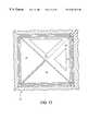
- FIG. 1is an exploded graphical representation of a hexagon shutter assembly according to the present invention
- FIG. 2Ais a close-up view of a shutter segment of the shutter assembly of FIG. 1 in a horizontal position
- FIG. 2Bis a representation of the shutter segment of FIG. 2A in a collapsed position
- FIG. 2Cdepicts another embodiment for a shutter segment of a shutter assembly according to the present invention.
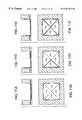
- FIGS. 3A, 3 Bdepict a cross-sectional view and the related top view of a square shutter assembly according to the present invention wherein the shutter is closed;
- FIGS. 3C, 3 Dshow a cross-sectional view of the shutter assembly shown in FIGS. 3A, 3 B and a corresponding top view wherein the shutter is open;
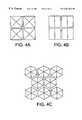
- FIGS. 4A-4Cdepict varying shutter assembly geometries
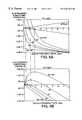
- FIG. 5Aprovides a graphical representation of spring torque and electro-static bias torque vs. deflection angle with no address voltage
- FIG. 5Bis a graphical representation of stored potential energy vs. deflection angle with no address voltage
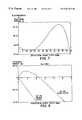
- FIG. 6Asets out a graphical representation of electrostatic and restoring torque at varying bias voltages and an address voltage applied
- FIG. 6Bis a graphical representation of total potential energy for an embodiment of the present invention at various bias voltages and an address voltage applied;
- FIG. 7graphically represents one example of a sub-threshold bias voltage having a maximum undesirable stable position at 13°;
- FIGS. 8A-8Bdepict a cross-sectional view and corresponding top view of two shutter assemblies according to the present invention.
- FIG. 9is a graphical representation of energy vs. angle curves for shutter assemblies for the present invention.
- FIG. 10Adepicts one embodiment of providing a color grey scale array wherein one color is provided per an individual shutter assembly
- FIG. 10Bshows a further embodiment of color grey scale array in the time domain wherein a plurality of colors are provided for within a single shutter assembly
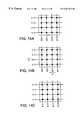
- FIGS. 11A-11Fillustrate varying positions of a shutter assembly operating in a space domain bistable grey scale environment wherein multiple segments per shutter assembly are depicted and which use a segmented address electrode;
- FIG. 12depicts a top view of a step-wise analogue grey scale with segmented address electrodes of different fill factors
- FIG. 13is graphical representation of a step-wise analogue bistable grey scale depicting address threshold voltage vs the address electrode fill factor
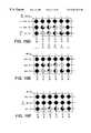
- FIGS. 14A-14Cillustrate a passive matrix addressing scheme
- FIGS. 15A-15Care depictions assisting in the understanding of a addressing scheme according to the present invention.
- FIGS. 16A-16Fillustrate additional concepts of the addressing scheme according to the present invention.
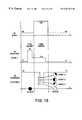
- FIG. 17is an illustration of signal lines according to the addressing schemes of FIGS. 16A-16F.
- FIG. 18shows signal lines for a further addressing scheme according to the present invention.
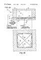
- FIG. 1illustrates a hexagon shutter assembly A
- FIGS. 3A-3Dillustrate a square shutter assembly A′ constructed in a stack layer formation according to the teachings of the present invention. It is to be understood that individual assemblies such as, assemblies A or A′ are formed with a large number of like assemblies to form a 2-D densely packed array display.
- FIG. 1is directed to a hexagon configuration and FIGS. 3A-3D are concerned with a square configuration, they are both constructed in accordance with similar procedures.
- FIG. 1is shown with its opening or upper surface pointed towards the bottom of the page, while the assembly shown in FIGS. 3A-3D depicts the opening or upper surface pointing towards the top of the page. Therefore, the following discussion is relevant to both designs.
- a top layer/film 10is a transparent face plate used for protection purposes and can be thin glass, a laminated polymer film or other transparent material.
- a first layer down from top layer/film 10is a conductive layer (or insulator coated with a conductive coating) 12 patterned with vertical sidewalls 14 to form cavities 15 , which in this embodiment have an aspect ratio>0.5 (depth ⁇ half the width).
- cavity 15is not required to have the above described aspect ratio, and will also function if sidewalls 14 are shorter than the length of the pixel size. Under this construction posts or otherwise known supports will be used to hold the top layer/film 10 .
- Conductive layer 12is common to all pixels, i.e. electrically not pixilated, and only one electrical terminal 16 (e.g. FIG. 3A) is needed for an entire 2D array.
- Sidewalls 14 of conductive layer 12are optically reflective and coated with a thin insulating layer (e.g. oxide).
- a second film down in the stackis a thin conductive film (or insulator coated with a conductive coating) patterned in the shape of micro-electromechanical shutters 18 that is suspended near the bottom of cavity 15 by flexible members that give shutters 18 a rotational degree of freedom.
- shutter segments 20 of shutters 18are suspended with torsion springs or hinges 22 patterned out of the same film and in the same step as shutters 18 .
- the second film downi.e. shutters 18
- Shutters 18are also electrically insulated from conductive layer 12 that defines sidewalls 14 .
- each shutter segment 20is optically absorbing (black) and their back side optically reflective. It is to be appreciated, however, the front face (and a backside as well) could be made white, or any other color.
- a third film downis a thin spacer film (insulator) 26 , defining a small gap between the suspended shutters 18 and a bottom layer or backplate 28 .
- Bottom layer or backplate 28is an electrically insulating support plate that can carry pixilated RGB color filter films 30 overlaying column address electrode 24 and column address electrode lines 32 .
- backplate 28can be opaque and column address electrode 24 and lines 32 can be reflective metal.
- backplate 28needs to be optically transparent (e.g. glass), as well as column address electrode 24 and lines 32 .
- Row address lines 34provide a path for row address pulses.
- the present inventiondescribes how, even for structures designed for small angles, shutter segments 18 can be twisted more than 90° without breaking. If they're made from single crystal silicon, the lifetime should not be an issue at all for practical purposes because SCS shows no fatigue, creep or plastic deformation, but lifetime is an issue for polycrystalline or amorphous materials. It has been reported that such materials may have under similar loading conditions lifetimes on the order of 10 5 cycles (Poly, Al or Cr/Au). For these materials, torsion springs 22 need to be designed such that stress at 90° is below the fatigue limit or elastic stress limit. Such torsion springs should be longer and thinner than single crystal silicon.
- FIG. 2Cillustrates a shutter segment 20 ′ with a torsion spring 22 ′ according to another embodiment of the present invention.
- Shutter segment 20 ′incorporates a longer torsion spring 22 ′ into a limited pixel area by using folded beams with one or multiple turns.
- Shutter segments 20 ′ according to this configurationare physically robust, in terms of handleability of the display, because they're single side clamped structures, not double side clamped and therefore immune to induced tensile or compressive stress.
- shutter assembly AThe operational principles of shutter assembly A will now be discussed in connection with situations where, a) no voltage is applied, b) a bias voltage is applied, and c) an address voltage and a bias voltage are applied.
- the latter positionis the desirable bias condition for operation of shutter assembly A and requires a DC bias ‘Vb’ to be applied beyond a certain critical threshold ‘Vbc’.
- FIGS. 5A-5Bshow an example of modeling (a 1 st order analytical) for the torques and potential energy versus the deflection angle, and for increasing bias voltages Vb.
- Vbis not equal to zero (i.e. a bias voltage exists between shutter 18 and sidewalls 14 )
- an electrostatic torqueacts on shutter segments 20 in addition to the spring's restoring torque.
- the electrostatic torqueis small for small deflection angles ⁇ , but grows large rapidly with an increasing deflection angle (1/(90° ⁇ ) 2 function).
- the electrostatic torqueis equal to the restoring torque as shown by the intersection points in FIG. 5A, which corresponds to a local minimum or maximum in the potential energy curve of FIG. 5 B.
- a bias voltage of 50Vis applied, the electrostatic torque intercepts the restoring torque at ⁇ 2° and ⁇ 78°.
- a bias voltage and an address voltageis applied to shutter assembly A.
- Address electrode 24causes an additional electrostatic torque (address torque) to act on shutter 18 , one that counteracts the bias torque.
- an address voltage ‘Va’ beyond the thresholdis applied (e.g 5V) which holds shutters 18 in the horizontal state.
- an appropriate DC bias of, for example, 200Vis applied to sidewalls 14 .
- the DC biasis commonly applied to all shutter assemblies of an array, and therefore is only connected to one electrical terminal. At this point, addressing voltage ‘Va’ still keeps shutters 18 in their horizontal state.
- a new frameis started by removing bias voltage ‘Vb’, returning all shutters 18 to the horizontal state and restarting the cycle.
- Vbbias voltage
- a particular shutter addressing linecan be selectively reset by pulsing it with Vb, for a high voltage switching option.
- a third option for address selectionis described in connection with FIGS. 16, 17 and 18 , in following sections of the document.
- address threshold voltageis insensitive to variations in the dimensions of torsion springs 22 . Variations in width, length or thickness of torsion springs 22 do affect the spring constant (which corresponds to the slope of the curve labeled ‘Spring’ in FIG. 6 A), but this has very little effect on its intersection points with the electrostatic torque curves as depicted in FIG. 6B, which define whether or not shutter is stable in its horizontal state. This means the addressing is very robust. This can also be understood by realizing that in the horizontal state of the shutter, the tug of war is between the two electrostatic torques, not between an electrostatic torque and the spring's restoring torque, which is negligibly small for these small angles.
- torsion spring 22does need to meet is that its spring constant needs to be sufficiently low to keep the bias threshold voltage (e.g. 1400V curve in FIG. 5A) at reasonable levels.
- FIG. 7details an example of what happens when an address voltage ‘Va’ is removed under sub-threshold bias conditions. When the address voltage is removed, shutters 18 find a stable position at 13° deflection instead of 90°. Robustness in this respect is easily achieved by respecting a safety margin in the applied bias voltage (e.g. 175V or 200V instead of 140V in FIG. 5 A). This makes achieving appropriate bias insensitive to variations in the spring constants as well.
- FIGS. 8A-8Bare conceptual sketches for an embodiment of shutter assembly A′′ configured in Single Crystal Silicon (SCS).
- SCSSingle Crystal Silicon
- Shutter assembly A′′consists of 3 wafers, 2 glass and one SOI silicon (Silicon On Insulator).
- Bottom glass wafer 40carries the ITO or Al column address electrodes 42 and pixilated color filters (R,G,B) 44 .
- Top glass wafer 46is unpatterned and is provided for protection purposes.
- Middle wafer 48is a SOI wafer, i.e. Si substrate with a silicon oxide layer buried underneath a thin single crystal silicon top layer.
- top wafer 46is made equal to the desired thickness of the torsion springs 50 and shutter segments 52 .
- RIEReactive Ion Etch
- the substrateshave a thickness not much larger than half the pixel width (unless the reflectivity of the sidewalls is very high, in which case the viewing angle and contrast ratio may not be affected very much by having ‘deeper’ pixels). Also, as previously discussed, shorter sidewalls may also be formed.
- a CVD oxideis deposited on the front side of the wafer and patterned to provide an appropriate space layer 56 .
- Very thin coats of metals or oxidescan be used to tailor the optical reflection/absorption/opacity (e.g. 300 ⁇ a1 for >80% reflectivity).
- the membraneis perforated in the shape of the shutters, the torsion springs 50 , anchor points 58 and row/row isolation trenches 60 .
- the layersare assembled e.g. using EPON adhesive wafer bonding process developed for TIJ (Thermal InkJet) or other known bonding process. Additionally, other silicon fabrication approaches, polysilicon on glass approaches, as well as the use of lamination based polymer approaches, could also be used.
- the values presentedare for a square 200 ⁇ m wide 2-segment shutter assembly A of the shutter assembly array, such as depicted in FIG. 4 B.
- the width of one shutter segment 20is 100 ⁇ m, its length 200 ⁇ m and its thickness 0.75 ⁇ m.
- the torsion springs 22are 180 ⁇ m long, 2 ⁇ m wide and 0.75 ⁇ m thick.
- the air gap between shutter 18 and address electrode 32is 1.5 ⁇ m and the fill factor of the address electrode is 1.
- a fill factoris defined as the area of the electrode relative to the shutter area.
- the address threshold voltageis 4V
- the 1 st mode resonance frequencyis on the order of 12 kHz
- the stress marginis approximately 12 ⁇ (maximum stress in the torsion springs 12 times below the yield strength).
- FIG. 9shows the corresponding energy vs. angle curve, for an address voltage of 6V.
- a color display according to the present inventioncan be achieved in a number of ways, two of which are shown in FIGS. 10A-10B.
- FIG. 10Aproposes one color filter per pixel (RGB pixilated polymer coatings).
- these filterswould be reflective filters or transmissive filters on top of a reflective back surface.
- thesewould be transmissive filters on top of a transparent back surface.
- FIG. 10Bproposes having one color filter per shutter segment, i.e. all RGB filters in each pixel. This approach would allow the pixels to be larger (for the same effective display resolution), relaxing various fabrication aspects.
- Greyscalecan be achieved in the space-domain and/or the time domain.
- FIGS. 10A-10Bone color per pixel and multiple segments per pixel, it is possible to also segment the underlying address electrodes as illustrated in FIGS. 11A-11E.
- the address electrodesbeing conductors supported by a substrate. It is noted that in FIGS. 11A-11F the black triangles 200 move and the white triangles 206 are static. If the address electrode segments have a different area (different fill factor, defined as the ratio of the address electrode segment and the shutter segment areas), the different shutter segments 20 of shutter 18 switch at different address threshold voltages ‘Va’, even if they are electrically connected to the same address line.
- FIG. 13is a simulated curve of the address threshold voltage as function of the address electrode fill factor. It uses the conditions and dimensions as in Table 1 A. It is assumed in this graph that the address segment is centered under its shutter segment 20 , as shown in FIG. 12 . All silicon shutters are identical, only the underlying address electrodes that are patterned into capacitor plates are of different areas. The required address threshold is a parabolic function of the fill factor. The example in FIG. 13 shows how, for example, 6 bistable greyscale levels are obtained in a hexagonal shutter assembly, with thresholds from 4 to 9 volts, spaced 1 volt apart, and that the required geometric fill factors of the 6 electrode segments would have to be from 1 down to 0.16.
- bistable greyscaleis achieved essentially for free. It will be appreciated that a bistable greyscale display is compatible with a passive matrix addressing scheme which has been developed by the inventors and which is described more fully below.
- a different approach to greyscale displayis to exploit the high bandwidth of the shutter assembly (e.g. resonance in the order of 10 kHz or higher) to achieve greyscale in the time domain.
- the shutter assemblye.g. resonance in the order of 10 kHz or higher
- greyscalein the time domain.
- the eye averages the fast switching and the overall brightness appearance (greyscale) of the pixelis proportional to how many of the time increments within the video frame the shutters were in the ‘bright’ state versus in the ‘dark’ state.
- time-domain greyscaleis increased power consumption, i.e. AC charge/discharge current.
- a line-reset schemeneeds to be used instead of a 2D frame reset. This is possible in a passive matrix using HV reset pulses on the shutter lines, as is more fully described below.
- Passive matrix addressing of an array of shutter assemblies Acan be accomplished with a sequence as in FIGS. 14A-14C (e.g. 4 ⁇ 4 array).
- the horizontal address linesrepresent the row electrodes (the different rows of shutters are electrically isolated; the shutters within each row are electrically connected to each other) and the vertical lines represent the column electrodes (the different columns of address electrodes on the backplate are electrically isolated, and the electrodes within each column are connected.)
- FIG. 14AIn a second alternative for address switching, attention is directed to FIG. 14A, wherein the starting point of the addressing is with all rows at 0 V and all columns at a voltage slightly above address threshold voltage ‘Vta’, e.g. 5 V.
- the bias voltage ‘Vb’ applied to all sidewalls 14is above bias threshold voltage ‘Vbt’, e.g. 200V.
- Vbtbias threshold voltage
- both its row and column linesare pulsed down to ⁇ Vt, while all other columns remain at +Vt and all other rows at 0 V.
- the shutter segments in the pixel to be switchednow only see bias voltage ‘Vb’ and switches to the 90° position (0V across the shutter and the address electrode below).
- the other pixelseither see ‘Vt’ or ‘2Vt’ between their shutters 18 and address electrodes 32 , both in excess of the address threshold voltage ‘Vta’. These will therefore stay in the dark state as shown in FIG. 14 B.
- +Vtcould be added to all lines, which would result in avoiding switching to negative voltages.
- the minimum duration of the address pulsesis defined by the time required to bring the shutters beyond the local maximum in the potential energy curve. For example, in FIG. 9, to bring the shutters beyond 2° deflection angle. This takes 17 ⁇ s under the conditions in Table 1A (200 ⁇ m pixels) and about 4 ⁇ s in Table 1B (100 ⁇ m pixels). Under the ‘2D frame reset’ scenario, the entire 2D array is reset to start a new frame (by momentarily resetting the bias voltage) and a ‘holding’ time must therefore be built in to avoid lines written later to appear dimmer than lines written earlier.
- the corresponding frame rate in Table 1Ais about 20 frames per second (for a display with 320 lines at 200 ⁇ m per line) and about 40 frames per second in Table 1B (for a VGA display sized with 650 lines at 100 ⁇ m per line). These frame rates appear acceptable for small display (i.e. PDR/PDA) type applications.
- a line reset schemecan be used. The line-reset scheme does not require any changes in the display hardware geometry (i.e. FIGS. 1-3B still apply), but can use a high voltage reset pulse on the shutter lines. The passive matrix scheme still works as well, even in combination with the bistable grey scale.
- the voltage on the lineis momentarily pulsed to the bias voltage (e.g. the 175V in Table 1A).
- the bias voltagee.g. the 175V in Table 1A.
- the shutters in this line that were in the ‘down’ state prior to the reset pulsewill stay in the ‘down’ state because they now see even a much larger voltage across their address capacitor (parallel plate capacitor).
- the ones that were in the ‘up’ state on the other handreset to the ‘down’ state because the voltage between shutter 18 and sidewall 14 is zero during the reset pulse (i.e. both at 175V). This allows them to be ‘captured’ again by the address field.
- Line resetallows selective refreshing of parts of the display. This allows for higher speeds, and reduces the AC power consumption.
- FIGS. 15A-15CA display implementing an array of shutter assemblies A according to the present invention can be addressed by a variety of schemes.
- a preferred manneris depicted in FIGS. 15A-15C.
- This particular addressing schemeis a passive matrix type compatible with bistable grey scale (multiple shutter segments per pixel) and requires only low voltage (e.g. ⁇ 20V) switches on the rows and columns.
- One discrete high-voltage switche.g. 150V
- FIG. 15Arepresents a schematic cross-section of half a pixel
- FIG. 15Brepresents a schematic top view of a 3 ⁇ 6 array
- FIG. 15Cis a hysteresis diagram showing a scenario with 4 shutter segments per pixel (e.g. 4 triangles forming a square pixel).
- FIGS. 16A-16Fillustrate an example of a 3 ⁇ 6 array being addressed.
- FIG. 17is a timing diagram for this example. The foregoing figures are explained in more detail in the following discussion.
- FIG. 15Ais a schematic cross-section of half a shutter assembly 70 , the torsionally suspended shutters 72 are electrically connected into rows (the voltage on a row is denoted Vs, i.e. V-shutter).
- Address capacitor plates on backplane 74are electrically connected into columns (the voltage on a column is denoted as Va, i.e. Vaddress).
- Sidewalls 76 of the body 78 for all shutter assemblies 70are electrically connected, i.e. the ‘body’ of the array (the bias voltage on the body is denoted as Vb, i.e. Vbody or Vbias).
- the position of the shutteris determined by a ‘tug-of-war’ between two electrostatic fields.
- the field between the shutter and the body(determined by Vb ⁇ Vs) pulls the shutter towards the vertical ( ⁇ 90°), while the field between the shutter and the address electrode on the backplane (determined by the voltage Vs ⁇ Va) pulls the shutter towards the horizontal ( ⁇ 0°, or even slightly negative angle, FIG. 15 A).
- the state of the shutteris determined by its previous state and by the magnitude of (Vs ⁇ Va) vs. (Vb ⁇ Vs).
- the voltage (Vs ⁇ Va)is the difference between the row and column voltages.
- the voltage (Vb ⁇ Vs)is the difference between the body voltage (Vb) and the row voltage (Vs) (see FIG. 15 B).
- FIG. 15Cshows an example of a shutter-state hysteresis loop.
- the horizontal axisrepresents (Vs ⁇ Va) (row minus column); the vertical axis represents the state of 4 individual shutter segments in a square pixel (vertical, ⁇ 90° or horizontal ⁇ 0°).
- the 4 address electrodes on the backplane, corresponding to each of the 4 shutter segments,have a different area and the address threshold voltage is therefore different for the 4 segments. The foregoing has previously been discussed in connection with FIGS. 11A-11E.
- the first shutter segmentflips from the horizontal into the vertical position ( ⁇ :0 ⁇ 90°) in the presence of the bias voltage on the body, as soon as the voltage (Vs ⁇ Va, i.e. row/column difference) is brought below 6 V, the second shutter flips when (Vs ⁇ Va) ⁇ 5V, the third when (Vs ⁇ Va) ⁇ 4V and the forth one when (Vs ⁇ Va) ⁇ 3V. If (Vs ⁇ Va) ⁇ 6V, all four shutters are in the horizontal state (i.e. black).
- a 4-segment shutteris potentially capable of 5 levels of grey scale (black, grey1, grey2, grey3, white).
- An important characteristic of the addressing hysteresis loopis also that typically 150V bias is required to flip the shutters vertical, but much less voltage is required to keep shutter segments vertical, because the sidewall/shutter capacitance is much larger in the vertical state. This means that the bias voltage on the body of the array can be brought down to 20V or so (from 150V) after a line is addressed, without the vertical shutter segments flipping back into their horizontal position. This property will be used to avoid high voltage switches on rows or columns as will be discussed below.
- FIGS. 16A-16Fillustrates an addressing example, and FIG. 17 a set of segments on a time line.
- the figurescorrespond to the example hysteresis loop in FIG. 15 C.
- FIG. 16Ashows a 3 ⁇ 6 array in a quiescent and dark state, all shutters horizontal (black).
- the bias voltage on the bodyis e.g. 20V
- the rows (shutter segments)are held slightly below 6V
- the columns (address electrodes)are held at ⁇ 6V (note that all voltages can be shifted up to make everything unipolar, but the bipolar scheme seems to be clearer for explanation purposes).
- the bias voltage on the bodycan be brought back down to 20V.
- a holding voltage of 20Vpossibly lower is sufficient to keep all shutters in their addressed state. This is again a quiescent state (FIG. 16 C).
- the only power consumptionis due to leakage current.
- the 150V pulses on the bodycan be accomplished with a switched LC circuit. This would allow for the recovery of charge on the body-to-shutter capacitances, rather than dissipating that charge. This charge is considerable because of the high voltage on the body.
- the main source of AC power consumptionis associated with charging and discharging of this capacitor.
- FIG. 16Dshows another row (row3) being addressed in a similar way (a different bit pattern though).
- row3previously addressed row2 is unaffected because the row/column difference on all its pixels is more than 6V (i.e. more than required for the first segment of a pixel to flip up; see hysteresis loop). It is to be noted that in all rows other than the row being addressed at any particular time, ‘down’ segments stay ‘down’ and ‘up’ segments stay ‘up’.
- FIG. 16Eis again a quiescent state, where the body is brought back to 20V after addressing of row3 and all rows are back at 6+ ⁇ and all columns at ⁇ 6V.
- FIG. 16 F and FIG. 17finally show the reset of a particular row (row2).
- ‘resetting’ a rowmeans bringing its ‘up’ segments back ‘down’)
- the row voltageis pulsed to 20V (or even somewhat lower) while the body voltage is also at 20V. All other rows remain at 6+ ⁇ and all columns e.g. at ⁇ 6V.
- Bringing the row to be reset to the same voltage as the bodydischarges its sidewall/shutter capacitor and the restoring force of the torsion spring (plus voltage on the address capacitor, i.e. column) brings the shutter segments back to their horizontal position, i.e. the row is now reset.
- the schemecan be unipolar (by shifting everything 6V up) and the reset pulse could immediately be followed by the address voltage, etc . . . .
- the one most suitedwill be determined in the light of the driver circuitry or other parameters.
- a drive scheme attractive for practical implementationis shown in FIG. 18 . It is a unipolar scheme where the reset pulse immediately precedes the write pulse (rows), where the body is kept at 14V in the quiescent state and momentarily brought to 150V during the write step. The quiescent voltage on the rows is 0V and 12V on the columns. During the addressing step, the row is brought up to 3 ⁇ V and the columns are brought down to 9V, 8V, 7V or 6V (grey scale values).
- a virtue of the proposed display systemis its bi-stability and hence the lack of DC power consumption, making it particularly suitable for battery powered, portable devices such as PDRs (Personal Document Reader).
- PDRsPersonal Document Reader
- In the stable statethere is a holding field, but no current flow (except negligible leakage currents), i.e. a miniature battery can last practically indefinitely in this state.
- the consumption of poweroccurs only during pixel switching, i.e. due to charging/discharging of pixel capacitors. By far the largest charge is associated with charging the shutter-to-sidewall capacitance in the bright state (shutter vertical).
- the power consumptionis therefore proportional to the refresh rate and also to the shutter to sidewall capacitance, the area of the display and its fill factor and to the square of the bias voltage.
- the power consumptionwas calculated for a few PDR scenarios and tabulated in Table 2, as well as the corresponding lifetime of a AAA-size alkaline battery (assumed 50 Whr/lb battery capacity).
- the fill factorcan be 90% (20:1 aspect ratio etch).
- the cavitiesconsist of multiple corner cube reflectors, which provide for high reflection efficiency.
- the sidewalls of an STS RIE etched silicon cavityare relatively flat and reflective, a thin A1 (300 ⁇ ) coat can easily bring the reflectivity well above 80% for all visible wavelengths. Also, the viewing angle will be very wide as the reflectivity of the sidewalls and shutter backsides is better than 80%.
- the shutter assembly described aboveappears readily feasible in single crystal silicon with the current state of micromachining technology, e.g. for 2.5 ⁇ 3′′ PDR displays.
- the conceptsare scalable to large area displays.
- the display arrays according to the present inventioncan also be fabricated using polysilicon on glass technology or plastic film lamination processing.
Landscapes
- Physics & Mathematics (AREA)
- Engineering & Computer Science (AREA)
- General Physics & Mathematics (AREA)
- Optics & Photonics (AREA)
- Computer Hardware Design (AREA)
- Theoretical Computer Science (AREA)
- Multimedia (AREA)
- Signal Processing (AREA)
- Devices For Indicating Variable Information By Combining Individual Elements (AREA)
- Control Of Indicators Other Than Cathode Ray Tubes (AREA)
- Mechanical Light Control Or Optical Switches (AREA)
Abstract
Description
| TABLE 1A | ||||
| Shutter | Torsion spring | |||
| Length | L | 2.00E-04 | [m] Half length | |||
| TL 1.80E-04 | [m] | |||||
| Width | W | 1.00E-04 | [m] Width | |||
| TW 2.00E-06 | [m] | |||||
| Hinge gap g | 7.00E-06 | [m] Thickness | TT | |||
| 7.50E-07 [m] | ||||||
| Address electrode | Material | |
| Airgap | d 1.50E-06 [m] | Shear-modulus | |
| G 6.40E + 10 [Pa] | |||
| Fill factor | FF 1 [−] | Density | |
| Rho 2.30E + 03 [kg/mΛ3] | |||
| (area) | Yield strength | Tmax | |
| 7.00E + 09 [Pa] | |||
| Bias voltage | Address voltage | |||
| Top | VB | 175 | [V] Column (Si) | |||
| VA1 0 | [V] | |||||
| Rpw (ITO) | VA2 6 | |||||
| [V] | ||||||
| Outputs: |
| Resonance | |||
| frequency | Fn 1.202E + 04 | [Hz] | |
| Stress margin | Tmax/T 11.7 | [X] | |
| Address | |||
| threshold | Vt 4.0 | [V] | Switching time: |
| Ts 17E-06 [s] | |||
| Frame rate: | |||
| 19 [fr/s] |
| 320Li (=2.5″), 10 × hold | |
| time | |
| TABLE 1B | ||||
| Shutter | Torsion spring | |||
| Length | L | 1.00E-04 | [m] Half length | |||
| TL 9.00E-05 | [m] | |||||
| Width | W | 5.00E-05 | [m] Width | |||
| TW 1.50E-06 | [m] | |||||
| Hinge gap g | 6.00E-06 | [m] Thickness | TT | |||
| 3.50E-07 [m] | ||||||
| Address electrode | Material | |
| Airgap | d 1.00E-06 [m] | Shear-modulus | |
| G 6.40E + 10 [Pa] | |||
| Fill factor | FF 1 [−] | Density | |
| Rho 2.30E + 03 [kg/mΛ3] | |||
| (area) | Yield strength | Tmax | |
| 7.00E + 09 [Pa] | |||
| Bias voltage | Address voltage | |||
| Top | VB | 200 | [V] Column (Si) | |||
| VA1 0 | [V] | |||||
| Rpw (ITO) | VA2 6 | |||||
| [V] | ||||||
| Outputs: |
| Resonance | |||
| frequency | Fn 2.811E + 04 | [Hz] | |
| Stress margin | Tmax/T 8.1 | [X] | |
| Address | |||
| threshold | Vt 5.6 | [V] | Switching time: |
| Ts 3.90E-06 | [s] | ||
| Frame rate: | |||
| 40 [fr/s] |
| 640Li, 10 × hold time | |
| TABLE 2 | |
| Use: | |
| hours/days | |
| (10 continuous) | Pwr: AAA Battery |
| Video: 40 | 10 | mW | 31 | days |
| continuous, 10 hr/day, | ||||
| 7 days/week | ||||
| Web browsing: Hz frame rate | 1.25 | 9 | ||
| months | ||||
| Document reading: 1 Hz frame rate | 0.25 | 3 | years | |
| 13824 colors (+2 bit time domain grey): | 30 | 10 | ||
| 32 Hz frame, 128 Hz pixel | ||||
Claims (24)
Priority Applications (2)
| Application Number | Priority Date | Filing Date | Title |
|---|---|---|---|
| US09/326,876US6201633B1 (en) | 1999-06-07 | 1999-06-07 | Micro-electromechanical based bistable color display sheets |
| JP2000159277AJP4602515B2 (en) | 1999-06-07 | 2000-05-30 | Ultra-precision electromechanical shutter assembly and forming method thereof |
Applications Claiming Priority (1)
| Application Number | Priority Date | Filing Date | Title |
|---|---|---|---|
| US09/326,876US6201633B1 (en) | 1999-06-07 | 1999-06-07 | Micro-electromechanical based bistable color display sheets |
Publications (1)
| Publication Number | Publication Date |
|---|---|
| US6201633B1true US6201633B1 (en) | 2001-03-13 |
Family
ID=23274108
Family Applications (1)
| Application Number | Title | Priority Date | Filing Date |
|---|---|---|---|
| US09/326,876Expired - LifetimeUS6201633B1 (en) | 1999-06-07 | 1999-06-07 | Micro-electromechanical based bistable color display sheets |
Country Status (2)
| Country | Link |
|---|---|
| US (1) | US6201633B1 (en) |
| JP (1) | JP4602515B2 (en) |
Cited By (255)
| Publication number | Priority date | Publication date | Assignee | Title |
|---|---|---|---|---|
| US20020075555A1 (en)* | 1994-05-05 | 2002-06-20 | Iridigm Display Corporation | Interferometric modulation of radiation |
| US20040058532A1 (en)* | 2002-09-20 | 2004-03-25 | Miles Mark W. | Controlling electromechanical behavior of structures within a microelectromechanical systems device |
| US20040209192A1 (en)* | 2003-04-21 | 2004-10-21 | Prime View International Co., Ltd. | Method for fabricating an interference display unit |
| US20040240032A1 (en)* | 1994-05-05 | 2004-12-02 | Miles Mark W. | Interferometric modulation of radiation |
| US20040263944A1 (en)* | 2003-06-24 | 2004-12-30 | Miles Mark W. | Thin film precursor stack for MEMS manufacturing |
| US20050036095A1 (en)* | 2003-08-15 | 2005-02-17 | Jia-Jiun Yeh | Color-changeable pixels of an optical interference display panel |
| US20050046948A1 (en)* | 2003-08-26 | 2005-03-03 | Wen-Jian Lin | Interference display cell and fabrication method thereof |
| US20050046922A1 (en)* | 2003-09-03 | 2005-03-03 | Wen-Jian Lin | Interferometric modulation pixels and manufacturing method thereof |
| US20050122560A1 (en)* | 2003-12-09 | 2005-06-09 | Sampsell Jeffrey B. | Area array modulation and lead reduction in interferometric modulators |
| US20050142684A1 (en)* | 2002-02-12 | 2005-06-30 | Miles Mark W. | Method for fabricating a structure for a microelectromechanical system (MEMS) device |
| US20050168431A1 (en)* | 2004-02-03 | 2005-08-04 | Clarence Chui | Driver voltage adjuster |
| US20050167567A1 (en)* | 2004-01-23 | 2005-08-04 | Fernandez Jose A. | Device and method for pixel generation, and apparatus and method for image projection |
| US20050195468A1 (en)* | 2004-03-05 | 2005-09-08 | Sampsell Jeffrey B. | Integrated modulator illumination |
| US20050212738A1 (en)* | 2004-03-06 | 2005-09-29 | Brian Gally | Method and system for color optimization in a display |
| US20050249966A1 (en)* | 2004-05-04 | 2005-11-10 | Ming-Hau Tung | Method of manufacture for microelectromechanical devices |
| US20050250235A1 (en)* | 2002-09-20 | 2005-11-10 | Miles Mark W | Controlling electromechanical behavior of structures within a microelectromechanical systems device |
| US20050247477A1 (en)* | 2004-05-04 | 2005-11-10 | Manish Kothari | Modifying the electro-mechanical behavior of devices |
| US20050254115A1 (en)* | 2004-05-12 | 2005-11-17 | Iridigm Display Corporation | Packaging for an interferometric modulator |
| US6972881B1 (en) | 2002-11-21 | 2005-12-06 | Nuelight Corp. | Micro-electro-mechanical switch (MEMS) display panel with on-glass column multiplexers using MEMS as mux elements |
| US20050277277A1 (en)* | 2000-10-13 | 2005-12-15 | Taiwan Semiconductor Manufacturing Company, Ltd. | Dual damascene process |
| US20050286114A1 (en)* | 1996-12-19 | 2005-12-29 | Miles Mark W | Interferometric modulation of radiation |
| US20050286113A1 (en)* | 1995-05-01 | 2005-12-29 | Miles Mark W | Photonic MEMS and structures |
| US20060001942A1 (en)* | 2004-07-02 | 2006-01-05 | Clarence Chui | Interferometric modulators with thin film transistors |
| US20060007517A1 (en)* | 2004-07-09 | 2006-01-12 | Prime View International Co., Ltd. | Structure of a micro electro mechanical system |
| US20060024880A1 (en)* | 2004-07-29 | 2006-02-02 | Clarence Chui | System and method for micro-electromechanical operation of an interferometric modulator |
| US20060044246A1 (en)* | 2004-08-27 | 2006-03-02 | Marc Mignard | Staggered column drive circuit systems and methods |
| US20060044928A1 (en)* | 2004-08-27 | 2006-03-02 | Clarence Chui | Drive method for MEMS devices |
| US7012726B1 (en) | 2003-11-03 | 2006-03-14 | Idc, Llc | MEMS devices with unreleased thin film components |
| US20060057754A1 (en)* | 2004-08-27 | 2006-03-16 | Cummings William J | Systems and methods of actuating MEMS display elements |
| US20060066864A1 (en)* | 2004-09-27 | 2006-03-30 | William Cummings | Process control monitors for interferometric modulators |
| US20060067651A1 (en)* | 2004-09-27 | 2006-03-30 | Clarence Chui | Photonic MEMS and structures |
| US20060067644A1 (en)* | 2004-09-27 | 2006-03-30 | Clarence Chui | Method of fabricating interferometric devices using lift-off processing techniques |
| US20060067648A1 (en)* | 2004-09-27 | 2006-03-30 | Clarence Chui | MEMS switches with deforming membranes |
| US20060067643A1 (en)* | 2004-09-27 | 2006-03-30 | Clarence Chui | System and method for multi-level brightness in interferometric modulation |
| US20060067600A1 (en)* | 2004-09-27 | 2006-03-30 | Gally Brian J | Display element having filter material diffused in a substrate of the display element |
| US20060065622A1 (en)* | 2004-09-27 | 2006-03-30 | Floyd Philip D | Method and system for xenon fluoride etching with enhanced efficiency |
| US20060066543A1 (en)* | 2004-09-27 | 2006-03-30 | Gally Brian J | Ornamental display device |
| US20060067649A1 (en)* | 2004-09-27 | 2006-03-30 | Ming-Hau Tung | Apparatus and method for reducing slippage between structures in an interferometric modulator |
| US20060066936A1 (en)* | 2004-09-27 | 2006-03-30 | Clarence Chui | Interferometric optical modulator using filler material and method |
| US20060066594A1 (en)* | 2004-09-27 | 2006-03-30 | Karen Tyger | Systems and methods for driving a bi-stable display element |
| US20060066598A1 (en)* | 2004-09-27 | 2006-03-30 | Floyd Philip D | Method and device for electrically programmable display |
| US20060066504A1 (en)* | 2004-09-27 | 2006-03-30 | Sampsell Jeffrey B | System with server based control of client device display features |
| US20060066541A1 (en)* | 2004-09-27 | 2006-03-30 | Gally Brian J | Method and device for manipulating color in a display |
| US20060066597A1 (en)* | 2004-09-27 | 2006-03-30 | Sampsell Jeffrey B | Method and system for reducing power consumption in a display |
| US20060066560A1 (en)* | 2004-09-27 | 2006-03-30 | Gally Brian J | Systems and methods of actuating MEMS display elements |
| US20060066542A1 (en)* | 2004-09-27 | 2006-03-30 | Clarence Chui | Interferometric modulators having charge persistence |
| US20060067652A1 (en)* | 2004-09-27 | 2006-03-30 | Cummings William J | Methods for visually inspecting interferometric modulators for defects |
| US20060067633A1 (en)* | 2004-09-27 | 2006-03-30 | Gally Brian J | Device and method for wavelength filtering |
| US20060066599A1 (en)* | 2004-09-27 | 2006-03-30 | Clarence Chui | Reflective display pixels arranged in non-rectangular arrays |
| US20060067642A1 (en)* | 2004-09-27 | 2006-03-30 | Karen Tyger | Method and device for providing electronic circuitry on a backplate |
| US20060066937A1 (en)* | 2004-09-27 | 2006-03-30 | Idc, Llc | Mems switch with set and latch electrodes |
| US20060065436A1 (en)* | 2004-09-27 | 2006-03-30 | Brian Gally | System and method for protecting microelectromechanical systems array using back-plate with non-flat portion |
| US20060065043A1 (en)* | 2004-09-27 | 2006-03-30 | William Cummings | Method and system for detecting leak in electronic devices |
| US20060066863A1 (en)* | 2004-09-27 | 2006-03-30 | Cummings William J | Electro-optical measurement of hysteresis in interferometric modulators |
| US20060066932A1 (en)* | 2004-09-27 | 2006-03-30 | Clarence Chui | Method of selective etching using etch stop layer |
| US20060066559A1 (en)* | 2004-09-27 | 2006-03-30 | Clarence Chui | Method and system for writing data to MEMS display elements |
| US20060067641A1 (en)* | 2004-09-27 | 2006-03-30 | Lauren Palmateer | Method and device for packaging a substrate |
| US20060066856A1 (en)* | 2004-09-27 | 2006-03-30 | William Cummings | Systems and methods for measuring color and contrast in specular reflective devices |
| US20060066595A1 (en)* | 2004-09-27 | 2006-03-30 | Sampsell Jeffrey B | Method and system for driving a bi-stable display |
| US20060067650A1 (en)* | 2004-09-27 | 2006-03-30 | Clarence Chui | Method of making a reflective display device using thin film transistor production techniques |
| US20060066596A1 (en)* | 2004-09-27 | 2006-03-30 | Sampsell Jeffrey B | System and method of transmitting video data |
| US20060066876A1 (en)* | 2004-09-27 | 2006-03-30 | Manish Kothari | Method and system for sensing light using interferometric elements |
| US20060067646A1 (en)* | 2004-09-27 | 2006-03-30 | Clarence Chui | MEMS device fabricated on a pre-patterned substrate |
| US20060066938A1 (en)* | 2004-09-27 | 2006-03-30 | Clarence Chui | Method and device for multistate interferometric light modulation |
| US20060066557A1 (en)* | 2004-09-27 | 2006-03-30 | Floyd Philip D | Method and device for reflective display with time sequential color illumination |
| US20060066601A1 (en)* | 2004-09-27 | 2006-03-30 | Manish Kothari | System and method for providing a variable refresh rate of an interferometric modulator display |
| US20060066600A1 (en)* | 2004-09-27 | 2006-03-30 | Lauren Palmateer | System and method for display device with reinforcing substance |
| US20060066503A1 (en)* | 2004-09-27 | 2006-03-30 | Sampsell Jeffrey B | Controller and driver features for bi-stable display |
| US20060065366A1 (en)* | 2004-09-27 | 2006-03-30 | Cummings William J | Portable etch chamber |
| US20060077152A1 (en)* | 2004-09-27 | 2006-04-13 | Clarence Chui | Device and method for manipulation of thermal response in a modulator |
| US20060077515A1 (en)* | 2004-09-27 | 2006-04-13 | Cummings William J | Method and device for corner interferometric modulation |
| US20060077518A1 (en)* | 2004-09-27 | 2006-04-13 | Clarence Chui | Mirror and mirror layer for optical modulator and method |
| US20060077529A1 (en)* | 2004-09-27 | 2006-04-13 | Clarence Chui | Method of fabricating a free-standing microstructure |
| US20060077505A1 (en)* | 2004-09-27 | 2006-04-13 | Clarence Chui | Device and method for display memory using manipulation of mechanical response |
| US20060077149A1 (en)* | 2004-09-27 | 2006-04-13 | Gally Brian J | Method and device for manipulating color in a display |
| US20060077151A1 (en)* | 2004-09-27 | 2006-04-13 | Clarence Chui | Method and device for a display having transparent components integrated therein |
| US20060076311A1 (en)* | 2004-09-27 | 2006-04-13 | Ming-Hau Tung | Methods of fabricating interferometric modulators by selectively removing a material |
| US20060077528A1 (en)* | 2004-09-27 | 2006-04-13 | Floyd Philip D | Device and method for modifying actuation voltage thresholds of a deformable membrane in an interferometric modulator |
| US20060079098A1 (en)* | 2004-09-27 | 2006-04-13 | Floyd Philip D | Method and system for sealing a substrate |
| US20060077145A1 (en)* | 2004-09-27 | 2006-04-13 | Floyd Philip D | Device having patterned spacers for backplates and method of making the same |
| US20060076637A1 (en)* | 2004-09-27 | 2006-04-13 | Gally Brian J | Method and system for packaging a display |
| US20060079048A1 (en)* | 2004-09-27 | 2006-04-13 | Sampsell Jeffrey B | Method of making prestructure for MEMS systems |
| US20060077156A1 (en)* | 2004-09-27 | 2006-04-13 | Clarence Chui | MEMS device having deformable membrane characterized by mechanical persistence |
| US20060077514A1 (en)* | 2004-09-27 | 2006-04-13 | Sampsell Jeffrey B | System and method of reducing color shift in a display |
| US20060077507A1 (en)* | 2004-09-27 | 2006-04-13 | Clarence Chui | Conductive bus structure for interferometric modulator array |
| US20060076634A1 (en)* | 2004-09-27 | 2006-04-13 | Lauren Palmateer | Method and system for packaging MEMS devices with incorporated getter |
| US20060077393A1 (en)* | 2004-09-27 | 2006-04-13 | Gally Brian J | System and method for implementation of interferometric modulator displays |
| US20060077155A1 (en)* | 2004-09-27 | 2006-04-13 | Clarence Chui | Reflective display device having viewable display on both sides |
| US20060077524A1 (en)* | 2004-09-27 | 2006-04-13 | Lauren Palmateer | System and method for display device with end-of-life phenomena |
| US20060077527A1 (en)* | 2004-09-27 | 2006-04-13 | Cummings William J | Methods and devices for inhibiting tilting of a mirror in an interferometric modulator |
| US20060077122A1 (en)* | 2004-09-27 | 2006-04-13 | Gally Brian J | Apparatus and method for reducing perceived color shift |
| US20060077510A1 (en)* | 2004-09-27 | 2006-04-13 | Clarence Chui | System and method of illuminating interferometric modulators using backlighting |
| US20060077126A1 (en)* | 2004-09-27 | 2006-04-13 | Manish Kothari | Apparatus and method for arranging devices into an interconnected array |
| US20060077503A1 (en)* | 2004-09-27 | 2006-04-13 | Lauren Palmateer | System and method of providing MEMS device with anti-stiction coating |
| US20060077617A1 (en)* | 2004-09-27 | 2006-04-13 | Floyd Philip D | Selectable capacitance circuit |
| US20060077504A1 (en)* | 2004-09-27 | 2006-04-13 | Floyd Philip D | Method and device for protecting interferometric modulators from electrostatic discharge |
| US20060077523A1 (en)* | 2004-09-27 | 2006-04-13 | Cummings William J | Electrical characterization of interferometric modulators |
| US20060077508A1 (en)* | 2004-09-27 | 2006-04-13 | Clarence Chui | Method and device for multistate interferometric light modulation |
| US20060077521A1 (en)* | 2004-09-27 | 2006-04-13 | Gally Brian J | System and method of implementation of interferometric modulators for display mirrors |
| US20060077516A1 (en)* | 2004-09-27 | 2006-04-13 | Manish Kothari | Device having a conductive light absorbing mask and method for fabricating same |
| US20060077512A1 (en)* | 2004-09-27 | 2006-04-13 | Cummings William J | Display device having an array of spatial light modulators with integrated color filters |
| US20060103613A1 (en)* | 2004-09-27 | 2006-05-18 | Clarence Chui | Interferometric modulator array with integrated MEMS electrical switches |
| US20060103643A1 (en)* | 2004-09-27 | 2006-05-18 | Mithran Mathew | Measuring and modeling power consumption in displays |
| US20060177950A1 (en)* | 2005-02-04 | 2006-08-10 | Wen-Jian Lin | Method of manufacturing optical interferance color display |
| EP1693824A1 (en)* | 2005-02-18 | 2006-08-23 | Sony Deutschland GmbH | Shutter device for pixel element and pixel arrangement |
| US20060187191A1 (en)* | 2005-02-23 | 2006-08-24 | Pixtronix, Incorporated | Display methods and apparatus |
| US20060187531A1 (en)* | 2005-02-23 | 2006-08-24 | Pixtronix, Incorporated | Methods and apparatus for bi-stable actuation of displays |
| US20060187528A1 (en)* | 2005-02-23 | 2006-08-24 | Pixtronix, Incorporated | Methods and apparatus for spatial light modulation |
| US20060187190A1 (en)* | 2005-02-23 | 2006-08-24 | Pixtronix, Incorporated | Display methods and apparatus |
| US20060187530A1 (en)* | 2005-02-23 | 2006-08-24 | Pixtronix, Incorporated | Methods and apparatus for actuating displays |
| US20060187529A1 (en)* | 2005-02-23 | 2006-08-24 | Pixtronix, Incorporated | Display methods and apparatus |
| WO2006087219A1 (en)* | 2005-02-18 | 2006-08-24 | Sony Deutschland Gmbh | Shutter device for pixel element and pixel arrangement |
| US20060209012A1 (en)* | 2005-02-23 | 2006-09-21 | Pixtronix, Incorporated | Devices having MEMS displays |
| US7119945B2 (en) | 2004-03-03 | 2006-10-10 | Idc, Llc | Altering temporal response of microelectromechanical elements |
| US7123216B1 (en) | 1994-05-05 | 2006-10-17 | Idc, Llc | Photonic MEMS and structures |
| US20060250335A1 (en)* | 2005-05-05 | 2006-11-09 | Stewart Richard A | System and method of driving a MEMS display device |
| US20060250676A1 (en)* | 2005-02-23 | 2006-11-09 | Pixtronix, Incorporated | Light concentrating reflective display methods and apparatus |
| US20060250350A1 (en)* | 2005-05-05 | 2006-11-09 | Manish Kothari | Systems and methods of actuating MEMS display elements |
| US20060256039A1 (en)* | 2005-02-23 | 2006-11-16 | Pixtronix, Incorporated | Display methods and apparatus |
| US7138984B1 (en) | 2001-06-05 | 2006-11-21 | Idc, Llc | Directly laminated touch sensitive screen |
| US20060262380A1 (en)* | 1998-04-08 | 2006-11-23 | Idc, Llc A Delaware Limited Liability Company | MEMS devices with stiction bumps |
| US7142346B2 (en) | 2003-12-09 | 2006-11-28 | Idc, Llc | System and method for addressing a MEMS display |
| US20060277486A1 (en)* | 2005-06-02 | 2006-12-07 | Skinner David N | File or user interface element marking system |
| US20070002156A1 (en)* | 2005-02-23 | 2007-01-04 | Pixtronix, Incorporated | Display apparatus and methods for manufacture thereof |
| US7161730B2 (en) | 2004-09-27 | 2007-01-09 | Idc, Llc | System and method for providing thermal compensation for an interferometric modulator display |
| US7172915B2 (en) | 2003-01-29 | 2007-02-06 | Qualcomm Mems Technologies Co., Ltd. | Optical-interference type display panel and method for making the same |
| KR100687606B1 (en) | 2004-11-12 | 2007-02-27 | 한국과학기술원 | Light valve having a movable thin film and display device using the same |
| US20070053652A1 (en)* | 2005-09-02 | 2007-03-08 | Marc Mignard | Method and system for driving MEMS display elements |
| US20070058095A1 (en)* | 1994-05-05 | 2007-03-15 | Miles Mark W | System and method for charge control in a MEMS device |
| US20070096300A1 (en)* | 2005-10-28 | 2007-05-03 | Hsin-Fu Wang | Diffusion barrier layer for MEMS devices |
| US20070147688A1 (en)* | 2005-12-22 | 2007-06-28 | Mithran Mathew | System and method for power reduction when decompressing video streams for interferometric modulator displays |
| US20070170540A1 (en)* | 2006-01-18 | 2007-07-26 | Chung Won Suk | Silicon-rich silicon nitrides as etch stops in MEMS manufature |
| US20070177129A1 (en)* | 2006-01-06 | 2007-08-02 | Manish Kothari | System and method for providing residual stress test structures |
| US20070182707A1 (en)* | 2006-02-09 | 2007-08-09 | Manish Kothari | Method and system for writing data to MEMS display elements |
| US20070189654A1 (en)* | 2006-01-13 | 2007-08-16 | Lasiter Jon B | Interconnect structure for MEMS device |
| US20070188483A1 (en)* | 2006-01-30 | 2007-08-16 | The Samson Group, Llc | Display apparatus for outdoor signs and related system of displays and methods of use |
| US20070194414A1 (en)* | 2006-02-21 | 2007-08-23 | Chen-Jean Chou | Method for providing and removing discharging interconnect for chip-on-glass output leads and structures thereof |
| US20070194630A1 (en)* | 2006-02-23 | 2007-08-23 | Marc Mignard | MEMS device having a layer movable at asymmetric rates |
| US20070196944A1 (en)* | 2006-02-22 | 2007-08-23 | Chen-Jean Chou | Electrical conditioning of MEMS device and insulating layer thereof |
| US20070206267A1 (en)* | 2006-03-02 | 2007-09-06 | Ming-Hau Tung | Methods for producing MEMS with protective coatings using multi-component sacrificial layers |
| US20070242008A1 (en)* | 2006-04-17 | 2007-10-18 | William Cummings | Mode indicator for interferometric modulator displays |
| US20070247704A1 (en)* | 2006-04-21 | 2007-10-25 | Marc Mignard | Method and apparatus for providing brightness control in an interferometric modulator (IMOD) display |
| US20070249078A1 (en)* | 2006-04-19 | 2007-10-25 | Ming-Hau Tung | Non-planar surface structures and process for microelectromechanical systems |
| US20070247419A1 (en)* | 2006-04-24 | 2007-10-25 | Sampsell Jeffrey B | Power consumption optimized display update |
| US20070249081A1 (en)* | 2006-04-19 | 2007-10-25 | Qi Luo | Non-planar surface structures and process for microelectromechanical systems |
| US7291921B2 (en) | 2003-09-30 | 2007-11-06 | Qualcomm Mems Technologies, Inc. | Structure of a micro electro mechanical system and the manufacturing method thereof |
| US20070258123A1 (en)* | 2006-05-03 | 2007-11-08 | Gang Xu | Electrode and interconnect materials for MEMS devices |
| US7297471B1 (en) | 2003-04-15 | 2007-11-20 | Idc, Llc | Method for manufacturing an array of interferometric modulators |
| US20070279727A1 (en)* | 2006-06-05 | 2007-12-06 | Pixtronix, Inc. | Display apparatus with optical cavities |
| US20070279729A1 (en)* | 2006-06-01 | 2007-12-06 | Manish Kothari | Analog interferometric modulator device with electrostatic actuation and release |
| US7310179B2 (en) | 2004-09-27 | 2007-12-18 | Idc, Llc | Method and device for selective adjustment of hysteresis window |
| US20070290961A1 (en)* | 2006-06-15 | 2007-12-20 | Sampsell Jeffrey B | Method and apparatus for low range bit depth enhancement for MEMS display architectures |
| US20080003737A1 (en)* | 2006-06-30 | 2008-01-03 | Ming-Hau Tung | Method of manufacturing MEMS devices providing air gap control |
| US20080002210A1 (en)* | 2006-06-30 | 2008-01-03 | Kostadin Djordjev | Determination of interferometric modulator mirror curvature and airgap variation using digital photographs |
| US20080003710A1 (en)* | 2006-06-28 | 2008-01-03 | Lior Kogut | Support structure for free-standing MEMS device and methods for forming the same |
| US7321457B2 (en) | 2006-06-01 | 2008-01-22 | Qualcomm Incorporated | Process and structure for fabrication of MEMS device having isolated edge posts |
| US7327510B2 (en) | 2004-09-27 | 2008-02-05 | Idc, Llc | Process for modifying offset voltage characteristics of an interferometric modulator |
| US20080030825A1 (en)* | 2006-04-19 | 2008-02-07 | Qualcomm Incorporated | Microelectromechanical device and method utilizing a porous surface |
| US20080032439A1 (en)* | 2006-08-02 | 2008-02-07 | Xiaoming Yan | Selective etching of MEMS using gaseous halides and reactive co-etchants |
| US20080043315A1 (en)* | 2006-08-15 | 2008-02-21 | Cummings William J | High profile contacts for microelectromechanical systems |
| US20080055707A1 (en)* | 2006-06-28 | 2008-03-06 | Lior Kogut | Support structure for free-standing MEMS device and methods for forming the same |
| US7343080B2 (en) | 2004-09-27 | 2008-03-11 | Idc, Llc | System and method of testing humidity in a sealed MEMS device |
| US20080094686A1 (en)* | 2006-10-19 | 2008-04-24 | U Ren Gregory David | Sacrificial spacer process and resultant structure for MEMS support structure |
| US20080094853A1 (en)* | 2006-10-20 | 2008-04-24 | Pixtronix, Inc. | Light guides and backlight systems incorporating light redirectors at varying densities |
| US20080112039A1 (en)* | 2004-02-03 | 2008-05-15 | Idc, Llc | Spatial light modulator with integrated optical compensation structure |
| US20080158635A1 (en)* | 2005-02-23 | 2008-07-03 | Pixtronix, Inc. | Display apparatus and methods for manufacture thereof |
| USRE40436E1 (en) | 2001-08-01 | 2008-07-15 | Idc, Llc | Hermetic seal and method to create the same |
| US7405863B2 (en) | 2006-06-01 | 2008-07-29 | Qualcomm Mems Technologies, Inc. | Patterning of mechanical layer in MEMS to reduce stresses at supports |
| US7405924B2 (en) | 2004-09-27 | 2008-07-29 | Idc, Llc | System and method for protecting microelectromechanical systems array using structurally reinforced back-plate |
| US20080201665A1 (en)* | 2007-02-15 | 2008-08-21 | Teac Corporation | Electronic equipment having plural function keys |
| US20080218840A1 (en)* | 2005-08-19 | 2008-09-11 | Chengin Qui | Methods for etching layers within a MEMS device to achieve a tapered edge |
| US20080231931A1 (en)* | 2007-03-21 | 2008-09-25 | Qualcomm Incorporated | Mems cavity-coating layers and methods |
| US7453579B2 (en) | 2004-09-27 | 2008-11-18 | Idc, Llc | Measurement of the dynamic characteristics of interferometric modulators |
| US7460291B2 (en) | 1994-05-05 | 2008-12-02 | Idc, Llc | Separable modulator |
| US20080310008A1 (en)* | 2007-06-14 | 2008-12-18 | Qualcomm Incorporated | Method of patterning mechanical layer for mems structures |
| US20090009444A1 (en)* | 2007-07-03 | 2009-01-08 | Qualcomm Incorporated | Mems devices having improved uniformity and methods for making them |
| US20090034052A1 (en)* | 2005-02-23 | 2009-02-05 | Pixtronix, Inc. | Methods and apparatus for actuating displays |
| US20090040590A1 (en)* | 2007-08-07 | 2009-02-12 | Qualcomm Technologies, Inc. | Mems device and interconnects for same |
| US7499208B2 (en) | 2004-08-27 | 2009-03-03 | Udc, Llc | Current mode display driver circuit realization feature |
| US20090102768A1 (en)* | 2007-10-17 | 2009-04-23 | Olympus Corporation | Imaging device and display apparatus |
| US7532377B2 (en) | 1998-04-08 | 2009-05-12 | Idc, Llc | Movable micro-electromechanical device |
| US7535621B2 (en) | 2006-12-27 | 2009-05-19 | Qualcomm Mems Technologies, Inc. | Aluminum fluoride films for microelectromechanical system applications |
| US7534640B2 (en) | 2005-07-22 | 2009-05-19 | Qualcomm Mems Technologies, Inc. | Support structure for MEMS device and methods therefor |
| US7551159B2 (en) | 2004-08-27 | 2009-06-23 | Idc, Llc | System and method of sensing actuation and release voltages of an interferometric modulator |
| US7566940B2 (en) | 2005-07-22 | 2009-07-28 | Qualcomm Mems Technologies, Inc. | Electromechanical devices having overlying support structures |
| US20090207159A1 (en)* | 2008-02-11 | 2009-08-20 | Qualcomm Mems Technologies, Inc. | Method and apparatus for sensing, measurement or characterization of display elements integrated with the display drive scheme, and system and applications using the same |
| US7580172B2 (en) | 2005-09-30 | 2009-08-25 | Qualcomm Mems Technologies, Inc. | MEMS device and interconnects for same |
| US20090244678A1 (en)* | 2005-02-23 | 2009-10-01 | Pixtronix, Inc. | Display apparatus and methods for manufacture thereof |
| US20090257245A1 (en)* | 2008-04-18 | 2009-10-15 | Pixtronix, Inc. | Light guides and backlight systems incorporating prismatic structures and light redirectors |
| US20090267953A1 (en)* | 2004-09-27 | 2009-10-29 | Idc, Llc | Controller and driver features for bi-stable display |
| US7623287B2 (en) | 2006-04-19 | 2009-11-24 | Qualcomm Mems Technologies, Inc. | Non-planar surface structures and process for microelectromechanical systems |
| US7643203B2 (en) | 2006-04-10 | 2010-01-05 | Qualcomm Mems Technologies, Inc. | Interferometric optical display system with broadband characteristics |
| US7652814B2 (en) | 2006-01-27 | 2010-01-26 | Qualcomm Mems Technologies, Inc. | MEMS device with integrated optical element |
| US20100027100A1 (en)* | 2008-08-04 | 2010-02-04 | Pixtronix, Inc. | Display with controlled formation of bubbles |
| US7675665B2 (en) | 2005-02-23 | 2010-03-09 | Pixtronix, Incorporated | Methods and apparatus for actuating displays |
| US7675669B2 (en) | 2004-09-27 | 2010-03-09 | Qualcomm Mems Technologies, Inc. | Method and system for driving interferometric modulators |
| US7702192B2 (en) | 2006-06-21 | 2010-04-20 | Qualcomm Mems Technologies, Inc. | Systems and methods for driving MEMS display |
| US7706044B2 (en) | 2003-05-26 | 2010-04-27 | Qualcomm Mems Technologies, Inc. | Optical interference display cell and method of making the same |
| US7706042B2 (en) | 2006-12-20 | 2010-04-27 | Qualcomm Mems Technologies, Inc. | MEMS device and interconnects for same |
| US7711239B2 (en) | 2006-04-19 | 2010-05-04 | Qualcomm Mems Technologies, Inc. | Microelectromechanical device and method utilizing nanoparticles |
| CN1755789B (en)* | 2004-09-27 | 2010-05-05 | Idc公司 | displaying system having bistable display elements and manufacuring method thereof, and display method |
| US20100110518A1 (en)* | 2008-10-27 | 2010-05-06 | Pixtronix, Inc. | Mems anchors |
| US7719752B2 (en) | 2007-05-11 | 2010-05-18 | Qualcomm Mems Technologies, Inc. | MEMS structures, methods of fabricating MEMS components on separate substrates and assembly of same |
| US20100123947A1 (en)* | 2008-11-20 | 2010-05-20 | Don-Chan Cho | Flat panel display and manufacturing method thereof |
| US7746529B2 (en) | 2005-02-23 | 2010-06-29 | Pixtronix, Inc. | MEMS display apparatus |
| US7763546B2 (en) | 2006-08-02 | 2010-07-27 | Qualcomm Mems Technologies, Inc. | Methods for reducing surface charges during the manufacture of microelectromechanical systems devices |
| US20100188443A1 (en)* | 2007-01-19 | 2010-07-29 | Pixtronix, Inc | Sensor-based feedback for display apparatus |
| US7777715B2 (en) | 2006-06-29 | 2010-08-17 | Qualcomm Mems Technologies, Inc. | Passive circuits for de-multiplexing display inputs |
| US7795061B2 (en) | 2005-12-29 | 2010-09-14 | Qualcomm Mems Technologies, Inc. | Method of creating MEMS device cavities by a non-etching process |
| US20100245311A1 (en)* | 2009-03-27 | 2010-09-30 | Qualcomm Mems Technologies, Inc. | Low voltage driver scheme for interferometric modulators |
| US20100245370A1 (en)* | 2009-03-25 | 2010-09-30 | Qualcomm Mems Technologies, Inc. | Em shielding for display devices |
| US7839356B2 (en) | 2005-02-23 | 2010-11-23 | Pixtronix, Incorporated | Display methods and apparatus |
| US7852546B2 (en) | 2007-10-19 | 2010-12-14 | Pixtronix, Inc. | Spacers for maintaining display apparatus alignment |
| US7863079B2 (en) | 2008-02-05 | 2011-01-04 | Qualcomm Mems Technologies, Inc. | Methods of reducing CD loss in a microelectromechanical device |
| USRE42119E1 (en) | 2002-02-27 | 2011-02-08 | Qualcomm Mems Technologies, Inc. | Microelectrochemical systems device and method for fabricating same |
| US7893919B2 (en) | 2004-09-27 | 2011-02-22 | Qualcomm Mems Technologies, Inc. | Display region architectures |
| US20110148948A1 (en)* | 2005-02-23 | 2011-06-23 | Pixtronix, Inc. | Circuits for controlling display apparatus |
| US20110157679A1 (en)* | 2008-08-04 | 2011-06-30 | Pixtronix, Inc. | Methods for manufacturing cold seal fluid-filled display apparatus |
| US20110205756A1 (en)* | 2010-02-19 | 2011-08-25 | Pixtronix, Inc. | Light guides and backlight systems incorporating prismatic structures and light redirectors |
| US8008736B2 (en) | 2004-09-27 | 2011-08-30 | Qualcomm Mems Technologies, Inc. | Analog interferometric modulator device |
| US8174469B2 (en) | 2005-05-05 | 2012-05-08 | Qualcomm Mems Technologies, Inc. | Dynamic driver IC and display panel configuration |
| US8310441B2 (en) | 2004-09-27 | 2012-11-13 | Qualcomm Mems Technologies, Inc. | Method and system for writing data to MEMS display elements |
| US8310442B2 (en) | 2005-02-23 | 2012-11-13 | Pixtronix, Inc. | Circuits for controlling display apparatus |
| EP2541301A3 (en)* | 2006-06-05 | 2013-04-17 | Pixtronix Inc. | Circuits for controlling display apparatus |
| EP2587345A2 (en) | 2007-08-19 | 2013-05-01 | Ringbow Ltd. | Finger-worn devices and related methods of use |
| US8482496B2 (en) | 2006-01-06 | 2013-07-09 | Pixtronix, Inc. | Circuits for controlling MEMS display apparatus on a transparent substrate |
| US8514169B2 (en) | 2004-09-27 | 2013-08-20 | Qualcomm Mems Technologies, Inc. | Apparatus and system for writing data to electromechanical display elements |
| US8519945B2 (en) | 2006-01-06 | 2013-08-27 | Pixtronix, Inc. | Circuits for controlling display apparatus |
| US8526096B2 (en) | 2006-02-23 | 2013-09-03 | Pixtronix, Inc. | Mechanical light modulators with stressed beams |
| US8659816B2 (en) | 2011-04-25 | 2014-02-25 | Qualcomm Mems Technologies, Inc. | Mechanical layer and methods of making the same |
| US8749538B2 (en) | 2011-10-21 | 2014-06-10 | Qualcomm Mems Technologies, Inc. | Device and method of controlling brightness of a display based on ambient lighting conditions |
| US20140160471A1 (en)* | 2011-02-04 | 2014-06-12 | Taketo Ueno | Optical Filtering Device, Defect Inspection Method and Apparatus Therefor |
| US8798425B2 (en) | 2007-12-07 | 2014-08-05 | Qualcomm Mems Technologies, Inc. | Decoupled holographic film and diffuser |
| US8817357B2 (en) | 2010-04-09 | 2014-08-26 | Qualcomm Mems Technologies, Inc. | Mechanical layer and methods of forming the same |
| US8848294B2 (en) | 2010-05-20 | 2014-09-30 | Qualcomm Mems Technologies, Inc. | Method and structure capable of changing color saturation |
| US8872085B2 (en) | 2006-10-06 | 2014-10-28 | Qualcomm Mems Technologies, Inc. | Display device having front illuminator with turning features |
| US8885244B2 (en) | 2004-09-27 | 2014-11-11 | Qualcomm Mems Technologies, Inc. | Display device |
| US8928967B2 (en) | 1998-04-08 | 2015-01-06 | Qualcomm Mems Technologies, Inc. | Method and device for modulating light |
| US8963159B2 (en) | 2011-04-04 | 2015-02-24 | Qualcomm Mems Technologies, Inc. | Pixel via and methods of forming the same |
| US9001412B2 (en) | 2004-09-27 | 2015-04-07 | Qualcomm Mems Technologies, Inc. | Electromechanical device with optical function separated from mechanical and electrical function |
| US9019183B2 (en) | 2006-10-06 | 2015-04-28 | Qualcomm Mems Technologies, Inc. | Optical loss structure integrated in an illumination apparatus |
| US9025235B2 (en) | 2002-12-25 | 2015-05-05 | Qualcomm Mems Technologies, Inc. | Optical interference type of color display having optical diffusion layer between substrate and electrode |
| US9082353B2 (en) | 2010-01-05 | 2015-07-14 | Pixtronix, Inc. | Circuits for controlling display apparatus |
| US9134552B2 (en) | 2013-03-13 | 2015-09-15 | Pixtronix, Inc. | Display apparatus with narrow gap electrostatic actuators |
| US9135868B2 (en) | 2005-02-23 | 2015-09-15 | Pixtronix, Inc. | Direct-view MEMS display devices and methods for generating images thereon |
| US9134527B2 (en) | 2011-04-04 | 2015-09-15 | Qualcomm Mems Technologies, Inc. | Pixel via and methods of forming the same |
| US9170421B2 (en) | 2013-02-05 | 2015-10-27 | Pixtronix, Inc. | Display apparatus incorporating multi-level shutters |
| US9176318B2 (en) | 2007-05-18 | 2015-11-03 | Pixtronix, Inc. | Methods for manufacturing fluid-filled MEMS displays |
| US9183812B2 (en) | 2013-01-29 | 2015-11-10 | Pixtronix, Inc. | Ambient light aware display apparatus |
| US9206036B2 (en) | 2011-05-23 | 2015-12-08 | Pixtronix, Inc. | Display device |
| US9229222B2 (en) | 2005-02-23 | 2016-01-05 | Pixtronix, Inc. | Alignment methods in fluid-filled MEMS displays |
| US9261694B2 (en) | 2005-02-23 | 2016-02-16 | Pixtronix, Inc. | Display apparatus and methods for manufacture thereof |
| US9291813B2 (en) | 2010-12-20 | 2016-03-22 | Pixtronix, Inc. | Systems and methods for MEMS light modulator arrays with reduced acoustic emission |
| US9398666B2 (en) | 2010-03-11 | 2016-07-19 | Pixtronix, Inc. | Reflective and transflective operation modes for a display device |
| US9897796B2 (en) | 2014-04-18 | 2018-02-20 | Snaptrack, Inc. | Encapsulated spacers for electromechanical systems display apparatus |
Families Citing this family (2)
| Publication number | Priority date | Publication date | Assignee | Title |
|---|---|---|---|---|
| IL169799A0 (en)* | 2004-09-27 | 2007-07-04 | Idc Llc | Controller and driver features for bi-stable display |
| JP5867736B2 (en)* | 2011-02-04 | 2016-02-24 | 株式会社日立製作所 | Optical filtering device, defect inspection method and apparatus |
Citations (9)
| Publication number | Priority date | Publication date | Assignee | Title |
|---|---|---|---|---|
| US4383255A (en) | 1980-03-11 | 1983-05-10 | Centre Electronique Horloger S.A. | Miniature display device |
| US4564836A (en) | 1981-07-02 | 1986-01-14 | Centre Electronique Horloger S.A. | Miniature shutter type display device with multiplexing capability |
| US4584056A (en) | 1983-11-18 | 1986-04-22 | Centre Electronique Horloger S.A. | Method of manufacturing a device with micro-shutters and application of such a method to obtain a light modulating device |
| US5078479A (en) | 1990-04-20 | 1992-01-07 | Centre Suisse D'electronique Et De Microtechnique Sa | Light modulation device with matrix addressing |
| US5226099A (en) | 1991-04-26 | 1993-07-06 | Texas Instruments Incorporated | Digital micromirror shutter device |
| US5459602A (en) | 1993-10-29 | 1995-10-17 | Texas Instruments | Micro-mechanical optical shutter |
| US5552925A (en) | 1993-09-07 | 1996-09-03 | John M. Baker | Electro-micro-mechanical shutters on transparent substrates |
| US5579149A (en) | 1993-09-13 | 1996-11-26 | Csem Centre Suisse D'electronique Et De Microtechnique Sa | Miniature network of light obturators |
| US6034807A (en)* | 1998-10-28 | 2000-03-07 | Memsolutions, Inc. | Bistable paper white direct view display |
Family Cites Families (8)
| Publication number | Priority date | Publication date | Assignee | Title |
|---|---|---|---|---|
| EP0192702A1 (en)* | 1984-08-21 | 1986-09-03 | SIMPSON, George, R. | Array of electrostatically actuated binary shutter devices |
| JPH1039239A (en)* | 1996-07-18 | 1998-02-13 | Ricoh Co Ltd | Spatial light modulator |
| JPH10162713A (en)* | 1996-11-29 | 1998-06-19 | Omron Corp | Micro relay |
| JPH10186249A (en)* | 1996-12-24 | 1998-07-14 | Casio Comput Co Ltd | Display device |
| JPH10206755A (en)* | 1997-01-24 | 1998-08-07 | Ricoh Co Ltd | Mechanical light shutter |
| JPH112764A (en)* | 1997-06-10 | 1999-01-06 | Sharp Corp | Optical switching device, display device, and method of manufacturing optical switching device |
| JPH116968A (en)* | 1997-06-17 | 1999-01-12 | Brother Ind Ltd | Light control device |
| JP3852479B2 (en)* | 2005-12-12 | 2006-11-29 | オムロン株式会社 | Electrostatic micro relay |
- 1999
- 1999-06-07USUS09/326,876patent/US6201633B1/ennot_activeExpired - Lifetime
- 2000
- 2000-05-30JPJP2000159277Apatent/JP4602515B2/ennot_activeExpired - Fee Related
Patent Citations (9)
| Publication number | Priority date | Publication date | Assignee | Title |
|---|---|---|---|---|
| US4383255A (en) | 1980-03-11 | 1983-05-10 | Centre Electronique Horloger S.A. | Miniature display device |
| US4564836A (en) | 1981-07-02 | 1986-01-14 | Centre Electronique Horloger S.A. | Miniature shutter type display device with multiplexing capability |
| US4584056A (en) | 1983-11-18 | 1986-04-22 | Centre Electronique Horloger S.A. | Method of manufacturing a device with micro-shutters and application of such a method to obtain a light modulating device |
| US5078479A (en) | 1990-04-20 | 1992-01-07 | Centre Suisse D'electronique Et De Microtechnique Sa | Light modulation device with matrix addressing |
| US5226099A (en) | 1991-04-26 | 1993-07-06 | Texas Instruments Incorporated | Digital micromirror shutter device |
| US5552925A (en) | 1993-09-07 | 1996-09-03 | John M. Baker | Electro-micro-mechanical shutters on transparent substrates |
| US5579149A (en) | 1993-09-13 | 1996-11-26 | Csem Centre Suisse D'electronique Et De Microtechnique Sa | Miniature network of light obturators |
| US5459602A (en) | 1993-10-29 | 1995-10-17 | Texas Instruments | Micro-mechanical optical shutter |
| US6034807A (en)* | 1998-10-28 | 2000-03-07 | Memsolutions, Inc. | Bistable paper white direct view display |
Non-Patent Citations (1)
| Title |
|---|
| E. Obermeier, J. Lin, V. Schlichting, "Design and Fabrication of an Electrostatically Driven Micro-Shutter", Microsensor Technology, Technical University of Berlin. |
Cited By (535)
| Publication number | Priority date | Publication date | Assignee | Title |
|---|---|---|---|---|
| US7460291B2 (en) | 1994-05-05 | 2008-12-02 | Idc, Llc | Separable modulator |
| US20050244949A1 (en)* | 1994-05-05 | 2005-11-03 | Miles Mark W | Method and device for modulating light |
| US20020075555A1 (en)* | 1994-05-05 | 2002-06-20 | Iridigm Display Corporation | Interferometric modulation of radiation |
| US7692844B2 (en) | 1994-05-05 | 2010-04-06 | Qualcomm Mems Technologies, Inc. | Interferometric modulation of radiation |
| US20040240032A1 (en)* | 1994-05-05 | 2004-12-02 | Miles Mark W. | Interferometric modulation of radiation |
| US7123216B1 (en) | 1994-05-05 | 2006-10-17 | Idc, Llc | Photonic MEMS and structures |
| US20060028708A1 (en)* | 1994-05-05 | 2006-02-09 | Miles Mark W | Method and device for modulating light |
| US7042643B2 (en) | 1994-05-05 | 2006-05-09 | Idc, Llc | Interferometric modulation of radiation |
| US8014059B2 (en) | 1994-05-05 | 2011-09-06 | Qualcomm Mems Technologies, Inc. | System and method for charge control in a MEMS device |
| US7372619B2 (en) | 1994-05-05 | 2008-05-13 | Idc, Llc | Display device having a movable structure for modulating light and method thereof |
| US7379227B2 (en) | 1994-05-05 | 2008-05-27 | Idc, Llc | Method and device for modulating light |
| US20060274074A1 (en)* | 1994-05-05 | 2006-12-07 | Miles Mark W | Display device having a movable structure for modulating light and method thereof |
| US8059326B2 (en) | 1994-05-05 | 2011-11-15 | Qualcomm Mems Technologies Inc. | Display devices comprising of interferometric modulator and sensor |
| US20070253054A1 (en)* | 1994-05-05 | 2007-11-01 | Miles Mark W | Display devices comprising of interferometric modulator and sensor |
| US20020126364A1 (en)* | 1994-05-05 | 2002-09-12 | Iridigm Display Corporation, A Delaware Corporation | Interferometric modulation of radiation |
| US20050231790A1 (en)* | 1994-05-05 | 2005-10-20 | Miles Mark W | Method and device for modulating light with a time-varying signal |
| US7012732B2 (en) | 1994-05-05 | 2006-03-14 | Idc, Llc | Method and device for modulating light with a time-varying signal |
| US20070058095A1 (en)* | 1994-05-05 | 2007-03-15 | Miles Mark W | System and method for charge control in a MEMS device |
| US7463421B2 (en) | 1994-05-05 | 2008-12-09 | Idc, Llc | Method and device for modulating light |
| US7236284B2 (en) | 1995-05-01 | 2007-06-26 | Idc, Llc | Photonic MEMS and structures |
| US20060033975A1 (en)* | 1995-05-01 | 2006-02-16 | Miles Mark W | Photonic MEMS and structures |
| US20050286113A1 (en)* | 1995-05-01 | 2005-12-29 | Miles Mark W | Photonic MEMS and structures |
| US7388706B2 (en) | 1995-05-01 | 2008-06-17 | Idc, Llc | Photonic MEMS and structures |
| US20050286114A1 (en)* | 1996-12-19 | 2005-12-29 | Miles Mark W | Interferometric modulation of radiation |
| US7471444B2 (en) | 1996-12-19 | 2008-12-30 | Idc, Llc | Interferometric modulation of radiation |
| US9110289B2 (en) | 1998-04-08 | 2015-08-18 | Qualcomm Mems Technologies, Inc. | Device for modulating light with multiple electrodes |
| US8928967B2 (en) | 1998-04-08 | 2015-01-06 | Qualcomm Mems Technologies, Inc. | Method and device for modulating light |
| US7532377B2 (en) | 1998-04-08 | 2009-05-12 | Idc, Llc | Movable micro-electromechanical device |
| US20060262380A1 (en)* | 1998-04-08 | 2006-11-23 | Idc, Llc A Delaware Limited Liability Company | MEMS devices with stiction bumps |
| US7554711B2 (en) | 1998-04-08 | 2009-06-30 | Idc, Llc. | MEMS devices with stiction bumps |
| US7187489B2 (en) | 1999-10-05 | 2007-03-06 | Idc, Llc | Photonic MEMS and structures |
| US20060250337A1 (en)* | 1999-10-05 | 2006-11-09 | Miles Mark W | Photonic MEMS and structures |
| US7830586B2 (en) | 1999-10-05 | 2010-11-09 | Qualcomm Mems Technologies, Inc. | Transparent thin films |
| US7839559B2 (en)* | 1999-10-05 | 2010-11-23 | Qualcomm Mems Technologies, Inc. | Controller and driver features for bi-stable display |
| US7110158B2 (en) | 1999-10-05 | 2006-09-19 | Idc, Llc | Photonic MEMS and structures |
| US7355782B2 (en) | 1999-10-05 | 2008-04-08 | Idc, Llc | Systems and methods of controlling micro-electromechanical devices |
| US20110037907A1 (en)* | 1999-10-05 | 2011-02-17 | Qualcomm Mems Technologies, Inc. | Controller and driver features for bi-stable display |
| US20090122036A1 (en)* | 1999-10-05 | 2009-05-14 | Idc, Llc | Controller and driver features for bi-stable display |
| US20060284877A1 (en)* | 1999-10-05 | 2006-12-21 | Miles Mark W | Photonic mems and structures |
| US7483197B2 (en) | 1999-10-05 | 2009-01-27 | Idc, Llc | Photonic MEMS and structures |
| US8264763B2 (en) | 1999-10-05 | 2012-09-11 | Qualcomm Mems Technologies, Inc. | Controller and driver features for bi-stable display |
| US20050277277A1 (en)* | 2000-10-13 | 2005-12-15 | Taiwan Semiconductor Manufacturing Company, Ltd. | Dual damascene process |
| US7138984B1 (en) | 2001-06-05 | 2006-11-21 | Idc, Llc | Directly laminated touch sensitive screen |
| USRE40436E1 (en) | 2001-08-01 | 2008-07-15 | Idc, Llc | Hermetic seal and method to create the same |
| US7250315B2 (en) | 2002-02-12 | 2007-07-31 | Idc, Llc | Method for fabricating a structure for a microelectromechanical system (MEMS) device |
| US20080026328A1 (en)* | 2002-02-12 | 2008-01-31 | Idc, Llc | Method for fabricating a structure for a microelectromechanical systems (mems) device |
| US20050142684A1 (en)* | 2002-02-12 | 2005-06-30 | Miles Mark W. | Method for fabricating a structure for a microelectromechanical system (MEMS) device |
| US7642110B2 (en) | 2002-02-12 | 2010-01-05 | Qualcomm Mems Technologies, Inc. | Method for fabricating a structure for a microelectromechanical systems (MEMS) device |
| USRE42119E1 (en) | 2002-02-27 | 2011-02-08 | Qualcomm Mems Technologies, Inc. | Microelectrochemical systems device and method for fabricating same |
| US7550794B2 (en) | 2002-09-20 | 2009-06-23 | Idc, Llc | Micromechanical systems device comprising a displaceable electrode and a charge-trapping layer |
| US20050250235A1 (en)* | 2002-09-20 | 2005-11-10 | Miles Mark W | Controlling electromechanical behavior of structures within a microelectromechanical systems device |
| US7781850B2 (en) | 2002-09-20 | 2010-08-24 | Qualcomm Mems Technologies, Inc. | Controlling electromechanical behavior of structures within a microelectromechanical systems device |
| US20040058532A1 (en)* | 2002-09-20 | 2004-03-25 | Miles Mark W. | Controlling electromechanical behavior of structures within a microelectromechanical systems device |
| US6972881B1 (en) | 2002-11-21 | 2005-12-06 | Nuelight Corp. | Micro-electro-mechanical switch (MEMS) display panel with on-glass column multiplexers using MEMS as mux elements |
| US9025235B2 (en) | 2002-12-25 | 2015-05-05 | Qualcomm Mems Technologies, Inc. | Optical interference type of color display having optical diffusion layer between substrate and electrode |
| US7172915B2 (en) | 2003-01-29 | 2007-02-06 | Qualcomm Mems Technologies Co., Ltd. | Optical-interference type display panel and method for making the same |
| US7297471B1 (en) | 2003-04-15 | 2007-11-20 | Idc, Llc | Method for manufacturing an array of interferometric modulators |
| US20040209192A1 (en)* | 2003-04-21 | 2004-10-21 | Prime View International Co., Ltd. | Method for fabricating an interference display unit |
| US7198973B2 (en) | 2003-04-21 | 2007-04-03 | Qualcomm Mems Technologies, Inc. | Method for fabricating an interference display unit |
| US7706044B2 (en) | 2003-05-26 | 2010-04-27 | Qualcomm Mems Technologies, Inc. | Optical interference display cell and method of making the same |
| US7616369B2 (en) | 2003-06-24 | 2009-11-10 | Idc, Llc | Film stack for manufacturing micro-electromechanical systems (MEMS) devices |
| US20040263944A1 (en)* | 2003-06-24 | 2004-12-30 | Miles Mark W. | Thin film precursor stack for MEMS manufacturing |
| US7221495B2 (en) | 2003-06-24 | 2007-05-22 | Idc Llc | Thin film precursor stack for MEMS manufacturing |
| US20050036095A1 (en)* | 2003-08-15 | 2005-02-17 | Jia-Jiun Yeh | Color-changeable pixels of an optical interference display panel |
| US7193768B2 (en) | 2003-08-26 | 2007-03-20 | Qualcomm Mems Technologies, Inc. | Interference display cell |
| US20060006138A1 (en)* | 2003-08-26 | 2006-01-12 | Wen-Jian Lin | Interference display cell and fabrication method thereof |
| US20050046948A1 (en)* | 2003-08-26 | 2005-03-03 | Wen-Jian Lin | Interference display cell and fabrication method thereof |
| US20050046922A1 (en)* | 2003-09-03 | 2005-03-03 | Wen-Jian Lin | Interferometric modulation pixels and manufacturing method thereof |
| US7291921B2 (en) | 2003-09-30 | 2007-11-06 | Qualcomm Mems Technologies, Inc. | Structure of a micro electro mechanical system and the manufacturing method thereof |
| US7012726B1 (en) | 2003-11-03 | 2006-03-14 | Idc, Llc | MEMS devices with unreleased thin film components |
| US7142346B2 (en) | 2003-12-09 | 2006-11-28 | Idc, Llc | System and method for addressing a MEMS display |
| US7388697B2 (en) | 2003-12-09 | 2008-06-17 | Idc, Llc | System and method for addressing a MEMS display |
| US7161728B2 (en) | 2003-12-09 | 2007-01-09 | Idc, Llc | Area array modulation and lead reduction in interferometric modulators |
| US7242512B2 (en) | 2003-12-09 | 2007-07-10 | Idc, Llc | System and method for addressing a MEMS display |
| US20070035804A1 (en)* | 2003-12-09 | 2007-02-15 | Clarence Chui | System and method for addressing a MEMS display |
| US20070035805A1 (en)* | 2003-12-09 | 2007-02-15 | Clarence Chui | System and method for addressing a MEMS display |
| US20050122560A1 (en)* | 2003-12-09 | 2005-06-09 | Sampsell Jeffrey B. | Area array modulation and lead reduction in interferometric modulators |
| US7196837B2 (en) | 2003-12-09 | 2007-03-27 | Idc, Llc | Area array modulation and lead reduction in interferometric modulators |
| US20050167567A1 (en)* | 2004-01-23 | 2005-08-04 | Fernandez Jose A. | Device and method for pixel generation, and apparatus and method for image projection |
| US20080151347A1 (en)* | 2004-02-03 | 2008-06-26 | Idc, Llc | Spatial light modulator with integrated optical compensation structure |
| US20050168431A1 (en)* | 2004-02-03 | 2005-08-04 | Clarence Chui | Driver voltage adjuster |
| US7532194B2 (en) | 2004-02-03 | 2009-05-12 | Idc, Llc | Driver voltage adjuster |
| US8045252B2 (en) | 2004-02-03 | 2011-10-25 | Qualcomm Mems Technologies, Inc. | Spatial light modulator with integrated optical compensation structure |
| US20080112039A1 (en)* | 2004-02-03 | 2008-05-15 | Idc, Llc | Spatial light modulator with integrated optical compensation structure |
| US9019590B2 (en) | 2004-02-03 | 2015-04-28 | Qualcomm Mems Technologies, Inc. | Spatial light modulator with integrated optical compensation structure |
| US8111445B2 (en) | 2004-02-03 | 2012-02-07 | Qualcomm Mems Technologies, Inc. | Spatial light modulator with integrated optical compensation structure |
| US7119945B2 (en) | 2004-03-03 | 2006-10-10 | Idc, Llc | Altering temporal response of microelectromechanical elements |
| US20050195468A1 (en)* | 2004-03-05 | 2005-09-08 | Sampsell Jeffrey B. | Integrated modulator illumination |
| US7880954B2 (en) | 2004-03-05 | 2011-02-01 | Qualcomm Mems Technologies, Inc. | Integrated modulator illumination |
| US20060198013A1 (en)* | 2004-03-05 | 2006-09-07 | Sampsell Jeffrey B | Integrated modulator illumination |
| US7706050B2 (en) | 2004-03-05 | 2010-04-27 | Qualcomm Mems Technologies, Inc. | Integrated modulator illumination |
| US20050212738A1 (en)* | 2004-03-06 | 2005-09-29 | Brian Gally | Method and system for color optimization in a display |
| US7855824B2 (en) | 2004-03-06 | 2010-12-21 | Qualcomm Mems Technologies, Inc. | Method and system for color optimization in a display |
| US20060219435A1 (en)* | 2004-05-04 | 2006-10-05 | Manish Kothari | Modifying the electro-mechanical behavior of devices |
| US7060895B2 (en) | 2004-05-04 | 2006-06-13 | Idc, Llc | Modifying the electro-mechanical behavior of devices |
| US20050247477A1 (en)* | 2004-05-04 | 2005-11-10 | Manish Kothari | Modifying the electro-mechanical behavior of devices |
| US7161094B2 (en) | 2004-05-04 | 2007-01-09 | Idc, Llc | Modifying the electro-mechanical behavior of devices |
| US7476327B2 (en) | 2004-05-04 | 2009-01-13 | Idc, Llc | Method of manufacture for microelectromechanical devices |
| US20050249966A1 (en)* | 2004-05-04 | 2005-11-10 | Ming-Hau Tung | Method of manufacture for microelectromechanical devices |
| US20110053304A1 (en)* | 2004-05-12 | 2011-03-03 | Qualcomm Mems Technologies, Inc. | Method of making an electronic device with a curved backplate |
| US8853747B2 (en) | 2004-05-12 | 2014-10-07 | Qualcomm Mems Technologies, Inc. | Method of making an electronic device with a curved backplate |
| US20050254115A1 (en)* | 2004-05-12 | 2005-11-17 | Iridigm Display Corporation | Packaging for an interferometric modulator |
| US7164520B2 (en) | 2004-05-12 | 2007-01-16 | Idc, Llc | Packaging for an interferometric modulator |
| US20060001942A1 (en)* | 2004-07-02 | 2006-01-05 | Clarence Chui | Interferometric modulators with thin film transistors |
| US7256922B2 (en) | 2004-07-02 | 2007-08-14 | Idc, Llc | Interferometric modulators with thin film transistors |
| US20060007517A1 (en)* | 2004-07-09 | 2006-01-12 | Prime View International Co., Ltd. | Structure of a micro electro mechanical system |
| US7567373B2 (en) | 2004-07-29 | 2009-07-28 | Idc, Llc | System and method for micro-electromechanical operation of an interferometric modulator |
| US20060024880A1 (en)* | 2004-07-29 | 2006-02-02 | Clarence Chui | System and method for micro-electromechanical operation of an interferometric modulator |
| US7928940B2 (en) | 2004-08-27 | 2011-04-19 | Qualcomm Mems Technologies, Inc. | Drive method for MEMS devices |
| US7515147B2 (en) | 2004-08-27 | 2009-04-07 | Idc, Llc | Staggered column drive circuit systems and methods |
| US7551159B2 (en) | 2004-08-27 | 2009-06-23 | Idc, Llc | System and method of sensing actuation and release voltages of an interferometric modulator |
| US7889163B2 (en) | 2004-08-27 | 2011-02-15 | Qualcomm Mems Technologies, Inc. | Drive method for MEMS devices |
| US7560299B2 (en) | 2004-08-27 | 2009-07-14 | Idc, Llc | Systems and methods of actuating MEMS display elements |
| US20060044246A1 (en)* | 2004-08-27 | 2006-03-02 | Marc Mignard | Staggered column drive circuit systems and methods |
| US20090273596A1 (en)* | 2004-08-27 | 2009-11-05 | Idc, Llc | Systems and methods of actuating mems display elements |
| US7499208B2 (en) | 2004-08-27 | 2009-03-03 | Udc, Llc | Current mode display driver circuit realization feature |
| US20070024550A1 (en)* | 2004-08-27 | 2007-02-01 | Clarence Chui | Drive method for MEMS devices |
| US20060044928A1 (en)* | 2004-08-27 | 2006-03-02 | Clarence Chui | Drive method for MEMS devices |
| US20060057754A1 (en)* | 2004-08-27 | 2006-03-16 | Cummings William J | Systems and methods of actuating MEMS display elements |
| US7807488B2 (en) | 2004-09-27 | 2010-10-05 | Qualcomm Mems Technologies, Inc. | Display element having filter material diffused in a substrate of the display element |
| US20060066542A1 (en)* | 2004-09-27 | 2006-03-30 | Clarence Chui | Interferometric modulators having charge persistence |
| US20060066864A1 (en)* | 2004-09-27 | 2006-03-30 | William Cummings | Process control monitors for interferometric modulators |
| US9097885B2 (en) | 2004-09-27 | 2015-08-04 | Qualcomm Mems Technologies, Inc. | Device having a conductive light absorbing mask and method for fabricating same |
| US9086564B2 (en) | 2004-09-27 | 2015-07-21 | Qualcomm Mems Technologies, Inc. | Conductive bus structure for interferometric modulator array |
| US20060067651A1 (en)* | 2004-09-27 | 2006-03-30 | Clarence Chui | Photonic MEMS and structures |
| US20060067644A1 (en)* | 2004-09-27 | 2006-03-30 | Clarence Chui | Method of fabricating interferometric devices using lift-off processing techniques |
| US20060209384A1 (en)* | 2004-09-27 | 2006-09-21 | Clarence Chui | System and method of illuminating interferometric modulators using backlighting |
| US9001412B2 (en) | 2004-09-27 | 2015-04-07 | Qualcomm Mems Technologies, Inc. | Electromechanical device with optical function separated from mechanical and electrical function |
| US20060103643A1 (en)* | 2004-09-27 | 2006-05-18 | Mithran Mathew | Measuring and modeling power consumption in displays |
| US7130104B2 (en) | 2004-09-27 | 2006-10-31 | Idc, Llc | Methods and devices for inhibiting tilting of a mirror in an interferometric modulator |
| US8970939B2 (en) | 2004-09-27 | 2015-03-03 | Qualcomm Mems Technologies, Inc. | Method and device for multistate interferometric light modulation |
| US20060067648A1 (en)* | 2004-09-27 | 2006-03-30 | Clarence Chui | MEMS switches with deforming membranes |
| US20060103613A1 (en)* | 2004-09-27 | 2006-05-18 | Clarence Chui | Interferometric modulator array with integrated MEMS electrical switches |
| US8885244B2 (en) | 2004-09-27 | 2014-11-11 | Qualcomm Mems Technologies, Inc. | Display device |
| US7136213B2 (en) | 2004-09-27 | 2006-11-14 | Idc, Llc | Interferometric modulators having charge persistence |
| US8878771B2 (en) | 2004-09-27 | 2014-11-04 | Qualcomm Mems Technologies, Inc. | Method and system for reducing power consumption in a display |
| US20060077512A1 (en)* | 2004-09-27 | 2006-04-13 | Cummings William J | Display device having an array of spatial light modulators with integrated color filters |
| US20060077516A1 (en)* | 2004-09-27 | 2006-04-13 | Manish Kothari | Device having a conductive light absorbing mask and method for fabricating same |
| US20060077521A1 (en)* | 2004-09-27 | 2006-04-13 | Gally Brian J | System and method of implementation of interferometric modulators for display mirrors |
| US8878825B2 (en) | 2004-09-27 | 2014-11-04 | Qualcomm Mems Technologies, Inc. | System and method for providing a variable refresh rate of an interferometric modulator display |
| US20060077508A1 (en)* | 2004-09-27 | 2006-04-13 | Clarence Chui | Method and device for multistate interferometric light modulation |
| US20060077523A1 (en)* | 2004-09-27 | 2006-04-13 | Cummings William J | Electrical characterization of interferometric modulators |
| US20060067643A1 (en)* | 2004-09-27 | 2006-03-30 | Clarence Chui | System and method for multi-level brightness in interferometric modulation |
| US7161730B2 (en) | 2004-09-27 | 2007-01-09 | Idc, Llc | System and method for providing thermal compensation for an interferometric modulator display |
| US20060077504A1 (en)* | 2004-09-27 | 2006-04-13 | Floyd Philip D | Method and device for protecting interferometric modulators from electrostatic discharge |
| US20060077617A1 (en)* | 2004-09-27 | 2006-04-13 | Floyd Philip D | Selectable capacitance circuit |
| US20060077503A1 (en)* | 2004-09-27 | 2006-04-13 | Lauren Palmateer | System and method of providing MEMS device with anti-stiction coating |
| US20060077126A1 (en)* | 2004-09-27 | 2006-04-13 | Manish Kothari | Apparatus and method for arranging devices into an interconnected array |
| US20060077510A1 (en)* | 2004-09-27 | 2006-04-13 | Clarence Chui | System and method of illuminating interferometric modulators using backlighting |
| US20060077502A1 (en)* | 2004-09-27 | 2006-04-13 | Ming-Hau Tung | Methods of fabricating interferometric modulators by selectively removing a material |
| US20060077122A1 (en)* | 2004-09-27 | 2006-04-13 | Gally Brian J | Apparatus and method for reducing perceived color shift |
| US20070041079A1 (en)* | 2004-09-27 | 2007-02-22 | Clarence Chui | Interferometric modulators having charge persistence |
| US20060077527A1 (en)* | 2004-09-27 | 2006-04-13 | Cummings William J | Methods and devices for inhibiting tilting of a mirror in an interferometric modulator |
| US8791897B2 (en) | 2004-09-27 | 2014-07-29 | Qualcomm Mems Technologies, Inc. | Method and system for writing data to MEMS display elements |
| US20060077524A1 (en)* | 2004-09-27 | 2006-04-13 | Lauren Palmateer | System and method for display device with end-of-life phenomena |
| US20060077155A1 (en)* | 2004-09-27 | 2006-04-13 | Clarence Chui | Reflective display device having viewable display on both sides |
| US20060077393A1 (en)* | 2004-09-27 | 2006-04-13 | Gally Brian J | System and method for implementation of interferometric modulator displays |
| US20060076634A1 (en)* | 2004-09-27 | 2006-04-13 | Lauren Palmateer | Method and system for packaging MEMS devices with incorporated getter |
| US8735225B2 (en) | 2004-09-27 | 2014-05-27 | Qualcomm Mems Technologies, Inc. | Method and system for packaging MEMS devices with glass seal |
| US8682130B2 (en) | 2004-09-27 | 2014-03-25 | Qualcomm Mems Technologies, Inc. | Method and device for packaging a substrate |
| US20060077507A1 (en)* | 2004-09-27 | 2006-04-13 | Clarence Chui | Conductive bus structure for interferometric modulator array |
| US20060077514A1 (en)* | 2004-09-27 | 2006-04-13 | Sampsell Jeffrey B | System and method of reducing color shift in a display |
| US8638491B2 (en) | 2004-09-27 | 2014-01-28 | Qualcomm Mems Technologies, Inc. | Device having a conductive light absorbing mask and method for fabricating same |
| US20060077156A1 (en)* | 2004-09-27 | 2006-04-13 | Clarence Chui | MEMS device having deformable membrane characterized by mechanical persistence |
| US8514169B2 (en) | 2004-09-27 | 2013-08-20 | Qualcomm Mems Technologies, Inc. | Apparatus and system for writing data to electromechanical display elements |
| US8362987B2 (en) | 2004-09-27 | 2013-01-29 | Qualcomm Mems Technologies, Inc. | Method and device for manipulating color in a display |
| US20060079048A1 (en)* | 2004-09-27 | 2006-04-13 | Sampsell Jeffrey B | Method of making prestructure for MEMS systems |
| US8344997B2 (en) | 2004-09-27 | 2013-01-01 | Qualcomm Mems Technologies, Inc. | Method and system for writing data to electromechanical display elements |
| US8310441B2 (en) | 2004-09-27 | 2012-11-13 | Qualcomm Mems Technologies, Inc. | Method and system for writing data to MEMS display elements |
| US20060076637A1 (en)* | 2004-09-27 | 2006-04-13 | Gally Brian J | Method and system for packaging a display |
| US20060067600A1 (en)* | 2004-09-27 | 2006-03-30 | Gally Brian J | Display element having filter material diffused in a substrate of the display element |
| US8226836B2 (en) | 2004-09-27 | 2012-07-24 | Qualcomm Mems Technologies, Inc. | Mirror and mirror layer for optical modulator and method |
| US7259865B2 (en) | 2004-09-27 | 2007-08-21 | Idc, Llc | Process control monitors for interferometric modulators |
| US7259449B2 (en) | 2004-09-27 | 2007-08-21 | Idc, Llc | Method and system for sealing a substrate |
| US8126297B2 (en) | 2004-09-27 | 2012-02-28 | Qualcomm Mems Technologies, Inc. | MEMS device fabricated on a pre-patterned substrate |
| US8124434B2 (en) | 2004-09-27 | 2012-02-28 | Qualcomm Mems Technologies, Inc. | Method and system for packaging a display |
| US20060065622A1 (en)* | 2004-09-27 | 2006-03-30 | Floyd Philip D | Method and system for xenon fluoride etching with enhanced efficiency |
| US8085461B2 (en)* | 2004-09-27 | 2011-12-27 | Qualcomm Mems Technologies, Inc. | Systems and methods of actuating MEMS display elements |
| US8081372B2 (en) | 2004-09-27 | 2011-12-20 | Qualcomm Mems Technologies, Inc. | Method and system for driving interferometric modulators |
| US20060066543A1 (en)* | 2004-09-27 | 2006-03-30 | Gally Brian J | Ornamental display device |
| US20060067649A1 (en)* | 2004-09-27 | 2006-03-30 | Ming-Hau Tung | Apparatus and method for reducing slippage between structures in an interferometric modulator |
| US8040588B2 (en) | 2004-09-27 | 2011-10-18 | Qualcomm Mems Technologies, Inc. | System and method of illuminating interferometric modulators using backlighting |
| US20060066936A1 (en)* | 2004-09-27 | 2006-03-30 | Clarence Chui | Interferometric optical modulator using filler material and method |
| US8008736B2 (en) | 2004-09-27 | 2011-08-30 | Qualcomm Mems Technologies, Inc. | Analog interferometric modulator device |
| US7289256B2 (en) | 2004-09-27 | 2007-10-30 | Idc, Llc | Electrical characterization of interferometric modulators |
| US7289259B2 (en) | 2004-09-27 | 2007-10-30 | Idc, Llc | Conductive bus structure for interferometric modulator array |
| US20060077145A1 (en)* | 2004-09-27 | 2006-04-13 | Floyd Philip D | Device having patterned spacers for backplates and method of making the same |
| US20060077381A1 (en)* | 2004-09-27 | 2006-04-13 | William Cummings | Process control monitors for interferometric modulators |
| US20110148828A1 (en)* | 2004-09-27 | 2011-06-23 | Qualcomm Mems Technologies | Method and system for driving a bi-stable display |
| US20060079098A1 (en)* | 2004-09-27 | 2006-04-13 | Floyd Philip D | Method and system for sealing a substrate |
| US7299681B2 (en) | 2004-09-27 | 2007-11-27 | Idc, Llc | Method and system for detecting leak in electronic devices |
| US7302157B2 (en) | 2004-09-27 | 2007-11-27 | Idc, Llc | System and method for multi-level brightness in interferometric modulation |
| US7936497B2 (en) | 2004-09-27 | 2011-05-03 | Qualcomm Mems Technologies, Inc. | MEMS device having deformable membrane characterized by mechanical persistence |
| US20060066594A1 (en)* | 2004-09-27 | 2006-03-30 | Karen Tyger | Systems and methods for driving a bi-stable display element |
| US7304784B2 (en) | 2004-09-27 | 2007-12-04 | Idc, Llc | Reflective display device having viewable display on both sides |
| US7928928B2 (en) | 2004-09-27 | 2011-04-19 | Qualcomm Mems Technologies, Inc. | Apparatus and method for reducing perceived color shift |
| US7920135B2 (en) | 2004-09-27 | 2011-04-05 | Qualcomm Mems Technologies, Inc. | Method and system for driving a bi-stable display |
| US7310179B2 (en) | 2004-09-27 | 2007-12-18 | Idc, Llc | Method and device for selective adjustment of hysteresis window |
| US7916103B2 (en) | 2004-09-27 | 2011-03-29 | Qualcomm Mems Technologies, Inc. | System and method for display device with end-of-life phenomena |
| US7911428B2 (en) | 2004-09-27 | 2011-03-22 | Qualcomm Mems Technologies, Inc. | Method and device for manipulating color in a display |
| US20060066598A1 (en)* | 2004-09-27 | 2006-03-30 | Floyd Philip D | Method and device for electrically programmable display |
| US7898521B2 (en) | 2004-09-27 | 2011-03-01 | Qualcomm Mems Technologies, Inc. | Device and method for wavelength filtering |
| US7317568B2 (en) | 2004-09-27 | 2008-01-08 | Idc, Llc | System and method of implementation of interferometric modulators for display mirrors |
| US7321456B2 (en) | 2004-09-27 | 2008-01-22 | Idc, Llc | Method and device for corner interferometric modulation |
| US7893919B2 (en) | 2004-09-27 | 2011-02-22 | Qualcomm Mems Technologies, Inc. | Display region architectures |
| US20060077528A1 (en)* | 2004-09-27 | 2006-04-13 | Floyd Philip D | Device and method for modifying actuation voltage thresholds of a deformable membrane in an interferometric modulator |
| US7327510B2 (en) | 2004-09-27 | 2008-02-05 | Idc, Llc | Process for modifying offset voltage characteristics of an interferometric modulator |
| US20060066504A1 (en)* | 2004-09-27 | 2006-03-30 | Sampsell Jeffrey B | System with server based control of client device display features |
| US20060066872A1 (en)* | 2004-09-27 | 2006-03-30 | William Cummings | Process control monitors for interferometric modulators |
| US20060066541A1 (en)* | 2004-09-27 | 2006-03-30 | Gally Brian J | Method and device for manipulating color in a display |
| US20060066597A1 (en)* | 2004-09-27 | 2006-03-30 | Sampsell Jeffrey B | Method and system for reducing power consumption in a display |
| US7343080B2 (en) | 2004-09-27 | 2008-03-11 | Idc, Llc | System and method of testing humidity in a sealed MEMS device |
| US20060066560A1 (en)* | 2004-09-27 | 2006-03-30 | Gally Brian J | Systems and methods of actuating MEMS display elements |
| US7345805B2 (en) | 2004-09-27 | 2008-03-18 | Idc, Llc | Interferometric modulator array with integrated MEMS electrical switches |
| US7349136B2 (en) | 2004-09-27 | 2008-03-25 | Idc, Llc | Method and device for a display having transparent components integrated therein |
| US7349139B2 (en) | 2004-09-27 | 2008-03-25 | Idc, Llc | System and method of illuminating interferometric modulators using backlighting |
| US7843410B2 (en) | 2004-09-27 | 2010-11-30 | Qualcomm Mems Technologies, Inc. | Method and device for electrically programmable display |
| US7355780B2 (en) | 2004-09-27 | 2008-04-08 | Idc, Llc | System and method of illuminating interferometric modulators using backlighting |
| US20060076311A1 (en)* | 2004-09-27 | 2006-04-13 | Ming-Hau Tung | Methods of fabricating interferometric modulators by selectively removing a material |
| US7359066B2 (en) | 2004-09-27 | 2008-04-15 | Idc, Llc | Electro-optical measurement of hysteresis in interferometric modulators |
| US7564612B2 (en) | 2004-09-27 | 2009-07-21 | Idc, Llc | Photonic MEMS and structures |
| US20080093688A1 (en)* | 2004-09-27 | 2008-04-24 | Idc, Llc | Process for modifying offset voltage characteristics of an interferometric modulator |
| US7830589B2 (en) | 2004-09-27 | 2010-11-09 | Qualcomm Mems Technologies, Inc. | Device and method for modifying actuation voltage thresholds of a deformable membrane in an interferometric modulator |
| US20060067652A1 (en)* | 2004-09-27 | 2006-03-30 | Cummings William J | Methods for visually inspecting interferometric modulators for defects |
| US7368803B2 (en) | 2004-09-27 | 2008-05-06 | Idc, Llc | System and method for protecting microelectromechanical systems array using back-plate with non-flat portion |
| US7369296B2 (en) | 2004-09-27 | 2008-05-06 | Idc, Llc | Device and method for modifying actuation voltage thresholds of a deformable membrane in an interferometric modulator |
| US7369294B2 (en) | 2004-09-27 | 2008-05-06 | Idc, Llc | Ornamental display device |
| US7813026B2 (en) | 2004-09-27 | 2010-10-12 | Qualcomm Mems Technologies, Inc. | System and method of reducing color shift in a display |
| US7369252B2 (en) | 2004-09-27 | 2008-05-06 | Idc, Llc | Process control monitors for interferometric modulators |
| US7372613B2 (en) | 2004-09-27 | 2008-05-13 | Idc, Llc | Method and device for multistate interferometric light modulation |
| US7373026B2 (en) | 2004-09-27 | 2008-05-13 | Idc, Llc | MEMS device fabricated on a pre-patterned substrate |
| US20060077151A1 (en)* | 2004-09-27 | 2006-04-13 | Clarence Chui | Method and device for a display having transparent components integrated therein |
| US20060077149A1 (en)* | 2004-09-27 | 2006-04-13 | Gally Brian J | Method and device for manipulating color in a display |
| US20080115569A1 (en)* | 2004-09-27 | 2008-05-22 | Idc, Llc | System and method of testing humidity in a sealed mems device |
| US20080115596A1 (en)* | 2004-09-27 | 2008-05-22 | Idc, Llc | System and method of testing humidity in a sealed mems device |
| US20060077505A1 (en)* | 2004-09-27 | 2006-04-13 | Clarence Chui | Device and method for display memory using manipulation of mechanical response |
| US20060067633A1 (en)* | 2004-09-27 | 2006-03-30 | Gally Brian J | Device and method for wavelength filtering |
| US7808703B2 (en) | 2004-09-27 | 2010-10-05 | Qualcomm Mems Technologies, Inc. | System and method for implementation of interferometric modulator displays |
| US20060066871A1 (en)* | 2004-09-27 | 2006-03-30 | William Cummings | Process control monitors for interferometric modulators |
| US20060077529A1 (en)* | 2004-09-27 | 2006-04-13 | Clarence Chui | Method of fabricating a free-standing microstructure |
| US20100129025A1 (en)* | 2004-09-27 | 2010-05-27 | Qualcomm Mems Technologies, Inc. | Mems device fabricated on a pre-patterned substrate |
| US20060077518A1 (en)* | 2004-09-27 | 2006-04-13 | Clarence Chui | Mirror and mirror layer for optical modulator and method |
| US20080144163A1 (en)* | 2004-09-27 | 2008-06-19 | Idc, Llc | Device and method for modifying actuation voltage thresholds of a deformable membrane in an interferometric modulator |
| US7724993B2 (en) | 2004-09-27 | 2010-05-25 | Qualcomm Mems Technologies, Inc. | MEMS switches with deforming membranes |
| US7719500B2 (en) | 2004-09-27 | 2010-05-18 | Qualcomm Mems Technologies, Inc. | Reflective display pixels arranged in non-rectangular arrays |
| US20060077515A1 (en)* | 2004-09-27 | 2006-04-13 | Cummings William J | Method and device for corner interferometric modulation |
| US20060066559A1 (en)* | 2004-09-27 | 2006-03-30 | Clarence Chui | Method and system for writing data to MEMS display elements |
| US20060067641A1 (en)* | 2004-09-27 | 2006-03-30 | Lauren Palmateer | Method and device for packaging a substrate |
| US7554714B2 (en) | 2004-09-27 | 2009-06-30 | Idc, Llc | Device and method for manipulation of thermal response in a modulator |
| CN1755789B (en)* | 2004-09-27 | 2010-05-05 | Idc公司 | displaying system having bistable display elements and manufacuring method thereof, and display method |
| US7710632B2 (en) | 2004-09-27 | 2010-05-04 | Qualcomm Mems Technologies, Inc. | Display device having an array of spatial light modulators with integrated color filters |
| US20060077152A1 (en)* | 2004-09-27 | 2006-04-13 | Clarence Chui | Device and method for manipulation of thermal response in a modulator |
| US7403323B2 (en) | 2004-09-27 | 2008-07-22 | Idc, Llc | Process control monitors for interferometric modulators |
| US7710629B2 (en) | 2004-09-27 | 2010-05-04 | Qualcomm Mems Technologies, Inc. | System and method for display device with reinforcing substance |
| US20060066599A1 (en)* | 2004-09-27 | 2006-03-30 | Clarence Chui | Reflective display pixels arranged in non-rectangular arrays |
| US7405861B2 (en) | 2004-09-27 | 2008-07-29 | Idc, Llc | Method and device for protecting interferometric modulators from electrostatic discharge |
| US7405924B2 (en) | 2004-09-27 | 2008-07-29 | Idc, Llc | System and method for protecting microelectromechanical systems array using structurally reinforced back-plate |
| US7415186B2 (en) | 2004-09-27 | 2008-08-19 | Idc, Llc | Methods for visually inspecting interferometric modulators for defects |
| US20060067642A1 (en)* | 2004-09-27 | 2006-03-30 | Karen Tyger | Method and device for providing electronic circuitry on a backplate |
| US7417735B2 (en) | 2004-09-27 | 2008-08-26 | Idc, Llc | Systems and methods for measuring color and contrast in specular reflective devices |
| US7701631B2 (en) | 2004-09-27 | 2010-04-20 | Qualcomm Mems Technologies, Inc. | Device having patterned spacers for backplates and method of making the same |
| US20060066937A1 (en)* | 2004-09-27 | 2006-03-30 | Idc, Llc | Mems switch with set and latch electrodes |
| US7417783B2 (en) | 2004-09-27 | 2008-08-26 | Idc, Llc | Mirror and mirror layer for optical modulator and method |
| US7420725B2 (en) | 2004-09-27 | 2008-09-02 | Idc, Llc | Device having a conductive light absorbing mask and method for fabricating same |
| US7420728B2 (en) | 2004-09-27 | 2008-09-02 | Idc, Llc | Methods of fabricating interferometric modulators by selectively removing a material |
| US7424198B2 (en) | 2004-09-27 | 2008-09-09 | Idc, Llc | Method and device for packaging a substrate |
| US7692839B2 (en) | 2004-09-27 | 2010-04-06 | Qualcomm Mems Technologies, Inc. | System and method of providing MEMS device with anti-stiction coating |
| US20100073392A1 (en)* | 2004-09-27 | 2010-03-25 | Qualcomm Mems Technologies, Inc. | Method and system for driving interferometric modulators |
| US7684104B2 (en) | 2004-09-27 | 2010-03-23 | Idc, Llc | MEMS using filler material and method |
| US7429334B2 (en) | 2004-09-27 | 2008-09-30 | Idc, Llc | Methods of fabricating interferometric modulators by selectively removing a material |
| US7679627B2 (en) | 2004-09-27 | 2010-03-16 | Qualcomm Mems Technologies, Inc. | Controller and driver features for bi-stable display |
| US7446927B2 (en) | 2004-09-27 | 2008-11-04 | Idc, Llc | MEMS switch with set and latch electrodes |
| US7675669B2 (en) | 2004-09-27 | 2010-03-09 | Qualcomm Mems Technologies, Inc. | Method and system for driving interferometric modulators |
| US7453579B2 (en) | 2004-09-27 | 2008-11-18 | Idc, Llc | Measurement of the dynamic characteristics of interferometric modulators |
| US7460246B2 (en) | 2004-09-27 | 2008-12-02 | Idc, Llc | Method and system for sensing light using interferometric elements |
| US20060065366A1 (en)* | 2004-09-27 | 2006-03-30 | Cummings William J | Portable etch chamber |
| US7668415B2 (en) | 2004-09-27 | 2010-02-23 | Qualcomm Mems Technologies, Inc. | Method and device for providing electronic circuitry on a backplate |
| US20060066503A1 (en)* | 2004-09-27 | 2006-03-30 | Sampsell Jeffrey B | Controller and driver features for bi-stable display |
| US7553684B2 (en) | 2004-09-27 | 2009-06-30 | Idc, Llc | Method of fabricating interferometric devices using lift-off processing techniques |
| US20060066856A1 (en)* | 2004-09-27 | 2006-03-30 | William Cummings | Systems and methods for measuring color and contrast in specular reflective devices |
| US20060066932A1 (en)* | 2004-09-27 | 2006-03-30 | Clarence Chui | Method of selective etching using etch stop layer |
| US7667884B2 (en) | 2004-09-27 | 2010-02-23 | Qualcomm Mems Technologies, Inc. | Interferometric modulators having charge persistence |
| US20080314866A1 (en)* | 2004-09-27 | 2008-12-25 | Idc, Llc. | Mirror and mirror layer for optical modulator and method |
| US20060066600A1 (en)* | 2004-09-27 | 2006-03-30 | Lauren Palmateer | System and method for display device with reinforcing substance |
| US7660031B2 (en) | 2004-09-27 | 2010-02-09 | Qualcomm Mems Technologies, Inc. | Device and method for modifying actuation voltage thresholds of a deformable membrane in an interferometric modulator |
| US7653371B2 (en) | 2004-09-27 | 2010-01-26 | Qualcomm Mems Technologies, Inc. | Selectable capacitance circuit |
| US20060066601A1 (en)* | 2004-09-27 | 2006-03-30 | Manish Kothari | System and method for providing a variable refresh rate of an interferometric modulator display |
| US20060066557A1 (en)* | 2004-09-27 | 2006-03-30 | Floyd Philip D | Method and device for reflective display with time sequential color illumination |
| US7486429B2 (en) | 2004-09-27 | 2009-02-03 | Idc, Llc | Method and device for multistate interferometric light modulation |
| US20060065436A1 (en)* | 2004-09-27 | 2006-03-30 | Brian Gally | System and method for protecting microelectromechanical systems array using back-plate with non-flat portion |
| US7630119B2 (en) | 2004-09-27 | 2009-12-08 | Qualcomm Mems Technologies, Inc. | Apparatus and method for reducing slippage between structures in an interferometric modulator |
| US7626581B2 (en) | 2004-09-27 | 2009-12-01 | Idc, Llc | Device and method for display memory using manipulation of mechanical response |
| US7492502B2 (en) | 2004-09-27 | 2009-02-17 | Idc, Llc | Method of fabricating a free-standing microstructure |
| US20060066938A1 (en)* | 2004-09-27 | 2006-03-30 | Clarence Chui | Method and device for multistate interferometric light modulation |
| US7623752B2 (en) | 2004-09-27 | 2009-11-24 | Idc, Llc | System and method of testing humidity in a sealed MEMS device |
| US20060067646A1 (en)* | 2004-09-27 | 2006-03-30 | Clarence Chui | MEMS device fabricated on a pre-patterned substrate |
| US7618831B2 (en) | 2004-09-27 | 2009-11-17 | Idc, Llc | Method of monitoring the manufacture of interferometric modulators |
| US7527995B2 (en) | 2004-09-27 | 2009-05-05 | Qualcomm Mems Technologies, Inc. | Method of making prestructure for MEMS systems |
| US20060065043A1 (en)* | 2004-09-27 | 2006-03-30 | William Cummings | Method and system for detecting leak in electronic devices |
| US20060066863A1 (en)* | 2004-09-27 | 2006-03-30 | Cummings William J | Electro-optical measurement of hysteresis in interferometric modulators |
| US20060066876A1 (en)* | 2004-09-27 | 2006-03-30 | Manish Kothari | Method and system for sensing light using interferometric elements |
| US7532195B2 (en) | 2004-09-27 | 2009-05-12 | Idc, Llc | Method and system for reducing power consumption in a display |
| US7532386B2 (en) | 2004-09-27 | 2009-05-12 | Idc, Llc | Process for modifying offset voltage characteristics of an interferometric modulator |
| US20060066596A1 (en)* | 2004-09-27 | 2006-03-30 | Sampsell Jeffrey B | System and method of transmitting video data |
| US20060067650A1 (en)* | 2004-09-27 | 2006-03-30 | Clarence Chui | Method of making a reflective display device using thin film transistor production techniques |
| US7535466B2 (en) | 2004-09-27 | 2009-05-19 | Idc, Llc | System with server based control of client device display features |
| US20090267953A1 (en)* | 2004-09-27 | 2009-10-29 | Idc, Llc | Controller and driver features for bi-stable display |
| US7602375B2 (en)* | 2004-09-27 | 2009-10-13 | Idc, Llc | Method and system for writing data to MEMS display elements |
| US7586484B2 (en)* | 2004-09-27 | 2009-09-08 | Idc, Llc | Controller and driver features for bi-stable display |
| US7545550B2 (en) | 2004-09-27 | 2009-06-09 | Idc, Llc | Systems and methods of actuating MEMS display elements |
| US7570865B2 (en) | 2004-09-27 | 2009-08-04 | Idc, Llc | System and method of testing humidity in a sealed MEMS device |
| US20090219600A1 (en)* | 2004-09-27 | 2009-09-03 | Idc, Llc | Systems and methods of actuating mems display elements |
| US20060066595A1 (en)* | 2004-09-27 | 2006-03-30 | Sampsell Jeffrey B | Method and system for driving a bi-stable display |
| KR100687606B1 (en) | 2004-11-12 | 2007-02-27 | 한국과학기술원 | Light valve having a movable thin film and display device using the same |
| US7547565B2 (en) | 2005-02-04 | 2009-06-16 | Qualcomm Mems Technologies, Inc. | Method of manufacturing optical interference color display |
| US20080157413A1 (en)* | 2005-02-04 | 2008-07-03 | Qualcomm Mems Technologies, Inc. | Method of manufacturing optical interference color display |
| US20060177950A1 (en)* | 2005-02-04 | 2006-08-10 | Wen-Jian Lin | Method of manufacturing optical interferance color display |
| US20080303781A1 (en)* | 2005-02-18 | 2008-12-11 | Sony Deutschland Gmbh | Shutter Device For Pixel Element and Pixel Arrangement |
| EP1693824A1 (en)* | 2005-02-18 | 2006-08-23 | Sony Deutschland GmbH | Shutter device for pixel element and pixel arrangement |
| WO2006087219A1 (en)* | 2005-02-18 | 2006-08-24 | Sony Deutschland Gmbh | Shutter device for pixel element and pixel arrangement |
| US7927654B2 (en) | 2005-02-23 | 2011-04-19 | Pixtronix, Inc. | Methods and apparatus for spatial light modulation |
| US20080158635A1 (en)* | 2005-02-23 | 2008-07-03 | Pixtronix, Inc. | Display apparatus and methods for manufacture thereof |
| US9530344B2 (en) | 2005-02-23 | 2016-12-27 | Snaptrack, Inc. | Circuits for controlling display apparatus |
| US7365897B2 (en) | 2005-02-23 | 2008-04-29 | Pixtronix, Inc. | Methods and apparatus for spatial light modulation |
| US9500853B2 (en) | 2005-02-23 | 2016-11-22 | Snaptrack, Inc. | MEMS-based display apparatus |
| US7551344B2 (en) | 2005-02-23 | 2009-06-23 | Pixtronix, Inc. | Methods for manufacturing displays |
| US9336732B2 (en) | 2005-02-23 | 2016-05-10 | Pixtronix, Inc. | Circuits for controlling display apparatus |
| US9274333B2 (en) | 2005-02-23 | 2016-03-01 | Pixtronix, Inc. | Alignment methods in fluid-filled MEMS displays |
| US7839356B2 (en) | 2005-02-23 | 2010-11-23 | Pixtronix, Incorporated | Display methods and apparatus |
| US9261694B2 (en) | 2005-02-23 | 2016-02-16 | Pixtronix, Inc. | Display apparatus and methods for manufacture thereof |
| US9229222B2 (en) | 2005-02-23 | 2016-01-05 | Pixtronix, Inc. | Alignment methods in fluid-filled MEMS displays |
| US9177523B2 (en) | 2005-02-23 | 2015-11-03 | Pixtronix, Inc. | Circuits for controlling display apparatus |
| US20090244678A1 (en)* | 2005-02-23 | 2009-10-01 | Pixtronix, Inc. | Display apparatus and methods for manufacture thereof |
| US20080062500A1 (en)* | 2005-02-23 | 2008-03-13 | Pixtronix, Inc. | Methods and apparatus for spatial light modulation |
| US9158106B2 (en) | 2005-02-23 | 2015-10-13 | Pixtronix, Inc. | Display methods and apparatus |
| US9135868B2 (en) | 2005-02-23 | 2015-09-15 | Pixtronix, Inc. | Direct-view MEMS display devices and methods for generating images thereon |
| US20060187190A1 (en)* | 2005-02-23 | 2006-08-24 | Pixtronix, Incorporated | Display methods and apparatus |
| US20060187530A1 (en)* | 2005-02-23 | 2006-08-24 | Pixtronix, Incorporated | Methods and apparatus for actuating displays |
| US7616368B2 (en) | 2005-02-23 | 2009-11-10 | Pixtronix, Inc. | Light concentrating reflective display methods and apparatus |
| US9087486B2 (en) | 2005-02-23 | 2015-07-21 | Pixtronix, Inc. | Circuits for controlling display apparatus |
| US7619806B2 (en) | 2005-02-23 | 2009-11-17 | Pixtronix, Inc. | Methods and apparatus for spatial light modulation |
| US20060187529A1 (en)* | 2005-02-23 | 2006-08-24 | Pixtronix, Incorporated | Display methods and apparatus |
| US7502159B2 (en) | 2005-02-23 | 2009-03-10 | Pixtronix, Inc. | Methods and apparatus for actuating displays |
| US20060187531A1 (en)* | 2005-02-23 | 2006-08-24 | Pixtronix, Incorporated | Methods and apparatus for bi-stable actuation of displays |
| US20060187191A1 (en)* | 2005-02-23 | 2006-08-24 | Pixtronix, Incorporated | Display methods and apparatus |
| US20090034052A1 (en)* | 2005-02-23 | 2009-02-05 | Pixtronix, Inc. | Methods and apparatus for actuating displays |
| US7755582B2 (en) | 2005-02-23 | 2010-07-13 | Pixtronix, Incorporated | Display methods and apparatus |
| US20060209012A1 (en)* | 2005-02-23 | 2006-09-21 | Pixtronix, Incorporated | Devices having MEMS displays |
| US7636189B2 (en) | 2005-02-23 | 2009-12-22 | Pixtronix, Inc. | Display methods and apparatus |
| US7746529B2 (en) | 2005-02-23 | 2010-06-29 | Pixtronix, Inc. | MEMS display apparatus |
| US7742016B2 (en) | 2005-02-23 | 2010-06-22 | Pixtronix, Incorporated | Display methods and apparatus |
| US20060250676A1 (en)* | 2005-02-23 | 2006-11-09 | Pixtronix, Incorporated | Light concentrating reflective display methods and apparatus |
| US7742215B2 (en) | 2005-02-23 | 2010-06-22 | Pixtronix, Inc. | Methods and apparatus for spatial light modulation |
| US20060256039A1 (en)* | 2005-02-23 | 2006-11-16 | Pixtronix, Incorporated | Display methods and apparatus |
| US7898714B2 (en) | 2005-02-23 | 2011-03-01 | Pixtronix, Inc. | Methods and apparatus for actuating displays |
| US20070002156A1 (en)* | 2005-02-23 | 2007-01-04 | Pixtronix, Incorporated | Display apparatus and methods for manufacture thereof |
| US7729037B2 (en) | 2005-02-23 | 2010-06-01 | Pixtronix, Inc. | Methods and apparatus for spatial light modulation |
| US7304786B2 (en) | 2005-02-23 | 2007-12-04 | Pixtronix, Inc. | Methods and apparatus for bi-stable actuation of displays |
| US7460290B2 (en) | 2005-02-23 | 2008-12-02 | Pixtronix, Inc. | Methods and apparatus for spatial light modulation |
| US20080145527A1 (en)* | 2005-02-23 | 2008-06-19 | Pixtronix, Inc. | Methods and apparatus for spatial light modulation |
| US7675665B2 (en) | 2005-02-23 | 2010-03-09 | Pixtronix, Incorporated | Methods and apparatus for actuating displays |
| US20070091038A1 (en)* | 2005-02-23 | 2007-04-26 | Pixtronix, Incorporated | Methods and apparatus for spatial light modulation |
| US20060187528A1 (en)* | 2005-02-23 | 2006-08-24 | Pixtronix, Incorporated | Methods and apparatus for spatial light modulation |
| US8519923B2 (en) | 2005-02-23 | 2013-08-27 | Pixtronix, Inc. | Display methods and apparatus |
| US20070159679A1 (en)* | 2005-02-23 | 2007-07-12 | Pixtronix, Incorporated | Methods and apparatus for spatial light modulation |
| US8310442B2 (en) | 2005-02-23 | 2012-11-13 | Pixtronix, Inc. | Circuits for controlling display apparatus |
| US20080151357A1 (en)* | 2005-02-23 | 2008-06-26 | Pixtronix, Inc. | Methods and apparatus for spatial light modulation |
| US7304785B2 (en) | 2005-02-23 | 2007-12-04 | Pixtronix, Inc. | Display methods and apparatus |
| US8159428B2 (en) | 2005-02-23 | 2012-04-17 | Pixtronix, Inc. | Display methods and apparatus |
| US7417782B2 (en) | 2005-02-23 | 2008-08-26 | Pixtronix, Incorporated | Methods and apparatus for spatial light modulation |
| US20080158636A1 (en)* | 2005-02-23 | 2008-07-03 | Pixtronix, Inc. | Methods and apparatus for spatial light modulation |
| US7405852B2 (en) | 2005-02-23 | 2008-07-29 | Pixtronix, Inc. | Display apparatus and methods for manufacture thereof |
| US7271945B2 (en) | 2005-02-23 | 2007-09-18 | Pixtronix, Inc. | Methods and apparatus for actuating displays |
| US7999994B2 (en) | 2005-02-23 | 2011-08-16 | Pixtronix, Inc. | Display apparatus and methods for manufacture thereof |
| US20110148948A1 (en)* | 2005-02-23 | 2011-06-23 | Pixtronix, Inc. | Circuits for controlling display apparatus |
| US20080123175A1 (en)* | 2005-02-23 | 2008-05-29 | Pixtronix, Inc. | Methods for manufacturing displays |
| US7948457B2 (en) | 2005-05-05 | 2011-05-24 | Qualcomm Mems Technologies, Inc. | Systems and methods of actuating MEMS display elements |
| US8174469B2 (en) | 2005-05-05 | 2012-05-08 | Qualcomm Mems Technologies, Inc. | Dynamic driver IC and display panel configuration |
| US20060250335A1 (en)* | 2005-05-05 | 2006-11-09 | Stewart Richard A | System and method of driving a MEMS display device |
| US20060250350A1 (en)* | 2005-05-05 | 2006-11-09 | Manish Kothari | Systems and methods of actuating MEMS display elements |
| US7920136B2 (en) | 2005-05-05 | 2011-04-05 | Qualcomm Mems Technologies, Inc. | System and method of driving a MEMS display device |
| US20060277486A1 (en)* | 2005-06-02 | 2006-12-07 | Skinner David N | File or user interface element marking system |
| US7566940B2 (en) | 2005-07-22 | 2009-07-28 | Qualcomm Mems Technologies, Inc. | Electromechanical devices having overlying support structures |
| US7534640B2 (en) | 2005-07-22 | 2009-05-19 | Qualcomm Mems Technologies, Inc. | Support structure for MEMS device and methods therefor |
| US7660058B2 (en) | 2005-08-19 | 2010-02-09 | Qualcomm Mems Technologies, Inc. | Methods for etching layers within a MEMS device to achieve a tapered edge |
| US7486867B2 (en) | 2005-08-19 | 2009-02-03 | Qualcomm Mems Technologies, Inc. | Methods for forming layers within a MEMS device using liftoff processes to achieve a tapered edge |
| US20080218840A1 (en)* | 2005-08-19 | 2008-09-11 | Chengin Qui | Methods for etching layers within a MEMS device to achieve a tapered edge |
| US20070053652A1 (en)* | 2005-09-02 | 2007-03-08 | Marc Mignard | Method and system for driving MEMS display elements |
| US7355779B2 (en) | 2005-09-02 | 2008-04-08 | Idc, Llc | Method and system for driving MEMS display elements |
| US7580172B2 (en) | 2005-09-30 | 2009-08-25 | Qualcomm Mems Technologies, Inc. | MEMS device and interconnects for same |
| US8085458B2 (en) | 2005-10-28 | 2011-12-27 | Qualcomm Mems Technologies, Inc. | Diffusion barrier layer for MEMS devices |
| US20100046058A1 (en)* | 2005-10-28 | 2010-02-25 | Qualcomm Mems Technologies, Inc. | Diffusion barrier layer for mems devices |
| US7630114B2 (en) | 2005-10-28 | 2009-12-08 | Idc, Llc | Diffusion barrier layer for MEMS devices |
| US20070096300A1 (en)* | 2005-10-28 | 2007-05-03 | Hsin-Fu Wang | Diffusion barrier layer for MEMS devices |
| US20070147688A1 (en)* | 2005-12-22 | 2007-06-28 | Mithran Mathew | System and method for power reduction when decompressing video streams for interferometric modulator displays |
| US8391630B2 (en) | 2005-12-22 | 2013-03-05 | Qualcomm Mems Technologies, Inc. | System and method for power reduction when decompressing video streams for interferometric modulator displays |
| US7795061B2 (en) | 2005-12-29 | 2010-09-14 | Qualcomm Mems Technologies, Inc. | Method of creating MEMS device cavities by a non-etching process |
| US8394656B2 (en) | 2005-12-29 | 2013-03-12 | Qualcomm Mems Technologies, Inc. | Method of creating MEMS device cavities by a non-etching process |
| US8482496B2 (en) | 2006-01-06 | 2013-07-09 | Pixtronix, Inc. | Circuits for controlling MEMS display apparatus on a transparent substrate |
| US7636151B2 (en) | 2006-01-06 | 2009-12-22 | Qualcomm Mems Technologies, Inc. | System and method for providing residual stress test structures |
| US20070177129A1 (en)* | 2006-01-06 | 2007-08-02 | Manish Kothari | System and method for providing residual stress test structures |
| US8519945B2 (en) | 2006-01-06 | 2013-08-27 | Pixtronix, Inc. | Circuits for controlling display apparatus |
| US8971675B2 (en) | 2006-01-13 | 2015-03-03 | Qualcomm Mems Technologies, Inc. | Interconnect structure for MEMS device |
| US7916980B2 (en) | 2006-01-13 | 2011-03-29 | Qualcomm Mems Technologies, Inc. | Interconnect structure for MEMS device |
| US20070189654A1 (en)* | 2006-01-13 | 2007-08-16 | Lasiter Jon B | Interconnect structure for MEMS device |
| US20070170540A1 (en)* | 2006-01-18 | 2007-07-26 | Chung Won Suk | Silicon-rich silicon nitrides as etch stops in MEMS manufature |
| US20080226929A1 (en)* | 2006-01-18 | 2008-09-18 | Qualcomm Mems Technologies, Inc. | Silicon-rich silicon nitrides as etch stop in mems manufacture |
| US8064124B2 (en) | 2006-01-18 | 2011-11-22 | Qualcomm Mems Technologies, Inc. | Silicon-rich silicon nitrides as etch stops in MEMS manufacture |
| US7382515B2 (en) | 2006-01-18 | 2008-06-03 | Qualcomm Mems Technologies, Inc. | Silicon-rich silicon nitrides as etch stops in MEMS manufacture |
| US7652814B2 (en) | 2006-01-27 | 2010-01-26 | Qualcomm Mems Technologies, Inc. | MEMS device with integrated optical element |
| US20070188483A1 (en)* | 2006-01-30 | 2007-08-16 | The Samson Group, Llc | Display apparatus for outdoor signs and related system of displays and methods of use |
| US8194056B2 (en) | 2006-02-09 | 2012-06-05 | Qualcomm Mems Technologies Inc. | Method and system for writing data to MEMS display elements |
| US20070182707A1 (en)* | 2006-02-09 | 2007-08-09 | Manish Kothari | Method and system for writing data to MEMS display elements |
| US20070194414A1 (en)* | 2006-02-21 | 2007-08-23 | Chen-Jean Chou | Method for providing and removing discharging interconnect for chip-on-glass output leads and structures thereof |
| US7582952B2 (en) | 2006-02-21 | 2009-09-01 | Qualcomm Mems Technologies, Inc. | Method for providing and removing discharging interconnect for chip-on-glass output leads and structures thereof |
| US20070196944A1 (en)* | 2006-02-22 | 2007-08-23 | Chen-Jean Chou | Electrical conditioning of MEMS device and insulating layer thereof |
| US7547568B2 (en) | 2006-02-22 | 2009-06-16 | Qualcomm Mems Technologies, Inc. | Electrical conditioning of MEMS device and insulating layer thereof |
| US7550810B2 (en) | 2006-02-23 | 2009-06-23 | Qualcomm Mems Technologies, Inc. | MEMS device having a layer movable at asymmetric rates |
| US8526096B2 (en) | 2006-02-23 | 2013-09-03 | Pixtronix, Inc. | Mechanical light modulators with stressed beams |
| US20070194630A1 (en)* | 2006-02-23 | 2007-08-23 | Marc Mignard | MEMS device having a layer movable at asymmetric rates |
| US9128277B2 (en) | 2006-02-23 | 2015-09-08 | Pixtronix, Inc. | Mechanical light modulators with stressed beams |
| US7450295B2 (en) | 2006-03-02 | 2008-11-11 | Qualcomm Mems Technologies, Inc. | Methods for producing MEMS with protective coatings using multi-component sacrificial layers |
| US20070206267A1 (en)* | 2006-03-02 | 2007-09-06 | Ming-Hau Tung | Methods for producing MEMS with protective coatings using multi-component sacrificial layers |
| US7643203B2 (en) | 2006-04-10 | 2010-01-05 | Qualcomm Mems Technologies, Inc. | Interferometric optical display system with broadband characteristics |
| US8077379B2 (en) | 2006-04-10 | 2011-12-13 | Qualcomm Mems Technologies, Inc. | Interferometric optical display system with broadband characteristics |
| US20100128339A1 (en)* | 2006-04-10 | 2010-05-27 | Qualcomm Mems Technologies, Inc. | Interferometric optical display system with broadband characteristics |
| US20070242008A1 (en)* | 2006-04-17 | 2007-10-18 | William Cummings | Mode indicator for interferometric modulator displays |
| US7903047B2 (en) | 2006-04-17 | 2011-03-08 | Qualcomm Mems Technologies, Inc. | Mode indicator for interferometric modulator displays |
| US20070249078A1 (en)* | 2006-04-19 | 2007-10-25 | Ming-Hau Tung | Non-planar surface structures and process for microelectromechanical systems |
| US20070249081A1 (en)* | 2006-04-19 | 2007-10-25 | Qi Luo | Non-planar surface structures and process for microelectromechanical systems |
| US7417784B2 (en) | 2006-04-19 | 2008-08-26 | Qualcomm Mems Technologies, Inc. | Microelectromechanical device and method utilizing a porous surface |
| US20080030825A1 (en)* | 2006-04-19 | 2008-02-07 | Qualcomm Incorporated | Microelectromechanical device and method utilizing a porous surface |
| US7711239B2 (en) | 2006-04-19 | 2010-05-04 | Qualcomm Mems Technologies, Inc. | Microelectromechanical device and method utilizing nanoparticles |
| US7623287B2 (en) | 2006-04-19 | 2009-11-24 | Qualcomm Mems Technologies, Inc. | Non-planar surface structures and process for microelectromechanical systems |
| US7527996B2 (en) | 2006-04-19 | 2009-05-05 | Qualcomm Mems Technologies, Inc. | Non-planar surface structures and process for microelectromechanical systems |
| US7564613B2 (en) | 2006-04-19 | 2009-07-21 | Qualcomm Mems Technologies, Inc. | Microelectromechanical device and method utilizing a porous surface |
| US8004743B2 (en) | 2006-04-21 | 2011-08-23 | Qualcomm Mems Technologies, Inc. | Method and apparatus for providing brightness control in an interferometric modulator (IMOD) display |
| US20070247704A1 (en)* | 2006-04-21 | 2007-10-25 | Marc Mignard | Method and apparatus for providing brightness control in an interferometric modulator (IMOD) display |
| US8049713B2 (en) | 2006-04-24 | 2011-11-01 | Qualcomm Mems Technologies, Inc. | Power consumption optimized display update |
| US20070247419A1 (en)* | 2006-04-24 | 2007-10-25 | Sampsell Jeffrey B | Power consumption optimized display update |
| US20070258123A1 (en)* | 2006-05-03 | 2007-11-08 | Gang Xu | Electrode and interconnect materials for MEMS devices |
| US7369292B2 (en) | 2006-05-03 | 2008-05-06 | Qualcomm Mems Technologies, Inc. | Electrode and interconnect materials for MEMS devices |
| US20080239449A1 (en)* | 2006-05-03 | 2008-10-02 | Qualcomm Mems Technologies, Inc. | Electrode and interconnect materials for mems devices |
| US7688494B2 (en) | 2006-05-03 | 2010-03-30 | Qualcomm Mems Technologies, Inc. | Electrode and interconnect materials for MEMS devices |
| US20070279729A1 (en)* | 2006-06-01 | 2007-12-06 | Manish Kothari | Analog interferometric modulator device with electrostatic actuation and release |
| US7405863B2 (en) | 2006-06-01 | 2008-07-29 | Qualcomm Mems Technologies, Inc. | Patterning of mechanical layer in MEMS to reduce stresses at supports |
| US7321457B2 (en) | 2006-06-01 | 2008-01-22 | Qualcomm Incorporated | Process and structure for fabrication of MEMS device having isolated edge posts |
| US7649671B2 (en) | 2006-06-01 | 2010-01-19 | Qualcomm Mems Technologies, Inc. | Analog interferometric modulator device with electrostatic actuation and release |
| US7876489B2 (en) | 2006-06-05 | 2011-01-25 | Pixtronix, Inc. | Display apparatus with optical cavities |
| US20070279727A1 (en)* | 2006-06-05 | 2007-12-06 | Pixtronix, Inc. | Display apparatus with optical cavities |
| EP2541301A3 (en)* | 2006-06-05 | 2013-04-17 | Pixtronix Inc. | Circuits for controlling display apparatus |
| US20070290961A1 (en)* | 2006-06-15 | 2007-12-20 | Sampsell Jeffrey B | Method and apparatus for low range bit depth enhancement for MEMS display architectures |
| US7471442B2 (en) | 2006-06-15 | 2008-12-30 | Qualcomm Mems Technologies, Inc. | Method and apparatus for low range bit depth enhancements for MEMS display architectures |
| US7702192B2 (en) | 2006-06-21 | 2010-04-20 | Qualcomm Mems Technologies, Inc. | Systems and methods for driving MEMS display |
| US20080055707A1 (en)* | 2006-06-28 | 2008-03-06 | Lior Kogut | Support structure for free-standing MEMS device and methods for forming the same |
| US7835061B2 (en) | 2006-06-28 | 2010-11-16 | Qualcomm Mems Technologies, Inc. | Support structures for free-standing electromechanical devices |
| US7385744B2 (en) | 2006-06-28 | 2008-06-10 | Qualcomm Mems Technologies, Inc. | Support structure for free-standing MEMS device and methods for forming the same |
| US20080003710A1 (en)* | 2006-06-28 | 2008-01-03 | Lior Kogut | Support structure for free-standing MEMS device and methods for forming the same |
| US7777715B2 (en) | 2006-06-29 | 2010-08-17 | Qualcomm Mems Technologies, Inc. | Passive circuits for de-multiplexing display inputs |
| US7527998B2 (en) | 2006-06-30 | 2009-05-05 | Qualcomm Mems Technologies, Inc. | Method of manufacturing MEMS devices providing air gap control |
| US20080002210A1 (en)* | 2006-06-30 | 2008-01-03 | Kostadin Djordjev | Determination of interferometric modulator mirror curvature and airgap variation using digital photographs |
| US20080003737A1 (en)* | 2006-06-30 | 2008-01-03 | Ming-Hau Tung | Method of manufacturing MEMS devices providing air gap control |
| US8964280B2 (en) | 2006-06-30 | 2015-02-24 | Qualcomm Mems Technologies, Inc. | Method of manufacturing MEMS devices providing air gap control |
| US7388704B2 (en) | 2006-06-30 | 2008-06-17 | Qualcomm Mems Technologies, Inc. | Determination of interferometric modulator mirror curvature and airgap variation using digital photographs |
| US7763546B2 (en) | 2006-08-02 | 2010-07-27 | Qualcomm Mems Technologies, Inc. | Methods for reducing surface charges during the manufacture of microelectromechanical systems devices |
| US20080032439A1 (en)* | 2006-08-02 | 2008-02-07 | Xiaoming Yan | Selective etching of MEMS using gaseous halides and reactive co-etchants |
| US7566664B2 (en) | 2006-08-02 | 2009-07-28 | Qualcomm Mems Technologies, Inc. | Selective etching of MEMS using gaseous halides and reactive co-etchants |
| US20080043315A1 (en)* | 2006-08-15 | 2008-02-21 | Cummings William J | High profile contacts for microelectromechanical systems |
| US9019183B2 (en) | 2006-10-06 | 2015-04-28 | Qualcomm Mems Technologies, Inc. | Optical loss structure integrated in an illumination apparatus |
| US8872085B2 (en) | 2006-10-06 | 2014-10-28 | Qualcomm Mems Technologies, Inc. | Display device having front illuminator with turning features |
| US20080094686A1 (en)* | 2006-10-19 | 2008-04-24 | U Ren Gregory David | Sacrificial spacer process and resultant structure for MEMS support structure |
| US7545552B2 (en) | 2006-10-19 | 2009-06-09 | Qualcomm Mems Technologies, Inc. | Sacrificial spacer process and resultant structure for MEMS support structure |
| US8545084B2 (en) | 2006-10-20 | 2013-10-01 | Pixtronix, Inc. | Light guides and backlight systems incorporating light redirectors at varying densities |
| US8262274B2 (en) | 2006-10-20 | 2012-09-11 | Pitronix, Inc. | Light guides and backlight systems incorporating light redirectors at varying densities |
| US20080094853A1 (en)* | 2006-10-20 | 2008-04-24 | Pixtronix, Inc. | Light guides and backlight systems incorporating light redirectors at varying densities |
| US7706042B2 (en) | 2006-12-20 | 2010-04-27 | Qualcomm Mems Technologies, Inc. | MEMS device and interconnects for same |
| US7535621B2 (en) | 2006-12-27 | 2009-05-19 | Qualcomm Mems Technologies, Inc. | Aluminum fluoride films for microelectromechanical system applications |
| US20100188443A1 (en)* | 2007-01-19 | 2010-07-29 | Pixtronix, Inc | Sensor-based feedback for display apparatus |
| US20080201665A1 (en)* | 2007-02-15 | 2008-08-21 | Teac Corporation | Electronic equipment having plural function keys |
| US7733552B2 (en) | 2007-03-21 | 2010-06-08 | Qualcomm Mems Technologies, Inc | MEMS cavity-coating layers and methods |
| US20100245979A1 (en)* | 2007-03-21 | 2010-09-30 | Qualcomm Mems Technologies, Inc. | Mems cavity-coating layers and methods |
| US20080231931A1 (en)* | 2007-03-21 | 2008-09-25 | Qualcomm Incorporated | Mems cavity-coating layers and methods |
| US8164815B2 (en) | 2007-03-21 | 2012-04-24 | Qualcomm Mems Technologies, Inc. | MEMS cavity-coating layers and methods |
| US7719752B2 (en) | 2007-05-11 | 2010-05-18 | Qualcomm Mems Technologies, Inc. | MEMS structures, methods of fabricating MEMS components on separate substrates and assembly of same |
| US8830557B2 (en) | 2007-05-11 | 2014-09-09 | Qualcomm Mems Technologies, Inc. | Methods of fabricating MEMS with spacers between plates and devices formed by same |
| US9176318B2 (en) | 2007-05-18 | 2015-11-03 | Pixtronix, Inc. | Methods for manufacturing fluid-filled MEMS displays |
| US7625825B2 (en) | 2007-06-14 | 2009-12-01 | Qualcomm Mems Technologies, Inc. | Method of patterning mechanical layer for MEMS structures |
| US20080310008A1 (en)* | 2007-06-14 | 2008-12-18 | Qualcomm Incorporated | Method of patterning mechanical layer for mems structures |
| US20090009444A1 (en)* | 2007-07-03 | 2009-01-08 | Qualcomm Incorporated | Mems devices having improved uniformity and methods for making them |
| US8068268B2 (en) | 2007-07-03 | 2011-11-29 | Qualcomm Mems Technologies, Inc. | MEMS devices having improved uniformity and methods for making them |
| US20090040590A1 (en)* | 2007-08-07 | 2009-02-12 | Qualcomm Technologies, Inc. | Mems device and interconnects for same |
| US7570415B2 (en) | 2007-08-07 | 2009-08-04 | Qualcomm Mems Technologies, Inc. | MEMS device and interconnects for same |
| EP2587345A2 (en) | 2007-08-19 | 2013-05-01 | Ringbow Ltd. | Finger-worn devices and related methods of use |
| US20090102768A1 (en)* | 2007-10-17 | 2009-04-23 | Olympus Corporation | Imaging device and display apparatus |
| US7852546B2 (en) | 2007-10-19 | 2010-12-14 | Pixtronix, Inc. | Spacers for maintaining display apparatus alignment |
| US8798425B2 (en) | 2007-12-07 | 2014-08-05 | Qualcomm Mems Technologies, Inc. | Decoupled holographic film and diffuser |
| US7863079B2 (en) | 2008-02-05 | 2011-01-04 | Qualcomm Mems Technologies, Inc. | Methods of reducing CD loss in a microelectromechanical device |
| US20090207159A1 (en)* | 2008-02-11 | 2009-08-20 | Qualcomm Mems Technologies, Inc. | Method and apparatus for sensing, measurement or characterization of display elements integrated with the display drive scheme, and system and applications using the same |
| US8441602B2 (en) | 2008-04-18 | 2013-05-14 | Pixtronix, Inc. | Light guides and backlight systems incorporating prismatic structures and light redirectors |
| US20090257245A1 (en)* | 2008-04-18 | 2009-10-15 | Pixtronix, Inc. | Light guides and backlight systems incorporating prismatic structures and light redirectors |
| US8248560B2 (en) | 2008-04-18 | 2012-08-21 | Pixtronix, Inc. | Light guides and backlight systems incorporating prismatic structures and light redirectors |
| US9243774B2 (en) | 2008-04-18 | 2016-01-26 | Pixtronix, Inc. | Light guides and backlight systems incorporating prismatic structures and light redirectors |
| US8891152B2 (en) | 2008-08-04 | 2014-11-18 | Pixtronix, Inc. | Methods for manufacturing cold seal fluid-filled display apparatus |
| US7920317B2 (en) | 2008-08-04 | 2011-04-05 | Pixtronix, Inc. | Display with controlled formation of bubbles |
| US20100027100A1 (en)* | 2008-08-04 | 2010-02-04 | Pixtronix, Inc. | Display with controlled formation of bubbles |
| US8520285B2 (en) | 2008-08-04 | 2013-08-27 | Pixtronix, Inc. | Methods for manufacturing cold seal fluid-filled display apparatus |
| US20110157679A1 (en)* | 2008-08-04 | 2011-06-30 | Pixtronix, Inc. | Methods for manufacturing cold seal fluid-filled display apparatus |
| US9116344B2 (en) | 2008-10-27 | 2015-08-25 | Pixtronix, Inc. | MEMS anchors |
| US9182587B2 (en) | 2008-10-27 | 2015-11-10 | Pixtronix, Inc. | Manufacturing structure and process for compliant mechanisms |
| US8599463B2 (en) | 2008-10-27 | 2013-12-03 | Pixtronix, Inc. | MEMS anchors |
| US8169679B2 (en) | 2008-10-27 | 2012-05-01 | Pixtronix, Inc. | MEMS anchors |
| US20100110518A1 (en)* | 2008-10-27 | 2010-05-06 | Pixtronix, Inc. | Mems anchors |
| US7973993B2 (en) | 2008-11-20 | 2011-07-05 | Samsung Electronics Co., Ltd. | Flat panel display and manufacturing method thereof |
| US20100123947A1 (en)* | 2008-11-20 | 2010-05-20 | Don-Chan Cho | Flat panel display and manufacturing method thereof |
| US20100245370A1 (en)* | 2009-03-25 | 2010-09-30 | Qualcomm Mems Technologies, Inc. | Em shielding for display devices |
| US8736590B2 (en) | 2009-03-27 | 2014-05-27 | Qualcomm Mems Technologies, Inc. | Low voltage driver scheme for interferometric modulators |
| US20100245311A1 (en)* | 2009-03-27 | 2010-09-30 | Qualcomm Mems Technologies, Inc. | Low voltage driver scheme for interferometric modulators |
| US9082353B2 (en) | 2010-01-05 | 2015-07-14 | Pixtronix, Inc. | Circuits for controlling display apparatus |
| US9400382B2 (en) | 2010-01-05 | 2016-07-26 | Pixtronix, Inc. | Circuits for controlling display apparatus |
| US20110205756A1 (en)* | 2010-02-19 | 2011-08-25 | Pixtronix, Inc. | Light guides and backlight systems incorporating prismatic structures and light redirectors |
| US9398666B2 (en) | 2010-03-11 | 2016-07-19 | Pixtronix, Inc. | Reflective and transflective operation modes for a display device |
| US8817357B2 (en) | 2010-04-09 | 2014-08-26 | Qualcomm Mems Technologies, Inc. | Mechanical layer and methods of forming the same |
| US8848294B2 (en) | 2010-05-20 | 2014-09-30 | Qualcomm Mems Technologies, Inc. | Method and structure capable of changing color saturation |
| US9291813B2 (en) | 2010-12-20 | 2016-03-22 | Pixtronix, Inc. | Systems and methods for MEMS light modulator arrays with reduced acoustic emission |
| US9182592B2 (en)* | 2011-02-04 | 2015-11-10 | Hitachi, Ltd. | Optical filtering device, defect inspection method and apparatus therefor |
| US20140160471A1 (en)* | 2011-02-04 | 2014-06-12 | Taketo Ueno | Optical Filtering Device, Defect Inspection Method and Apparatus Therefor |
| US9134527B2 (en) | 2011-04-04 | 2015-09-15 | Qualcomm Mems Technologies, Inc. | Pixel via and methods of forming the same |
| US8963159B2 (en) | 2011-04-04 | 2015-02-24 | Qualcomm Mems Technologies, Inc. | Pixel via and methods of forming the same |
| US8659816B2 (en) | 2011-04-25 | 2014-02-25 | Qualcomm Mems Technologies, Inc. | Mechanical layer and methods of making the same |
| US9206036B2 (en) | 2011-05-23 | 2015-12-08 | Pixtronix, Inc. | Display device |
| US8749538B2 (en) | 2011-10-21 | 2014-06-10 | Qualcomm Mems Technologies, Inc. | Device and method of controlling brightness of a display based on ambient lighting conditions |
| US9183812B2 (en) | 2013-01-29 | 2015-11-10 | Pixtronix, Inc. | Ambient light aware display apparatus |
| US9170421B2 (en) | 2013-02-05 | 2015-10-27 | Pixtronix, Inc. | Display apparatus incorporating multi-level shutters |
| US9134552B2 (en) | 2013-03-13 | 2015-09-15 | Pixtronix, Inc. | Display apparatus with narrow gap electrostatic actuators |
| US9897796B2 (en) | 2014-04-18 | 2018-02-20 | Snaptrack, Inc. | Encapsulated spacers for electromechanical systems display apparatus |
Also Published As
| Publication number | Publication date |
|---|---|
| JP2000352943A (en) | 2000-12-19 |
| JP4602515B2 (en) | 2010-12-22 |
Similar Documents
| Publication | Publication Date | Title |
|---|---|---|
| US6201633B1 (en) | Micro-electromechanical based bistable color display sheets | |
| US5912758A (en) | Bipolar reset for spatial light modulators | |
| KR100641920B1 (en) | Bistable Paper White Direct-View Display | |
| US7492503B2 (en) | System and method for multi-level brightness in interferometric modulation | |
| KR101154927B1 (en) | Method and system for writing data to mems display elements | |
| US7560299B2 (en) | Systems and methods of actuating MEMS display elements | |
| US7859527B2 (en) | Display device, method of driving the same and electric equipment | |
| KR101162189B1 (en) | System and method for addressing a mems display | |
| US7864402B2 (en) | MEMS display | |
| CN101208736B (en) | Systems and methods of actuating MEMS display elements | |
| TWI406230B (en) | Method and system for writing data to mems display elements | |
| EP2506247A1 (en) | Pixel circuit and method of operating the same | |
| Crawford | A bright new page in portable displays | |
| JP2004522179A (en) | Addressing scheme for electronic displays | |
| CN101855587A (en) | Capacitive mems device with programmable offset voltage control | |
| JP2002341267A (en) | Driving method for optical multi-layered structure, driving method for display device, and display device | |
| CN102365673A (en) | Low voltage driver scheme for interferometric modulators | |
| CA2365547A1 (en) | Micro-mechanical flat panel display with touch sensitive input and vibration source | |
| CN101290745B (en) | Method of displaying an image and electrophoretic display device for performing the same | |
| CN101965548A (en) | Plasma addressed micro-mirror display | |
| US20070164982A1 (en) | Electrophoretic display with uniform image stability regardless of the initial optical states | |
| EP1803017B1 (en) | Micromirror having offset addressing electrode | |
| WO1986001626A1 (en) | Array of electrostatically actuated binary shutter devices | |
| US20060193029A1 (en) | Method of repairing micromirrors in spatial light modulators | |
| WO2002013168A1 (en) | Micro-mechanical flat-panel display |
Legal Events
| Date | Code | Title | Description |
|---|---|---|---|
| AS | Assignment | Owner name:XEROX CORPORATION, CONNECTICUT Free format text:ASSIGNMENT OF ASSIGNORS INTEREST;ASSIGNORS:PEETERS, ERIC;HO, JACKSON;APTE, RAJ B.;AND OTHERS;REEL/FRAME:010028/0620;SIGNING DATES FROM 19990322 TO 19990603 | |
| STCF | Information on status: patent grant | Free format text:PATENTED CASE | |
| FEPP | Fee payment procedure | Free format text:PAYOR NUMBER ASSIGNED (ORIGINAL EVENT CODE: ASPN); ENTITY STATUS OF PATENT OWNER: LARGE ENTITY | |
| AS | Assignment | Owner name:BANK ONE, NA, AS ADMINISTRATIVE AGENT, ILLINOIS Free format text:SECURITY INTEREST;ASSIGNOR:XEROX CORPORATION;REEL/FRAME:013153/0001 Effective date:20020621 | |
| AS | Assignment | Owner name:JPMORGAN CHASE BANK, AS COLLATERAL AGENT, TEXAS Free format text:SECURITY AGREEMENT;ASSIGNOR:XEROX CORPORATION;REEL/FRAME:015134/0476 Effective date:20030625 Owner name:JPMORGAN CHASE BANK, AS COLLATERAL AGENT,TEXAS Free format text:SECURITY AGREEMENT;ASSIGNOR:XEROX CORPORATION;REEL/FRAME:015134/0476 Effective date:20030625 | |
| FPAY | Fee payment | Year of fee payment:4 | |
| FPAY | Fee payment | Year of fee payment:8 | |
| FPAY | Fee payment | Year of fee payment:12 | |
| AS | Assignment | Owner name:XEROX CORPORATION, CONNECTICUT Free format text:RELEASE BY SECURED PARTY;ASSIGNOR:JPMORGAN CHASE BANK, N.A. AS SUCCESSOR-IN-INTEREST ADMINISTRATIVE AGENT AND COLLATERAL AGENT TO JPMORGAN CHASE BANK;REEL/FRAME:066728/0193 Effective date:20220822 |