US6201629B1 - Torsional micro-mechanical mirror system - Google Patents
Torsional micro-mechanical mirror systemDownload PDFInfo
- Publication number
- US6201629B1 US6201629B1US09/138,367US13836798AUS6201629B1US 6201629 B1US6201629 B1US 6201629B1US 13836798 AUS13836798 AUS 13836798AUS 6201629 B1US6201629 B1US 6201629B1
- Authority
- US
- United States
- Prior art keywords
- mirror
- assembly
- torsional
- base
- support
- Prior art date
- Legal status (The legal status is an assumption and is not a legal conclusion. Google has not performed a legal analysis and makes no representation as to the accuracy of the status listed.)
- Expired - Lifetime
Links
Images


Classifications
- G—PHYSICS
- G02—OPTICS
- G02B—OPTICAL ELEMENTS, SYSTEMS OR APPARATUS
- G02B26/00—Optical devices or arrangements for the control of light using movable or deformable optical elements
- G02B26/08—Optical devices or arrangements for the control of light using movable or deformable optical elements for controlling the direction of light
- G02B26/0816—Optical devices or arrangements for the control of light using movable or deformable optical elements for controlling the direction of light by means of one or more reflecting elements
- G02B26/0833—Optical devices or arrangements for the control of light using movable or deformable optical elements for controlling the direction of light by means of one or more reflecting elements the reflecting element being a micromechanical device, e.g. a MEMS mirror, DMD
- G02B26/085—Optical devices or arrangements for the control of light using movable or deformable optical elements for controlling the direction of light by means of one or more reflecting elements the reflecting element being a micromechanical device, e.g. a MEMS mirror, DMD the reflecting means being moved or deformed by electromagnetic means
- G—PHYSICS
- G02—OPTICS
- G02B—OPTICAL ELEMENTS, SYSTEMS OR APPARATUS
- G02B26/00—Optical devices or arrangements for the control of light using movable or deformable optical elements
- G02B26/08—Optical devices or arrangements for the control of light using movable or deformable optical elements for controlling the direction of light
- G02B26/0816—Optical devices or arrangements for the control of light using movable or deformable optical elements for controlling the direction of light by means of one or more reflecting elements
- G02B26/0833—Optical devices or arrangements for the control of light using movable or deformable optical elements for controlling the direction of light by means of one or more reflecting elements the reflecting element being a micromechanical device, e.g. a MEMS mirror, DMD
- G02B26/0841—Optical devices or arrangements for the control of light using movable or deformable optical elements for controlling the direction of light by means of one or more reflecting elements the reflecting element being a micromechanical device, e.g. a MEMS mirror, DMD the reflecting element being moved or deformed by electrostatic means
Definitions
- Micro-electromechanical system (MEMS) mirrorshave been evolving for approximately two decades as part of the drive toward integration of optical and electronic systems, for a range of uses including miniature scanners, optical switches, and video display systems.
- These structuresconsist of movable mirrors fabricated by micro-electronic processing techniques on wafer substrates (for example silicon, glass, or gallium arsenide).
- the torsional micro-mirrortypically comprises a mirror and spring assembly suspended over a cavity formed in or on a base.
- the mirrorsare electrically conductive, as is at least one region behind the mirror, affixed to the stationary base, so that an electric field can be formed between the mirror and the base. This field is used to move the mirror with respect to the base.
- An alternativecomprises the use of magnetic materials and magnetic fields to move the mirrors.
- the mirror surfaceconsists of either the wafer itself or a deposited layer (metal, semiconductor, or insulator), and generally in the prior art the springs and mirror are formed from the same material (but not in all cases).
- the mirror and torsion springsare separated from the base by an etch process, resulting in the formation of a cavity between the mirror and base.
- the goalis to develop compact systems with rapid frame rates (at least 60 Hz) and high resolution, consisting of between 200 and 2000 miniature pixels per line.
- the mirrorsshould be large (in the range of 200 ⁇ m x 200 ⁇ m to 2 mm x 2 mm), fast (in the range of between 3 kHz and 60 kHz for resonant devices), and scan a photon beam through a large angle 7 to 40 degrees).
- diffraction by the smallest elementmay introduce diffraction broadening and deleteriously increase the final pixel size.
- the scanning angle through which the mirror movesdetermines the number of distinguishable pixels in a display or imaging system. Therefore, a large scanning angle is desirable. Generally in the prior art the scan angle is limited by the presence of electrodes that interfere with mirror motion (but not in all cases).
- Electrostatic actuationis the most common method used to drive micro-mirrors.
- a voltageis generated between two electrodes, usually the plates of a parallel plate capacitor, one of which is stationary and the other of which is attached to the mirror as described previously.
- the mirrorBy making the mirror an electrical conductor, the mirror itself can be made to serve as one of the plates.
- the force generated for a given voltagedepends on the plate area and on the gap between the plates, which may change as the mirror position changes.
- the important drive parameteris the torque, and the effective torque on the structure is also proportional to the distance between the resultant force and the axis of rotation of the mirror.
- the criteria for a large deflection angle rangetend to be in conflict with the criteria for large driving forces.
- the deflection angleis limited by the presence of surfaces behind the mirror.
- An example of a limiting surfacewould be the bottom of a cavity in the base etched beneath the mirror, or some other substrate on which the mirror is mounted.
- the maximum angleis achieved when the mirror contacts this backplane, so the small separation between the mirror and the backplane needed for generating adequate electrostatic deflection force limits the maximum angle. Accordingly, in prior art designs in which the mirror is used as one of the drive electrodes and the other electrode is on the backplane, increasing the gap reduces the force or torque obtained at a given voltage.
- Electrodesthat are offset from the main mirror body and which are connected through actuator linkages, allowing the backplane to be moved further away or even eliminated entirely.
- these electrodeshave smaller active areas and shorter moment arms, which tend to reduce the effective forces and torques as well.
- the gap between the drive electrodesnarrows, then the gap still may be a limiting factor for the range of motion of the structure.
- Prior art designs and processesdo not permit the mirror to be made from very low mass material without also sacrificing structural rigidity.
- One of the process limitationsis the use of the same material for torsion spring and mirror mass, or the same set of patterning steps for spring and mirror mass.
- the selection of mirror materials with a view toward the elastic or fatigue properties of the springsrestricts the suitability of the material with respect to mirror mass rigidity, and also limits the optical performance of the mirrors.
- Petersondisclosed a silicon torsional micromachined mirror (U.S. Pat. No. 4,317,611; K. E. Peterson, “Silicon torsional scanning mirror,” IBM J. Res. Dev., 24(5), 1980, pp. 631-637). Both the mirror and torsion elements were patterned in a thin (134 microns) silicon wafer and retained the full thickness of the wafer. The structure was then bonded to a glass substrate, over a shallow well to allow room for the mirror motion. Actuation of the device was electrostatic. The mirror body was used as one electrode and the other electrodes were placed at the bottom of the well under the mirror.
- a narrow ridge in the well under the axis of rotation of the mirrorwas used to eliminate transverse motion of the structure.
- the manufacturing process for this devicewas relatively simple, requiring a single patterning step for the silicon and two patterning steps for the glass substrate. Its resonance frequency was about 15 kHz, and at resonance the angular displacement reached about 1°.
- the limitations of this deviceare related to the depth of the well.
- a 2 mm mirrortouches the bottom of a 12.5 ⁇ m well at a displacement of 0.7° (1.4° total motion). Increasing the well depth to increase the range of motion is not necessarily desirable, because it proportionally reduces the torque achieved for a given voltage.
- the support structure and drive componentsare fabricated in underlying layers, requiring a complicated multi-step deposition and patterning process.
- the Hornbeck mirroris designed to serve as one of the deflection electrodes, and the others are placed behind the mirror. Owing to the small size of the mirrors (about 20 ⁇ m x 20 ⁇ m), high deflection angles are attainable with reasonably small gaps. These mirrors are designed for driving at low frequencies, and for significant dwell at a given angle (on or off), rather than for continuous motion, although the early development included mirrors designed for resonant operation (U.S. Pat. No. 5,233,456).
- a scanned display or imagerrequires, however, a large mirror, and the difficulties with scaling up torsional mirrors that are driven electrostatically with plates mounted behind the mirrors prevent the Hornbeck mirrors from being easily modified for use in scanning display applications.
- Toshiyoshidescribes a silicon torsion mirror for use as a fiber optic switch (H. Toshiyoshi and H. Fujita, “Electrostatic micro torsion mirrors for an optical switch matrix,” J. Microelectromechanical Systems, 5(4), 1996, pp. 231-237).
- the Toshiyoshi mirroris a relatively large device (400 ⁇ m on a side and 30 ⁇ m thick), which rotates about an axis close to one edge of the mirror.
- the mirroris defined by etching the silicon wafer from the front, and the excess wafer material is etched from the back of the wafer. It is thus suspended over a cavity in the wafer, supported by very thin (0.3 ⁇ m) metal torsion rods.
- Toshiyoshihas demonstrated separation of the mechanical properties of the springs and mirror by using silicon for the mirror mass, and metal for the springs. Actuation is electrostatic, by placing a voltage between the mirror body and the electrodes of the lower substrate. The range of motion is limited by the mirror hitting the glass substrate, at about 30°. In order to obtain the maximum deflection at an applied voltage of 80 volts, the stiffness of the torsion members must be very low, achieved by making them very thin. This also limits the resonant frequency of the structure to 75 Hz, making the approach unsuitable for a scanned display or scanned imager. Thus Toshiyoshi has not shown how the separation of the mechanical properties of the spring and mirror can be used to attain a high resonant frequency and high angular displacement.
- Dhuler of the MCNChas disclosed a mirror wherein the mirror body is formed from the silicon substrate, while the supports and actuators are fabricated above the mirror plane using surface micromachined polycrystalline silicon layers (V.J. Dhuler, “A novel two axis actuator for high speed large angular rotation,” Conference Record of “Transducers '97,” 1997).
- the mirror bodyis first defined using ion implantation of boron as an etch stop, and then by removal of the excess Si wafer from the back of the mirror.
- the supports and drive electrodesare offset from the top surface of the substrate by posts, which define the gap between the drive capacitor plates.
- the mirroris free to rotate unhindered by the bottom surface of a well, while the drive torque, being applied by actuators, is not limited by a requirement for a large capacitor gap. While it represents a significant advance in the state of the art, this device suffers from certain flaws which the current invention resolves.
- the mirror body thicknessis limited by the boron implantation process, which has limited penetration depth; the disclosed mirror was 4 ⁇ m thick.
- the stiffness of the mirroris limited by both its size and thickness, so larger mirrors need to be thicker to avoid deformation of the mirror surface in use.
- flexure in the mirrorleads to uncertainty in the pixel size and location and distortion of the pixel shape.
- the implantation processalso introduces stress into the mirror body, causing deformation of the reflective surface.
- the supports and actuators of the MCNC deviceare formed in a multi-step process and, as they are non-conducting, require the separate deposition and patterning of electrodes.
- Kiangdescribes a 200 ⁇ m x 250 ⁇ m mirror that has a frequency of 15 kHz and maximum displacement of 15° (M. H. Kiang, “Surface micromachined electrostatic comb driven scanning micromirrors for barcode applications,” 9th Annual Workshop on Micro Electro-Mechanical Systems, 1996, San Diego, Calif., pp. 192-197).
- This mirroris made of deposited and patterned surface layers, and before using it must be first rotated out of the plane of the substrate using a comb drive and locked into position using complicated hinges. This approach obviates the problem of forming a cavity behind the mirror.
- the use of surface micromachined layersmeans that the structural rigidity of the micro-mirror cannot be controlled (because the thickness is limited to thin (a few microns) layers).
- the mirror motionis obtained by electrostatic drive applied by an actuator linked to one edge of the mirror. The motion of the mirror is restricted by the actuation mechanism.
- Magnetically actuated cantilevered MEMS mirrorshave been disclosed by Miller et al. of the California Institute of Technology (R. Miller, G. Burr, Y.C. Tai and D. Psaltis, “A Magnetically Actuated MEMS Scanning Mirror,” Proceedings of the SPIE, Miniaturized Systems with Micro - Optics and Micromachining, vol. 2687, pp. 47-52, January 1996; R. Miller and Y.C. Tai, “Micromachined electromagnetic scanning mirrors,” Optical Engineering, vol. 36, no. 5, May 1997).
- Judy and Muller of the University of California at Berkeleydisclosed magnetically actuated cantilevered structures which may be used to support mirrors (Jack W. Judy and Richard S.
- the inventionrelates to micro-machined optical-electro-mechanical systems (MOEMS), and, more particularly, to resonant and non-resonant torsional micro-mirrors and their method of fabrication.
- MOEMSmicro-machined optical-electro-mechanical systems
- the principal embodiment of the present inventioncomprises a mirror assembly rotatably supported over a cavity in a substrate or base.
- a torsional mirror support assemblyis provided comprising torsional suspension springs and force pads attached to the springs and to the base. Actuation of the mirror is achieved by torsionally driving the springs via the force pads, thereby causing rotation of the mirror assembly.
- the upper surface of the mirror assemblymay be coplanar with the surface of the base.
- both the base surface and the mirror surfacemay be formed from the original silicon wafer surface (coated by metal) so that if a polished wafer is used, a high quality mirror is easily formed.
- the mirror support structureis suspended above a cavity in the base by micromachined torsional springs.
- the mirroris separated from the base by etching away the wafer material from between the mirror support structure and the base.
- the mirror support structureis provided with a low mass stiffener, and the springs are provided with electrostatic deflection plates, so that the actuation force is applied directly to the springs.
- magnetic actuation of the mirror assemblyincludes a magnetic material thereon to provide a permanent or temporary magnetic moment.
- a magnetic actuator assemblyis operative in conjunction with the magnetic material on the mirror to rotationally drive the mirror.
- the magnetic materialcan cover all or a portion of a surface of the mirror assembly.
- the magnetic materialcan be applied to a surface of the mirror assembly in a pattern preselected to improve the magnetic and mechanical performance of the system, such as to minimize moment of inertia and lowering of resonant frequency.
- the magnetic materialcan comprise a conduction coil formed on a surface of the mirror assembly, whereby a magnetic moment is formed when current is established within the conduction coil.
- the magnetic materialcan be formed along an edge of the mirror assembly, with an electromagnet disposed out of the plane of the mirror assembly.
- the advantages of this invention over the prior artlie in the simplicity of manufacture, the size and performance of the mirror attainable in this design, and the accessible range of motion.
- the mirrorcan be made nearly as large as the starting wafer substrate (however, the sizes contemplated for the preferred embodiment are typically in the range of 50 ⁇ m x 50 ⁇ m to 3 mm x 3 mm).
- the resonant frequencydepends on the mirror size; for a 600 ⁇ m square mirror, resonant frequencies of over 20 kHz have been demonstrated, and with minor design changes, frequencies appropriate for scanning at frequencies above 30 kHz may be achieved.
- the drive mechanismis electrostatic. However, several aspects of the invention lend themselves well to magnetic actuation.
- the mirroritself is supported over a cavity in the substrate, large angular displacement of the mirror and its supporting structure can be achieved while maintaining a small gap between the plates of the drive capacitor formed at the supporting springs.
- the fabrication of the mirroris relatively simple. The thickness of the mirror is easily controlled and may be adjusted to tune the resonant frequency or change the stiffness of the mirror.
- the surface of the mirrormay be metallized for greater reflectance, or shaped to give it optical power.
- the mirror support structureis formed from the wafer substrate.
- the excess substrate material(if any) is first removed from the back of the mirror support structure by patterned etching, thus defining its thickness, mass, stiffness and thermal conductivity, while the mirror surface geometry is defined by patterned etching from the front.
- Using the substrate material to form the mirror support structurehas many advantages.
- the wafersare in general available highly polished and extremely flat, giving good specular reflections (for example, Si and GaAs wafers intended for integrated circuit production are flat and specular) .
- the reflectance of such waferscan be easily made to exceed 90% by metallizing the surface, for example with a thin layer of aluminum.
- Such a layercan be sufficiently thin (less than 0.5 ⁇ m) so as not to introduce undesirable topological features to the mirror surface. This is an advantage of the current invention over mirrors formed by surface micromachining, for example by electrodeposition of metal or CVD polysilicon, which are generally rough and so require a separate polishing step.
- Siliconis a good choice for the substrate because the mechanical properties of single crystal silicon are nearly ideal for micro-mirror applications. Silicon is light, strong, and stiff, yielding rigid mirrors with low moments of inertia.
- the process disclosed here, applied to silicon,can yield a wide range of mirror thicknesses, and even allows for engineered structures that may be used for the construction of stiffer yet lighter mirror supports.
- the fabrication process for the current inventionis relatively simple, requiring only a limited number of steps and mask levels.
- the springs in the current inventionare conducting and serve as the top electrode, eliminating one fabrication layer.
- this inventionuses an electrodeposited metal layer which makes possible magnetically actuated designs, by choosing a magnetic material (such as nickel or permalloy) for the metal.
- the present inventionrelocates the driving force, either electric or magnetic, to sites that do not interfere to the same degree with mirror motion.
- the present inventionprovides a suitably large mirror while maintaining a high resonant frequency (low mass), adequate stiffness, and adequate thermal conductivity.
- a mirror of this inventionovercomes the problem of obtaining high mirror mass and structural rigidity, while also attaining the desired elastic constants in the springs.
- the mirroralso overcomes the problem of attaining mirrors with the desired optical properties, including optical power.
- FIG. 1is a perspective illustration of a torsional micro-mirror system of the present invention
- FIG. 2Ais a plan view of a torsional micro-mirror system of the present invention.
- FIG. 2Bis a cross-sectional view of the system of FIG. 2A taken along centerline 7 ;
- FIG. 3is a scanning electron micrograph of a micro-mirror system of the present invention.
- FIG. 4Aillustrates a plan view of a further spring embodiment
- FIG. 4Bis a cross-sectional side view of the spring embodiment of FIG. 4A;
- FIG. 5is a scanning electron micrograph of a spring embodiment
- FIG. 6Ais a plan view of a further embodiment of a torsional micro-mirror system of the present invention.
- FIG. 6Bis a side view of the system of FIG. 6A;
- FIG. 7is a plan view of a further embodiment of a torsional micro-mirror of the present invention.
- FIG. 8Ais a schematic side view of an embodiment of a torsional micro-mirror system incorporating a magnetic actuation assembly
- FIG. 8Bis a schematic isometric view of a further embodiment of a magnetically actuated system
- FIG. 8Cis a schematic isometric view of a further embodiment of a magnetically actuated system
- FIG. 8Dis a schematic plan view of a further embodiment of a magnetically actuated system
- FIG. 8Eis a schematic isometric view of a further embodiment of a magnetically actuated system
- FIG. 9is a schematic plan view of a further embodiment of an actuator assembly for a torsional micro-mirror system of the present invention.
- FIG. 10Ais a schematic plan view of a further actuator assembly
- FIG. 10Bis an image of a torsional micro-mirror such as that in FIG. 10;
- FIG. 11is a plan view of a further embodiment incorporating cantilevered springs to actuate torsional motion
- FIG. 12is a schematic plan view of a multi-axis torsional micro-mirror according to the present invention.
- FIG. 13Ais a schematic cross-sectional view of a further embodiment of a multi-axis torsional micro-mirror having wire-bond wire jumpers according to the present invention.
- FIG. 13Bis a schematic plan view of a multi-axis micro-mirror of FIG. 13A having integrally fabricated contact structures;
- FIG. 13Cis a schematic view of a multi-layered torsional spring containing multiple electrical paths to the mirror;
- FIG. 14Ais a schematic cross-sectional view of a torsional micro-mirror incorporating a damping material surrounding the springs;
- FIG. 14Bis a schematic isometric view of a torsional micro-mirror incorporating damping material at several positions along the moving edge of the mirror;
- FIG. 14Cis a schematic cross-sectional view of a torsional micro-mirror with a damping coating on the springs;
- FIG. 14Dis a schematic cross-sectional view of a torsional micro-mirror with high damping layers within the springs
- FIG. 15Ais an image of a biaxial micro-mirror with wire-bond wire jumpers and damping with vacuum grease
- FIG. 15Bis an image of the biaxial micro-mirror of FIG. 15A illustrating a magnetic foil laminated to the back to provide a magnetic moment;
- FIG. 16is a schematic isometric view of a cantilevered micro-mirror according to the present invention.
- FIG. 17is schematic cross-sectional view of a micro-mirror incorporating optical sensing
- FIG. 18Ais a schematic plan view of a torsional spring
- FIG. 18Bis a schematic plan view of a further embodiment of a torsional spring
- FIG. 18Cis a schematic plan view of a further embodiment of a torsional spring
- FIG. 19is a schematic plan view of a micro-mirror with tapered supports
- FIG. 20is a schematic plan view of a micro-mirror with springs having necked down regions
- FIG. 21is a schematic cross-sectional view illustrating a fabrication process for a micro-mirror according to the present invention.
- FIG. 22Ais a schematic side view illustrating the step in the fabrication process of providing a mirror
- FIG. 22Bis a schematic side view illustrating the step in the fabrication process of providing a mirror with an adhesive or other attachment layer, support layer, and a reflecting layer;
- FIG. 22Cis a schematic side view illustrating the step in the fabrication process of providing a mirror with an adhesive or other attachment layer and a support layer and a curved reflecting layer;
- FIG. 22Dis a schematic side view illustrating the step in the fabrication process of providing a stress compensating layer.
- FIG. 23is a schematic side view illustrating the fabrication process of providing a backside patterning.
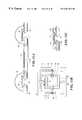
- FIG. 1shows a perspective illustration of a torsional micro-mirror system.
- Support posts 1are mounted to a base 2 .
- a mirror 3 and mirror support structure 4are provided between the posts and are suspended by torsional springs 5 .
- a cavity 6 formed in the base 2 below and around the mirror support structure 4is provided to facilitate the rotation of the mirror. The deeper the cavity 6 , the greater the rotation angle of the mirror. In some embodiments of the invention, the cavity extends entirely through the base so that the base does not limit the rotation at all.
- the mirror shown in FIG. 1is rectangular, the mirror support structure and mirror surface may be any practical shape including round, ovoid, or octagonal, and may be selected to reduce the mass of the mirror support structure, while still yielding a satisfactory mirror area.
- FIG. 2Ashows a plan view of one preferred embodiment
- FIG. 2Bshows the cross section of the system shown in FIG. 2A, taken along centerline 7
- the inventionconsists of a mirror surface 3 , parallel in this case with the surface of base 2 and suspended above an opening 6 in the base by two torsional springs 5 .
- the springs 5are collinear and aligned with the mirror support structure 4 centerline 7 , and are offset from the substrate and mirror surface by posts 1 .
- the mirror surface 3may be formed by vapor deposition of a metal such as Al onto mirror support structure 4 .
- Metallized regions 8 on the base surface, under the spring 5 and offset laterally from the centerline 7form one plate of the electrostatic drive capacitor, and the spring 5 serves as the other plate. Electrical contact to the drive capacitor plates is made by microfabricated conduction lines, and isolation between the conductors and the base is achieved by an oxide layer 13 formed on the surface of the substrate.
- the posts 1 offsetting the springs 5 from the substrate surfaceset the size of the
- a preferred embodiment of the inventionis designed to be operated at the resonance frequency of the device, which depends on the geometry and thickness of the mirror and the shape and material of the supports, as will be discussed later.
- necked down regions 9reduce the spring constant of the springs 5 and reduce the driving force required for actuation.
- the reduced spring constantalso reduces the resonant frequency.
- the extent of motion in response to a given drive voltageis determined by the stiffness of the springs 5 , including necked down regions 9 , and the size of the gap 10 between springs 5 and plates 8 , the area of the plates 8 , and the quality factor Q of the resonant structure.
- the maximum displacementis limited by the angle the torsional spring can twist through before the edge of the spring contacts the base.
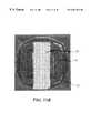
- a plan view scanning electron micrograph of a mirror system formed in this wayis shown in FIG. 3 .
- FIGS. 4A and Billustrate one spring design, in which it can be seen that electrostatic force pads 11 , 12 , placed on an oxide 13 upon base 2 (not behind the mirror), are connected to pads 14 and 15 .
- FIG. 4Bshows a cross sectional view along line 16
- FIG. 5shows a scanning electron micrograph of a spring system formed in this way. Spring 5 , (metallic in this embodiment), is connected to pad 17 .
- An electrostatic driving forcecan be applied between the spring 5 and the fixed force plate 12 by biasing pad 15 (in electrical contact with 12 through wire trace 18 ) with respect to pad 17 (in contact with spring 5 through trace 19 ), and similarly, a force can be applied between fixed force plate 11 and spring 5 by biasing pad 14 with respect to pad 17 .
- biasing the pads with a periodic potential at or near the resonant frequency of the systemwill excite resonant motion of the mirror.
- the resonant motionmay be excited by biasing only one plate and in such a case the other plate may be used for sensing the motion of the mirror by measuring the capacitance changes as the gap changes.
- an AC biasmay be applied between spring 5 and plate 11 at or near the resonant frequency to induce motion, and a DC bias voltage applied between plate 12 and spring 5 .
- the changes in capacitance between spring 5 and plate 12 owing to the motion of the spring 5may be sensed by monitoring the current at pad 12 .
- one or both of the springs 5may be biased and or sensed.
- the force padsare not behind the mirror, thus the mirror motion is not limited by the problem of the mirror contacting the force pad.
- the springitself may contact the base, which will ultimately limit the range of motion of the mirror; however, the spring and force pads may be designed to yield a much greater range of motion, as we will show in the various preferred embodiments.
- the fixed force plates 11 , 12may be designed so as to prevent electrical contact between the spring 5 and the fixed plates 11 , 12 , for example by coating the plates with a dielectric or by limiting the width of the plates so that the distance from the centerline to the plate edge is less than the product of one half the spring width and the cosine of the maximum deflection angle.
- a mirrormay be physically bonded to mirror support structure 4 (FIG. 2 ).
- the spring 5also serves as the mirror support structure, and extends across the cavity 6 .
- the mirroris bonded directly to this spring.
- These external mirrors 20could be made of materials that are not convenient to include in the fabrication process, or could be made of mirrors having optical power.
- the approach shown in FIG. 6has the additional and desirable feature that the cavity in the base wafer may be formed by etching only from the front side of the wafer.
- FIG. 7Another embodiment of the invention uses a different electrostatic capacitor design for the drive, and is shown in FIG. 7.
- a pair of electrodes 21is formed along the edges of the mirror parallel to the rotation axis.
- a second pair of electrodes 22is formed on the base along the edges of the cavity nearest the mirror electrode.
- the force resulting from an applied voltageis proportional to the capacitance between the electrodes, which is inversely proportional to the gap between them.
- no gapis required between the torsional springs 5 and the base 2 , so the fabrication of the posts may be eliminated if desired.
- the length of the freely rotating portion of the springs 5may be controlled by enlarging the width of the cavity 6 so as to increase the distance 23 between the mirror support structure 4 and the base 2 .
- the distance 23may differ from the distance 24 between electrodes 21 and 22 .
- a variation of the designinvolves magnetic actuation of the structure (FIGS. 8A though 8 D), again without restricting the freedom of motion of the mirror.
- magnetic material 25is applied to the mirror support structure (FIG. 8A) partially or totally covering the structure surface in order to give it a magnetic moment.
- the driving fieldis provided by an external electromagnet 26 which exerts a torque on the magnetic structure, causing the mirror support to rotate.
- the electromagnetmay be placed at a sufficient distance from the mirror to allow free rotation. However, if only limited motion is required, the magnetic coil may be placed closer to the mirror, thus reducing the coil current necessary to achieve actuation.
- the magnetic materialmay be patterned to improve the magnetic and mechanical performance of the device. Specifically (FIG. 8B) the material may be confined near the axis of rotation so as to minimize its moment of inertia and avoid lowering the resonant frequency, and may be shaped into one or several elongated structures 27 so that the preferred magnetic axis is perpendicular to the rotation axis.
- the magnetic materialmay either have a permanent magnetic moment or temporarily acquire a moment upon the establishment of an external magnetic field, in which case the torque is due to the shape anisotropy of the magnetic structure.
- the electrodeposited layer comprising the springsmay be chosen to be of a magnetic material, for example (but not necessarily) permalloy, in which case the magnetic structure may be formed in the same operation as the fabrication of the springs, or incorporated into the design of the springs themselves. Alternatively, two different materials may be used for the springs and magnetic structures, which may be formed in separate steps. Alternately, the magnetic material may be separately deposited or laminated onto the structure, in which case the magnetic material need not be formed by or even be compatible with standard fabrication processes, allowing the use of, for example, ceramic ferromagnets.
- Another approachcomprises patterning of a conduction coil 28 (FIG. 8C) onto the mirror support structure, which creates a magnetic moment when current is established. If multiple turns are used, a bridging structure 29 may be fabricated to connect the center of the coil to the electric leads. The magnetic moment established when current flows in the coil interacts with the field of a small permanent magnet 30 to rotate the mirror support structure to the desired angle.
- FIG. 8 DYet another approach to magnetic actuation uses a reluctance circuit approach (FIG. 8 D).
- One or more external electromagnets 31are mounted either slightly displaced above the mirror structure or at an angle to it.
- the magnetic material 32is pulled towards the center of the coil, forming part of the electromagnet core.
- additional magnetic material 33may be deposited on the base 2 for the attachment of the external coils 31 and used to define the shape of the applied magnetic field.
- the electromagnetmay be fabricated on the wafer using standard techniques.
- a fifth approach to magnetic actuationuses a permanent magnet attached to the mirror structure to provide a magnetic moment normal to the mirror surface. See FIG. 8 E.
- a magnetic field applied parallel to the mirror surface and orthogonal to the axis of rotationexerts a torque on the permanent magnet causing the mirror to rotate.
- the fieldcould be produced, for example, by a pair of electromagnet coils placed on either side of the mirror along an axis orthogonal to the rotation axis, with the coil axis parallel to the surface of the mirror.
- Yet another embodiment of the inventionsuspends the mirror about an axis of rotation 34 displaced from its centerline 7 , as shown in FIG. 9, allowing greater linear displacement on one side of the axis of rotation than the other.
- a large movable capacitor plate 35is arranged to push on the springs 5 .
- the large fixed plate 36is biased with respect to plate 35 , thereby generating a large force which is transferred to the springs.
- the force of plate 35may also be transferred directly to the mirror by an arm 37 as shown in FIG. 10A, which may or may not be attached to the mirror.
- the drive of the mechanical actuatormay be electrostatic, magnetic, or piezoelectric. An image of a scanning electron micrograph of such a device is shown in FIG. 10 B.
- one or both springsmay be split into two elements 99 along the axis of rotation 7 (FIG. 11) in order to provide additional electrical paths onto the mirror support assembly.
- rotational compliance of the springsmay be replaced by bending or twisting of the support posts 100 at the mirror support platform. This has the further advantage that the rotational motion of the mirror support platform can result from cantilevered bending of the springs.
- the springsmay be made as wide as desired to increase the electrostatic force. Applying a voltage between the springs and the capacitor plates on the fixed base, alternately on each side of the centerline 7 , causes the springs to bend and push down on the support platform.
- Video imagesrequire sweeping in two orthogonal directions, but the second sweep direction need not move faster than the frame rate, ranging from 30-180 Hz.
- two separate mirrorscould be used, rotating about orthogonal axes, or a single reflecting surface could be made to scan both directions.
- a single mirror that scans two orthogonal directionsis achieved either by mounting the current invention on a scanning platform, or modifying the design so the reflecting surface is supported within a gimballed frame, and made to scan in both directions.
- the actuating mechanism for the two directionscould be direct or indirect electric or magnetic force, or any combination thereof.
- a multi-axial micro-mirrormay be formed using the designs and processes described herein.
- the actuation mechanism for the two directionsis direct or indirect electric or magnetic force, or any combination thereof.
- FIG. 12illustrates one possible multi-axial design: a first pair of springs 38 is used for rotation of the mirror support structure 4 along one axis, and a second pair of springs 39 is used for rotation along a second axis which in this case is perpendicular to the first axis.
- the first pair 38joins the base 40 to a movable support frame 41 ; this support frame 41 is connected to the mirror support structure 4 by the second pair 39 .
- the deflection voltageis supplied to the pair 38 through bias applied to pads 42 and 43 , and through bias applied through pads 44 and 45 .
- the deflection voltage for pair 39is supplied through pair 38 by traces 46 and 47 .
- separate electrical contactsare to be provided for the inner mirror of a gimballed structure, they may be combined with the mechanical support of the outer mirror support frame, or may be run through separate structures bridging the gap between the inner and outer support structures, as shown in FIG. 13 .
- These separate structuresmay or may not contribute to the mechanical properties of the system.
- the structuresmay either be added as part of the packaging process, such as the addition of wire-bond wire jumpers 48 in FIG. 13A, or may be fabricated along with the rest of the structure.
- An example of integrally fabricated contact structures which minimally impact the mechanical propertiesis shown in FIG. 13 B.
- Soft serpentine springs 49bridge the gap, and connect through traces 50 to the inner springs 39 .
- the outer springs 38are separately connected to the drive pads 11 and 12 by traces 52 and 53 respectively. Multilayered spring supports may also be used to increase the number of separate electrical paths to the inner mirror.
- FIG. 13Cshows such a spring; an insulating layer 54 separates the upper conducting layer 55 from the lower conducting layer 56 . Each conducting layer connects to a separate pair of traces (not shown).
- the inner and outer support structuresmay have different damping characteristics.
- the line scanning structuremay be resonantly driven and benefit by low damping (high Q), while the frame scanning structure is driven linearly at low frequency and benefits from high damping for uniform motion.
- the devicecan be operated in a vacuum package to minimize the air damping of the fast mirror, with specific damping means provided for the slow scanning structure.
- a damping material 57may be applied to the slow moving structure or the springs (FIG. 14 A). This damping material may consist of a liquid, gel, or soft semi-solid surrounding the springs, with or without an enclosure to confine it.
- vacuum greasesuch as Dow Corning DC 976 or Apiezon N type, RTV silicone, or spin-on polymers used in the fabrication process such as polyimide or photoresist (for example Shipley AZ1308).
- vacuum greasesuch as Dow Corning DC 976 or Apiezon N type, RTV silicone, or spin-on polymers used in the fabrication process such as polyimide or photoresist (for example Shipley AZ1308).
- One embodimentis the application of a drop of DC 976 57 to the substrate so that it encloses the springs (FIG. 14 A).
- the damping material 98may instead be applied along the moving edge away from the spring (FIG. 14 B), so that it bridges the gap between the moving support element and the fixed base of the device.
- the damping materialmay be applied anywhere along the gap between the moving component and the fixed component, or between two components moving at different velocities, for example, the mirror platform and the gimballed outer frame of a biaxial embodiment.
- An alternativeis to coat the springs 38 with a high damping coating such as photoresist 58 (FIG. 14 C).
- Another alternativeis to enclose a high damping material within the springs, for example by making a multilayer structure incorporating high strength layers 59 surrounding high damping layers 60 . Damping may also be provided by mechanically attaching damping devices (dashpots) between the moving structure and the base.
- FIG. 15Ais a micrograph image of a biaxial scanning display device.
- the inner mirror support platform 4is the line scanner, driven by an electrostatic resonant drive.
- the oxidehas been removed from its surface and it has been coated with aluminum to form the mirror reflective surface.
- the electrical ground lead contactis made through the outer frame supports 38 and the drive voltage contacts are made by wire-bond wire jumpers 48 .
- the outer frameis the frame scanning direction and is driven magnetically to give a slow linear sweep and a fast retrace. Harmonic oscillations in the motion are damped by the application of approximately 0.005 microliters of DC 976 vacuum grease 57 to dampen the slow axis springs 38 .
- the magnetic momentis provided by magnetic foil 25 laminated to the back of the structure, covering half the area and placed orthogonal to the axis of rotation (FIG. 15 B). This device is then mounted on a small electromagnet and packaged in vacuum.
- the mirror support platformis approximately 1 mm x 1 mm and has a resonant frequency ranging from 7 to 15 kHz.
- the resonant frequency of the outer frameis 150 to 700 Hz.
- the outer frameis driven at 60 Hz.
- the deviceis packaged in vacuum above an electromagnetic coil, preferably in a T05 package containing optics.
- the mirror support structure 92is connected to the base 40 along one edge 94 by one or several metal cantilever springs 93 , allowing the mirror support structure to rotate out of the plane of the wafer.
- the stiffness of the support springs 93depends on the total aggregate width, but this width may be distributed among as many supports as desired (five in FIG. 16 ), each providing a separate electrical path onto the mirror support structure.
- Other devicesfor example a torsional MEMS mirror such as described herein, a CMOS circuit, for example the drive circuit, or both, may be fabricated on or grafted onto the platform 92 .
- the number of possible electrical contactsis limited only by the length of the edge 94 and the minimum practical width and separation of the springs 93 .
- This embodimentis an improvement to the mirror disclosed in the literature by Miller, in that the support springs are conducting and may provide multiple distinct electrical contacts to elements on the mirror support platform.
- the platform in the present inventionmay be formed of the original wafer, which may be a single crystal semiconductor, and may have a desired thickness up to the full thickness of the original wafer. Thus, it may comprise any desired CMOS circuit or device, which may be fabricated on the substrate prior to the release of the cantilevered platform.
- the motion of the platform 92may be used either to set the angle 95 between the platform 92 (and any devices carried upon it) and the base 40 (and any other devices attached to it), for example for the purpose of optical alignment, or to sweep the angle, for example for a display.
- the cantilevermay be moved into place mechanically, for example during the fabrication or packaging of the device, and locked into place, to fix the angle.
- magnetic materialmay be applied to the front, back, or both surfaces of the platform and a magnetic field may be applied to it during operation to rotate it to the desired angle.
- a DC magnetic field biasmay be applied to set the center angle of motion, and an AC field superimposed on it to sweep the angle. Either the AC or DC component may be zero.
- mechanical elementssuch as levers may be provided to set the angle during operation.
- Sensorsmay be added to the mirror to detect its position and the extent of the motion and provide feedback for the drive electronics.
- One sensor designconsists of capacitors similar to but separate from the drive pads, with detection of the current changing as a function of mirror position as previously described. If magnetic material is present on the moving structure, a magnetic sensor, for example a pickup coil, may be placed in close proximity to detect the mirror position. Optical sensing may also be utilized, as shown in FIG. 17.
- a light source 61provides a focused beam 62 which is reflected off the mirror 3 and detected by a detector 63 . As the mirror rotates, the intensity of light incident on the detector 63 changes and can be correlated with mirror angle.
- the angle of incidence 64can be chosen so the sensing light does not interfere with the display illumination, or an infrared source may be used.
- the detectionmay be made from the back of the mirror structure by reflecting the light off the back of the mirror support structure 4 .
- the mirror positionmay be determined by sensing the light incident on it for display illumination. Detection may also be made by allowing invisible radiation such as infrared light to pass through a specifically designed mirror surface coating to a detector mounted on the back of or underneath the device.
- the forceis proportional to the square of the applied voltage and inversely proportional to the square of the gap 12 (FIG. 2) between the drive capacitor plates.
- Making the gap smaller or the spring widerreduces the maximum angle of rotation but increases the applied torque, while making the gap 12 larger or the support narrower allows greater motion but reduces the torque resulting from a given applied voltage.
- At the maximum displacementat least some portion of the spring 5 touches the base 2 .
- the present inventionis designed so that the mirror itself is free to rotate to any degree within the elastic limits of the springs, and the displacement is limited by the rotation of the springs in relation to the base. For a fixed gap height g, if at any given point z along the length of the spring its width is w(z), then the maximum rotation allowed at that point is approximately
- the angle of rotationvaries along the length of the spring, from approximately zero at the connection to the support post to the maximum at the mirror support structure, and the spring shape can be designed to take advantage of this, for example by making the spring wider near the fixed end and narrower at the mirror support structure, allowing a greater angle of rotation while still allowing for a large plate area and thus allowing for application of a larger torque than would be obtained in a spring of uniform cross section.
- FIG. 18Several possible spring designs are shown in FIG. 18 .
- the stiffness of each designcan be calculated from standard mechanical expressions, for example as found in Mark's Handbook of Mechanical Engineering. T. Baumeister, editor in chief, Mark's Standard Handbook for Mechanical Engineers, 8th ed., McGraw-Hill Book Company, New York, 1978, Section 5.
- K tG 3.5 ⁇ ⁇ l ⁇ ⁇ ( b 3 ⁇ h 3 b 2 + h 2 )
- K tG 3.5 ⁇ ⁇ l i ⁇ ⁇ ( b i 3 ⁇ h 3 b i 2 + h 2 ) ,
- ⁇is the density of the mirror support structure
- Lis its length
- Wis its width (parallel to the axis of rotation)
- tits thickness.
- FIG. 18 Aillustrates a micro-mirror with tapered supports.
- FIG. 20Another design is shown in FIG. 20, in which the spring 5 has two necked down regions 67 , 68 , which facilitate a high rotation angle.
- the necked down regionsare separated by a wider region 69 which comprises the moving force plate 70 section of spring 5 .
- the mirror support structure 4can continue to rotate through an additional angle which is limited by the elastic limits of section 68 of spring 5 .
- the total rotation ⁇is given by:
- ⁇⁇ w 68 /w 67 .
- FIG. 21shows the fabrication process.
- a polished wafer 71preferably Si, is first coated on both sides with a material 72 on the front and 73 on the back that is resistant to etches of the wafer material.
- this materialmay be silicon nitride, silicon dioxide, or other films known in the art.
- the wafermay for example be oxidized to form a surface layer of silicon dioxide 72 , 73 on both sides of the wafer, or the wafer may be coated by chemical vapor deposition, or by other means.
- the wafer 71 and coatings 72 , 73are then patterned on both sides with registered alignment marks and etched to define the marks in the crystal. These marks, formed on both sides of the wafer, permit registration of features on the front and back (registration marks are not shown in FIG. 21 ).
- Metal filmsfor example of chromium, gold, and titanium/tungsten alloy, are deposited on the front coated surface 72 , and are patterned and etched to form pads 74 that provide the electrical contacts and anchors for the mechanical structures.
- the coating 73is patterned and etched to act as a mask for wafer etching.
- the back of the waferis then etched to form a membrane with surface 75 having thickness in the range of 20 ⁇ m to 200 ⁇ m. A typical thickness is 60 ⁇ m.
- the coating 72 on the front surfaceis then patterned and etched to form groove openings 76 in the coating which will serve later in the process as an etch mask for the separation of the mirror support structures 4 from the base 2 .
- the initial coatingsmay also include or serve as the final mirror surface.
- a release layer 77 of photoresist or other materialis applied to the front surface and patterned with holes 78 to expose the metal anchors 74 .
- thin (.05 ⁇ m to .5 ⁇ m) layers of a metal or sequence of metals such as chromium, gold and titanium/tungsten alloy 79are deposited on the front surface.
- Photoresistis then applied and patterned to form a mask 80 for the electrodeposited structures.
- a metal layer 81which may be nickel, is deposited by electroplating on to the exposed regions 82 of metal layers 74 and 79 .
- the thickness of metal layer 81is in the range of 0.5 ⁇ m to 10 ⁇ m; layer 81 constitutes the spring 5 in the plan views described earlier.
- the mask 80 and release layer 77are removed by dissolving the layers in solvents or preferential etches. This process also removes sections of intermediate metal layers 83 (of metal layer 79 ) that are not reinforced by the electroplating.
- the waferis diced, and the mirror support structure 4 is separated from the surrounding base 2 by etching both from the front, through the grooves 76 defined in the etch masks 72 and 73 , and from the back by etching surface 75 , resulting in the formation of cavity 6 surrounding the mirror support structure 4 .
- the mirror support structure 4is thus joined to the base solely by the metal torsional springs 5 .
- the final thickness of the mirror support structure 4depends on the duration of the two etch steps and can be selected to yield structures with thickness in the range of 10 to 200 ⁇ m or more (as large as the wafer thickness if needed). Typical final support structure thickness is 30 ⁇ m.
- the final stepcomprises addition of a mirror, either by providing a metal or dielectric coating 84 (FIG. 22A) of the mirror support structure through a mask (for example with evaporated or sputtered aluminum with thickness in the range of 500 to 2500 angstrom), or by bonding a finished mirror to the support structure.
- FIG. 22Bshows a mirror bonded to the mirror support structure, comprising an adhesive or other attachment layer 85 , a glass or other substance 86 as is used in the art of mirror formation to support a reflecting layer, and a flat mirror (reflecting) layer 87 .
- This inventionadditionally comprises the capability to use a mirror comprising a curved surface formed in material 86 and coated with a reflecting layer 88 , as shown in FIG. 22 C.
- This surface on material 86may be either convex or concave, or aspherical.
- the layers 87 or 88may comprise a binary optical element of a diffractive or refractive nature, or a holographic element.
- any of the coatings used in the fabrication processmay have a high degree of internal stress. If the mirror support structure is sufficiently thin, this stress could induce curvature in the structure. This curvature may be useful, for example for shaping the optical surface, or may be undesirable. In the latter case, if it is not possible or desirable to remove the stressed film, additional layers 89 of equal stress may be deposited on the back face of the structure to compensate for the stress and restore the surface flatness (FIG. 22 D). Alternately, the compensating layer may be applied to the front of the support structure, under the mirror, in which case the compensating layer stress would be equal and opposite to the stress already present. If the reflectance of the compensation material is sufficient (e.g. if chromium is used), it may serve as the reflective surface as well.
- the mirror thicknessis determined by the duration of the etch used to remove the excess material from the back. The choice of thickness results from a tradeoff between mechanical stiffness, moment of inertia, and thermal conductivity. Thicker mirrors are stiffer, and so deform less in use, but the additional mass results in a higher moment of inertia which lowers the resonant frequency.
- backside patterning of the mirror support structureto the fabrication process as shown in FIG. 23, an engineered mirror support structure can be made, so as to yield a support which is stiff yet low in mass. For example, by adding a patterned mask 90 to the back etching, support ribs could be fabricated 91 on the back of the mirror, perpendicular to the rotation axis, adding stiffness but minimal weight.
- a corrugated, honeycomb, or other structuremay be formed by etching a pattern of wells into the back of the mirror support structure.
- Another method that can be applied when the substrate is a single crystal (such as Si)is to pattern the back surface with an array of square openings aligned to the crystal axis, followed by etching in a selective etch (such as potassium hydroxide etching of Si) which etches ⁇ 111 ⁇ planes much more slowly than other planes of the crystal.
- a selective etchsuch as potassium hydroxide etching of Si
- Structures having a magnetic moment, for use in magnetic actuationmay be electroplated in the same manner as the springs. If the material used for the springs is magnetic, they may be deposited at the same time as the springs. If two different materials are to be used, the magnetic structures may be electroplated in a separate step using a similar processing sequence to that described above.
- a third option for applying magnetic material to the structureconsists of attaching a pre-formed magnetic element to the completed device by means of an adhesive such as cyanoacrylate adhesive or Crystal Bond wax.
Landscapes
- Physics & Mathematics (AREA)
- General Physics & Mathematics (AREA)
- Optics & Photonics (AREA)
- Electromagnetism (AREA)
- Micromachines (AREA)
- Mechanical Light Control Or Optical Switches (AREA)
- Mechanical Optical Scanning Systems (AREA)
Abstract
Description


Claims (60)
Priority Applications (3)
| Application Number | Priority Date | Filing Date | Title |
|---|---|---|---|
| US09/138,367US6201629B1 (en) | 1997-08-27 | 1998-08-26 | Torsional micro-mechanical mirror system |
| US09/753,512US6353492B2 (en) | 1997-08-27 | 2001-01-03 | Method of fabrication of a torsional micro-mechanical mirror system |
| US09/753,510US6538799B2 (en) | 1997-08-27 | 2001-01-03 | Magnetically actuated torsional micro-mechanical mirror system |
Applications Claiming Priority (2)
| Application Number | Priority Date | Filing Date | Title |
|---|---|---|---|
| US5770097P | 1997-08-27 | 1997-08-27 | |
| US09/138,367US6201629B1 (en) | 1997-08-27 | 1998-08-26 | Torsional micro-mechanical mirror system |
Related Child Applications (2)
| Application Number | Title | Priority Date | Filing Date |
|---|---|---|---|
| US09/753,510DivisionUS6538799B2 (en) | 1997-08-27 | 2001-01-03 | Magnetically actuated torsional micro-mechanical mirror system |
| US09/753,512DivisionUS6353492B2 (en) | 1997-08-27 | 2001-01-03 | Method of fabrication of a torsional micro-mechanical mirror system |
Publications (1)
| Publication Number | Publication Date |
|---|---|
| US6201629B1true US6201629B1 (en) | 2001-03-13 |
Family
ID=26736800
Family Applications (3)
| Application Number | Title | Priority Date | Filing Date |
|---|---|---|---|
| US09/138,367Expired - LifetimeUS6201629B1 (en) | 1997-08-27 | 1998-08-26 | Torsional micro-mechanical mirror system |
| US09/753,510Expired - LifetimeUS6538799B2 (en) | 1997-08-27 | 2001-01-03 | Magnetically actuated torsional micro-mechanical mirror system |
| US09/753,512Expired - LifetimeUS6353492B2 (en) | 1997-08-27 | 2001-01-03 | Method of fabrication of a torsional micro-mechanical mirror system |
Family Applications After (2)
| Application Number | Title | Priority Date | Filing Date |
|---|---|---|---|
| US09/753,510Expired - LifetimeUS6538799B2 (en) | 1997-08-27 | 2001-01-03 | Magnetically actuated torsional micro-mechanical mirror system |
| US09/753,512Expired - LifetimeUS6353492B2 (en) | 1997-08-27 | 2001-01-03 | Method of fabrication of a torsional micro-mechanical mirror system |
Country Status (1)
| Country | Link |
|---|---|
| US (3) | US6201629B1 (en) |
Cited By (228)
| Publication number | Priority date | Publication date | Assignee | Title |
|---|---|---|---|---|
| WO2001095006A1 (en)* | 2000-06-06 | 2001-12-13 | Iolon, Inc. | Damped micromechanical device and method for making same |
| US20020005976A1 (en)* | 2000-03-24 | 2002-01-17 | Behrang Behin | Multi-layer, self-aligned vertical combdrive electrostatic actuators and fabrication methods |
| US6359718B1 (en)* | 2001-02-01 | 2002-03-19 | Walsin Lihwa Corporation | Actuating mechanism for rotating micro-mirror |
| US6379510B1 (en)* | 2000-11-16 | 2002-04-30 | Jonathan S. Kane | Method of making a low voltage micro-mirror array light beam switch |
| US20020085594A1 (en)* | 2000-10-30 | 2002-07-04 | Bardia Pezeshki | Tunable controlled laser array |
| US20020090011A1 (en)* | 2000-10-30 | 2002-07-11 | Bardia Pezeshki | Laser thermal tuning |
| US20020105653A1 (en)* | 2001-01-16 | 2002-08-08 | Bardia Pezeshki | Tunable optical device using a scanning MEMS mirror |
| US6433390B1 (en)* | 1999-07-26 | 2002-08-13 | Sony Corporation | Bonded substrate structures and method for fabricating bonded substrate structures |
| US6441360B1 (en)* | 1999-11-10 | 2002-08-27 | Lucent Technologies, Inc. | MEMS optical isolators |
| US6445362B1 (en)* | 1999-08-05 | 2002-09-03 | Microvision, Inc. | Scanned display with variation compensation |
| WO2002086602A1 (en)* | 2001-04-17 | 2002-10-31 | M2N, Inc. | Micro-actuator and micro-device using the same |
| GB2375185A (en)* | 2001-05-04 | 2002-11-06 | Kymata Ltd | Thick wafer for MEMS fabrication |
| WO2002088804A1 (en)* | 2001-04-25 | 2002-11-07 | Umachines, Inc. | Silicon micromachined optical device |
| US20020164113A1 (en)* | 2001-03-05 | 2002-11-07 | The Microoptical Corporation | Micro-electromechanical optical switch assembly for optical data networks |
| EP1258769A1 (en)* | 2001-05-08 | 2002-11-20 | Samsung Electronics Co., Ltd. | Optical module and method for manufacturing the same |
| US6491404B2 (en) | 2001-02-23 | 2002-12-10 | Jds Uniphase Corporation | Microelectromechanical apparatus with tiltable bodies including variable tilt-stop engaging portions and methods of operation and fabrication therefor |
| US6496612B1 (en)* | 1999-09-23 | 2002-12-17 | Arizona State University | Electronically latching micro-magnetic switches and method of operating same |
| US20030002195A1 (en)* | 2001-05-31 | 2003-01-02 | Stmicroelectronics S.R.L | Tiltable device, in particular hard disk actuator device, with roll and pitch angle active control |
| US6504641B2 (en)* | 2000-12-01 | 2003-01-07 | Agere Systems Inc. | Driver and method of operating a micro-electromechanical system device |
| US20030016428A1 (en)* | 2001-07-11 | 2003-01-23 | Takahisa Kato | Light deflector, method of manufacturing light deflector, optical device using light deflector, and torsion oscillating member |
| US20030030919A1 (en)* | 2001-08-08 | 2003-02-13 | Bardia Pezeshki | Method and system for selecting an output of a VCSEL array |
| US20030039021A1 (en)* | 2001-08-02 | 2003-02-27 | Dinh Ton | MEMS mirror |
| WO2002091025A3 (en)* | 2001-05-04 | 2003-02-27 | L3 Optics Inc | Method and apparatus for detecting and latching the position of a mems moving member |
| US20030043373A1 (en)* | 2001-08-31 | 2003-03-06 | Respironics, Inc. | Microspectrometer gas analyzer |
| US20030048390A1 (en)* | 2001-08-17 | 2003-03-13 | Cae Inc. | Video projector and optical light valve therefor |
| WO2002073285A3 (en)* | 2001-03-12 | 2003-03-13 | Axsun Tech Inc | Mems membrane with integral mirror/lens |
| US6535318B1 (en)* | 1999-11-12 | 2003-03-18 | Jds Uniphase Corporation | Integrated optoelectronic devices having pop-up mirrors therein and methods of forming and operating same |
| US20030053156A1 (en)* | 2001-08-20 | 2003-03-20 | Yukito Satoh | Optical scanning device and image forming apparatus using the same |
| US20030057350A1 (en)* | 2001-09-27 | 2003-03-27 | Miller Samuel Lee | Large tilt angle MEM platform |
| US20030076664A1 (en)* | 2000-04-05 | 2003-04-24 | Milasys Gbr | Micro-functional unit |
| US6556741B1 (en) | 2000-10-25 | 2003-04-29 | Omm, Inc. | MEMS optical switch with torsional hinge and method of fabrication thereof |
| US6567574B1 (en) | 2000-10-06 | 2003-05-20 | Omm, Inc. | Modular three-dimensional optical switch |
| US6577431B2 (en)* | 2001-06-15 | 2003-06-10 | Industrial Technology Research Institute | System of angular displacement control for micro-mirrors |
| US20030123788A1 (en)* | 2002-01-03 | 2003-07-03 | Miller Samuel Lee | Off axis optical signal redirection architectures |
| US20030123128A1 (en)* | 2001-12-19 | 2003-07-03 | Lg Electronics Inc. | Micromirror in cross-connect switch for optical communication system and method for fabricating the same |
| US6593677B2 (en) | 2000-03-24 | 2003-07-15 | Onix Microsystems, Inc. | Biased rotatable combdrive devices and methods |
| US6608711B2 (en)* | 2000-03-03 | 2003-08-19 | Axsun Technologies, Inc. | Silicon on insulator optical membrane structure for fabry-perot MOEMS filter |
| US20030176007A1 (en)* | 2000-06-13 | 2003-09-18 | Andreas Bertz | Microstructure and method for the production thereof |
| US20030174382A1 (en)* | 2001-12-26 | 2003-09-18 | Jean-Louis Massieu | Frame grabbing with laser scanner with sweeping by silicon planar electrostatics actuator |
| US6629461B2 (en) | 2000-03-24 | 2003-10-07 | Onix Microsystems, Inc. | Biased rotatable combdrive actuator methods |
| WO2002097478A3 (en)* | 2001-05-30 | 2003-10-09 | Fiberyard Inc | Optical beam steering device |
| US6632373B1 (en)* | 2000-09-28 | 2003-10-14 | Xerox Corporation | Method for an optical switch on a substrate |
| US6632374B1 (en) | 2000-09-28 | 2003-10-14 | Xerox Corporation | Method for an optical switch on a silicon on insulator substrate |
| WO2003085442A1 (en)* | 2002-04-11 | 2003-10-16 | Memscap | Component comprising at least one cell including a mems structure |
| US6640023B2 (en) | 2001-09-27 | 2003-10-28 | Memx, Inc. | Single chip optical cross connect |
| US6646215B1 (en) | 2001-06-29 | 2003-11-11 | Teravicin Technologies, Inc. | Device adapted to pull a cantilever away from a contact structure |
| US6657764B1 (en)* | 1999-03-18 | 2003-12-02 | The Trustees Of Boston University | Very large angle integrated optical scanner made with an array of piezoelectric monomorphs |
| WO2003089957A3 (en)* | 2002-04-17 | 2003-12-04 | M2N Inc | Micro piezoelectric actuator and method for fabricating same |
| US20030223679A1 (en)* | 2002-05-28 | 2003-12-04 | Mohiuddin Mala | Piano MEMs micromirror |
| US20030227700A1 (en)* | 2002-06-11 | 2003-12-11 | Fujitsu Limited | Micro mirror unit and method of making the same |
| US6666561B1 (en) | 2002-10-28 | 2003-12-23 | Hewlett-Packard Development Company, L.P. | Continuously variable analog micro-mirror device |
| US6670809B1 (en)* | 2000-08-18 | 2003-12-30 | The United States Of America As Represented By The Secretary Of The Army | Magnetic sensor with modulating flux concentrator having minimized air resistance for 1/f noise reduction |
| US20040008400A1 (en)* | 2001-12-05 | 2004-01-15 | Jds Uniphase Corporation | Articulated MEMS electrostatic rotary actuator |
| US6681063B1 (en)* | 2000-11-16 | 2004-01-20 | Computer Optics Inc | Low voltage micro-mirror array light beam switch |
| US20040013431A1 (en)* | 2002-04-01 | 2004-01-22 | Ed Vail | Laser and laser signal combiner |
| US20040017625A1 (en)* | 2001-06-02 | 2004-01-29 | Van Drieenhuizen Bert P. | Bulk silicon mirrors with hinges underneath |
| US20040017599A1 (en)* | 2002-07-29 | 2004-01-29 | Xiaofeng Yang | Micro-mirror with rotor structure |
| US6687132B2 (en)* | 2001-02-05 | 2004-02-03 | Texas Instruments Incorporated | Conductive member grid array interface for mirror array drive apparatus |
| USRE38437E1 (en)* | 1998-12-01 | 2004-02-24 | Xerox Corporation | Method and apparatus for an integrated laser beam scanner using a carrier substrate |
| US6707355B1 (en) | 2001-06-29 | 2004-03-16 | Teravicta Technologies, Inc. | Gradually-actuating micromechanical device |
| US6711317B2 (en)* | 2001-01-25 | 2004-03-23 | Lucent Technologies Inc. | Resiliently packaged MEMs device and method for making same |
| US6709886B2 (en) | 2000-04-25 | 2004-03-23 | Umachines, Inc. | Method of fabricating micromachined devices |
| US20040084208A1 (en)* | 2002-10-30 | 2004-05-06 | Ives Thomas W. | Article and method for reducing external excitation of MEMS devices |
| US20040109222A1 (en)* | 2002-04-30 | 2004-06-10 | Nguyen Clark T.-C. | Low-voltage electromechanical device including a tiltable microplatform, method of tilting same, array of such devices and method of setting dimple-to-substrate spacing |
| US6754243B2 (en) | 2000-08-09 | 2004-06-22 | Jds Uniphase Corporation | Tunable distributed feedback laser |
| US6757093B2 (en) | 2001-05-21 | 2004-06-29 | Jds Uniphase Corporation | MEMS reflectors having tail portions that extend inside a recess and head portions that extend outside the recess and methods of forming same |
| US6758983B2 (en) | 2000-05-31 | 2004-07-06 | The Regents Of The University Of California | Staggered torsional electrostatic combdrive and method of forming same |
| US6760145B1 (en)* | 2003-01-23 | 2004-07-06 | Corning Incorporated | Actuator for dual-axis rotation micromirror |
| US20040130766A1 (en)* | 2002-11-08 | 2004-07-08 | Dewa Andrew Steven | Multilayered oscillating functional surface |
| US6771855B2 (en) | 2000-10-30 | 2004-08-03 | Santur Corporation | Laser and fiber coupling control |
| US20040155558A1 (en)* | 2002-04-08 | 2004-08-12 | University Of North Carolina At Charlotte | Tunable vibratory actuator |
| US20040160687A1 (en)* | 2001-06-02 | 2004-08-19 | Van Drieenhuizen Bert P. | High fill-factor bulk silicon mirrors |
| US6781734B2 (en) | 2001-03-30 | 2004-08-24 | Santur Corporation | Modulator alignment for laser |
| KR100447214B1 (en)* | 2002-02-08 | 2004-09-04 | 엘지전자 주식회사 | Micro mirror |
| US6787438B1 (en) | 2001-10-16 | 2004-09-07 | Teravieta Technologies, Inc. | Device having one or more contact structures interposed between a pair of electrodes |
| US20040179281A1 (en)* | 2003-03-12 | 2004-09-16 | Reboa Paul F. | Micro-mirror device including dielectrophoretic liquid |
| US20040178273A1 (en)* | 2003-03-13 | 2004-09-16 | Wood Frederick F. | Inertial drive scanning arrangement and method |
| US6795225B2 (en)* | 2001-07-04 | 2004-09-21 | Fujitsu Limited | Micromirror unit with torsion connector having nonconstant width |
| US20040184124A1 (en)* | 2002-11-13 | 2004-09-23 | Olympus Corporation | Optical deflection device |
| KR100451409B1 (en)* | 2002-10-15 | 2004-10-06 | 한국전자통신연구원 | Micro-optical switch and method for manufacturing the same |
| US20040207893A1 (en)* | 2002-03-14 | 2004-10-21 | Miller Samuel Lee | Channel processing unit for WDM network |
| US20040211655A1 (en)* | 1999-03-09 | 2004-10-28 | Behrang Behin | Method for directing an optical beam and a method for manufacturing an apparatus for directing an optical beam |
| US20040212865A1 (en)* | 2003-04-22 | 2004-10-28 | Motorola, Inc. | Optical reflecting device |
| US20040212907A1 (en)* | 2003-04-24 | 2004-10-28 | Mohiuddin Mala | Micro-electro-mechanical-system two dimensional mirror with articulated suspension structures for high fill factor arrays |
| US6813300B2 (en) | 2001-03-30 | 2004-11-02 | Santur Corporation | Alignment of an on chip modulator |
| WO2004094301A1 (en)* | 2003-04-24 | 2004-11-04 | Metconnex Canada Inc. | A micro-electro-mechanical-system two dimensional mirror with articulated suspension structures for high fill factor arrays |
| US6816529B2 (en) | 2001-03-30 | 2004-11-09 | Santur Corporation | High speed modulation of arrayed lasers |
| US20040223685A1 (en)* | 1996-07-30 | 2004-11-11 | Heanue John F. | Optical microdevice with rotatable microactuator |
| US20040246306A1 (en)* | 2000-02-03 | 2004-12-09 | Scott Adams | Electrostatic actuator for microelectromechanical systems and methods of fabrication |
| US6831772B2 (en) | 2002-02-01 | 2004-12-14 | Analog Devices, Inc. | Optical mirror module |
| WO2005006052A1 (en)* | 2003-07-14 | 2005-01-20 | Koninklijke Philips Electronics N.V. | Laser beam scanner |
| US20050018329A1 (en)* | 2002-01-24 | 2005-01-27 | Pesik Joseph T. | Silicon wafer based macroscopic mirror for wide angle scanning applications |
| US20050047010A1 (en)* | 2001-08-16 | 2005-03-03 | Nobuyuki Ishiwata | Thin film electromagnet and switching device comprising it |
| US6865195B2 (en)* | 2000-08-04 | 2005-03-08 | Avanex Corporation | Edge-emitting semiconductor tunable laser |
| US6888656B2 (en)* | 2000-11-20 | 2005-05-03 | Olympus Corporation | Optical deflector |
| US20050094401A1 (en)* | 2003-11-04 | 2005-05-05 | Simon Magarill | Side reflector for illumination using light emitting diode |
| US20050091975A1 (en)* | 2002-01-28 | 2005-05-05 | Technology Innovations, Llc | Microactivation using fiber optic and wireless means |
| US20050099671A1 (en)* | 2003-01-12 | 2005-05-12 | Olympus Corporation | Optical deflector array |
| US6906846B2 (en) | 2002-08-14 | 2005-06-14 | Triquint Technology Holding Co. | Micro-electro-mechanical system device and method of making same |
| US20050134811A1 (en)* | 2003-12-23 | 2005-06-23 | Simon Magarill | Combined light source for projection display |
| US6922278B2 (en) | 2001-03-30 | 2005-07-26 | Santur Corporation | Switched laser array modulation with integral electroabsorption modulator |
| US20050170557A1 (en)* | 2000-12-07 | 2005-08-04 | Patel Satyadev R. | Methods for depositing, releasing and packaging micro-electromechanical devices on wafer substrates |
| US20050174775A1 (en)* | 2004-02-11 | 2005-08-11 | 3M Innovative Properties Company | Light-collecting illumination system |
| US20050174768A1 (en)* | 2004-02-11 | 2005-08-11 | 3M Innovative Properties Company | Illumination system |
| US20050174771A1 (en)* | 2004-02-11 | 2005-08-11 | 3M Innovative Properties Company | Reshaping light source modules and illumination systems using the same |
| US20050185239A1 (en)* | 2002-11-08 | 2005-08-25 | Orcutt John W. | Multilayered oscillating device with spine support |
| US20050221529A1 (en)* | 2001-12-06 | 2005-10-06 | Microfabrica Inc. | Complex microdevices and apparatus and methods for fabricating such devices |
| US20050225822A1 (en)* | 2004-03-31 | 2005-10-13 | Canon Kabushiki Kaisha | Optical deflector having neutral surface of bending in movable member in different plane from neutral surface of bending in elastic support member |
| US20050243446A1 (en)* | 2004-04-30 | 2005-11-03 | Symbol Technologies, Inc. | Piezoelectric actuated scanning mirror |
| US6963679B1 (en)* | 2000-05-24 | 2005-11-08 | Active Optical Networks, Inc. | Micro-opto-electro-mechanical switching system |
| US20050254019A1 (en)* | 2004-05-14 | 2005-11-17 | 3M Innovative Properties Company | Illumination system with non-radially symmetrical aperture |
| US20060039140A1 (en)* | 2004-08-23 | 2006-02-23 | Simon Magarill | Multiple channel illumination system |
| US20060070379A1 (en)* | 2000-10-31 | 2006-04-06 | Microsoft Corporation | Microelectrical mechanical structure (MEMS) optical modulator and optical display system |
| US20060070451A1 (en)* | 2004-09-24 | 2006-04-06 | University Of Louisville Research Foundation, Inc. | MEMS capacitive cantilever strain sensor, devices, and formation methods |
| US20060076417A1 (en)* | 2004-08-30 | 2006-04-13 | Jean-Louis Massieu | Apparatus for diagonal progressive scanning video and method of improving aiming visibility, reducing tilt dependence and improving read range |
| WO2006063577A1 (en)* | 2004-12-16 | 2006-06-22 | Fraunhofer-Gesellschaft zur Förderung der angewandten Forschung e.V. | Method and projector for image projection |
| US7098871B1 (en)* | 1998-08-05 | 2006-08-29 | Microvision, Inc. | Optical scanning system with correction |
| US20060222312A1 (en)* | 2005-02-16 | 2006-10-05 | Mohiuddin Mala | Articulated MEMs structures |
| US7159397B1 (en)* | 2005-06-07 | 2007-01-09 | Sandia Corporation | Tensile-stressed microelectromechanical apparatus and tiltable micromirrors formed therefrom |
| US20070047113A1 (en)* | 2001-06-02 | 2007-03-01 | Capella Photonics, Inc. | High fill-factor bulk silicon mirrors with reduced effect of mirror edge diffraction |
| US7190509B2 (en) | 2001-11-07 | 2007-03-13 | Trex Enterprises Corp. | Optically addressed MEMS |
| US7190854B1 (en) | 2000-05-24 | 2007-03-13 | Active Optical Networks, Inc. | Methods for forming an array of MEMS optical elements |
| CN1310057C (en)* | 2002-06-28 | 2007-04-11 | 索尼公司 | Heat-driven micro reflecting-mirror and electronic apparatus |
| US20070164221A1 (en)* | 2001-08-31 | 2007-07-19 | Russell James T | Microspectrometer gas analyzer |
| US20070176719A1 (en)* | 2000-04-07 | 2007-08-02 | Microsoft Corporation | Magnetically Actuated Microelectromechanical Systems Actuator |
| CN100365466C (en)* | 2005-01-12 | 2008-01-30 | 夏普株式会社 | light scanning device |
| US20080025359A1 (en)* | 2006-07-26 | 2008-01-31 | Bardia Pezeshki | Modulated semiconductor dfb laser array with a mems-based rf switch |
| US20080062161A1 (en)* | 1999-08-05 | 2008-03-13 | Microvision, Inc. | Apparatuses and methods for utilizing non-ideal light sources |
| EP1542059A4 (en)* | 2002-08-14 | 2008-07-30 | Fujitsu Ltd | TORSION BAR MICRO TILTING DEVICE |
| US20080192327A1 (en)* | 2006-12-29 | 2008-08-14 | Abu-Ageel Nayef M | Method and system for speckle reduction using an active device |
| US20090015956A1 (en)* | 2007-07-10 | 2009-01-15 | Motorola, Inc. | Method and Apparatus for Coupling a Microelectromechanical System Scanner Mirror to a Frame |
| WO2009107922A1 (en)* | 2008-02-25 | 2009-09-03 | Samsung Electronics Co, . Ltd. | Micro electro-mechanical system mirror and scanning actuator employing the same |
| US20090321857A1 (en)* | 2008-06-25 | 2009-12-31 | Honeywell International Inc. | Systems and methods for reduced stress anchors |
| US20100147076A1 (en)* | 2006-12-18 | 2010-06-17 | Diamond Brett M | Proof-mass with supporting structure on integrated circuit-MEMS platform and method of fabricating the same |
| US7872394B1 (en) | 2001-12-13 | 2011-01-18 | Joseph E Ford | MEMS device with two axes comb drive actuators |
| CN101495904B (en)* | 2006-12-05 | 2011-04-20 | 松下电器产业株式会社 | actuator |
| US20110148554A1 (en)* | 2008-08-22 | 2011-06-23 | Korea Advanced Institute Of Science And Technology | Electromagnetic multi-axis actuator |
| JP2011123481A (en)* | 2009-10-29 | 2011-06-23 | Btendo Ltd | Method and device for monitoring movement of mirror in mems device |
| WO2012027410A1 (en)* | 2010-08-23 | 2012-03-01 | Lighttime, Llc | Ladar using mems scanning |
| US8189263B1 (en) | 2011-04-01 | 2012-05-29 | Google Inc. | Image waveguide with mirror arrays |
| US8294994B1 (en) | 2011-08-12 | 2012-10-23 | Google Inc. | Image waveguide having non-parallel surfaces |
| CN103048783A (en)* | 2012-12-21 | 2013-04-17 | 无锡微奥科技有限公司 | Thermally driven MEMS (Micro-Electro-Mechanical System) micromirror |
| US8467133B2 (en) | 2010-02-28 | 2013-06-18 | Osterhout Group, Inc. | See-through display with an optical assembly including a wedge-shaped illumination system |
| US8472119B1 (en) | 2011-08-12 | 2013-06-25 | Google Inc. | Image waveguide having a bend |
| US8471967B2 (en) | 2011-07-15 | 2013-06-25 | Google Inc. | Eyepiece for near-to-eye display with multi-reflectors |
| US8472120B2 (en) | 2010-02-28 | 2013-06-25 | Osterhout Group, Inc. | See-through near-eye display glasses with a small scale image source |
| US8477425B2 (en) | 2010-02-28 | 2013-07-02 | Osterhout Group, Inc. | See-through near-eye display glasses including a partially reflective, partially transmitting optical element |
| US8482859B2 (en) | 2010-02-28 | 2013-07-09 | Osterhout Group, Inc. | See-through near-eye display glasses wherein image light is transmitted to and reflected from an optically flat film |
| US8488246B2 (en) | 2010-02-28 | 2013-07-16 | Osterhout Group, Inc. | See-through near-eye display glasses including a curved polarizing film in the image source, a partially reflective, partially transmitting optical element and an optically flat film |
| US8503087B1 (en) | 2010-11-02 | 2013-08-06 | Google Inc. | Structured optical surface |
| US8508851B2 (en) | 2011-07-20 | 2013-08-13 | Google Inc. | Compact see-through display system |
| US8576143B1 (en) | 2010-12-20 | 2013-11-05 | Google Inc. | Head mounted display with deformation sensors |
| US8582209B1 (en) | 2010-11-03 | 2013-11-12 | Google Inc. | Curved near-to-eye display |
| US8636911B2 (en)* | 2010-10-07 | 2014-01-28 | Magic Technologies, Inc. | Process for MEMS scanning mirror with mass remove from mirror backside |
| US8666212B1 (en) | 2011-04-28 | 2014-03-04 | Google Inc. | Head mounted display using a fused fiber bundle |
| US8670000B2 (en) | 2011-09-12 | 2014-03-11 | Google Inc. | Optical display system and method with virtual image contrast control |
| US8699842B2 (en) | 2011-05-27 | 2014-04-15 | Google Inc. | Image relay waveguide and method of producing same |
| EP2730540A1 (en)* | 2012-11-09 | 2014-05-14 | Hokuyo Automatic Co. Ltd. | Metal elastic member, miniature machine, method of manufacturing miniature machine, swing control device and swing control method |
| US8743464B1 (en) | 2010-11-03 | 2014-06-03 | Google Inc. | Waveguide with embedded mirrors |
| US8749886B2 (en) | 2012-03-21 | 2014-06-10 | Google Inc. | Wide-angle wide band polarizing beam splitter |
| US8760765B2 (en) | 2012-03-19 | 2014-06-24 | Google Inc. | Optical beam tilt for offset head mounted display |
| US8760762B1 (en) | 2011-08-12 | 2014-06-24 | Google Inc. | Image waveguide utilizing two mirrored or polarized surfaces |
| US8767306B1 (en) | 2011-09-22 | 2014-07-01 | Google Inc. | Display system |
| US8767305B2 (en) | 2011-08-02 | 2014-07-01 | Google Inc. | Method and apparatus for a near-to-eye display |
| US8773599B2 (en) | 2011-10-24 | 2014-07-08 | Google Inc. | Near-to-eye display with diffraction grating that bends and focuses light |
| US8786686B1 (en) | 2011-09-16 | 2014-07-22 | Google Inc. | Head mounted display eyepiece with integrated depth sensing |
| US8817379B2 (en) | 2011-07-12 | 2014-08-26 | Google Inc. | Whole image scanning mirror display system |
| US8814691B2 (en) | 2010-02-28 | 2014-08-26 | Microsoft Corporation | System and method for social networking gaming with an augmented reality |
| US8823740B1 (en) | 2011-08-15 | 2014-09-02 | Google Inc. | Display system |
| US8848289B2 (en) | 2012-03-15 | 2014-09-30 | Google Inc. | Near-to-eye display with diffractive lens |
| US8867139B2 (en) | 2012-11-30 | 2014-10-21 | Google Inc. | Dual axis internal optical beam tilt for eyepiece of an HMD |
| US8867131B1 (en) | 2012-03-06 | 2014-10-21 | Google Inc. | Hybrid polarizing beam splitter |
| US8873148B1 (en) | 2011-12-12 | 2014-10-28 | Google Inc. | Eyepiece having total internal reflection based light folding |
| US8876285B2 (en) | 2006-12-14 | 2014-11-04 | Oakley, Inc. | Wearable high resolution audio visual interface |
| US8941560B2 (en) | 2011-09-21 | 2015-01-27 | Google Inc. | Wearable computer with superimposed controls and instructions for external device |
| CN104380173A (en)* | 2012-06-15 | 2015-02-25 | 松下知识产权经营株式会社 | Actuator, optical reflecting element, and image forming device using optical reflecting element |
| US9013793B2 (en) | 2011-09-21 | 2015-04-21 | Google Inc. | Lightweight eyepiece for head mounted display |
| US9069115B2 (en) | 2013-04-25 | 2015-06-30 | Google Inc. | Edge configurations for reducing artifacts in eyepieces |
| US9087471B2 (en) | 2011-11-04 | 2015-07-21 | Google Inc. | Adaptive brightness control of head mounted display |
| US9091851B2 (en) | 2010-02-28 | 2015-07-28 | Microsoft Technology Licensing, Llc | Light control in head mounted displays |
| US9097890B2 (en) | 2010-02-28 | 2015-08-04 | Microsoft Technology Licensing, Llc | Grating in a light transmissive illumination system for see-through near-eye display glasses |
| US9097891B2 (en) | 2010-02-28 | 2015-08-04 | Microsoft Technology Licensing, Llc | See-through near-eye display glasses including an auto-brightness control for the display brightness based on the brightness in the environment |
| US9116337B1 (en) | 2012-03-21 | 2015-08-25 | Google Inc. | Increasing effective eyebox size of an HMD |
| EP2913296A1 (en)* | 2014-02-26 | 2015-09-02 | Hokuyo Automatic Co. Ltd. | Metal elastic member and miniature machine |
| US9128281B2 (en) | 2010-09-14 | 2015-09-08 | Microsoft Technology Licensing, Llc | Eyepiece with uniformly illuminated reflective display |
| US9129295B2 (en) | 2010-02-28 | 2015-09-08 | Microsoft Technology Licensing, Llc | See-through near-eye display glasses with a fast response photochromic film system for quick transition from dark to clear |
| US9134534B2 (en) | 2010-02-28 | 2015-09-15 | Microsoft Technology Licensing, Llc | See-through near-eye display glasses including a modular image source |
| US9182596B2 (en) | 2010-02-28 | 2015-11-10 | Microsoft Technology Licensing, Llc | See-through near-eye display glasses with the optical assembly including absorptive polarizers or anti-reflective coatings to reduce stray light |
| US9194995B2 (en) | 2011-12-07 | 2015-11-24 | Google Inc. | Compact illumination module for head mounted display |
| US9223134B2 (en) | 2010-02-28 | 2015-12-29 | Microsoft Technology Licensing, Llc | Optical imperfections in a light transmissive illumination system for see-through near-eye display glasses |
| US9229227B2 (en) | 2010-02-28 | 2016-01-05 | Microsoft Technology Licensing, Llc | See-through near-eye display glasses with a light transmissive wedge shaped illumination system |
| US20160006330A1 (en)* | 2013-02-08 | 2016-01-07 | Pioneer Corporation | Actuator |
| US9239415B2 (en) | 2012-03-08 | 2016-01-19 | Google Inc. | Near-to-eye display with an integrated out-looking camera |
| US20160043665A1 (en)* | 2010-11-15 | 2016-02-11 | DigitalOptics Corporation MEMS | Linearly deployed actuators |
| US9285591B1 (en) | 2014-08-29 | 2016-03-15 | Google Inc. | Compact architecture for near-to-eye display system |
| US9285589B2 (en) | 2010-02-28 | 2016-03-15 | Microsoft Technology Licensing, Llc | AR glasses with event and sensor triggered control of AR eyepiece applications |
| US9310609B2 (en) | 2014-07-25 | 2016-04-12 | Hand Held Products, Inc. | Axially reinforced flexible scan element |
| US9329388B1 (en) | 2011-04-28 | 2016-05-03 | Google Inc. | Heads-up display for a large transparent substrate |
| US9341843B2 (en) | 2010-02-28 | 2016-05-17 | Microsoft Technology Licensing, Llc | See-through near-eye display glasses with a small scale image source |
| US9366862B2 (en) | 2010-02-28 | 2016-06-14 | Microsoft Technology Licensing, Llc | System and method for delivering content to a group of see-through near eye display eyepieces |
| US9366869B2 (en) | 2014-11-10 | 2016-06-14 | Google Inc. | Thin curved eyepiece for see-through head wearable display |
| US9389422B1 (en) | 2013-12-23 | 2016-07-12 | Google Inc. | Eyepiece for head wearable display using partial and total internal reflections |
| US9395544B2 (en) | 2014-03-13 | 2016-07-19 | Google Inc. | Eyepiece with switchable reflector for head wearable display |
| US9459455B2 (en) | 2013-12-19 | 2016-10-04 | Google Inc. | See-through eyepiece for head wearable display |
| US9519092B1 (en) | 2012-03-21 | 2016-12-13 | Google Inc. | Display method |
| US20170207678A1 (en)* | 2010-11-15 | 2017-07-20 | DigitalOptics Corporation MEMS | Motion controlled actuator |
| US9759917B2 (en) | 2010-02-28 | 2017-09-12 | Microsoft Technology Licensing, Llc | AR glasses with event and sensor triggered AR eyepiece interface to external devices |
| US9915823B1 (en) | 2014-05-06 | 2018-03-13 | Google Llc | Lightguide optical combiner for head wearable display |
| JP2018124589A (en)* | 2018-05-08 | 2018-08-09 | 北陽電機株式会社 | Metal elastic member and micro mechanical device |
| US10146054B2 (en) | 2015-07-06 | 2018-12-04 | Google Llc | Adding prescriptive correction to eyepieces for see-through head wearable displays |
| US10162180B2 (en) | 2015-06-04 | 2018-12-25 | Google Llc | Efficient thin curved eyepiece for see-through head wearable display |
| US10180572B2 (en) | 2010-02-28 | 2019-01-15 | Microsoft Technology Licensing, Llc | AR glasses with event and user action control of external applications |
| US10338400B2 (en) | 2017-07-03 | 2019-07-02 | Holovisions LLC | Augmented reality eyewear with VAPE or wear technology |
| US10401865B1 (en) | 2013-03-06 | 2019-09-03 | Waymo Llc | Light steering device with an array of oscillating reflective slats |
| US10539787B2 (en) | 2010-02-28 | 2020-01-21 | Microsoft Technology Licensing, Llc | Head-worn adaptive display |
| KR20200063487A (en)* | 2018-11-28 | 2020-06-05 | 엘지이노텍 주식회사 | Lens driving device |
| US10859834B2 (en) | 2017-07-03 | 2020-12-08 | Holovisions | Space-efficient optical structures for wide field-of-view augmented reality (AR) eyewear |
| US10860100B2 (en) | 2010-02-28 | 2020-12-08 | Microsoft Technology Licensing, Llc | AR glasses with predictive control of external device based on event input |
| DE102019216154A1 (en)* | 2019-10-21 | 2021-04-22 | Robert Bosch Gmbh | Micromechanical vibration system |
| US11042164B1 (en)* | 2013-03-06 | 2021-06-22 | Waymo Llc | Light steering device with an array of oscillating reflective slats |
| US11454804B1 (en) | 2021-04-08 | 2022-09-27 | Beijing Voyager Technology Co., Ltd. | Scanning mirror assembly with torsion springs designed to improve non-linearity |
| US11556000B1 (en) | 2019-08-22 | 2023-01-17 | Red Creamery Llc | Distally-actuated scanning mirror |
| US11659942B2 (en) | 2017-12-12 | 2023-05-30 | Gpcp Ip Holdings Llc | Food service material dispensers, systems, and methods |
| US11726488B1 (en) | 2013-03-06 | 2023-08-15 | Waymo Llc | Light steering device with a plurality of beam-steering optics |
| US11752779B2 (en) | 2017-12-12 | 2023-09-12 | Gpcp Ip Holdings Llc | Food service cup dispensers, systems, and methods |
| US11958652B2 (en) | 2018-12-04 | 2024-04-16 | Gpcp Ip Holdings Llc | Film securing apparatus and method |
| US12214380B2 (en)* | 2019-01-29 | 2025-02-04 | Korea Institute Of Science And Technology | Capacitive micromachined ultrasonic transducer |
| US12253391B2 (en) | 2018-05-24 | 2025-03-18 | The Research Foundation For The State University Of New York | Multielectrode capacitive sensor without pull-in risk |
Families Citing this family (309)
| Publication number | Priority date | Publication date | Assignee | Title |
|---|---|---|---|---|
| DE19963382A1 (en)* | 1999-12-28 | 2001-07-12 | Bosch Gmbh Robert | Micromirror |
| AU7289801A (en) | 2000-04-11 | 2001-10-23 | Sandia Corp | Microelectromechanical apparatus for elevating and tilting a platform |
| US8482488B2 (en) | 2004-12-22 | 2013-07-09 | Oakley, Inc. | Data input management system for wearable electronically enabled interface |
| US20120105740A1 (en) | 2000-06-02 | 2012-05-03 | Oakley, Inc. | Eyewear with detachable adjustable electronics module |
| US6453085B1 (en)* | 2000-10-11 | 2002-09-17 | Lucent Technologies Inc. | Switching system with MEMS modification of a signal wavefront |
| US6888979B2 (en)* | 2000-11-29 | 2005-05-03 | Analog Devices, Inc. | MEMS mirrors with precision clamping mechanism |
| KR100716958B1 (en)* | 2000-11-30 | 2007-05-10 | 삼성전자주식회사 | Micro mirror actuator manufacturing method |
| KR100416758B1 (en)* | 2000-12-05 | 2004-01-31 | 삼성전자주식회사 | Micromirror actuator |
| US7307775B2 (en)* | 2000-12-07 | 2007-12-11 | Texas Instruments Incorporated | Methods for depositing, releasing and packaging micro-electromechanical devices on wafer substrates |
| US6995034B2 (en)* | 2000-12-07 | 2006-02-07 | Reflectivity, Inc | Methods for depositing, releasing and packaging micro-electromechanical devices on wafer substrates |
| US6636653B2 (en)* | 2001-02-02 | 2003-10-21 | Teravicta Technologies, Inc. | Integrated optical micro-electromechanical systems and methods of fabricating and operating the same |
| ES2292720T3 (en)* | 2001-03-09 | 2008-03-16 | Datec Coating Corporation | RESISTIVE COATING AND DRIVER DERIVED FROM SOL-GEL. |
| US6690850B1 (en)* | 2001-06-05 | 2004-02-10 | Agere Systems Inc. | Article comprising a reflection-type spectral equalizer/optical switch |
| US7013009B2 (en) | 2001-06-21 | 2006-03-14 | Oakley, Inc. | Eyeglasses with wireless communication features |
| JP2003005101A (en)* | 2001-06-26 | 2003-01-08 | Seiko Epson Corp | Light modulation device and method of manufacturing the same |
| JP4089215B2 (en)* | 2001-09-17 | 2008-05-28 | 株式会社ニコン | Microactuator, and microactuator device, optical switch, and optical switch array using the same |
| US6704132B2 (en)* | 2001-12-20 | 2004-03-09 | Texas Instruments Incorporated | Micromirror truss structure and fabrication method |
| US7283112B2 (en)* | 2002-03-01 | 2007-10-16 | Microsoft Corporation | Reflective microelectrical mechanical structure (MEMS) optical modulator and optical display system |
| US6894823B2 (en)* | 2002-04-26 | 2005-05-17 | Corning Intellisense Llc | Magnetically actuated microelectromechanical devices and method of manufacture |
| US7728339B1 (en) | 2002-05-03 | 2010-06-01 | Calient Networks, Inc. | Boundary isolation for microelectromechanical devices |
| ITTO20020515A1 (en)* | 2002-06-14 | 2003-12-15 | Infm Istituto Naz Per La Fisi | EQUIPMENT FOR DETERMINING THE INTERNAL PROFILE OF A DUCT OR CAVITY, AND IN PARTICULAR FOR THE DETERMINATION OF THE IMPRESSION IN |
| EP1563333A1 (en)* | 2002-11-22 | 2005-08-17 | Advanced Nano Systems | Mems scanning mirror with tunable natural frequency |
| US7034370B2 (en)* | 2002-11-22 | 2006-04-25 | Advanced Nano Systems, Inc. | MEMS scanning mirror with tunable natural frequency |
| US7405860B2 (en)* | 2002-11-26 | 2008-07-29 | Texas Instruments Incorporated | Spatial light modulators with light blocking/absorbing areas |
| JP3677604B2 (en) | 2002-12-17 | 2005-08-03 | 日本航空電子工業株式会社 | Magnetic actuator |
| US6849170B2 (en)* | 2003-01-27 | 2005-02-01 | Institut National D'optique | Process for making microdevice with movable microplatform |
| JP2004261684A (en)* | 2003-02-28 | 2004-09-24 | Citizen Electronics Co Ltd | Vibrator and its manufacturing method |
| US20040232535A1 (en)* | 2003-05-22 | 2004-11-25 | Terry Tarn | Microelectromechanical device packages with integral heaters |
| US6965177B2 (en)* | 2003-06-18 | 2005-11-15 | Texas Instruments Incorporated | Pulse drive of resonant MEMS devices |
| US20080048979A1 (en)* | 2003-07-09 | 2008-02-28 | Xolan Enterprises Inc. | Optical Method and Device for use in Communication |
| US7034415B2 (en)* | 2003-10-09 | 2006-04-25 | Texas Instruments Incorporated | Pivoting mirror with improved magnetic drive |
| US20050093134A1 (en)* | 2003-10-30 | 2005-05-05 | Terry Tarn | Device packages with low stress assembly process |
| US7109626B2 (en)* | 2004-02-06 | 2006-09-19 | Emerson Electric Co. | Compact dynamoelectric machine |
| US7046421B1 (en)* | 2004-02-13 | 2006-05-16 | Advanced Nano Systems, Inc. | MEMS scanning mirror with trenched surface and I-beam like cross-section for reducing inertia and deformation |
| JP2005249834A (en)* | 2004-03-01 | 2005-09-15 | Canon Inc | Optical scanning device and image display device having the same |
| WO2005119309A1 (en)* | 2004-06-04 | 2005-12-15 | Brother Kogyo Kabushiki Kaisha | Method of producing reflection mirror and reflection mirror |
| US7350758B2 (en)* | 2004-09-24 | 2008-04-01 | Lexmark International, Inc. | Module for mounting a MEMS device |
| KR100644896B1 (en)* | 2005-01-19 | 2006-11-14 | 엘지전자 주식회사 | Electromagnetically driven scanning micromirror and optical scanning device using the same |
| JP4161971B2 (en)* | 2005-02-16 | 2008-10-08 | セイコーエプソン株式会社 | Optical scanning device and image display device |
| JP4574396B2 (en)* | 2005-03-02 | 2010-11-04 | キヤノン株式会社 | Optical deflector |
| US7408250B2 (en)* | 2005-04-05 | 2008-08-05 | Texas Instruments Incorporated | Micromirror array device with compliant adhesive |
| US7508063B2 (en)* | 2005-04-05 | 2009-03-24 | Texas Instruments Incorporated | Low cost hermetically sealed package |
| US20070053045A1 (en)* | 2005-04-28 | 2007-03-08 | Texas Instruments Incorporated | Two sided torsional hinged mirror and method of manufacturing |
| DE102005033800B4 (en)* | 2005-07-13 | 2016-09-15 | Fraunhofer-Gesellschaft zur Förderung der angewandten Forschung e.V. | Micromechanical optical element with a reflective surface and its use |
| US20070064293A1 (en)* | 2005-09-16 | 2007-03-22 | Texas Instruments Incorporated | Method of adjusting the resonant frequency of an assembled torsional hinged device |
| KR100706319B1 (en) | 2006-01-23 | 2007-04-13 | 엘지전자 주식회사 | Scanning Micromirror Manufacturing Method |
| US8052289B2 (en)* | 2006-06-07 | 2011-11-08 | Asml Netherlands B.V. | Mirror array for lithography |
| US7598688B2 (en)* | 2006-06-22 | 2009-10-06 | Orbotech Ltd | Tilting device |
| US8581678B2 (en)* | 2006-07-19 | 2013-11-12 | University Of Florida Research Foundation, Inc. | Method and apparatus for electromagnetic actuation |
| WO2008042552A2 (en)* | 2006-09-29 | 2008-04-10 | Inphase Technologies, Inc. | Magnetic field position feedback for holographic storage scanner |
| JP5167634B2 (en)* | 2006-12-15 | 2013-03-21 | コニカミノルタアドバンストレイヤー株式会社 | Laser projection device |
| US20080231258A1 (en)* | 2007-03-23 | 2008-09-25 | Formfactor, Inc. | Stiffening connector and probe card assembly incorporating same |
| WO2008144434A1 (en)* | 2007-05-16 | 2008-11-27 | Cedars-Sinai Medical Center | Structured standing wave microscope |
| WO2009026232A1 (en)* | 2007-08-20 | 2009-02-26 | Board Of Regents, The University Of Texas System | Apparatus for performing confocal endoscopy |
| US8508447B2 (en)* | 2007-11-19 | 2013-08-13 | Microsoft Corporation | Display device and pixel therefor |
| JP5521359B2 (en) | 2008-03-13 | 2014-06-11 | セイコーエプソン株式会社 | Optical deflector and manufacturing method thereof |
| DE102008040854A1 (en)* | 2008-07-30 | 2010-02-04 | Robert Bosch Gmbh | Micromechanical structure and method for adjusting the working gap width of a micromechanical structure |
| CN101738723A (en)* | 2008-11-07 | 2010-06-16 | 鸿富锦精密工业(深圳)有限公司 | Digital display device |
| US7960989B2 (en)* | 2008-12-03 | 2011-06-14 | Formfactor, Inc. | Mechanical decoupling of a probe card assembly to improve thermal response |
| US8760187B2 (en)* | 2008-12-03 | 2014-06-24 | L-3 Communications Corp. | Thermocentric alignment of elements on parts of an apparatus |
| US7772863B2 (en)* | 2008-12-03 | 2010-08-10 | Formfactor, Inc. | Mechanical decoupling of a probe card assembly to improve thermal response |
| SE533992C2 (en)* | 2008-12-23 | 2011-03-22 | Silex Microsystems Ab | Electrical connection in a structure with insulating and conductive bearings |
| US8304274B2 (en)* | 2009-02-13 | 2012-11-06 | Texas Instruments Incorporated | Micro-electro-mechanical system having movable element integrated into substrate-based package |
| US8405420B2 (en)* | 2009-04-14 | 2013-03-26 | Monolithic 3D Inc. | System comprising a semiconductor device and structure |
| US20110031997A1 (en)* | 2009-04-14 | 2011-02-10 | NuPGA Corporation | Method for fabrication of a semiconductor device and structure |
| US8373439B2 (en) | 2009-04-14 | 2013-02-12 | Monolithic 3D Inc. | 3D semiconductor device |
| US7960242B2 (en)* | 2009-04-14 | 2011-06-14 | Monolithic 3D Inc. | Method for fabrication of a semiconductor device and structure |
| US8362482B2 (en) | 2009-04-14 | 2013-01-29 | Monolithic 3D Inc. | Semiconductor device and structure |
| US9711407B2 (en)* | 2009-04-14 | 2017-07-18 | Monolithic 3D Inc. | Method of manufacturing a three dimensional integrated circuit by transfer of a mono-crystalline layer |
| US8378715B2 (en) | 2009-04-14 | 2013-02-19 | Monolithic 3D Inc. | Method to construct systems |
| US8754533B2 (en) | 2009-04-14 | 2014-06-17 | Monolithic 3D Inc. | Monolithic three-dimensional semiconductor device and structure |
| US8427200B2 (en) | 2009-04-14 | 2013-04-23 | Monolithic 3D Inc. | 3D semiconductor device |
| US8669778B1 (en) | 2009-04-14 | 2014-03-11 | Monolithic 3D Inc. | Method for design and manufacturing of a 3D semiconductor device |
| US7986042B2 (en) | 2009-04-14 | 2011-07-26 | Monolithic 3D Inc. | Method for fabrication of a semiconductor device and structure |
| US7964916B2 (en) | 2009-04-14 | 2011-06-21 | Monolithic 3D Inc. | Method for fabrication of a semiconductor device and structure |
| US9577642B2 (en) | 2009-04-14 | 2017-02-21 | Monolithic 3D Inc. | Method to form a 3D semiconductor device |
| US8362800B2 (en) | 2010-10-13 | 2013-01-29 | Monolithic 3D Inc. | 3D semiconductor device including field repairable logics |
| US8384426B2 (en) | 2009-04-14 | 2013-02-26 | Monolithic 3D Inc. | Semiconductor device and structure |
| US8058137B1 (en) | 2009-04-14 | 2011-11-15 | Monolithic 3D Inc. | Method for fabrication of a semiconductor device and structure |
| US8395191B2 (en) | 2009-10-12 | 2013-03-12 | Monolithic 3D Inc. | Semiconductor device and structure |
| US9509313B2 (en) | 2009-04-14 | 2016-11-29 | Monolithic 3D Inc. | 3D semiconductor device |
| US8258810B2 (en) | 2010-09-30 | 2012-09-04 | Monolithic 3D Inc. | 3D semiconductor device |
| US11374118B2 (en) | 2009-10-12 | 2022-06-28 | Monolithic 3D Inc. | Method to form a 3D integrated circuit |
| US10157909B2 (en) | 2009-10-12 | 2018-12-18 | Monolithic 3D Inc. | 3D semiconductor device and structure |
| US11018133B2 (en) | 2009-10-12 | 2021-05-25 | Monolithic 3D Inc. | 3D integrated circuit |
| US11984445B2 (en) | 2009-10-12 | 2024-05-14 | Monolithic 3D Inc. | 3D semiconductor devices and structures with metal layers |
| US8450804B2 (en) | 2011-03-06 | 2013-05-28 | Monolithic 3D Inc. | Semiconductor device and structure for heat removal |
| US8536023B2 (en) | 2010-11-22 | 2013-09-17 | Monolithic 3D Inc. | Method of manufacturing a semiconductor device and structure |
| US8742476B1 (en) | 2012-11-27 | 2014-06-03 | Monolithic 3D Inc. | Semiconductor device and structure |
| US10354995B2 (en) | 2009-10-12 | 2019-07-16 | Monolithic 3D Inc. | Semiconductor memory device and structure |
| US10910364B2 (en) | 2009-10-12 | 2021-02-02 | Monolitaic 3D Inc. | 3D semiconductor device |
| US8476145B2 (en) | 2010-10-13 | 2013-07-02 | Monolithic 3D Inc. | Method of fabricating a semiconductor device and structure |
| US10388863B2 (en) | 2009-10-12 | 2019-08-20 | Monolithic 3D Inc. | 3D memory device and structure |
| US8581349B1 (en) | 2011-05-02 | 2013-11-12 | Monolithic 3D Inc. | 3D memory semiconductor device and structure |
| US9099424B1 (en) | 2012-08-10 | 2015-08-04 | Monolithic 3D Inc. | Semiconductor system, device and structure with heat removal |
| US10366970B2 (en) | 2009-10-12 | 2019-07-30 | Monolithic 3D Inc. | 3D semiconductor device and structure |
| US12027518B1 (en) | 2009-10-12 | 2024-07-02 | Monolithic 3D Inc. | 3D semiconductor devices and structures with metal layers |
| US8148728B2 (en) | 2009-10-12 | 2012-04-03 | Monolithic 3D, Inc. | Method for fabrication of a semiconductor device and structure |
| US10043781B2 (en) | 2009-10-12 | 2018-08-07 | Monolithic 3D Inc. | 3D semiconductor device and structure |
| US8547619B2 (en)* | 2009-12-23 | 2013-10-01 | Jds Uniphase Corporation | Tiltable MEMS mirror |
| US8373230B1 (en) | 2010-10-13 | 2013-02-12 | Monolithic 3D Inc. | Method for fabrication of a semiconductor device and structure |
| US8492886B2 (en) | 2010-02-16 | 2013-07-23 | Monolithic 3D Inc | 3D integrated circuit with logic |
| US9099526B2 (en) | 2010-02-16 | 2015-08-04 | Monolithic 3D Inc. | Integrated circuit device and structure |
| US8298875B1 (en) | 2011-03-06 | 2012-10-30 | Monolithic 3D Inc. | Method for fabrication of a semiconductor device and structure |
| US8026521B1 (en) | 2010-10-11 | 2011-09-27 | Monolithic 3D Inc. | Semiconductor device and structure |
| US8541819B1 (en) | 2010-12-09 | 2013-09-24 | Monolithic 3D Inc. | Semiconductor device and structure |
| US8461035B1 (en) | 2010-09-30 | 2013-06-11 | Monolithic 3D Inc. | Method for fabrication of a semiconductor device and structure |
| US8072664B1 (en) | 2010-05-26 | 2011-12-06 | Hong Kong Applied Science & Technology Research Institute, Ltd. | Biaxial scanning mirror having resonant frequency adjustment |
| US9953925B2 (en) | 2011-06-28 | 2018-04-24 | Monolithic 3D Inc. | Semiconductor system and device |
| US8642416B2 (en) | 2010-07-30 | 2014-02-04 | Monolithic 3D Inc. | Method of forming three dimensional integrated circuit devices using layer transfer technique |
| US10217667B2 (en) | 2011-06-28 | 2019-02-26 | Monolithic 3D Inc. | 3D semiconductor device, fabrication method and system |
| US9219005B2 (en) | 2011-06-28 | 2015-12-22 | Monolithic 3D Inc. | Semiconductor system and device |
| US8901613B2 (en) | 2011-03-06 | 2014-12-02 | Monolithic 3D Inc. | Semiconductor device and structure for heat removal |
| US11482440B2 (en) | 2010-12-16 | 2022-10-25 | Monolithic 3D Inc. | 3D semiconductor device and structure with a built-in test circuit for repairing faulty circuits |
| US8273610B2 (en) | 2010-11-18 | 2012-09-25 | Monolithic 3D Inc. | Method of constructing a semiconductor device and structure |
| US8163581B1 (en) | 2010-10-13 | 2012-04-24 | Monolith IC 3D | Semiconductor and optoelectronic devices |
| US12362219B2 (en) | 2010-11-18 | 2025-07-15 | Monolithic 3D Inc. | 3D semiconductor memory device and structure |
| US10497713B2 (en) | 2010-11-18 | 2019-12-03 | Monolithic 3D Inc. | 3D semiconductor memory device and structure |
| US10896931B1 (en) | 2010-10-11 | 2021-01-19 | Monolithic 3D Inc. | 3D semiconductor device and structure |
| US11469271B2 (en) | 2010-10-11 | 2022-10-11 | Monolithic 3D Inc. | Method to produce 3D semiconductor devices and structures with memory |
| US11315980B1 (en) | 2010-10-11 | 2022-04-26 | Monolithic 3D Inc. | 3D semiconductor device and structure with transistors |
| US11257867B1 (en) | 2010-10-11 | 2022-02-22 | Monolithic 3D Inc. | 3D semiconductor device and structure with oxide bonds |
| US8114757B1 (en) | 2010-10-11 | 2012-02-14 | Monolithic 3D Inc. | Semiconductor device and structure |
| US10290682B2 (en) | 2010-10-11 | 2019-05-14 | Monolithic 3D Inc. | 3D IC semiconductor device and structure with stacked memory |
| US11024673B1 (en) | 2010-10-11 | 2021-06-01 | Monolithic 3D Inc. | 3D semiconductor device and structure |
| US11018191B1 (en) | 2010-10-11 | 2021-05-25 | Monolithic 3D Inc. | 3D semiconductor device and structure |
| US11227897B2 (en) | 2010-10-11 | 2022-01-18 | Monolithic 3D Inc. | Method for producing a 3D semiconductor memory device and structure |
| US11600667B1 (en) | 2010-10-11 | 2023-03-07 | Monolithic 3D Inc. | Method to produce 3D semiconductor devices and structures with memory |
| US11158674B2 (en) | 2010-10-11 | 2021-10-26 | Monolithic 3D Inc. | Method to produce a 3D semiconductor device and structure |
| US12080743B2 (en) | 2010-10-13 | 2024-09-03 | Monolithic 3D Inc. | Multilevel semiconductor device and structure with image sensors and wafer bonding |
| US11605663B2 (en) | 2010-10-13 | 2023-03-14 | Monolithic 3D Inc. | Multilevel semiconductor device and structure with image sensors and wafer bonding |
| US11404466B2 (en) | 2010-10-13 | 2022-08-02 | Monolithic 3D Inc. | Multilevel semiconductor device and structure with image sensors |
| US8283215B2 (en) | 2010-10-13 | 2012-10-09 | Monolithic 3D Inc. | Semiconductor and optoelectronic devices |
| US10943934B2 (en) | 2010-10-13 | 2021-03-09 | Monolithic 3D Inc. | Multilevel semiconductor device and structure |
| US11437368B2 (en) | 2010-10-13 | 2022-09-06 | Monolithic 3D Inc. | Multilevel semiconductor device and structure with oxide bonding |
| US11984438B2 (en) | 2010-10-13 | 2024-05-14 | Monolithic 3D Inc. | Multilevel semiconductor device and structure with oxide bonding |
| US11855114B2 (en) | 2010-10-13 | 2023-12-26 | Monolithic 3D Inc. | Multilevel semiconductor device and structure with image sensors and wafer bonding |
| US9197804B1 (en) | 2011-10-14 | 2015-11-24 | Monolithic 3D Inc. | Semiconductor and optoelectronic devices |
| US11929372B2 (en) | 2010-10-13 | 2024-03-12 | Monolithic 3D Inc. | Multilevel semiconductor device and structure with image sensors and wafer bonding |
| US10679977B2 (en) | 2010-10-13 | 2020-06-09 | Monolithic 3D Inc. | 3D microdisplay device and structure |
| US11164898B2 (en) | 2010-10-13 | 2021-11-02 | Monolithic 3D Inc. | Multilevel semiconductor device and structure |
| US10833108B2 (en) | 2010-10-13 | 2020-11-10 | Monolithic 3D Inc. | 3D microdisplay device and structure |
| US10998374B1 (en) | 2010-10-13 | 2021-05-04 | Monolithic 3D Inc. | Multilevel semiconductor device and structure |
| US10978501B1 (en) | 2010-10-13 | 2021-04-13 | Monolithic 3D Inc. | Multilevel semiconductor device and structure with waveguides |
| US12360310B2 (en) | 2010-10-13 | 2025-07-15 | Monolithic 3D Inc. | Multilevel semiconductor device and structure with oxide bonding |
| US11043523B1 (en) | 2010-10-13 | 2021-06-22 | Monolithic 3D Inc. | Multilevel semiconductor device and structure with image sensors |
| US11694922B2 (en) | 2010-10-13 | 2023-07-04 | Monolithic 3D Inc. | Multilevel semiconductor device and structure with oxide bonding |
| US11133344B2 (en) | 2010-10-13 | 2021-09-28 | Monolithic 3D Inc. | Multilevel semiconductor device and structure with image sensors |
| US12094892B2 (en) | 2010-10-13 | 2024-09-17 | Monolithic 3D Inc. | 3D micro display device and structure |
| US11063071B1 (en) | 2010-10-13 | 2021-07-13 | Monolithic 3D Inc. | Multilevel semiconductor device and structure with waveguides |
| US8379458B1 (en) | 2010-10-13 | 2013-02-19 | Monolithic 3D Inc. | Semiconductor device and structure |
| US11163112B2 (en) | 2010-10-13 | 2021-11-02 | Monolithic 3D Inc. | Multilevel semiconductor device and structure with electromagnetic modulators |
| US11327227B2 (en) | 2010-10-13 | 2022-05-10 | Monolithic 3D Inc. | Multilevel semiconductor device and structure with electromagnetic modulators |
| US11855100B2 (en) | 2010-10-13 | 2023-12-26 | Monolithic 3D Inc. | Multilevel semiconductor device and structure with oxide bonding |
| US11869915B2 (en) | 2010-10-13 | 2024-01-09 | Monolithic 3D Inc. | Multilevel semiconductor device and structure with image sensors and wafer bonding |
| US8337103B2 (en)* | 2010-11-15 | 2012-12-25 | DigitalOptics Corporation MEMS | Long hinge actuator snubbing |
| US8608393B2 (en)* | 2010-11-15 | 2013-12-17 | DigitalOptics Corporation MEMS | Capillary actuator deployment |
| US11784082B2 (en) | 2010-11-18 | 2023-10-10 | Monolithic 3D Inc. | 3D semiconductor device and structure with bonding |
| US11508605B2 (en) | 2010-11-18 | 2022-11-22 | Monolithic 3D Inc. | 3D semiconductor memory device and structure |
| US11923230B1 (en) | 2010-11-18 | 2024-03-05 | Monolithic 3D Inc. | 3D semiconductor device and structure with bonding |
| US11735462B2 (en) | 2010-11-18 | 2023-08-22 | Monolithic 3D Inc. | 3D semiconductor device and structure with single-crystal layers |
| US12100611B2 (en) | 2010-11-18 | 2024-09-24 | Monolithic 3D Inc. | Methods for producing a 3D semiconductor device and structure with memory cells and multiple metal layers |
| US11018042B1 (en) | 2010-11-18 | 2021-05-25 | Monolithic 3D Inc. | 3D semiconductor memory device and structure |
| US11164770B1 (en) | 2010-11-18 | 2021-11-02 | Monolithic 3D Inc. | Method for producing a 3D semiconductor memory device and structure |
| US11355381B2 (en) | 2010-11-18 | 2022-06-07 | Monolithic 3D Inc. | 3D semiconductor memory device and structure |
| US11482438B2 (en) | 2010-11-18 | 2022-10-25 | Monolithic 3D Inc. | Methods for producing a 3D semiconductor memory device and structure |
| US11482439B2 (en) | 2010-11-18 | 2022-10-25 | Monolithic 3D Inc. | Methods for producing a 3D semiconductor memory device comprising charge trap junction-less transistors |
| US11854857B1 (en) | 2010-11-18 | 2023-12-26 | Monolithic 3D Inc. | Methods for producing a 3D semiconductor device and structure with memory cells and multiple metal layers |
| US11862503B2 (en) | 2010-11-18 | 2024-01-02 | Monolithic 3D Inc. | Method for producing a 3D semiconductor device and structure with memory cells and multiple metal layers |
| US11901210B2 (en) | 2010-11-18 | 2024-02-13 | Monolithic 3D Inc. | 3D semiconductor device and structure with memory |
| US12243765B2 (en) | 2010-11-18 | 2025-03-04 | Monolithic 3D Inc. | 3D semiconductor device and structure with metal layers and memory cells |
| US11495484B2 (en) | 2010-11-18 | 2022-11-08 | Monolithic 3D Inc. | 3D semiconductor devices and structures with at least two single-crystal layers |
| US12125737B1 (en) | 2010-11-18 | 2024-10-22 | Monolithic 3D Inc. | 3D semiconductor device and structure with metal layers and memory cells |
| US11804396B2 (en) | 2010-11-18 | 2023-10-31 | Monolithic 3D Inc. | Methods for producing a 3D semiconductor device and structure with memory cells and multiple metal layers |
| US12068187B2 (en) | 2010-11-18 | 2024-08-20 | Monolithic 3D Inc. | 3D semiconductor device and structure with bonding and DRAM memory cells |
| US12154817B1 (en) | 2010-11-18 | 2024-11-26 | Monolithic 3D Inc. | Methods for producing a 3D semiconductor memory device and structure |
| US11610802B2 (en) | 2010-11-18 | 2023-03-21 | Monolithic 3D Inc. | Method for producing a 3D semiconductor device and structure with single crystal transistors and metal gate electrodes |
| US12272586B2 (en) | 2010-11-18 | 2025-04-08 | Monolithic 3D Inc. | 3D semiconductor memory device and structure with memory and metal layers |
| US12033884B2 (en) | 2010-11-18 | 2024-07-09 | Monolithic 3D Inc. | Methods for producing a 3D semiconductor device and structure with memory cells and multiple metal layers |
| US12136562B2 (en) | 2010-11-18 | 2024-11-05 | Monolithic 3D Inc. | 3D semiconductor device and structure with single-crystal layers |
| US11569117B2 (en) | 2010-11-18 | 2023-01-31 | Monolithic 3D Inc. | 3D semiconductor device and structure with single-crystal layers |
| US12144190B2 (en) | 2010-11-18 | 2024-11-12 | Monolithic 3D Inc. | 3D semiconductor device and structure with bonding and memory cells preliminary class |
| US11107721B2 (en) | 2010-11-18 | 2021-08-31 | Monolithic 3D Inc. | 3D semiconductor device and structure with NAND logic |
| US11443971B2 (en) | 2010-11-18 | 2022-09-13 | Monolithic 3D Inc. | 3D semiconductor device and structure with memory |
| US11211279B2 (en) | 2010-11-18 | 2021-12-28 | Monolithic 3D Inc. | Method for processing a 3D integrated circuit and structure |
| US11121021B2 (en) | 2010-11-18 | 2021-09-14 | Monolithic 3D Inc. | 3D semiconductor device and structure |
| US11094576B1 (en) | 2010-11-18 | 2021-08-17 | Monolithic 3D Inc. | Methods for producing a 3D semiconductor memory device and structure |
| US11004719B1 (en) | 2010-11-18 | 2021-05-11 | Monolithic 3D Inc. | Methods for producing a 3D semiconductor memory device and structure |
| US11521888B2 (en) | 2010-11-18 | 2022-12-06 | Monolithic 3D Inc. | 3D semiconductor device and structure with high-k metal gate transistors |
| US11355380B2 (en) | 2010-11-18 | 2022-06-07 | Monolithic 3D Inc. | Methods for producing 3D semiconductor memory device and structure utilizing alignment marks |
| US11615977B2 (en) | 2010-11-18 | 2023-03-28 | Monolithic 3D Inc. | 3D semiconductor memory device and structure |
| US11031275B2 (en) | 2010-11-18 | 2021-06-08 | Monolithic 3D Inc. | 3D semiconductor device and structure with memory |
| EP2463230B1 (en)* | 2010-12-07 | 2014-07-23 | Sercalo Microtechnology Ltd. | Micromechanical element mobile about at least one axis of rotation |
| US8975670B2 (en) | 2011-03-06 | 2015-03-10 | Monolithic 3D Inc. | Semiconductor device and structure for heat removal |
| US10388568B2 (en) | 2011-06-28 | 2019-08-20 | Monolithic 3D Inc. | 3D semiconductor device and system |
| US8687399B2 (en) | 2011-10-02 | 2014-04-01 | Monolithic 3D Inc. | Semiconductor device and structure |
| US9029173B2 (en) | 2011-10-18 | 2015-05-12 | Monolithic 3D Inc. | Method for fabrication of a semiconductor device and structure |
| WO2013134367A1 (en) | 2012-03-07 | 2013-09-12 | Baker Hughes Incorporated | Self-tuning energy harvester |
| US9000557B2 (en) | 2012-03-17 | 2015-04-07 | Zvi Or-Bach | Semiconductor device and structure |
| US11594473B2 (en) | 2012-04-09 | 2023-02-28 | Monolithic 3D Inc. | 3D semiconductor device and structure with metal layers and a connective path |
| US11881443B2 (en) | 2012-04-09 | 2024-01-23 | Monolithic 3D Inc. | 3D semiconductor device and structure with metal layers and a connective path |
| US10600888B2 (en) | 2012-04-09 | 2020-03-24 | Monolithic 3D Inc. | 3D semiconductor device |
| US11735501B1 (en) | 2012-04-09 | 2023-08-22 | Monolithic 3D Inc. | 3D semiconductor device and structure with metal layers and a connective path |
| US11476181B1 (en) | 2012-04-09 | 2022-10-18 | Monolithic 3D Inc. | 3D semiconductor device and structure with metal layers |
| US11088050B2 (en) | 2012-04-09 | 2021-08-10 | Monolithic 3D Inc. | 3D semiconductor device with isolation layers |
| US11164811B2 (en) | 2012-04-09 | 2021-11-02 | Monolithic 3D Inc. | 3D semiconductor device with isolation layers and oxide-to-oxide bonding |
| US11410912B2 (en) | 2012-04-09 | 2022-08-09 | Monolithic 3D Inc. | 3D semiconductor device with vias and isolation layers |
| US8557632B1 (en) | 2012-04-09 | 2013-10-15 | Monolithic 3D Inc. | Method for fabrication of a semiconductor device and structure |
| US11694944B1 (en) | 2012-04-09 | 2023-07-04 | Monolithic 3D Inc. | 3D semiconductor device and structure with metal layers and a connective path |
| US11616004B1 (en) | 2012-04-09 | 2023-03-28 | Monolithic 3D Inc. | 3D semiconductor device and structure with metal layers and a connective path |
| US8754829B2 (en) | 2012-08-04 | 2014-06-17 | Paul Lapstun | Scanning light field camera and display |
| US8574929B1 (en) | 2012-11-16 | 2013-11-05 | Monolithic 3D Inc. | Method to form a 3D semiconductor device and structure |
| US8686428B1 (en) | 2012-11-16 | 2014-04-01 | Monolithic 3D Inc. | Semiconductor device and structure |
| US12051674B2 (en) | 2012-12-22 | 2024-07-30 | Monolithic 3D Inc. | 3D semiconductor device and structure with metal layers |
| US8674470B1 (en) | 2012-12-22 | 2014-03-18 | Monolithic 3D Inc. | Semiconductor device and structure |
| US11217565B2 (en) | 2012-12-22 | 2022-01-04 | Monolithic 3D Inc. | Method to form a 3D semiconductor device and structure |
| US11063024B1 (en) | 2012-12-22 | 2021-07-13 | Monlithic 3D Inc. | Method to form a 3D semiconductor device and structure |
| US11961827B1 (en) | 2012-12-22 | 2024-04-16 | Monolithic 3D Inc. | 3D semiconductor device and structure with metal layers |
| US11967583B2 (en) | 2012-12-22 | 2024-04-23 | Monolithic 3D Inc. | 3D semiconductor device and structure with metal layers |
| US11018116B2 (en) | 2012-12-22 | 2021-05-25 | Monolithic 3D Inc. | Method to form a 3D semiconductor device and structure |
| US11784169B2 (en) | 2012-12-22 | 2023-10-10 | Monolithic 3D Inc. | 3D semiconductor device and structure with metal layers |
| US11916045B2 (en) | 2012-12-22 | 2024-02-27 | Monolithic 3D Inc. | 3D semiconductor device and structure with metal layers |
| US11309292B2 (en) | 2012-12-22 | 2022-04-19 | Monolithic 3D Inc. | 3D semiconductor device and structure with metal layers |
| US10651054B2 (en) | 2012-12-29 | 2020-05-12 | Monolithic 3D Inc. | 3D semiconductor device and structure |
| US11430667B2 (en) | 2012-12-29 | 2022-08-30 | Monolithic 3D Inc. | 3D semiconductor device and structure with bonding |
| US11087995B1 (en) | 2012-12-29 | 2021-08-10 | Monolithic 3D Inc. | 3D semiconductor device and structure |
| US11177140B2 (en) | 2012-12-29 | 2021-11-16 | Monolithic 3D Inc. | 3D semiconductor device and structure |
| US9385058B1 (en) | 2012-12-29 | 2016-07-05 | Monolithic 3D Inc. | Semiconductor device and structure |
| US12249538B2 (en) | 2012-12-29 | 2025-03-11 | Monolithic 3D Inc. | 3D semiconductor device and structure including power distribution grids |
| US10115663B2 (en) | 2012-12-29 | 2018-10-30 | Monolithic 3D Inc. | 3D semiconductor device and structure |
| US10903089B1 (en) | 2012-12-29 | 2021-01-26 | Monolithic 3D Inc. | 3D semiconductor device and structure |
| US10600657B2 (en) | 2012-12-29 | 2020-03-24 | Monolithic 3D Inc | 3D semiconductor device and structure |
| US10892169B2 (en) | 2012-12-29 | 2021-01-12 | Monolithic 3D Inc. | 3D semiconductor device and structure |
| US9871034B1 (en) | 2012-12-29 | 2018-01-16 | Monolithic 3D Inc. | Semiconductor device and structure |
| US11430668B2 (en) | 2012-12-29 | 2022-08-30 | Monolithic 3D Inc. | 3D semiconductor device and structure with bonding |
| US11004694B1 (en) | 2012-12-29 | 2021-05-11 | Monolithic 3D Inc. | 3D semiconductor device and structure |
| US12094965B2 (en) | 2013-03-11 | 2024-09-17 | Monolithic 3D Inc. | 3D semiconductor device and structure with metal layers and memory cells |
| US8902663B1 (en) | 2013-03-11 | 2014-12-02 | Monolithic 3D Inc. | Method of maintaining a memory state |
| US11869965B2 (en) | 2013-03-11 | 2024-01-09 | Monolithic 3D Inc. | 3D semiconductor device and structure with metal layers and memory cells |
| US10325651B2 (en) | 2013-03-11 | 2019-06-18 | Monolithic 3D Inc. | 3D semiconductor device with stacked memory |
| US11935949B1 (en) | 2013-03-11 | 2024-03-19 | Monolithic 3D Inc. | 3D semiconductor device and structure with metal layers and memory cells |
| US11923374B2 (en) | 2013-03-12 | 2024-03-05 | Monolithic 3D Inc. | 3D semiconductor device and structure with metal layers |
| US8994404B1 (en) | 2013-03-12 | 2015-03-31 | Monolithic 3D Inc. | Semiconductor device and structure |
| US11088130B2 (en) | 2014-01-28 | 2021-08-10 | Monolithic 3D Inc. | 3D semiconductor device and structure |
| US10840239B2 (en) | 2014-08-26 | 2020-11-17 | Monolithic 3D Inc. | 3D semiconductor device and structure |
| US11398569B2 (en) | 2013-03-12 | 2022-07-26 | Monolithic 3D Inc. | 3D semiconductor device and structure |
| US12100646B2 (en) | 2013-03-12 | 2024-09-24 | Monolithic 3D Inc. | 3D semiconductor device and structure with metal layers |
| EP2973533A4 (en) | 2013-03-15 | 2016-11-30 | Oakley Inc | ELECTRONIC ORNAMENTATION FOR EYEWEAR |
| US9117749B1 (en) | 2013-03-15 | 2015-08-25 | Monolithic 3D Inc. | Semiconductor device and structure |
| US10224279B2 (en) | 2013-03-15 | 2019-03-05 | Monolithic 3D Inc. | Semiconductor device and structure |
| US11030371B2 (en) | 2013-04-15 | 2021-06-08 | Monolithic 3D Inc. | Automation for monolithic 3D devices |
| US11341309B1 (en) | 2013-04-15 | 2022-05-24 | Monolithic 3D Inc. | Automation for monolithic 3D devices |
| US9021414B1 (en) | 2013-04-15 | 2015-04-28 | Monolithic 3D Inc. | Automation for monolithic 3D devices |
| US11487928B2 (en) | 2013-04-15 | 2022-11-01 | Monolithic 3D Inc. | Automation for monolithic 3D devices |
| US11574109B1 (en) | 2013-04-15 | 2023-02-07 | Monolithic 3D Inc | Automation methods for 3D integrated circuits and devices |
| US11720736B2 (en) | 2013-04-15 | 2023-08-08 | Monolithic 3D Inc. | Automation methods for 3D integrated circuits and devices |
| US11270055B1 (en) | 2013-04-15 | 2022-03-08 | Monolithic 3D Inc. | Automation for monolithic 3D devices |
| CN205691887U (en) | 2013-06-12 | 2016-11-16 | 奥克利有限公司 | Modular communication system and glasses communication system |
| US9570101B2 (en)* | 2013-08-28 | 2017-02-14 | Seagate Technology Llc | Magnetic adhesion layer and method of forming same |
| US11107808B1 (en) | 2014-01-28 | 2021-08-31 | Monolithic 3D Inc. | 3D semiconductor device and structure |
| US11031394B1 (en) | 2014-01-28 | 2021-06-08 | Monolithic 3D Inc. | 3D semiconductor device and structure |
| US10297586B2 (en) | 2015-03-09 | 2019-05-21 | Monolithic 3D Inc. | Methods for processing a 3D semiconductor device |
| US12094829B2 (en) | 2014-01-28 | 2024-09-17 | Monolithic 3D Inc. | 3D semiconductor device and structure |
| US11011507B1 (en) | 2015-04-19 | 2021-05-18 | Monolithic 3D Inc. | 3D semiconductor device and structure |
| US11056468B1 (en) | 2015-04-19 | 2021-07-06 | Monolithic 3D Inc. | 3D semiconductor device and structure |
| US10381328B2 (en) | 2015-04-19 | 2019-08-13 | Monolithic 3D Inc. | Semiconductor device and structure |
| US10825779B2 (en) | 2015-04-19 | 2020-11-03 | Monolithic 3D Inc. | 3D semiconductor device and structure |
| US11956952B2 (en) | 2015-08-23 | 2024-04-09 | Monolithic 3D Inc. | Semiconductor memory device and structure |
| CN108401468A (en) | 2015-09-21 | 2018-08-14 | 莫诺利特斯3D有限公司 | 3D semiconductor devices and structures |
| US12100658B2 (en) | 2015-09-21 | 2024-09-24 | Monolithic 3D Inc. | Method to produce a 3D multilayer semiconductor device and structure |
| US12178055B2 (en) | 2015-09-21 | 2024-12-24 | Monolithic 3D Inc. | 3D semiconductor memory devices and structures |
| US11978731B2 (en) | 2015-09-21 | 2024-05-07 | Monolithic 3D Inc. | Method to produce a multi-level semiconductor memory device and structure |
| US11937422B2 (en) | 2015-11-07 | 2024-03-19 | Monolithic 3D Inc. | Semiconductor memory device and structure |
| US12250830B2 (en) | 2015-09-21 | 2025-03-11 | Monolithic 3D Inc. | 3D semiconductor memory devices and structures |
| US11114427B2 (en) | 2015-11-07 | 2021-09-07 | Monolithic 3D Inc. | 3D semiconductor processor and memory device and structure |
| US10522225B1 (en) | 2015-10-02 | 2019-12-31 | Monolithic 3D Inc. | Semiconductor device with non-volatile memory |
| US11114464B2 (en) | 2015-10-24 | 2021-09-07 | Monolithic 3D Inc. | 3D semiconductor device and structure |
| US11296115B1 (en) | 2015-10-24 | 2022-04-05 | Monolithic 3D Inc. | 3D semiconductor device and structure |
| US12219769B2 (en) | 2015-10-24 | 2025-02-04 | Monolithic 3D Inc. | 3D semiconductor device and structure with logic and memory |
| US12120880B1 (en) | 2015-10-24 | 2024-10-15 | Monolithic 3D Inc. | 3D semiconductor device and structure with logic and memory |
| US11991884B1 (en) | 2015-10-24 | 2024-05-21 | Monolithic 3D Inc. | 3D semiconductor device and structure with logic and memory |
| US12016181B2 (en) | 2015-10-24 | 2024-06-18 | Monolithic 3D Inc. | 3D semiconductor device and structure with logic and memory |
| US10418369B2 (en) | 2015-10-24 | 2019-09-17 | Monolithic 3D Inc. | Multi-level semiconductor memory device and structure |
| US12035531B2 (en) | 2015-10-24 | 2024-07-09 | Monolithic 3D Inc. | 3D semiconductor device and structure with logic and memory |
| US10847540B2 (en) | 2015-10-24 | 2020-11-24 | Monolithic 3D Inc. | 3D semiconductor memory device and structure |
| KR101894375B1 (en)* | 2016-07-13 | 2018-09-04 | 이화여자대학교 산학협력단 | Scanning micromirror |
| US11930648B1 (en) | 2016-10-10 | 2024-03-12 | Monolithic 3D Inc. | 3D memory devices and structures with metal layers |
| US11329059B1 (en) | 2016-10-10 | 2022-05-10 | Monolithic 3D Inc. | 3D memory devices and structures with thinned single crystal substrates |
| US12225704B2 (en) | 2016-10-10 | 2025-02-11 | Monolithic 3D Inc. | 3D memory devices and structures with memory arrays and metal layers |
| US11711928B2 (en) | 2016-10-10 | 2023-07-25 | Monolithic 3D Inc. | 3D memory devices and structures with control circuits |
| US11869591B2 (en) | 2016-10-10 | 2024-01-09 | Monolithic 3D Inc. | 3D memory devices and structures with control circuits |
| US11812620B2 (en) | 2016-10-10 | 2023-11-07 | Monolithic 3D Inc. | 3D DRAM memory devices and structures with control circuits |
| US11251149B2 (en) | 2016-10-10 | 2022-02-15 | Monolithic 3D Inc. | 3D memory device and structure |
| CN107329099B (en)* | 2017-06-22 | 2019-08-20 | 东南大学 | A Torsional Translating Microcomputer Electromagnetic Field Sensor |
| CN107356889B (en)* | 2017-06-22 | 2019-08-20 | 东南大学 | A kind of torsional interdigitated microcomputer electromagnetic field sensor |
| JP6924090B2 (en) | 2017-07-21 | 2021-08-25 | 浜松ホトニクス株式会社 | Actuator device |
| JP6585147B2 (en)* | 2017-12-01 | 2019-10-02 | 浜松ホトニクス株式会社 | Actuator device |
| CN111417884B (en)* | 2017-12-01 | 2022-07-29 | 浜松光子学株式会社 | Actuator device |
| RU2701793C1 (en)* | 2019-02-18 | 2019-10-01 | Михаил Викторович Яковлев | Laser beam control method |
| US11763864B2 (en) | 2019-04-08 | 2023-09-19 | Monolithic 3D Inc. | 3D memory semiconductor devices and structures with bit-line pillars |
| US11018156B2 (en) | 2019-04-08 | 2021-05-25 | Monolithic 3D Inc. | 3D memory semiconductor devices and structures |
| US10892016B1 (en) | 2019-04-08 | 2021-01-12 | Monolithic 3D Inc. | 3D memory semiconductor devices and structures |
| US11296106B2 (en) | 2019-04-08 | 2022-04-05 | Monolithic 3D Inc. | 3D memory semiconductor devices and structures |
| US11158652B1 (en) | 2019-04-08 | 2021-10-26 | Monolithic 3D Inc. | 3D memory semiconductor devices and structures |
| US11815627B2 (en) | 2020-06-18 | 2023-11-14 | Beijing Voyager Technology Co., Ltd. | Mirror assembly for light steering with reduced finger thickness |
| US11796638B2 (en)* | 2020-06-18 | 2023-10-24 | Beijing Voyager Technology Co., Ltd. | Mirror assembly for light steering with flexible support structure |
| US12306303B2 (en)* | 2020-08-24 | 2025-05-20 | Beijing Voyager Technology Co., Ltd. | Mirror assembly for light steering |
| JP7587994B2 (en)* | 2021-01-28 | 2024-11-21 | 浜松ホトニクス株式会社 | Method for manufacturing an actuator device |
| CN112904553B (en)* | 2021-04-12 | 2021-12-14 | 无锡微视传感科技有限公司 | Super large angle electromagnetic drive micro mirror |
Citations (19)
| Publication number | Priority date | Publication date | Assignee | Title |
|---|---|---|---|---|
| US4317611A (en) | 1980-05-19 | 1982-03-02 | International Business Machines Corporation | Optical ray deflection apparatus |
| US4421381A (en)* | 1980-04-04 | 1983-12-20 | Yokogawa Hokushin Electric Corp. | Mechanical vibrating element |
| JPS60107017A (en)* | 1983-11-16 | 1985-06-12 | Hitachi Ltd | light deflection element |
| US5078479A (en)* | 1990-04-20 | 1992-01-07 | Centre Suisse D'electronique Et De Microtechnique Sa | Light modulation device with matrix addressing |
| US5097354A (en)* | 1989-07-27 | 1992-03-17 | Omron Corporation | Beam scanner |
| US5233456A (en) | 1991-12-20 | 1993-08-03 | Texas Instruments Incorporated | Resonant mirror and method of manufacture |
| US5444566A (en)* | 1994-03-07 | 1995-08-22 | Texas Instruments Incorporated | Optimized electronic operation of digital micromirror devices |
| US5552924A (en) | 1994-11-14 | 1996-09-03 | Texas Instruments Incorporated | Micromechanical device having an improved beam |
| US5567334A (en) | 1995-02-27 | 1996-10-22 | Texas Instruments Incorporated | Method for creating a digital micromirror device using an aluminum hard mask |
| US5583688A (en) | 1993-12-21 | 1996-12-10 | Texas Instruments Incorporated | Multi-level digital micromirror device |
| US5600383A (en) | 1990-06-29 | 1997-02-04 | Texas Instruments Incorporated | Multi-level deformable mirror device with torsion hinges placed in a layer different from the torsion beam layer |
| US5606447A (en)* | 1993-12-20 | 1997-02-25 | The Nippon Signal Co., Ltd. | Planar type mirror galvanometer and method of manufacture |
| US5629790A (en)* | 1993-10-18 | 1997-05-13 | Neukermans; Armand P. | Micromachined torsional scanner |
| US5677784A (en)* | 1995-07-24 | 1997-10-14 | Ellis D. Harris Sr. Family Trust | Array of pellicle optical gates |
| US5808780A (en)* | 1997-06-09 | 1998-09-15 | Texas Instruments Incorporated | Non-contacting micromechanical optical switch |
| US5835256A (en)* | 1995-06-19 | 1998-11-10 | Reflectivity, Inc. | Reflective spatial light modulator with encapsulated micro-mechanical elements |
| US5912608A (en)* | 1995-05-26 | 1999-06-15 | The Nippon Signal Co., Ltd. | Planar type electromagnetic actuator |
| US5914801A (en)* | 1996-09-27 | 1999-06-22 | Mcnc | Microelectromechanical devices including rotating plates and related methods |
| US5920417A (en)* | 1993-07-19 | 1999-07-06 | Medcam, Inc. | Microelectromechanical television scanning device and method for making the same |
Family Cites Families (3)
| Publication number | Priority date | Publication date | Assignee | Title |
|---|---|---|---|---|
| US5696619A (en)* | 1995-02-27 | 1997-12-09 | Texas Instruments Incorporated | Micromechanical device having an improved beam |
| US5898515A (en)* | 1996-11-21 | 1999-04-27 | Eastman Kodak Company | Light reflecting micromachined cantilever |
| US5999303A (en) | 1997-03-24 | 1999-12-07 | Seagate Technology Inc. | Micro-machined mirror using tethered elements |
- 1998
- 1998-08-26USUS09/138,367patent/US6201629B1/ennot_activeExpired - Lifetime
- 2001
- 2001-01-03USUS09/753,510patent/US6538799B2/ennot_activeExpired - Lifetime
- 2001-01-03USUS09/753,512patent/US6353492B2/ennot_activeExpired - Lifetime
Patent Citations (20)
| Publication number | Priority date | Publication date | Assignee | Title |
|---|---|---|---|---|
| US4421381A (en)* | 1980-04-04 | 1983-12-20 | Yokogawa Hokushin Electric Corp. | Mechanical vibrating element |
| US4317611A (en) | 1980-05-19 | 1982-03-02 | International Business Machines Corporation | Optical ray deflection apparatus |
| JPS60107017A (en)* | 1983-11-16 | 1985-06-12 | Hitachi Ltd | light deflection element |
| US5097354A (en)* | 1989-07-27 | 1992-03-17 | Omron Corporation | Beam scanner |
| US5078479A (en)* | 1990-04-20 | 1992-01-07 | Centre Suisse D'electronique Et De Microtechnique Sa | Light modulation device with matrix addressing |
| US5600383A (en) | 1990-06-29 | 1997-02-04 | Texas Instruments Incorporated | Multi-level deformable mirror device with torsion hinges placed in a layer different from the torsion beam layer |
| US5233456A (en) | 1991-12-20 | 1993-08-03 | Texas Instruments Incorporated | Resonant mirror and method of manufacture |
| US5920417C1 (en)* | 1993-07-19 | 2002-04-02 | Medcam Inc | Microelectromechanical television scanning device and method for making the same |
| US5920417A (en)* | 1993-07-19 | 1999-07-06 | Medcam, Inc. | Microelectromechanical television scanning device and method for making the same |
| US5629790A (en)* | 1993-10-18 | 1997-05-13 | Neukermans; Armand P. | Micromachined torsional scanner |
| US5606447A (en)* | 1993-12-20 | 1997-02-25 | The Nippon Signal Co., Ltd. | Planar type mirror galvanometer and method of manufacture |
| US5583688A (en) | 1993-12-21 | 1996-12-10 | Texas Instruments Incorporated | Multi-level digital micromirror device |
| US5444566A (en)* | 1994-03-07 | 1995-08-22 | Texas Instruments Incorporated | Optimized electronic operation of digital micromirror devices |
| US5552924A (en) | 1994-11-14 | 1996-09-03 | Texas Instruments Incorporated | Micromechanical device having an improved beam |
| US5567334A (en) | 1995-02-27 | 1996-10-22 | Texas Instruments Incorporated | Method for creating a digital micromirror device using an aluminum hard mask |
| US5912608A (en)* | 1995-05-26 | 1999-06-15 | The Nippon Signal Co., Ltd. | Planar type electromagnetic actuator |
| US5835256A (en)* | 1995-06-19 | 1998-11-10 | Reflectivity, Inc. | Reflective spatial light modulator with encapsulated micro-mechanical elements |
| US5677784A (en)* | 1995-07-24 | 1997-10-14 | Ellis D. Harris Sr. Family Trust | Array of pellicle optical gates |
| US5914801A (en)* | 1996-09-27 | 1999-06-22 | Mcnc | Microelectromechanical devices including rotating plates and related methods |
| US5808780A (en)* | 1997-06-09 | 1998-09-15 | Texas Instruments Incorporated | Non-contacting micromechanical optical switch |
Non-Patent Citations (7)
| Title |
|---|
| Hiroshi Toshiyoshi, et al., "Electrostatic Micro Torsion Mirrors for an Optical Switch Matrix", Dec. 1996, Journal of Microelectromechanical Systems, vol. 5, No. 4, pp. 231-237. |
| Kent Erik Mattsson, "Surface Micromachined Scanning Mirrors", 1992, Microelectronic Engineering, pp. 199-204. |
| M. Fischer, et al., "Electrostatically Deflectable Polysilicon Torsional Mirrors", 1994, Sensors and Actuators A44, pp. 83-89. |
| Meng-Hsiung Kiang, et al., "Surface-Micromachined Electrostatic-Comb Driven Scanning Micromirrors for Barcode Scanners", 9th Annual Workshop on Micro Electro-Mechanical Systems 1996, San Diego, CA, pp. 192-197. |
| Raanan A. Miller, et al., "A Magnetically Actuated MEMS Scanning Mirror", 1996, SPIE, vol. 2687, pp. 47-52. |
| Raanan A. Miller, et al., "Micromachined Electromagnetic Scanning Mirrors", May 1997, Opt. Eng., pp. 1399-1407. |
| Vijay R. Dhuler, et al., "A Novel Two Axis Actuator For High Speed Large Angular Rotation", Jun. 16-19, 1997 Transducers '97, pp. 327-330. |
Cited By (370)
| Publication number | Priority date | Publication date | Assignee | Title |
|---|---|---|---|---|
| US20040223685A1 (en)* | 1996-07-30 | 2004-11-11 | Heanue John F. | Optical microdevice with rotatable microactuator |
| US7098871B1 (en)* | 1998-08-05 | 2006-08-29 | Microvision, Inc. | Optical scanning system with correction |
| US20060284790A1 (en)* | 1998-08-05 | 2006-12-21 | Tegreene Clarence T | Optical scanning system with correction |
| US7428093B2 (en) | 1998-08-05 | 2008-09-23 | Microvision, Inc. | Optical scanning system with correction |
| US20080136742A1 (en)* | 1998-08-05 | 2008-06-12 | Microvision, Inc. | Method and Apparatus for Compensating for Distortion in a Scanned Beam System |
| USRE38437E1 (en)* | 1998-12-01 | 2004-02-24 | Xerox Corporation | Method and apparatus for an integrated laser beam scanner using a carrier substrate |
| US7301177B2 (en) | 1999-03-09 | 2007-11-27 | The Regents Of The University Of California | Method for directing an optical beam and a method for manufacturing an apparatus for directing an optical beam |
| US6962830B1 (en)* | 1999-03-09 | 2005-11-08 | The Regents Of The University Of California | Global mechanical stop |
| US20040211655A1 (en)* | 1999-03-09 | 2004-10-28 | Behrang Behin | Method for directing an optical beam and a method for manufacturing an apparatus for directing an optical beam |
| US6657764B1 (en)* | 1999-03-18 | 2003-12-02 | The Trustees Of Boston University | Very large angle integrated optical scanner made with an array of piezoelectric monomorphs |
| US6663789B2 (en) | 1999-07-26 | 2003-12-16 | Sony Corporation | Bonded substrate structures and method for fabricating bonded substrate structures |
| US6433390B1 (en)* | 1999-07-26 | 2002-08-13 | Sony Corporation | Bonded substrate structures and method for fabricating bonded substrate structures |
| US6445362B1 (en)* | 1999-08-05 | 2002-09-03 | Microvision, Inc. | Scanned display with variation compensation |
| US20080062161A1 (en)* | 1999-08-05 | 2008-03-13 | Microvision, Inc. | Apparatuses and methods for utilizing non-ideal light sources |
| US6496612B1 (en)* | 1999-09-23 | 2002-12-17 | Arizona State University | Electronically latching micro-magnetic switches and method of operating same |
| US6441360B1 (en)* | 1999-11-10 | 2002-08-27 | Lucent Technologies, Inc. | MEMS optical isolators |
| US6535318B1 (en)* | 1999-11-12 | 2003-03-18 | Jds Uniphase Corporation | Integrated optoelectronic devices having pop-up mirrors therein and methods of forming and operating same |
| US6942814B2 (en) | 1999-11-12 | 2005-09-13 | Memscap, S.A. | Methods of forming integrated optoelectronic devices |
| US20030117679A1 (en)* | 1999-11-12 | 2003-06-26 | Wood Robert L. | Methods of forming integrated optoelectronic devices |
| US20040246306A1 (en)* | 2000-02-03 | 2004-12-09 | Scott Adams | Electrostatic actuator for microelectromechanical systems and methods of fabrication |
| US7098571B2 (en) | 2000-02-03 | 2006-08-29 | Calient Networks, Inc. | Electrostatic actuator for microelectromechanical systems and methods of fabrication |
| US7261826B2 (en) | 2000-02-03 | 2007-08-28 | Calient Networks, Inc. | Electrostatic actuator for microelectromechanical systems and methods of fabrication |
| US6608711B2 (en)* | 2000-03-03 | 2003-08-19 | Axsun Technologies, Inc. | Silicon on insulator optical membrane structure for fabry-perot MOEMS filter |
| US6593677B2 (en) | 2000-03-24 | 2003-07-15 | Onix Microsystems, Inc. | Biased rotatable combdrive devices and methods |
| US6612029B2 (en) | 2000-03-24 | 2003-09-02 | Onix Microsystems | Multi-layer, self-aligned vertical combdrive electrostatic actuators and fabrication methods |
| US6629461B2 (en) | 2000-03-24 | 2003-10-07 | Onix Microsystems, Inc. | Biased rotatable combdrive actuator methods |
| US6744173B2 (en) | 2000-03-24 | 2004-06-01 | Analog Devices, Inc. | Multi-layer, self-aligned vertical combdrive electrostatic actuators and fabrication methods |
| US20020005976A1 (en)* | 2000-03-24 | 2002-01-17 | Behrang Behin | Multi-layer, self-aligned vertical combdrive electrostatic actuators and fabrication methods |
| US20030076664A1 (en)* | 2000-04-05 | 2003-04-24 | Milasys Gbr | Micro-functional unit |
| US7166806B2 (en)* | 2000-04-05 | 2007-01-23 | Milasys Gbr | Micro-functional unit |
| US7782161B2 (en)* | 2000-04-07 | 2010-08-24 | Microsoft Corporation | Magnetically actuated microelectromechanical systems actuator |
| US20070176719A1 (en)* | 2000-04-07 | 2007-08-02 | Microsoft Corporation | Magnetically Actuated Microelectromechanical Systems Actuator |
| US6639713B2 (en)* | 2000-04-25 | 2003-10-28 | Umachines, Inc. | Silicon micromachined optical device |
| US6709886B2 (en) | 2000-04-25 | 2004-03-23 | Umachines, Inc. | Method of fabricating micromachined devices |
| US6963679B1 (en)* | 2000-05-24 | 2005-11-08 | Active Optical Networks, Inc. | Micro-opto-electro-mechanical switching system |
| US7190854B1 (en) | 2000-05-24 | 2007-03-13 | Active Optical Networks, Inc. | Methods for forming an array of MEMS optical elements |
| US7079299B1 (en) | 2000-05-31 | 2006-07-18 | The Regents Of The University Of California | Staggered torsional electrostatic combdrive and method of forming same |
| US6758983B2 (en) | 2000-05-31 | 2004-07-06 | The Regents Of The University Of California | Staggered torsional electrostatic combdrive and method of forming same |
| US6787969B2 (en) | 2000-06-06 | 2004-09-07 | Iolon, Inc. | Damped micromechanical device |
| WO2001095006A1 (en)* | 2000-06-06 | 2001-12-13 | Iolon, Inc. | Damped micromechanical device and method for making same |
| US20020101129A1 (en)* | 2000-06-06 | 2002-08-01 | Grade John D. | Damped micromechanical device and method for making same |
| US20030176007A1 (en)* | 2000-06-13 | 2003-09-18 | Andreas Bertz | Microstructure and method for the production thereof |
| US6969628B2 (en)* | 2000-06-13 | 2005-11-29 | Memsfab Gmbh | Microstructure and method for the production thereof |
| US6865195B2 (en)* | 2000-08-04 | 2005-03-08 | Avanex Corporation | Edge-emitting semiconductor tunable laser |
| US6754243B2 (en) | 2000-08-09 | 2004-06-22 | Jds Uniphase Corporation | Tunable distributed feedback laser |
| US6670809B1 (en)* | 2000-08-18 | 2003-12-30 | The United States Of America As Represented By The Secretary Of The Army | Magnetic sensor with modulating flux concentrator having minimized air resistance for 1/f noise reduction |
| US6632373B1 (en)* | 2000-09-28 | 2003-10-14 | Xerox Corporation | Method for an optical switch on a substrate |
| US6632374B1 (en) | 2000-09-28 | 2003-10-14 | Xerox Corporation | Method for an optical switch on a silicon on insulator substrate |
| US6567574B1 (en) | 2000-10-06 | 2003-05-20 | Omm, Inc. | Modular three-dimensional optical switch |
| US6556741B1 (en) | 2000-10-25 | 2003-04-29 | Omm, Inc. | MEMS optical switch with torsional hinge and method of fabrication thereof |
| US20040213515A1 (en)* | 2000-10-30 | 2004-10-28 | Santur Corporation | Laser and fiber coupling control |
| US6795453B2 (en) | 2000-10-30 | 2004-09-21 | Santur Corporation | Laser thermal tuning |
| US6914916B2 (en) | 2000-10-30 | 2005-07-05 | Santur Corporation | Tunable controlled laser array |
| US20040228577A1 (en)* | 2000-10-30 | 2004-11-18 | Bardia Pezeshki | Laser and fiber coupling control |
| US7345802B2 (en) | 2000-10-30 | 2008-03-18 | Santur Corporation | Laser and fiber coupling control |
| US20020085594A1 (en)* | 2000-10-30 | 2002-07-04 | Bardia Pezeshki | Tunable controlled laser array |
| US6771855B2 (en) | 2000-10-30 | 2004-08-03 | Santur Corporation | Laser and fiber coupling control |
| US20020090011A1 (en)* | 2000-10-30 | 2002-07-11 | Bardia Pezeshki | Laser thermal tuning |
| US7382950B2 (en) | 2000-10-30 | 2008-06-03 | Santur Corporation | Laser and fiber coupling control |
| US7168249B2 (en)* | 2000-10-31 | 2007-01-30 | Microsoft Corporation | Microelectrical mechanical structure (MEMS) optical modulator and optical display system |
| US20060070379A1 (en)* | 2000-10-31 | 2006-04-06 | Microsoft Corporation | Microelectrical mechanical structure (MEMS) optical modulator and optical display system |
| US6379510B1 (en)* | 2000-11-16 | 2002-04-30 | Jonathan S. Kane | Method of making a low voltage micro-mirror array light beam switch |
| US6681063B1 (en)* | 2000-11-16 | 2004-01-20 | Computer Optics Inc | Low voltage micro-mirror array light beam switch |
| US6888656B2 (en)* | 2000-11-20 | 2005-05-03 | Olympus Corporation | Optical deflector |
| US6504641B2 (en)* | 2000-12-01 | 2003-01-07 | Agere Systems Inc. | Driver and method of operating a micro-electromechanical system device |
| US20050170557A1 (en)* | 2000-12-07 | 2005-08-04 | Patel Satyadev R. | Methods for depositing, releasing and packaging micro-electromechanical devices on wafer substrates |
| US20050191790A1 (en)* | 2000-12-07 | 2005-09-01 | Patel Satyadev R. | Methods for depositing, releasing and packaging micro-electromechanical devices on wafer substrates |
| US6791694B2 (en) | 2001-01-16 | 2004-09-14 | Santur Corporation | Tunable optical device using a scanning MEMS mirror |
| US20020105653A1 (en)* | 2001-01-16 | 2002-08-08 | Bardia Pezeshki | Tunable optical device using a scanning MEMS mirror |
| US6711317B2 (en)* | 2001-01-25 | 2004-03-23 | Lucent Technologies Inc. | Resiliently packaged MEMs device and method for making same |
| US6359718B1 (en)* | 2001-02-01 | 2002-03-19 | Walsin Lihwa Corporation | Actuating mechanism for rotating micro-mirror |
| US6687132B2 (en)* | 2001-02-05 | 2004-02-03 | Texas Instruments Incorporated | Conductive member grid array interface for mirror array drive apparatus |
| US6491404B2 (en) | 2001-02-23 | 2002-12-10 | Jds Uniphase Corporation | Microelectromechanical apparatus with tiltable bodies including variable tilt-stop engaging portions and methods of operation and fabrication therefor |
| US6701038B2 (en) | 2001-03-05 | 2004-03-02 | The Microoptical Corporation | Micro-electromechanical optical switch assembly for optical data networks |
| US20020164113A1 (en)* | 2001-03-05 | 2002-11-07 | The Microoptical Corporation | Micro-electromechanical optical switch assembly for optical data networks |
| WO2002073285A3 (en)* | 2001-03-12 | 2003-03-13 | Axsun Tech Inc | Mems membrane with integral mirror/lens |
| US6768756B2 (en) | 2001-03-12 | 2004-07-27 | Axsun Technologies, Inc. | MEMS membrane with integral mirror/lens |
| US7208333B2 (en) | 2001-03-12 | 2007-04-24 | Axsun Technologies, Inc. | Process for fabricating MEMS membrane with integral mirror/lens |
| US20040218509A1 (en)* | 2001-03-12 | 2004-11-04 | Axsun Technologies, Inc. | Process for fabricating MEMS membrane with integral mirror/lens |
| US6813300B2 (en) | 2001-03-30 | 2004-11-02 | Santur Corporation | Alignment of an on chip modulator |
| US6781734B2 (en) | 2001-03-30 | 2004-08-24 | Santur Corporation | Modulator alignment for laser |
| US6816529B2 (en) | 2001-03-30 | 2004-11-09 | Santur Corporation | High speed modulation of arrayed lasers |
| US6922278B2 (en) | 2001-03-30 | 2005-07-26 | Santur Corporation | Switched laser array modulation with integral electroabsorption modulator |
| US20040061417A1 (en)* | 2001-04-17 | 2004-04-01 | Kyu-Ho Hwang | Micro piezoelectric actuator and method for fabricating same |
| US6995499B2 (en)* | 2001-04-17 | 2006-02-07 | M2N Inc. | Micro piezoelectric actuator and method for fabricating same |
| WO2002086602A1 (en)* | 2001-04-17 | 2002-10-31 | M2N, Inc. | Micro-actuator and micro-device using the same |
| WO2002088804A1 (en)* | 2001-04-25 | 2002-11-07 | Umachines, Inc. | Silicon micromachined optical device |
| WO2002091025A3 (en)* | 2001-05-04 | 2003-02-27 | L3 Optics Inc | Method and apparatus for detecting and latching the position of a mems moving member |
| GB2375185A (en)* | 2001-05-04 | 2002-11-06 | Kymata Ltd | Thick wafer for MEMS fabrication |
| EP1258769A1 (en)* | 2001-05-08 | 2002-11-20 | Samsung Electronics Co., Ltd. | Optical module and method for manufacturing the same |
| US6986609B2 (en) | 2001-05-08 | 2006-01-17 | Samsung Electronics Co., Ltd. | Optical module and method for manufacturing the same |
| US6757093B2 (en) | 2001-05-21 | 2004-06-29 | Jds Uniphase Corporation | MEMS reflectors having tail portions that extend inside a recess and head portions that extend outside the recess and methods of forming same |
| WO2002097478A3 (en)* | 2001-05-30 | 2003-10-09 | Fiberyard Inc | Optical beam steering device |
| US7009799B2 (en)* | 2001-05-31 | 2006-03-07 | Stmicroelectronics S.R.L. | Tiltable device, in particular hard disk actuator device, with roll and pitch angle active control |
| US20030002195A1 (en)* | 2001-05-31 | 2003-01-02 | Stmicroelectronics S.R.L | Tiltable device, in particular hard disk actuator device, with roll and pitch angle active control |
| US20070047113A1 (en)* | 2001-06-02 | 2007-03-01 | Capella Photonics, Inc. | High fill-factor bulk silicon mirrors with reduced effect of mirror edge diffraction |
| US7209274B2 (en) | 2001-06-02 | 2007-04-24 | Capella Photonics, Inc. | High fill-factor bulk silicon mirrors |
| US20040017625A1 (en)* | 2001-06-02 | 2004-01-29 | Van Drieenhuizen Bert P. | Bulk silicon mirrors with hinges underneath |
| US6695457B2 (en)* | 2001-06-02 | 2004-02-24 | Capella Photonics, Inc. | Bulk silicon mirrors with hinges underneath |
| US6820988B2 (en)* | 2001-06-02 | 2004-11-23 | Capella Photonics, Inc. | Bulk silicon mirrors with hinges underneath |
| US20040100706A1 (en)* | 2001-06-02 | 2004-05-27 | Van Drieenhuizen Bert P. | Bulk silicon mirrors with hinges underneath |
| US20040160687A1 (en)* | 2001-06-02 | 2004-08-19 | Van Drieenhuizen Bert P. | High fill-factor bulk silicon mirrors |
| US6577431B2 (en)* | 2001-06-15 | 2003-06-10 | Industrial Technology Research Institute | System of angular displacement control for micro-mirrors |
| US6646215B1 (en) | 2001-06-29 | 2003-11-11 | Teravicin Technologies, Inc. | Device adapted to pull a cantilever away from a contact structure |
| US6707355B1 (en) | 2001-06-29 | 2004-03-16 | Teravicta Technologies, Inc. | Gradually-actuating micromechanical device |
| US7755824B2 (en) | 2001-07-04 | 2010-07-13 | Fujitsu Limited | Micromirror unit with torsion connector having nonconstant width |
| US20040228015A1 (en)* | 2001-07-04 | 2004-11-18 | Fujitsu Limited | Micromirror unit with torsion connector having nonconstant width |
| US20080285109A1 (en)* | 2001-07-04 | 2008-11-20 | Fujitsu Limited | Micromirror unit with torsion connector having nonconstant width |
| US7411714B2 (en) | 2001-07-04 | 2008-08-12 | Fujitsu Limited | Micromirror unit with torsion connector having nonconstant width |
| US20080165409A1 (en)* | 2001-07-04 | 2008-07-10 | Fujitsu Limited | Micromirror unit with torsion connector having nonconstant width |
| US6795225B2 (en)* | 2001-07-04 | 2004-09-21 | Fujitsu Limited | Micromirror unit with torsion connector having nonconstant width |
| US7130099B2 (en) | 2001-07-04 | 2006-10-31 | Fujitsu Limited | Micromirror unit with torsion connector having nonconstant width |
| EP1275997A3 (en)* | 2001-07-11 | 2004-04-14 | Canon Kabushiki Kaisha | Light deflector, method of manufacturing light deflector, optical device using light deflector, and torsion oscillating member |
| US6924914B2 (en) | 2001-07-11 | 2005-08-02 | Canon Kabushiki Kaisha | Light deflector, method of manufacturing light deflector, optical device using light deflector, and torsion oscillating member |
| US20030016428A1 (en)* | 2001-07-11 | 2003-01-23 | Takahisa Kato | Light deflector, method of manufacturing light deflector, optical device using light deflector, and torsion oscillating member |
| US7057783B2 (en) | 2001-07-11 | 2006-06-06 | Canon Kabushiki Kaisha | Light deflector, method of manufacturing light deflector and torsion oscillating member |
| US6934063B2 (en) | 2001-08-02 | 2005-08-23 | Santur Corporation | MEMS mirror |
| US20030039021A1 (en)* | 2001-08-02 | 2003-02-27 | Dinh Ton | MEMS mirror |
| US20030030919A1 (en)* | 2001-08-08 | 2003-02-13 | Bardia Pezeshki | Method and system for selecting an output of a VCSEL array |
| US6879442B2 (en) | 2001-08-08 | 2005-04-12 | Santur Corporation | Method and system for selecting an output of a VCSEL array |
| US7042319B2 (en) | 2001-08-16 | 2006-05-09 | Denso Corporation | Thin film electromagnet and switching device comprising it |
| US20050047010A1 (en)* | 2001-08-16 | 2005-03-03 | Nobuyuki Ishiwata | Thin film electromagnet and switching device comprising it |
| US7116380B2 (en)* | 2001-08-17 | 2006-10-03 | Cae Inc. | Video projector and optical light valve therefor |
| US20030048390A1 (en)* | 2001-08-17 | 2003-03-13 | Cae Inc. | Video projector and optical light valve therefor |
| US7593029B2 (en)* | 2001-08-20 | 2009-09-22 | Ricoh Company, Ltd. | Optical scanning device and image forming apparatus using the same |
| US20030053156A1 (en)* | 2001-08-20 | 2003-03-20 | Yukito Satoh | Optical scanning device and image forming apparatus using the same |
| US20090290205A1 (en)* | 2001-08-20 | 2009-11-26 | Yukito Satoh | Optical scanning device and image forming apparatus using the same |
| US8054327B2 (en) | 2001-08-20 | 2011-11-08 | Ricoh Company, Ltd. | Optical scanning device and image forming apparatus using the same |
| US20030043373A1 (en)* | 2001-08-31 | 2003-03-06 | Respironics, Inc. | Microspectrometer gas analyzer |
| US6791086B2 (en) | 2001-08-31 | 2004-09-14 | Respironics, Inc. | Microspectrometer gas analyzer |
| US20070164221A1 (en)* | 2001-08-31 | 2007-07-19 | Russell James T | Microspectrometer gas analyzer |
| US7605370B2 (en) | 2001-08-31 | 2009-10-20 | Ric Investments, Llc | Microspectrometer gas analyzer |
| US7157711B1 (en) | 2001-08-31 | 2007-01-02 | Ric Investments, Llc | Microspectrometer gas analyzer |
| US6794793B2 (en) | 2001-09-27 | 2004-09-21 | Memx, Inc. | Microelectromechnical system for tilting a platform |
| US20040090143A1 (en)* | 2001-09-27 | 2004-05-13 | Miller Samuel Lee | Large tilt angle MEM platform |
| US6847152B2 (en) | 2001-09-27 | 2005-01-25 | Memx, Inc. | Microelectromechnical system for tilting a platform |
| US6640023B2 (en) | 2001-09-27 | 2003-10-28 | Memx, Inc. | Single chip optical cross connect |
| US6831391B2 (en) | 2001-09-27 | 2004-12-14 | Memx, Inc. | Microelectromechanical system for tilting a platform |
| US20030057350A1 (en)* | 2001-09-27 | 2003-03-27 | Miller Samuel Lee | Large tilt angle MEM platform |
| US20040090144A1 (en)* | 2001-09-27 | 2004-05-13 | Miller Samuel Lee | Large tilt angle MEM platform |
| US6787438B1 (en) | 2001-10-16 | 2004-09-07 | Teravieta Technologies, Inc. | Device having one or more contact structures interposed between a pair of electrodes |
| US7460294B2 (en) | 2001-11-07 | 2008-12-02 | Trex Enterprises Corp | Optically addressed MEMS |
| US7190509B2 (en) | 2001-11-07 | 2007-03-13 | Trex Enterprises Corp. | Optically addressed MEMS |
| US20080031569A1 (en)* | 2001-11-07 | 2008-02-07 | Trex Enterprises Corp. | Optically addressed MEMS |
| US6760144B2 (en) | 2001-12-05 | 2004-07-06 | Jds Uniphase Corporation | Articulated MEMS electrostatic rotary actuator |
| US20040008400A1 (en)* | 2001-12-05 | 2004-01-15 | Jds Uniphase Corporation | Articulated MEMS electrostatic rotary actuator |
| US7372616B2 (en) | 2001-12-06 | 2008-05-13 | Microfabrica, Inc. | Complex microdevices and apparatus and methods for fabricating such devices |
| US20050221529A1 (en)* | 2001-12-06 | 2005-10-06 | Microfabrica Inc. | Complex microdevices and apparatus and methods for fabricating such devices |
| US20090015903A1 (en)* | 2001-12-06 | 2009-01-15 | Microfabrica Inc. | Complex Microdevices and Apparatus and Methods for Fabricating Such Devices |
| US7872394B1 (en) | 2001-12-13 | 2011-01-18 | Joseph E Ford | MEMS device with two axes comb drive actuators |
| US20030123128A1 (en)* | 2001-12-19 | 2003-07-03 | Lg Electronics Inc. | Micromirror in cross-connect switch for optical communication system and method for fabricating the same |
| US6995894B2 (en)* | 2001-12-19 | 2006-02-07 | Lg Electronics Inc. | Micromirror in cross-connect switch for optical communication system and method for fabricating the same |
| US20030174382A1 (en)* | 2001-12-26 | 2003-09-18 | Jean-Louis Massieu | Frame grabbing with laser scanner with sweeping by silicon planar electrostatics actuator |
| US6879428B2 (en)* | 2001-12-26 | 2005-04-12 | Intermec Ip Corp. | Frame grabbing with laser scanner with sweeping by silicon planar electrostatics actuator |
| US6944365B2 (en) | 2002-01-03 | 2005-09-13 | Memx, Inc. | Off axis optical signal redirection architectures |
| US20030123788A1 (en)* | 2002-01-03 | 2003-07-03 | Miller Samuel Lee | Off axis optical signal redirection architectures |
| US7130098B2 (en)* | 2002-01-24 | 2006-10-31 | Rosemount Aerospace Inc. | Silicon wafer based macroscopic mirror for wide angle scanning applications |
| US6953254B2 (en)* | 2002-01-24 | 2005-10-11 | Rosemount Aerospace Inc. | Silicon wafer based macroscopic mirror for wide angle scanning applications |
| US20050018329A1 (en)* | 2002-01-24 | 2005-01-27 | Pesik Joseph T. | Silicon wafer based macroscopic mirror for wide angle scanning applications |
| US20050091975A1 (en)* | 2002-01-28 | 2005-05-05 | Technology Innovations, Llc | Microactivation using fiber optic and wireless means |
| US6831772B2 (en) | 2002-02-01 | 2004-12-14 | Analog Devices, Inc. | Optical mirror module |
| KR100447214B1 (en)* | 2002-02-08 | 2004-09-04 | 엘지전자 주식회사 | Micro mirror |
| US20040207893A1 (en)* | 2002-03-14 | 2004-10-21 | Miller Samuel Lee | Channel processing unit for WDM network |
| US20040013431A1 (en)* | 2002-04-01 | 2004-01-22 | Ed Vail | Laser and laser signal combiner |
| US6910780B2 (en) | 2002-04-01 | 2005-06-28 | Santur Corporation | Laser and laser signal combiner |
| US20050168819A1 (en)* | 2002-04-01 | 2005-08-04 | Santur Corporation | Laser and laser signal combiner |
| US7259496B2 (en) | 2002-04-08 | 2007-08-21 | University Of North Carolina At Charlotte | Tunable vibratory actuator |
| US20040155558A1 (en)* | 2002-04-08 | 2004-08-12 | University Of North Carolina At Charlotte | Tunable vibratory actuator |
| WO2003085442A1 (en)* | 2002-04-11 | 2003-10-16 | Memscap | Component comprising at least one cell including a mems structure |
| FR2838421A1 (en)* | 2002-04-11 | 2003-10-17 | Memscap | COMPONENT COMPRISING A MATRIX OF CELLS WITH MICROELECTROMECHANICAL STRUCTURES |
| WO2003089957A3 (en)* | 2002-04-17 | 2003-12-04 | M2N Inc | Micro piezoelectric actuator and method for fabricating same |
| US20040109222A1 (en)* | 2002-04-30 | 2004-06-10 | Nguyen Clark T.-C. | Low-voltage electromechanical device including a tiltable microplatform, method of tilting same, array of such devices and method of setting dimple-to-substrate spacing |
| US6954301B2 (en)* | 2002-04-30 | 2005-10-11 | The Regents Of The University Of Michigan | Low-voltage electromechanical device including a tiltable microplatform, method of tilting same, array of such devices and method of setting dimple-to-substrate spacing |
| US20030223679A1 (en)* | 2002-05-28 | 2003-12-04 | Mohiuddin Mala | Piano MEMs micromirror |
| US6934439B2 (en)* | 2002-05-28 | 2005-08-23 | Jds Uniphase Inc. | Piano MEMs micromirror |
| EP1509802A4 (en)* | 2002-05-31 | 2006-02-01 | Capella Photonic Inc | Bulk silicon mirrors with hinges underneath |
| WO2003102631A3 (en)* | 2002-05-31 | 2004-04-29 | Capella Photonics Inc | Bulk silicon mirrors with hinges underneath |
| US7145712B2 (en)* | 2002-06-11 | 2006-12-05 | Fujitsu Limited | Micro mirror unit and method of making the same |
| US6817725B2 (en)* | 2002-06-11 | 2004-11-16 | Fujitsu Limited | Micro mirror unit and method of making the same |
| US20070041080A1 (en)* | 2002-06-11 | 2007-02-22 | Fujitsu Limited, Ltd. | Micro mirror unit and method of making the same |
| US7459331B2 (en) | 2002-06-11 | 2008-12-02 | Fujitsu Limited | Micro mirror unit and method of making the same |
| US20030227700A1 (en)* | 2002-06-11 | 2003-12-11 | Fujitsu Limited | Micro mirror unit and method of making the same |
| US20050046980A1 (en)* | 2002-06-11 | 2005-03-03 | Fujitsu Limited | Micro mirror unit and method of making the same |
| CN1310057C (en)* | 2002-06-28 | 2007-04-11 | 索尼公司 | Heat-driven micro reflecting-mirror and electronic apparatus |
| US7135804B2 (en) | 2002-07-29 | 2006-11-14 | Hewlett-Packard Development Company, L.P. | Micro-mirror with rotor structure |
| US20040017599A1 (en)* | 2002-07-29 | 2004-01-29 | Xiaofeng Yang | Micro-mirror with rotor structure |
| US7019876B2 (en) | 2002-07-29 | 2006-03-28 | Hewlett-Packard Development Company, L.P. | Micro-mirror with rotor structure |
| US20060119217A1 (en)* | 2002-07-29 | 2006-06-08 | Xiaofeng Yang | Micro-mirror with rotor structure |
| US6906846B2 (en) | 2002-08-14 | 2005-06-14 | Triquint Technology Holding Co. | Micro-electro-mechanical system device and method of making same |
| EP1542059A4 (en)* | 2002-08-14 | 2008-07-30 | Fujitsu Ltd | TORSION BAR MICRO TILTING DEVICE |
| KR100451409B1 (en)* | 2002-10-15 | 2004-10-06 | 한국전자통신연구원 | Micro-optical switch and method for manufacturing the same |
| US6843576B2 (en) | 2002-10-28 | 2005-01-18 | Hewlett-Packard Development Company, L.P. | Continuously variable analog micro-mirror device |
| US6666561B1 (en) | 2002-10-28 | 2003-12-23 | Hewlett-Packard Development Company, L.P. | Continuously variable analog micro-mirror device |
| US20040080806A1 (en)* | 2002-10-28 | 2004-04-29 | Blakley Daniel Robert | Continuously variable analog micro-mirror device |
| US20040084208A1 (en)* | 2002-10-30 | 2004-05-06 | Ives Thomas W. | Article and method for reducing external excitation of MEMS devices |
| US20040130766A1 (en)* | 2002-11-08 | 2004-07-08 | Dewa Andrew Steven | Multilayered oscillating functional surface |
| US6956684B2 (en)* | 2002-11-08 | 2005-10-18 | Texas Instruments Incorporated | Multilayered oscillating device with spine support |
| US20050185239A1 (en)* | 2002-11-08 | 2005-08-25 | Orcutt John W. | Multilayered oscillating device with spine support |
| US6999215B2 (en)* | 2002-11-08 | 2006-02-14 | Texas Instruments Incorporated | Multilayered oscillating functional surface |
| US20040184124A1 (en)* | 2002-11-13 | 2004-09-23 | Olympus Corporation | Optical deflection device |
| US20050099671A1 (en)* | 2003-01-12 | 2005-05-12 | Olympus Corporation | Optical deflector array |
| US6760145B1 (en)* | 2003-01-23 | 2004-07-06 | Corning Incorporated | Actuator for dual-axis rotation micromirror |
| US6924922B2 (en)* | 2003-03-12 | 2005-08-02 | Hewlett-Packard Development Company, L.P. | Micro-mirror device including dielectrophoretic liquid |
| US20050088767A1 (en)* | 2003-03-12 | 2005-04-28 | Reboa Paul F. | Micro-Mirror device including dielectrophoretic liquid |
| US6844953B2 (en)* | 2003-03-12 | 2005-01-18 | Hewlett-Packard Development Company, L.P. | Micro-mirror device including dielectrophoretic liquid |
| US20040179281A1 (en)* | 2003-03-12 | 2004-09-16 | Reboa Paul F. | Micro-mirror device including dielectrophoretic liquid |
| US20040178273A1 (en)* | 2003-03-13 | 2004-09-16 | Wood Frederick F. | Inertial drive scanning arrangement and method |
| US7182262B2 (en)* | 2003-03-13 | 2007-02-27 | Symbol Technologies, Inc. | Inertial drive scanning arrangement and method |
| US6995889B2 (en)* | 2003-04-22 | 2006-02-07 | Motorola, Inc. | Optical reflecting device |
| US20040212865A1 (en)* | 2003-04-22 | 2004-10-28 | Motorola, Inc. | Optical reflecting device |
| WO2004094301A1 (en)* | 2003-04-24 | 2004-11-04 | Metconnex Canada Inc. | A micro-electro-mechanical-system two dimensional mirror with articulated suspension structures for high fill factor arrays |
| US7095546B2 (en) | 2003-04-24 | 2006-08-22 | Metconnex Canada Inc. | Micro-electro-mechanical-system two dimensional mirror with articulated suspension structures for high fill factor arrays |
| US20040212907A1 (en)* | 2003-04-24 | 2004-10-28 | Mohiuddin Mala | Micro-electro-mechanical-system two dimensional mirror with articulated suspension structures for high fill factor arrays |
| WO2005006052A1 (en)* | 2003-07-14 | 2005-01-20 | Koninklijke Philips Electronics N.V. | Laser beam scanner |
| US7070301B2 (en) | 2003-11-04 | 2006-07-04 | 3M Innovative Properties Company | Side reflector for illumination using light emitting diode |
| US20050094401A1 (en)* | 2003-11-04 | 2005-05-05 | Simon Magarill | Side reflector for illumination using light emitting diode |
| US7230743B2 (en) | 2003-12-01 | 2007-06-12 | Olympus Corporation | Optical deflector array |
| EP1538473A1 (en)* | 2003-12-01 | 2005-06-08 | Olympus Corporation | Optical deflector array |
| US7261423B2 (en) | 2003-12-23 | 2007-08-28 | 3M Innovative Properties Company | Combined light source for projection display |
| US7090357B2 (en) | 2003-12-23 | 2006-08-15 | 3M Innovative Properties Company | Combined light source for projection display |
| US20050134811A1 (en)* | 2003-12-23 | 2005-06-23 | Simon Magarill | Combined light source for projection display |
| US20050174771A1 (en)* | 2004-02-11 | 2005-08-11 | 3M Innovative Properties Company | Reshaping light source modules and illumination systems using the same |
| US7427146B2 (en) | 2004-02-11 | 2008-09-23 | 3M Innovative Properties Company | Light-collecting illumination system |
| US7300177B2 (en)* | 2004-02-11 | 2007-11-27 | 3M Innovative Properties | Illumination system having a plurality of light source modules disposed in an array with a non-radially symmetrical aperture |
| US20050174768A1 (en)* | 2004-02-11 | 2005-08-11 | 3M Innovative Properties Company | Illumination system |
| US7246923B2 (en)* | 2004-02-11 | 2007-07-24 | 3M Innovative Properties Company | Reshaping light source modules and illumination systems using the same |
| US20050174775A1 (en)* | 2004-02-11 | 2005-08-11 | 3M Innovative Properties Company | Light-collecting illumination system |
| US20050225822A1 (en)* | 2004-03-31 | 2005-10-13 | Canon Kabushiki Kaisha | Optical deflector having neutral surface of bending in movable member in different plane from neutral surface of bending in elastic support member |
| US7196830B2 (en)* | 2004-03-31 | 2007-03-27 | Canon Kabushiki Kaisha | Optical deflector having neutral surface of bending in movable member in different plane from neutral surface of bending in elastic support member |
| US20050243446A1 (en)* | 2004-04-30 | 2005-11-03 | Symbol Technologies, Inc. | Piezoelectric actuated scanning mirror |
| US7446919B2 (en)* | 2004-04-30 | 2008-11-04 | Symbol Technologies, Inc. | Piezoelectric actuated scanning mirror |
| US20050254019A1 (en)* | 2004-05-14 | 2005-11-17 | 3M Innovative Properties Company | Illumination system with non-radially symmetrical aperture |
| US7101050B2 (en) | 2004-05-14 | 2006-09-05 | 3M Innovative Properties Company | Illumination system with non-radially symmetrical aperture |
| US20060039140A1 (en)* | 2004-08-23 | 2006-02-23 | Simon Magarill | Multiple channel illumination system |
| US7390097B2 (en) | 2004-08-23 | 2008-06-24 | 3M Innovative Properties Company | Multiple channel illumination system |
| US20060076417A1 (en)* | 2004-08-30 | 2006-04-13 | Jean-Louis Massieu | Apparatus for diagonal progressive scanning video and method of improving aiming visibility, reducing tilt dependence and improving read range |
| US7407105B2 (en) | 2004-08-30 | 2008-08-05 | Intermec Ip Corp. | Apparatus for diagonal progressive scanning video and method of improving aiming visibility, reducing tilt dependence and improving read range |
| US7302858B2 (en)* | 2004-09-24 | 2007-12-04 | Kevin Walsh | MEMS capacitive cantilever strain sensor, devices, and formation methods |
| US20060070451A1 (en)* | 2004-09-24 | 2006-04-06 | University Of Louisville Research Foundation, Inc. | MEMS capacitive cantilever strain sensor, devices, and formation methods |
| WO2006063577A1 (en)* | 2004-12-16 | 2006-06-22 | Fraunhofer-Gesellschaft zur Förderung der angewandten Forschung e.V. | Method and projector for image projection |
| CN100365466C (en)* | 2005-01-12 | 2008-01-30 | 夏普株式会社 | light scanning device |
| US7432629B2 (en) | 2005-02-16 | 2008-10-07 | Jds Uniphase Corporation | Articulated MEMs structures |
| US20060222312A1 (en)* | 2005-02-16 | 2006-10-05 | Mohiuddin Mala | Articulated MEMs structures |
| US7159397B1 (en)* | 2005-06-07 | 2007-01-09 | Sandia Corporation | Tensile-stressed microelectromechanical apparatus and tiltable micromirrors formed therefrom |
| US8000368B2 (en) | 2006-07-26 | 2011-08-16 | Santur Corporation | Modulated semiconductor DFB laser array with a MEMS-based RF switch |
| US20080025359A1 (en)* | 2006-07-26 | 2008-01-31 | Bardia Pezeshki | Modulated semiconductor dfb laser array with a mems-based rf switch |
| CN101495904B (en)* | 2006-12-05 | 2011-04-20 | 松下电器产业株式会社 | actuator |
| US8876285B2 (en) | 2006-12-14 | 2014-11-04 | Oakley, Inc. | Wearable high resolution audio visual interface |
| US20100147076A1 (en)* | 2006-12-18 | 2010-06-17 | Diamond Brett M | Proof-mass with supporting structure on integrated circuit-MEMS platform and method of fabricating the same |
| US8094980B2 (en)* | 2006-12-18 | 2012-01-10 | Akustica, Inc. | Proof-mass with supporting structure on integrated circuit-MEMS platform and method of fabricating the same |
| EP2100152A4 (en)* | 2006-12-18 | 2011-06-08 | Akustica Inc | TEST MASS WITH INTEGRATED CIRCUIT MEMS PLATFORM STRUCTURE AND METHOD FOR MANUFACTURING THE SAME |
| US20080192327A1 (en)* | 2006-12-29 | 2008-08-14 | Abu-Ageel Nayef M | Method and system for speckle reduction using an active device |
| US20090015956A1 (en)* | 2007-07-10 | 2009-01-15 | Motorola, Inc. | Method and Apparatus for Coupling a Microelectromechanical System Scanner Mirror to a Frame |
| WO2009107922A1 (en)* | 2008-02-25 | 2009-09-03 | Samsung Electronics Co, . Ltd. | Micro electro-mechanical system mirror and scanning actuator employing the same |
| US8039912B2 (en)* | 2008-06-25 | 2011-10-18 | Honeywell International Inc. | Systems and methods for reduced stress anchors |
| US20090321857A1 (en)* | 2008-06-25 | 2009-12-31 | Honeywell International Inc. | Systems and methods for reduced stress anchors |
| US20110148554A1 (en)* | 2008-08-22 | 2011-06-23 | Korea Advanced Institute Of Science And Technology | Electromagnetic multi-axis actuator |
| US8598972B2 (en)* | 2008-08-22 | 2013-12-03 | Korea Advanced Institute Of Science And Technology | Electromagnetic multi-axis actuator |
| EP2339390A1 (en)* | 2009-10-29 | 2011-06-29 | Btendo Ltd. | Method and device for monitoring movement of mirrors in a MEMS device |
| JP2011123481A (en)* | 2009-10-29 | 2011-06-23 | Btendo Ltd | Method and device for monitoring movement of mirror in mems device |
| US8467133B2 (en) | 2010-02-28 | 2013-06-18 | Osterhout Group, Inc. | See-through display with an optical assembly including a wedge-shaped illumination system |
| US10180572B2 (en) | 2010-02-28 | 2019-01-15 | Microsoft Technology Licensing, Llc | AR glasses with event and user action control of external applications |
| US9097890B2 (en) | 2010-02-28 | 2015-08-04 | Microsoft Technology Licensing, Llc | Grating in a light transmissive illumination system for see-through near-eye display glasses |
| US9329689B2 (en) | 2010-02-28 | 2016-05-03 | Microsoft Technology Licensing, Llc | Method and apparatus for biometric data capture |
| US9097891B2 (en) | 2010-02-28 | 2015-08-04 | Microsoft Technology Licensing, Llc | See-through near-eye display glasses including an auto-brightness control for the display brightness based on the brightness in the environment |
| US10268888B2 (en) | 2010-02-28 | 2019-04-23 | Microsoft Technology Licensing, Llc | Method and apparatus for biometric data capture |
| US8472120B2 (en) | 2010-02-28 | 2013-06-25 | Osterhout Group, Inc. | See-through near-eye display glasses with a small scale image source |
| US8477425B2 (en) | 2010-02-28 | 2013-07-02 | Osterhout Group, Inc. | See-through near-eye display glasses including a partially reflective, partially transmitting optical element |
| US8482859B2 (en) | 2010-02-28 | 2013-07-09 | Osterhout Group, Inc. | See-through near-eye display glasses wherein image light is transmitted to and reflected from an optically flat film |
| US8488246B2 (en) | 2010-02-28 | 2013-07-16 | Osterhout Group, Inc. | See-through near-eye display glasses including a curved polarizing film in the image source, a partially reflective, partially transmitting optical element and an optically flat film |
| US9129295B2 (en) | 2010-02-28 | 2015-09-08 | Microsoft Technology Licensing, Llc | See-through near-eye display glasses with a fast response photochromic film system for quick transition from dark to clear |
| US10539787B2 (en) | 2010-02-28 | 2020-01-21 | Microsoft Technology Licensing, Llc | Head-worn adaptive display |
| US9134534B2 (en) | 2010-02-28 | 2015-09-15 | Microsoft Technology Licensing, Llc | See-through near-eye display glasses including a modular image source |
| US8814691B2 (en) | 2010-02-28 | 2014-08-26 | Microsoft Corporation | System and method for social networking gaming with an augmented reality |
| US10860100B2 (en) | 2010-02-28 | 2020-12-08 | Microsoft Technology Licensing, Llc | AR glasses with predictive control of external device based on event input |
| US9182596B2 (en) | 2010-02-28 | 2015-11-10 | Microsoft Technology Licensing, Llc | See-through near-eye display glasses with the optical assembly including absorptive polarizers or anti-reflective coatings to reduce stray light |
| US9091851B2 (en) | 2010-02-28 | 2015-07-28 | Microsoft Technology Licensing, Llc | Light control in head mounted displays |
| US9223134B2 (en) | 2010-02-28 | 2015-12-29 | Microsoft Technology Licensing, Llc | Optical imperfections in a light transmissive illumination system for see-through near-eye display glasses |
| US9875406B2 (en) | 2010-02-28 | 2018-01-23 | Microsoft Technology Licensing, Llc | Adjustable extension for temple arm |
| US9759917B2 (en) | 2010-02-28 | 2017-09-12 | Microsoft Technology Licensing, Llc | AR glasses with event and sensor triggered AR eyepiece interface to external devices |
| US9229227B2 (en) | 2010-02-28 | 2016-01-05 | Microsoft Technology Licensing, Llc | See-through near-eye display glasses with a light transmissive wedge shaped illumination system |
| US9285589B2 (en) | 2010-02-28 | 2016-03-15 | Microsoft Technology Licensing, Llc | AR glasses with event and sensor triggered control of AR eyepiece applications |
| US9366862B2 (en) | 2010-02-28 | 2016-06-14 | Microsoft Technology Licensing, Llc | System and method for delivering content to a group of see-through near eye display eyepieces |
| US9341843B2 (en) | 2010-02-28 | 2016-05-17 | Microsoft Technology Licensing, Llc | See-through near-eye display glasses with a small scale image source |
| WO2012027410A1 (en)* | 2010-08-23 | 2012-03-01 | Lighttime, Llc | Ladar using mems scanning |
| US9128281B2 (en) | 2010-09-14 | 2015-09-08 | Microsoft Technology Licensing, Llc | Eyepiece with uniformly illuminated reflective display |
| US8636911B2 (en)* | 2010-10-07 | 2014-01-28 | Magic Technologies, Inc. | Process for MEMS scanning mirror with mass remove from mirror backside |
| US8503087B1 (en) | 2010-11-02 | 2013-08-06 | Google Inc. | Structured optical surface |
| US8743464B1 (en) | 2010-11-03 | 2014-06-03 | Google Inc. | Waveguide with embedded mirrors |
| US8582209B1 (en) | 2010-11-03 | 2013-11-12 | Google Inc. | Curved near-to-eye display |
| US20160043665A1 (en)* | 2010-11-15 | 2016-02-11 | DigitalOptics Corporation MEMS | Linearly deployed actuators |
| US20170207678A1 (en)* | 2010-11-15 | 2017-07-20 | DigitalOptics Corporation MEMS | Motion controlled actuator |
| US10003282B2 (en)* | 2010-11-15 | 2018-06-19 | DigitalOptics Corporation MEMS | Linearly deployed actuators |
| US10284051B2 (en)* | 2010-11-15 | 2019-05-07 | DigitalOptics Corporation MEMS | Motion controlled actuator |
| US8576143B1 (en) | 2010-12-20 | 2013-11-05 | Google Inc. | Head mounted display with deformation sensors |
| US8446675B1 (en) | 2011-04-01 | 2013-05-21 | Google Inc. | Image waveguide with mirror arrays |
| US8189263B1 (en) | 2011-04-01 | 2012-05-29 | Google Inc. | Image waveguide with mirror arrays |
| US8666212B1 (en) | 2011-04-28 | 2014-03-04 | Google Inc. | Head mounted display using a fused fiber bundle |
| US9329388B1 (en) | 2011-04-28 | 2016-05-03 | Google Inc. | Heads-up display for a large transparent substrate |
| US8699842B2 (en) | 2011-05-27 | 2014-04-15 | Google Inc. | Image relay waveguide and method of producing same |
| US8817379B2 (en) | 2011-07-12 | 2014-08-26 | Google Inc. | Whole image scanning mirror display system |
| US8471967B2 (en) | 2011-07-15 | 2013-06-25 | Google Inc. | Eyepiece for near-to-eye display with multi-reflectors |
| US9091850B2 (en) | 2011-07-20 | 2015-07-28 | Google Inc. | Compact see-through display system |
| US8508851B2 (en) | 2011-07-20 | 2013-08-13 | Google Inc. | Compact see-through display system |
| US8767305B2 (en) | 2011-08-02 | 2014-07-01 | Google Inc. | Method and apparatus for a near-to-eye display |
| US8294994B1 (en) | 2011-08-12 | 2012-10-23 | Google Inc. | Image waveguide having non-parallel surfaces |
| US8472119B1 (en) | 2011-08-12 | 2013-06-25 | Google Inc. | Image waveguide having a bend |
| US8760762B1 (en) | 2011-08-12 | 2014-06-24 | Google Inc. | Image waveguide utilizing two mirrored or polarized surfaces |
| US8823740B1 (en) | 2011-08-15 | 2014-09-02 | Google Inc. | Display system |
| US8670000B2 (en) | 2011-09-12 | 2014-03-11 | Google Inc. | Optical display system and method with virtual image contrast control |
| US8786686B1 (en) | 2011-09-16 | 2014-07-22 | Google Inc. | Head mounted display eyepiece with integrated depth sensing |
| US8941560B2 (en) | 2011-09-21 | 2015-01-27 | Google Inc. | Wearable computer with superimposed controls and instructions for external device |
| US9013793B2 (en) | 2011-09-21 | 2015-04-21 | Google Inc. | Lightweight eyepiece for head mounted display |
| US9678654B2 (en) | 2011-09-21 | 2017-06-13 | Google Inc. | Wearable computer with superimposed controls and instructions for external device |
| US8767306B1 (en) | 2011-09-22 | 2014-07-01 | Google Inc. | Display system |
| US8773599B2 (en) | 2011-10-24 | 2014-07-08 | Google Inc. | Near-to-eye display with diffraction grating that bends and focuses light |
| US9087471B2 (en) | 2011-11-04 | 2015-07-21 | Google Inc. | Adaptive brightness control of head mounted display |
| US9194995B2 (en) | 2011-12-07 | 2015-11-24 | Google Inc. | Compact illumination module for head mounted display |
| US8873148B1 (en) | 2011-12-12 | 2014-10-28 | Google Inc. | Eyepiece having total internal reflection based light folding |
| US8867131B1 (en) | 2012-03-06 | 2014-10-21 | Google Inc. | Hybrid polarizing beam splitter |
| US9239415B2 (en) | 2012-03-08 | 2016-01-19 | Google Inc. | Near-to-eye display with an integrated out-looking camera |
| US8848289B2 (en) | 2012-03-15 | 2014-09-30 | Google Inc. | Near-to-eye display with diffractive lens |
| US8760765B2 (en) | 2012-03-19 | 2014-06-24 | Google Inc. | Optical beam tilt for offset head mounted display |
| US9519092B1 (en) | 2012-03-21 | 2016-12-13 | Google Inc. | Display method |
| US9851565B1 (en) | 2012-03-21 | 2017-12-26 | Google Inc. | Increasing effective eyebox size of an HMD |
| US9116337B1 (en) | 2012-03-21 | 2015-08-25 | Google Inc. | Increasing effective eyebox size of an HMD |
| US8749886B2 (en) | 2012-03-21 | 2014-06-10 | Google Inc. | Wide-angle wide band polarizing beam splitter |
| CN104380173A (en)* | 2012-06-15 | 2015-02-25 | 松下知识产权经营株式会社 | Actuator, optical reflecting element, and image forming device using optical reflecting element |
| CN103803478A (en)* | 2012-11-09 | 2014-05-21 | 北阳电机株式会社 | Metal elastic member, miniature machine, method of manufacturing miniature machine, swing control device and swing control method |
| EP2730540A1 (en)* | 2012-11-09 | 2014-05-14 | Hokuyo Automatic Co. Ltd. | Metal elastic member, miniature machine, method of manufacturing miniature machine, swing control device and swing control method |
| US9423591B2 (en) | 2012-11-09 | 2016-08-23 | Hokuyo Automatic Co., Ltd. | Metal elastic member, miniature machine, method of manufacturing miniature machine, swing control device and swing control method |
| CN103803478B (en)* | 2012-11-09 | 2017-04-12 | 北阳电机株式会社 | Metal elastic member, miniature machine, method of manufacturing miniature machine, swing control device and swing control method |
| US8867139B2 (en) | 2012-11-30 | 2014-10-21 | Google Inc. | Dual axis internal optical beam tilt for eyepiece of an HMD |
| US9733477B2 (en) | 2012-11-30 | 2017-08-15 | Google Inc. | Dual axis internal optical beam tilt for eyepiece of an HMD |
| CN103048783A (en)* | 2012-12-21 | 2013-04-17 | 无锡微奥科技有限公司 | Thermally driven MEMS (Micro-Electro-Mechanical System) micromirror |
| US20160006330A1 (en)* | 2013-02-08 | 2016-01-07 | Pioneer Corporation | Actuator |
| US9876418B2 (en)* | 2013-02-08 | 2018-01-23 | Pioneer Corporation | Actuator |
| US11726488B1 (en) | 2013-03-06 | 2023-08-15 | Waymo Llc | Light steering device with a plurality of beam-steering optics |
| US11669101B1 (en) | 2013-03-06 | 2023-06-06 | Waymo Llc | Light steering device with an array of oscillating reflective slats |
| US11194340B1 (en) | 2013-03-06 | 2021-12-07 | Waymo Llc | Light steering device with an array of oscillating reflective slats |
| US11042164B1 (en)* | 2013-03-06 | 2021-06-22 | Waymo Llc | Light steering device with an array of oscillating reflective slats |
| US12436536B1 (en) | 2013-03-06 | 2025-10-07 | Waymo Llc | Light steering device with a plurality of beam-steering optics |
| US10401865B1 (en) | 2013-03-06 | 2019-09-03 | Waymo Llc | Light steering device with an array of oscillating reflective slats |
| US9069115B2 (en) | 2013-04-25 | 2015-06-30 | Google Inc. | Edge configurations for reducing artifacts in eyepieces |
| US9671614B2 (en) | 2013-12-19 | 2017-06-06 | Google Inc. | See-through eyepiece for head wearable display |
| US9459455B2 (en) | 2013-12-19 | 2016-10-04 | Google Inc. | See-through eyepiece for head wearable display |
| US9389422B1 (en) | 2013-12-23 | 2016-07-12 | Google Inc. | Eyepiece for head wearable display using partial and total internal reflections |
| JP2015161707A (en)* | 2014-02-26 | 2015-09-07 | 北陽電機株式会社 | Metallic elastic member and micromechanical device |
| EP2913296A1 (en)* | 2014-02-26 | 2015-09-02 | Hokuyo Automatic Co. Ltd. | Metal elastic member and miniature machine |
| US9395544B2 (en) | 2014-03-13 | 2016-07-19 | Google Inc. | Eyepiece with switchable reflector for head wearable display |
| US9915823B1 (en) | 2014-05-06 | 2018-03-13 | Google Llc | Lightguide optical combiner for head wearable display |
| US9310609B2 (en) | 2014-07-25 | 2016-04-12 | Hand Held Products, Inc. | Axially reinforced flexible scan element |
| US9285591B1 (en) | 2014-08-29 | 2016-03-15 | Google Inc. | Compact architecture for near-to-eye display system |
| US9366869B2 (en) | 2014-11-10 | 2016-06-14 | Google Inc. | Thin curved eyepiece for see-through head wearable display |
| US10162180B2 (en) | 2015-06-04 | 2018-12-25 | Google Llc | Efficient thin curved eyepiece for see-through head wearable display |
| US10146054B2 (en) | 2015-07-06 | 2018-12-04 | Google Llc | Adding prescriptive correction to eyepieces for see-through head wearable displays |
| US10338400B2 (en) | 2017-07-03 | 2019-07-02 | Holovisions LLC | Augmented reality eyewear with VAPE or wear technology |
| US10859834B2 (en) | 2017-07-03 | 2020-12-08 | Holovisions | Space-efficient optical structures for wide field-of-view augmented reality (AR) eyewear |
| US11659942B2 (en) | 2017-12-12 | 2023-05-30 | Gpcp Ip Holdings Llc | Food service material dispensers, systems, and methods |
| US11752779B2 (en) | 2017-12-12 | 2023-09-12 | Gpcp Ip Holdings Llc | Food service cup dispensers, systems, and methods |
| JP2018124589A (en)* | 2018-05-08 | 2018-08-09 | 北陽電機株式会社 | Metal elastic member and micro mechanical device |
| US12253391B2 (en) | 2018-05-24 | 2025-03-18 | The Research Foundation For The State University Of New York | Multielectrode capacitive sensor without pull-in risk |
| KR20200063487A (en)* | 2018-11-28 | 2020-06-05 | 엘지이노텍 주식회사 | Lens driving device |
| US11958652B2 (en) | 2018-12-04 | 2024-04-16 | Gpcp Ip Holdings Llc | Film securing apparatus and method |
| US12409962B2 (en) | 2018-12-04 | 2025-09-09 | Yum Connect, LLC | Film securing apparatus and method |
| US12214380B2 (en)* | 2019-01-29 | 2025-02-04 | Korea Institute Of Science And Technology | Capacitive micromachined ultrasonic transducer |
| US11556000B1 (en) | 2019-08-22 | 2023-01-17 | Red Creamery Llc | Distally-actuated scanning mirror |
| DE102019216154A1 (en)* | 2019-10-21 | 2021-04-22 | Robert Bosch Gmbh | Micromechanical vibration system |
| WO2022216327A1 (en)* | 2021-04-08 | 2022-10-13 | Beijing Voyager Technology Co. Ltd. | A scanning mirror assembly with torsion springs designed to improve non-linearity |
| US11454804B1 (en) | 2021-04-08 | 2022-09-27 | Beijing Voyager Technology Co., Ltd. | Scanning mirror assembly with torsion springs designed to improve non-linearity |
Also Published As
| Publication number | Publication date |
|---|---|
| US6538799B2 (en) | 2003-03-25 |
| US6353492B2 (en) | 2002-03-05 |
| US20010021058A1 (en) | 2001-09-13 |
| US20010022682A1 (en) | 2001-09-20 |
Similar Documents
| Publication | Publication Date | Title |
|---|---|---|
| US6201629B1 (en) | Torsional micro-mechanical mirror system | |
| US6555201B1 (en) | Method for fabricating a microelectromechanical bearing | |
| US8526089B2 (en) | MEMS scanning micromirror | |
| US6681063B1 (en) | Low voltage micro-mirror array light beam switch | |
| US8043513B2 (en) | Gimbal-less micro-electro-mechanical-system tip-tilt and tip-tilt-piston actuators and a method for forming the same | |
| US6044705A (en) | Micromachined members coupled for relative rotation by torsion bars | |
| US6758983B2 (en) | Staggered torsional electrostatic combdrive and method of forming same | |
| US6820988B2 (en) | Bulk silicon mirrors with hinges underneath | |
| US6872319B2 (en) | Process for high yield fabrication of MEMS devices | |
| US8724200B1 (en) | MEMS hierarchically-dimensioned optical mirrors and methods for manufacture thereof | |
| US6914711B2 (en) | Spatial light modulator with hidden comb actuator | |
| US20050018322A1 (en) | Magnetically actuated fast MEMS mirrors and microscanners | |
| US20080239446A1 (en) | Micromechanical device with tilted electrodes | |
| US7329930B2 (en) | Micromechanical actuator with multiple-plane comb electrodes and methods of making | |
| US20020109894A1 (en) | Vertical comb drive actuated deformable mirror device and method | |
| JP3842117B2 (en) | Micro opto-electromechanical laser scanner | |
| EP1538476B1 (en) | Micro mirror | |
| US7209274B2 (en) | High fill-factor bulk silicon mirrors | |
| TWI605013B (en) | Micro-optical electromechanical scanning device and method for manufacturing it | |
| US7453621B2 (en) | Micro mirrors with piezoelectric release mechanism | |
| JP2005137102A (en) | Actuator | |
| US20020008922A1 (en) | Actuator and micromirror for fast beam steering and method of fabricating the same | |
| Jeong et al. | A novel microfabrication of a self-aligned vertical comb drive on a single SOI wafer for optical MEMS applications | |
| US20030168928A1 (en) | Parallel plate electrostatic actuation MEMS mirrors | |
| JP4435164B2 (en) | Micromirror or microlens that can be electrically rotated |
Legal Events
| Date | Code | Title | Description |
|---|---|---|---|
| AS | Assignment | Owner name:NORTHEASTERN UNIVERSITY, MASSACHUSETTS Free format text:ASSIGNMENT OF ASSIGNORS INTEREST;ASSIGNOR:ZAVRACKY, PAUL MARTIN;REEL/FRAME:011247/0985 Effective date:19980909 Owner name:MICROOPTICAL CORPORATION, THE, MASSACHUSETTS Free format text:ASSIGNMENT OF ASSIGNORS INTEREST;ASSIGNORS:MCCLELLAND, ROBERT WILLIAM;RENSING, NOA MORE;SPITZER, MARK BRADLEY;AND OTHERS;REEL/FRAME:011286/0835;SIGNING DATES FROM 19980909 TO 19980911 | |
| STCF | Information on status: patent grant | Free format text:PATENTED CASE | |
| FEPP | Fee payment procedure | Free format text:PAT HOLDER NO LONGER CLAIMS SMALL ENTITY STATUS, ENTITY STATUS SET TO UNDISCOUNTED (ORIGINAL EVENT CODE: STOL); ENTITY STATUS OF PATENT OWNER: LARGE ENTITY | |
| REFU | Refund | Free format text:REFUND - SURCHARGE, PETITION TO ACCEPT PYMT AFTER EXP, UNINTENTIONAL (ORIGINAL EVENT CODE: R2551); ENTITY STATUS OF PATENT OWNER: LARGE ENTITY | |
| FPAY | Fee payment | Year of fee payment:4 | |
| AS | Assignment | Owner name:VELOCITY FINANCIAL GROUP INC., ITS SUCCESSORS AND Free format text:SECURITY AGREEMENT;ASSIGNOR:MYVU CORPORATION;REEL/FRAME:020166/0818 Effective date:20071120 | |
| FPAY | Fee payment | Year of fee payment:8 | |
| REMI | Maintenance fee reminder mailed | ||
| AS | Assignment | Owner name:MYVU CORPORATION, MASSACHUSETTS Free format text:CHANGE OF NAME;ASSIGNOR:THE MICROOPTICAL CORPORATION;REEL/FRAME:025326/0471 Effective date:20070306 Owner name:HON HAI PRECISION INDUSTRY CO., LTD., TAIWAN Free format text:ASSIGNMENT OF ASSIGNORS INTEREST;ASSIGNOR:MYVU CORPORATION;REEL/FRAME:025324/0101 Effective date:20101103 | |
| AS | Assignment | Owner name:MYVU CORPORATION, MASSACHUSETTS Free format text:RELEASE BY SECURED PARTY;ASSIGNOR:VELOCITY FINANCIAL GROUP, INC., ITS SUCCESSORS AND ASSIGNS;REEL/FRAME:025541/0518 Effective date:20101130 | |
| FPAY | Fee payment | Year of fee payment:12 | |
| AS | Assignment | Owner name:GOLD CHARM LIMITED, SAMOA Free format text:ASSIGNMENT OF ASSIGNORS INTEREST;ASSIGNOR:HON HAI PRECISION INDUSTRY CO., LTD.;REEL/FRAME:029843/0669 Effective date:20121227 | |
| AS | Assignment | Owner name:GOOGLE INC., CALIFORNIA Free format text:ASSIGNMENT OF ASSIGNORS INTEREST;ASSIGNORS:HON HAI PRECISION INDUSTRY CO., LTD.;GOLD CHARM LIMITED;REEL/FRAME:030317/0163 Effective date:20130419 | |
| AS | Assignment | Owner name:GOOGLE LLC, CALIFORNIA Free format text:CHANGE OF NAME;ASSIGNOR:GOOGLE INC.;REEL/FRAME:044695/0115 Effective date:20170929 |