US6201601B1 - Sample inspection system - Google Patents
Sample inspection systemDownload PDFInfo
- Publication number
- US6201601B1 US6201601B1US08/933,771US93377197AUS6201601B1US 6201601 B1US6201601 B1US 6201601B1US 93377197 AUS93377197 AUS 93377197AUS 6201601 B1US6201601 B1US 6201601B1
- Authority
- US
- United States
- Prior art keywords
- sample
- radiation
- detector
- path
- spot
- Prior art date
- Legal status (The legal status is an assumption and is not a legal conclusion. Google has not performed a legal analysis and makes no representation as to the accuracy of the status listed.)
- Expired - Lifetime
Links
Images


Classifications
- G—PHYSICS
- G01—MEASURING; TESTING
- G01J—MEASUREMENT OF INTENSITY, VELOCITY, SPECTRAL CONTENT, POLARISATION, PHASE OR PULSE CHARACTERISTICS OF INFRARED, VISIBLE OR ULTRAVIOLET LIGHT; COLORIMETRY; RADIATION PYROMETRY
- G01J3/00—Spectrometry; Spectrophotometry; Monochromators; Measuring colours
- G01J3/28—Investigating the spectrum
- G01J3/44—Raman spectrometry; Scattering spectrometry ; Fluorescence spectrometry
- G—PHYSICS
- G01—MEASURING; TESTING
- G01N—INVESTIGATING OR ANALYSING MATERIALS BY DETERMINING THEIR CHEMICAL OR PHYSICAL PROPERTIES
- G01N21/00—Investigating or analysing materials by the use of optical means, i.e. using sub-millimetre waves, infrared, visible or ultraviolet light
- G01N21/17—Systems in which incident light is modified in accordance with the properties of the material investigated
- G01N21/47—Scattering, i.e. diffuse reflection
- G01N21/4738—Diffuse reflection, e.g. also for testing fluids, fibrous materials
- G01N21/474—Details of optical heads therefor, e.g. using optical fibres
- G—PHYSICS
- G01—MEASURING; TESTING
- G01N—INVESTIGATING OR ANALYSING MATERIALS BY DETERMINING THEIR CHEMICAL OR PHYSICAL PROPERTIES
- G01N21/00—Investigating or analysing materials by the use of optical means, i.e. using sub-millimetre waves, infrared, visible or ultraviolet light
- G01N21/84—Systems specially adapted for particular applications
- G01N21/88—Investigating the presence of flaws or contamination
- G01N21/8806—Specially adapted optical and illumination features
- G—PHYSICS
- G01—MEASURING; TESTING
- G01N—INVESTIGATING OR ANALYSING MATERIALS BY DETERMINING THEIR CHEMICAL OR PHYSICAL PROPERTIES
- G01N21/00—Investigating or analysing materials by the use of optical means, i.e. using sub-millimetre waves, infrared, visible or ultraviolet light
- G01N21/84—Systems specially adapted for particular applications
- G01N21/88—Investigating the presence of flaws or contamination
- G01N21/94—Investigating contamination, e.g. dust
- G—PHYSICS
- G01—MEASURING; TESTING
- G01N—INVESTIGATING OR ANALYSING MATERIALS BY DETERMINING THEIR CHEMICAL OR PHYSICAL PROPERTIES
- G01N21/00—Investigating or analysing materials by the use of optical means, i.e. using sub-millimetre waves, infrared, visible or ultraviolet light
- G01N21/84—Systems specially adapted for particular applications
- G01N21/88—Investigating the presence of flaws or contamination
- G01N21/95—Investigating the presence of flaws or contamination characterised by the material or shape of the object to be examined
- G01N21/9501—Semiconductor wafers
- G—PHYSICS
- G01—MEASURING; TESTING
- G01J—MEASUREMENT OF INTENSITY, VELOCITY, SPECTRAL CONTENT, POLARISATION, PHASE OR PULSE CHARACTERISTICS OF INFRARED, VISIBLE OR ULTRAVIOLET LIGHT; COLORIMETRY; RADIATION PYROMETRY
- G01J3/00—Spectrometry; Spectrophotometry; Monochromators; Measuring colours
- G01J3/02—Details
- G01J3/0205—Optical elements not provided otherwise, e.g. optical manifolds, diffusers, windows
- G01J3/0216—Optical elements not provided otherwise, e.g. optical manifolds, diffusers, windows using light concentrators or collectors or condensers
- G—PHYSICS
- G01—MEASURING; TESTING
- G01J—MEASUREMENT OF INTENSITY, VELOCITY, SPECTRAL CONTENT, POLARISATION, PHASE OR PULSE CHARACTERISTICS OF INFRARED, VISIBLE OR ULTRAVIOLET LIGHT; COLORIMETRY; RADIATION PYROMETRY
- G01J3/00—Spectrometry; Spectrophotometry; Monochromators; Measuring colours
- G01J3/02—Details
- G01J3/0205—Optical elements not provided otherwise, e.g. optical manifolds, diffusers, windows
- G01J3/0229—Optical elements not provided otherwise, e.g. optical manifolds, diffusers, windows using masks, aperture plates, spatial light modulators or spatial filters, e.g. reflective filters
- G—PHYSICS
- G01—MEASURING; TESTING
- G01N—INVESTIGATING OR ANALYSING MATERIALS BY DETERMINING THEIR CHEMICAL OR PHYSICAL PROPERTIES
- G01N21/00—Investigating or analysing materials by the use of optical means, i.e. using sub-millimetre waves, infrared, visible or ultraviolet light
- G01N21/84—Systems specially adapted for particular applications
- G01N21/88—Investigating the presence of flaws or contamination
- G01N21/8806—Specially adapted optical and illumination features
- G01N2021/8822—Dark field detection
- G01N2021/8825—Separate detection of dark field and bright field
- G—PHYSICS
- G01—MEASURING; TESTING
- G01N—INVESTIGATING OR ANALYSING MATERIALS BY DETERMINING THEIR CHEMICAL OR PHYSICAL PROPERTIES
- G01N21/00—Investigating or analysing materials by the use of optical means, i.e. using sub-millimetre waves, infrared, visible or ultraviolet light
- G01N21/84—Systems specially adapted for particular applications
- G01N21/88—Investigating the presence of flaws or contamination
- G01N21/8806—Specially adapted optical and illumination features
- G01N2021/8845—Multiple wavelengths of illumination or detection
- G—PHYSICS
- G01—MEASURING; TESTING
- G01N—INVESTIGATING OR ANALYSING MATERIALS BY DETERMINING THEIR CHEMICAL OR PHYSICAL PROPERTIES
- G01N21/00—Investigating or analysing materials by the use of optical means, i.e. using sub-millimetre waves, infrared, visible or ultraviolet light
- G01N21/84—Systems specially adapted for particular applications
- G01N21/88—Investigating the presence of flaws or contamination
- G01N21/8806—Specially adapted optical and illumination features
- G01N2021/8848—Polarisation of light
- G—PHYSICS
- G01—MEASURING; TESTING
- G01N—INVESTIGATING OR ANALYSING MATERIALS BY DETERMINING THEIR CHEMICAL OR PHYSICAL PROPERTIES
- G01N21/00—Investigating or analysing materials by the use of optical means, i.e. using sub-millimetre waves, infrared, visible or ultraviolet light
- G01N21/17—Systems in which incident light is modified in accordance with the properties of the material investigated
- G01N21/21—Polarisation-affecting properties
- G—PHYSICS
- G01—MEASURING; TESTING
- G01N—INVESTIGATING OR ANALYSING MATERIALS BY DETERMINING THEIR CHEMICAL OR PHYSICAL PROPERTIES
- G01N2201/00—Features of devices classified in G01N21/00
- G01N2201/06—Illumination; Optics
- G01N2201/065—Integrating spheres
Definitions
- This inventionrelates in general to sample inspection systems and, in particular, to an improved inspection system with good sensitivity for particles as well as crystal-originated-particles (COPs).
- COPsare surface breaking defects in semiconductor wafers which have been classified as particles due to inability of conventional inspection systems to distinguish them from real particles.
- This inventionis based on the observation that anomaly detection employing an oblique illumination beam is much more sensitive to particles than to COPs, whereas in anomaly detection employing an illumination beam normal to the surface, the difference in sensitivity to surface particles and COPs is not as pronounced. Anomaly detection employing both an oblique illumination beam and a normal illumination beam can then be used to distinguish between particles and COPs.
- One aspect of the inventionis directed towards an optical system for detecting anomalies of a sample, comprising first means for directing a first beam of radiation along a first path onto a surface of the sample; second means for directing a second beam of radiation along a second path onto a surface of the sample and a first detector.
- the systemfurther comprises means including a mirrored surface for receiving scattered radiation from the sample surface and originating from the first and second beams and for focusing the scattered radiation to said first detector.
- Another aspect of the inventionis directed towards an optical system for detecting anomalies of a sample, comprising first means for directing a first beam of radiation along a first path onto a surface of a sample; second means for directing a second beam of radiation along a second path onto a surface of the sample, said first and second beams producing respectively a first and a second illuminated spot on the sample surface, said first and second illuminated spots separated by an offset.
- the systemfurther comprises a detector and means for receiving scattered radiation from the first and second illuminated spots and for focusing the scattered radiation to said detector.
- One more aspect of the inventionis directed towards an optical system for detecting anomalies of a sample, comprising a source supplying a beam of radiation at a first and a second wavelength; and means for converting the radiation beam supplied by the source into a first beam at a first wavelength along a first path and a second beam at a second wavelength along a second path onto a surface of a sample.
- the systemfurther comprises a first detector detecting radiation at the first wavelength and a second detector detecting radiation at the second wavelength; and means for receiving scattered radiation from the sample surface and originating from the first and second beams and for focusing the scattered radiation to said detectors.
- Yet another aspect of the inventionis directed towards an optical system for detecting anomalies of a sample, comprising a source supplying a radiation beam; a switch that causes the radiation beam from the source to be transmitted towards the sample surface alternately along a first path and a second path; a detector and means for receiving scattered radiation from the sample surface and originating from the beam along the first and second paths and for focusing the scattered radiation to said detector.
- Another aspect of the inventionis directed towards an optical system for detecting anomalies of a sample, comprising means for directing at least one beam of radiation along a path onto a spot on a surface of the sample; a first detector and means for receiving scattered radiation from the sample surface and originating from the at least one beam and for focusing the scattered radiation to said first detector for sensing anomalies.
- the systemfurther comprises a second, position sensitive, detector detecting a specular reflection of said at least one beam in order to detect any change in height of the surface at a spot; and means for altering the path of the at least one beam in response to the detected change in height of the surface of the spot to reduce position error of the spot caused by change in height of the surface of the spot.
- Still another aspect of the inventionis directed towards an optical system for detecting anomalies of a sample, comprising means for directing at least one beam of radiation along a path onto a spot on a surface of the sample; a first detector and means for collecting scattered radiation from the sample surface and originating from the at least one beam and for conveying the scattered radiation to said first detector for sensing anomalies.
- the systemfurther comprises a spatial filter between the first detector and the collecting and conveying means blocking scattered radiation towards the detector except for at least one area having a wedge shape.
- One more aspect of the inventionis directed towards an optical method for detecting anomalies of a sample, comprising directing a first beam of radiation along a first path onto a surface of the sample; directing a second beam of radiation along a second path onto a sample of the surface; employing a mirrored surface for receiving scattered radiation from the sample surface and originating from the first and second beams and focusing the scattered radiation to a first detector.
- Yet another aspect of the inventionis directed towards an optical method for detecting anomalies of a sample, comprising directing a first beam of radiation along a first path onto a surface of the sample; directing a second beam of radiation along a second path onto a surface of the sample, said first and second beams producing respectively a first and a second illuminated spot on the sample surface, said first and second illuminated spots separated by an offset.
- the methodfurther comprises receiving scattered radiation from the first and second illuminated spots and for focusing the scattered radiation to a detector.
- An additional aspect of the inventionis directed towards an optical method for detecting anomalies of a sample, comprising supplying a beam of radiation of a first and a second wavelength; converting the radiation beam into a first beam at a first wavelength along a first path and a second beam at a second wavelength along a second path, said two beams directed towards a surface of the sample.
- the methodfurther comprises collecting scattered radiation from the sample surface and originating from the first and second beams, focusing the collected scattered radiation to one or more detectors, and detecting radiation at the first and second wavelengths by means of said detectors.
- Yet another aspect of the inventionis directed towards an optical method for detecting anomalies of a sample, comprising supplying a radiation beam, switching alternately the radiation beam between a first and a second path towards a surface of the sample, receiving scattered radiation from the sample surface and originating from the beam along the first and second paths, and focusing the scattered radiation to a detector.
- Another aspect of the inventionis directed towards an optical method for detecting anomalies of a sample, comprising directing at least one beam of radiation along a path onto a spot on the surface of the sample; collecting scattered radiation from the sample surface and originating from the at least one beam, and focusing the collected scattered radiation to a first detector for sensing anomalies.
- the methodfurther comprises detecting a specular reflection of said at least one beam in order to detect any change in height of the surface at the spot and altering the path of the at least one beam in response to the detected change in height of the surface of the spot to reduce position error of the spot caused by change in height of the surface of the spot.
- One more aspect of the inventionis directed towards an optical method for detecting anomalies of a sample, comprising directing at least one beam of radiation along a path onto a spot on a surface of the sample; collecting scattered radiation from the sample surface and originating from the at least one beam, conveying the scattered radiation to a first detector for sensing anomalies, and blocking scattered radiation towards the detector except for at least one area having a wedge shape.
- Still another aspect of the inventionis directed towards an optical system for detecting anomalies of a sample, comprising means for directing a beam of radiation along a path at an oblique angle to a surface of the sample; a detector and means including a curved mirrored surface for collecting scattered radiation from the sample surface and originating from the beam and for focusing the scattered radiation to said detector.
- One more aspect of the inventionis directed towards an optical method for detecting anomalies of a sample, comprising directing a beam of radiation along a path at an oblique angle to a surface of the sample; providing a curved mirrored surface to collect scattered radiation from the sample surface and originating from the beam, and focusing the scattered radiation from the mirrored surface to a detector to detect anomalies of the sample.
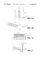
- FIGS. 1A, 1 B and 1 Care schematic views of normal or oblique illumination beams illuminating a surface with a particle thereon useful for illustrating the invention.
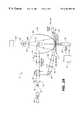
- FIG. 2Ais a schematic view of a sample inspection system employing an ellipsoidal mirror for illustrating one embodiment of the invention.
- FIG. 2Bis a schematic view of a sample inspection system employing a paraboloidal mirror to illustrate another embodiment of the invention.
- FIG. 3is an exploded simplified view of a portion of the system of FIG. 2A or FIG. 2B to illustrate another aspect of the invention.
- FIG. 4is a schematic view of a sample inspection system employing two different wavelengths for illumination to illustrate yet another embodiment of the invention.
- FIGS. 5A and 5Bare schematic views of sample inspection systems illustrating two different embodiments employing switches for switching a radiation beam between a normal illumination path and an oblique illumination path to illustrate yet another aspect of the invention.
- FIG. 6is a schematic view of a beam illuminating a semiconductor wafer surface to illustrate the effect of a change in height of a wafer on the position of the spot illuminated by beam.
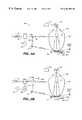
- FIG. 7is a schematic view of a portion of a sample inspection system inspecting a semiconductor wafer, employing three lenses, where the direction of the illumination beam is altered to reduce the error in the position of the illuminated spot caused by the change in height of the wafer.
- FIG. 8is a schematic view of a portion of a sample inspection system employing only one lens to compensate for a change in height of the wafer.
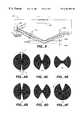
- FIGS. 9A-9Fare schematic views of six different spatial filters useful for detecting anomalies of samples.
- FIG. 10Ais a simplified partially schematic and partially cross-sectional view of a programmable spatial filter employing a layer of liquid crystal material sandwiched between an electrode and an array of electrodes in the shape of sectors of a circle and means for applying a potential difference across at least one sector in the array and the other electrode, so that the portion of the liquid crystal layer adjacent to the at least one sector is controlled to be radiation transparent or scattering.
- FIG. 10Bis a top view of the filter of FIG. 10 A.
- FIG. 1Ais a schematic view of a surface 20 of a sample to be inspected and an illumination beam 22 directed in a direction normal to surface 20 to illuminate the surface and a particle 24 on the surface.
- the illumination beam 22illuminates an area or spot 26 of surface 20 and a detection system (not shown) detects light scattered by particle 24 and by portion or spot 26 of the surface 20 .
- the ratio of the photon flux received by the detector from particle 24 to that from spot 26indicates the sensitivity of the system to particle detection.
- an illumination beam 28 directed at an oblique angle to surface 20is used to illuminate spot 26 ′ and particle 24 instead, as shown in FIG. 1B, from a comparison between FIGS. 1A and 1B, it will be evident that the ratio of the photon flux from the particle 24 to that from the illuminated spot will be greater in the case of the oblique illumination in FIG. 1B compared to that in FIG. 1 A. Therefore, for the same throughput (spots 26 , 26 ′ having the same area), the sensitivity of the oblique incidence beam in detecting small particles is superior and is the method of choice in the detection of small particles.
- FIG. 1Cillustrates an oblique beam 28 ′ illuminating a surface 30 having a pit 32 and particle 24 ′ thereon.
- the pit 32is of comparable size to particle 24 , it will scatter a much smaller amount of photon flux compared to particle 24 from oblique beam 28 ′.
- the pit 32 and particle 24are illuminated by a beam such as 22 directed in a direction normal to surface 30 , pit 32 and particle 24 would cause comparable amount of photon flux scattering.
- anomaly detection employing oblique illuminationis much more sensitive to particles than COPs.
- Azimuthal collection angleis defined as the angle made by the collection direction to the direction of oblique illumination when viewed from the top.
- PCT/US96/15354noted above, are retained, including its uniform scratch sensitivity and the possibility of adding a bright-field channel as described in PCT Patent Application No. PCT/US97/04134, filed Mar. 5, 1997, entitled “Single Laser Bright Field and Dark Field System for Detecting Anomalies of a Sample.”
- FIG. 2Ais a schematic view of a sample inspection system to illustrate a general set up for implementing anomaly detection using both normal and oblique illumination beams.
- a radiation sourcethat provides radiation at one or more wavelengths in a wide electromagnetic spectrum (including but not limited to ultraviolet, visible, infrared) may be used, such as a laser 52 providing a laser beam 54 .
- a lens 56focuses the beam 54 through a spatial filter 58 and lens 60 collimates the beam and conveys it to a polarizing beamsplitter 62 .
- Beamsplitter 62passes a first polarized component to the normal illumination channel and a second polarized component to the oblique illumination channel, where the first and second components are orthogonal.
- the first polarized componentis focused by optics 72 and reflected by mirror 74 towards a sample surface 76 a of a semiconductor wafer 76 .
- the radiation scattered by surface 76 ais collected and focused by an ellipsoidal mirror 78 to a photomultiplier tube 80 .
- the second polarized componentis reflected by beamsplitter 62 to a mirror 82 which reflects such beam through a half-wave plate 84 and focused by optics 86 to surface 76 a .
- Radiation originating from the oblique illumination beam in the oblique channel 90 and scattered by surface 76 ais collected by an ellipsoidal mirror and focused to photomultiplier tube 80 .
- Photomultiplier tube 80has a pinhole entrance 80 a .
- the pinhole 80 a and the illuminated spot(from the normal and oblique illumination channels on surface 76 a ) are preferably at the foci of the ellipsoidal mirror 78 .
- Wafer 76is rotated by a motor 92 which is also moved linearly by transducer 94 , and both movements are controlled by a controller 96 , so that the normal and oblique illumination beams in channels 70 and 90 scan surface 76 a along a spiral scan to cover the entire surface.
- a paraboloidal mirror 78 ′collimates the scattered radiation from surface 76 a into a collimated beam 102 and the collimated beam 102 is then focused by an objective 104 and through an analyzer 98 to the photomultiplier tube 80 .
- the sample inspection system 100is exactly the same as system 50 of FIG. 2 A.
- Curved mirrored surfaces having shapes other than ellipsoidal or paraboloidal shapesmay also be used; preferably, each of such curved mirrored surfaces has an axis of symmetry substantially coaxial with the path of the normal illumination path, and defines an input aperture for receiving scattered radiation. All such variations are within the scope of the invention.
- the motor, transducer and control for moving the semiconductor waferhas been omitted from FIG. 2 B and from FIGS. 4, 5 A, 5 B described below.
- FIGS. 2A and 2Bcan be implemented in different embodiments.
- a half-wave plate(not shown) is added between laser 52 and lens 56 in FIGS. 2A and 2B so that the polarization of the light reaching the beamsplitter 62 can be switched between P and S.
- the beamsplitter 62passes radiation only into the normal channel 70 and no radiation will be directed towards the oblique channel 90 .
- beamsplitter 62passes radiation only into the oblique channel 90 and no radiation will be directed through the normal channel 70 .
- the half-wave plate between laser 52 and lens 56causes radiation from laser 52 to be directed only along the oblique channel 90 and the scanning sequence by means of motor 92 , transducer 94 and control 96 is reversed and data at detector 80 is recorded in a RETURN cycle.
- the data set collected during the GO cycle and that collected during the return cyclemay be compared to provide information concerning the nature of the defects detected.
- a half-wave plate and a polarizing beamsplitteras in FIG.
- the above-described operationmay also be performed by replacing such components with a removable mirror placed in the position of beamsplitter 62 . If the mirror is not present, the radiation beam from laser 52 is directed along the normal channel 70 . When the mirror is present, the beam is then directed along the oblique channel 90 . Such mirror should be accurately positioned to ensure exact registration of the two scans during the GO and RETURN cycles. While simple, the above-described Go and RETURN option requires extra time expended in the RETURN cycle.
- the normal illumination beam 70illuminates a spot on surface 76 a .
- the oblique illumination beam 90also illuminates a spot on the surface 76 a .
- the two illuminated spotsshould have the same shape.
- beam 90has a circular cross-section, it would illuminate an elliptical spot on the surface.
- focusing optics 72comprises a cylindrical lens so that beam 70 has an elliptical cross-section and illuminates also an elliptical spot on surface 76 a .
- FIG. 3is an enlarged view of surface 76 a and the normal and oblique illumination beams 70 , 90 to illustrate an offset 120 between the normal and oblique illumination spots 70 a , 90 a.
- radiation scattered from the two spots 70 a , 90 awould be detected at different times and would be distinguished.
- the method illustrated in FIG. 3causes a reduction in system resolution and increased background scattering due to the presence of both spots.
- the pinholeshould be somewhat enlarged in the direction of the offset.
- detector 80will sense an increased background scattering due to the enlargement of the pinhole 80 a . Since the background is due to both beams whereas the particle scattered radiation is due to one or the other spot, the signal-to-noise ratio is decreased.
- the offsetis not greater than three times the spatial extent, or less than the spatial extent, of the point spread function of either the normal or oblique illumination beam.
- FIG. 4is a schematic view of a sample inspection system employing a normal illumination beam comprising radiation at a first wavelength ⁇ 1 and an oblique illumination beam of radiation of wavelength ⁇ 2 to illustrate another embodiment of the invention.
- the laser 52 of FIGS. 2A, 2 Bmay supply radiation at only one wavelength, such as 488 nm of argon.
- beam 4supplies radiation at at least two different wavelengths in beam 54 ′, such as at 488 and 514 nm, instead of radiation of only one wavelength,
- Such beamis split by a dichroic beamsplitter 162 into a first beam at a first wavelength ⁇ 1 (488 nm) and a second beam of wavelength ⁇ 2 (514 nm), by passing radiation at wavelength ⁇ 1 and reflecting radiation at wavelength ⁇ 2 , for example.
- beam 70 ′ at wavelength ⁇ 1is reflected by mirror 74 towards surface 76 a as the normal illumination beam.
- the reflected radiation of wavelength ⁇ 2 at beamsplitter 162is further reflected by mirror 82 and focused by optics 86 as the oblique illumination beam 90 ′ to illuminate the surface.
- the optics in both the normal and oblique illumination pathsare such that the normal and oblique illuminated spots substantially overlap with no offset there between.
- the radiation scattered by surface 76 aretains the wavelength characteristics of the beams from which the radiation originate, so that the radiation scattered by the surface originating from normal illumination beam 70 ′ can be separated from radiation scattered by the surface originating from oblique illumination beam 90 ′.
- Radiation scattered by surface 76 ais again collected and focused by an ellipsoidal mirror 78 through a pinhole 164 a of a spatial filter 164 to a dichroic beamsplitter 166 .
- beamsplitter 166passes the scattered radiation at wavelength ⁇ 1 to detector 80 ( 1 ) through a lens 168 .
- Dichroic beamsplitter 166reflects scattered radiation at wavelength ⁇ 2 through a lens 170 to photomultiplier tube 80 ( 2 ). Again, the mechanism for causing the wafer to rotate along a spiral path has been omitted from FIG. 4 for simplicity.
- the laser source 52 ′should provide radiation at two distinct wavelengths.
- a commercially available multi-line laser source that may be usedis the 2214-65-ML manufactured by Uniphase, San Jose, Calif.
- the amplitude stability of this laser at any given wavelengthis around 3.5%. If such a laser is used, the scheme in FIG. 4 will be useful for applications such as bare silicon inspection but may have diminished particle detection sensitivity when used to scan rough films.
- FIGS. 5A and 5BYet another option for implementing the arrangements generally shown in FIGS. 2A and 2B is illustrated in FIGS. 5A and 5B.
- a radiation beamis switched between the normal and oblique illumination channels at a higher frequency than the data collection rate so that the data collected due to scattering from the normal illumination beam may be distinguished from data collected from scattering due to the oblique illumination channel.
- an electro-optic modulatore.g. a Pockels cell
- the beambeing either transmitted or reflected by the polarizing beamsplitter 62 at the drive frequency of modulator 182 as controlled by a control 184 .
- the electro-optic modulatormay be replaced by a Bragg modulator 192 as shown in FIG. 5B, which may be turned on and off at a high frequency as controlled.
- Modulator 192is powered by block 193 at frequency ⁇ b . This block is turned on and off at a frequency ⁇ m .
- a zero order beam 194 apasses through the Bragg modulator 192 , and becomes the normal illumination beam reflected to surface 76 a by mirror 74 .
- cell 192In the on condition, cell 192 generates a deflected first order beam 194 b , which is reflected by mirrors 196 , 82 to surface 76 a .
- a weak zero order normal illumination beamis still maintained, so that the arrangement in FIG. 5B is not as good as that in FIG. 5 A.
- the electro-optic modulator of FIG. 5 A and the Bragg modulator of FIG. 5Bare operated at a frequency higher than the data rate, and preferably, at a frequency at least about 3 or 5 times the data rate of tube 80 .
- the optics in both the normal and oblique illumination paths of FIGS. 5A, 5 Bare such that the normal and oblique illuminated spots substantially overlap with no offset there between.
- the arrangements in FIGS. 2A, 2 B, 4 , 5 A, 5 Bare advantageous in that the same radiation collector 78 and detector 80 are used for detecting scattered light originating from the normal illumination beam as well as from the oblique illumination beam.
- FIGS. 2A, 2 B, 4 , 5 A, 5 Bmaximize the sensitivity of detection.
- FIGS. 2A, 2 BIn contrast to arrangements where multiple detectors are placed at different azimuthal collection angles relative to the oblique illumination beam, the arrangements of FIGS. 2A, 2 B has superior sensitivity and is simpler in arrangement and operation, since there is no need to synchronize or correlate the different detection channels that would be required in a multiple detector arrangement.
- the ellipsoidal mirror 78collects radiation scattered within the range of at least 25 to 70 ° from the normal direction to the surface which accounts for most of the radiation that is scattered by surface 76 a from an oblique illumination beam, and that contains information useful for particle and COPs detection.
- the three dimensional intensity distribution of scattered radiation from small particles on the surface when the surface is illuminated by a P-polarized illumination beam at or near a grazing angle to the surfacehas the shape of a toroid.
- the curved mirror collectors of FIGS. 2A, 2 B, 4 , 5 A, 5 Bare particularly advantageous for collecting the scattered radiation from small and large particles and directing the scattered radiation towards a detector.
- the intensity distribution of radiation scattered from small particles on surfacesis in the shape of a sphere.
- the collectors in FIGS. 2A, 2 B, 4 , 5 A, 5 Bare also advantageous for collecting such scattered radiation.
- the illumination angle of beam 90is within the range of 45 to 85° from a normal direction to the sample surface, and preferably at 70 or 75°, which is close to the principal angle of silicon at 488 and 514 nm, and would allow the beam passage to be unhindered by the walls of the collector.
- the particle photon fluxis enhanced as illustrated in FIGS. 1A and 1B and the discrimination against the pits is substantial.
- a prerequisite for the comparison of signals generated by two detection channels for a given defectis the ability to place the two spots on the same location.
- semiconductor wafers or other sample surfacesare not completely flat, nor do they have the same thickness. Such imperfections are of little concern for anomaly detection employing a normal incidence beam, as long as the wafer surface remains within the depth of focus.
- wafer-height variationwill cause the beam position and hence the position of the illuminated spot to be incorrect.
- ⁇is the oblique incidence angle between the beam and a normal direction N to the wafer surface.
- Another alternativeis to move the light source and the detector when the height of the wafer changes so as to maintain a constant height between the light source and the detector on the one hand and the wafer surface at the illuminated spot on the other. This is obviously cumbersome and may be impractical.
- Another aspect of the inventionis based on the observation that, by changing the direction of the illumination beam in response to a detected change in wafer height, it is possible to compensate for the change in wafer height to reduce beam position error caused thereby.
- FIG. 7One scheme for implementing the above aspect is illustrated in FIG. 7 .
- an illumination beamis reflected by a mirror 202 and focused through three lenses L 1 , L 2 , L 3 to the wafer surface 204 a .
- the positions of the lensesare set in order to focus an oblique illumination beam 70 ′′ to wafer surface 204 a in dotted line in FIG. 7 .
- a quad cell (or other type of position sensitive detector) 206is positioned so that the specular reflection 70 a ′′ of the beam 70 ′′ from surface 204 reaches the cell at the null or zero position 206 a of the cell.
- the wafer surfacemoves from position 204 a to 204 b shown in solid line in FIG.
- Detector 206may be constructed in the same manner as that described in U.S. Pat. No. 5,530,550.
- a position error signal output from detector 206 indicating the deviation from the null position in two orthogonal directionsis sent by cell 206 to a control 208 which generates an error signal to a transducer 210 for rotating the mirror 202 so that the specular reflection 70 b ′′ also reaches the cell at the null position 206 a .
- the direction of the illumination beamis altered until the specular reflection reaches the cell at null position, at which point control 208 applies no error signal to the transducer 210 .
- controller 252divides by 2 the amplitude of the position sensing signal at the output of quad cell detector 254 to derive a quotient signal and applies the quotient signal to transducer 210 .
- the transducer 210rotates the mirror by an amount proportional to the amplitude of the quotient signal.
- the new position of the specular reflectioncorresponds to the correct location of the spot.
- the new error signalis now the new reference.
- FIGS. 7 and 8may be used in conjunction with any one of the inspection systems of FIGS. 2A, 2 B, 3 , 4 , 5 A and 5 B, although only the quad cell ( 206 or 254 ) is shown in these figures.
- the radiation collection and detection schemes in such embodimentsretain the information concerning the direction of scattering of the radiation from surface 76 a relative to the oblique illumination channel 90 or 90 ′. This can be exploited for some applications such as rough surface inspection. This can be done by employing a spatial filter which blocks the scattered radiation collected by the curved mirrored surface towards the detector except for at least one area have a wedge shape.
- the normal illumination channelthere is no directional information since both the illumination and scattering are symmetrical about a normal to the surface. In other words, if the normal illumination channel is omitted in the embodiments of FIGS.
- the curved mirrored collector 78 or 78 ′advantageously collects most of the radiation scattered within the toroidal intensity distribution caused by particle scattering to provide an inspection tool of high particle sensitivity.
- the use of a curved mirrored collectorretains the directional scattering information, where such information can be retrieved by employing a spatial filter as described below.
- FIGS. 9A-9Fillustrate six different embodiments of such spatial filters in the shape of butterflies each with two wings.
- the dark or shaded areas (wings) in these figuresrepresent areas that are opaque to or scatters radiation, and the white or unshaded areas represent areas that transmit such radiation.
- the size(s) of the radiation transmissive (white or unshaded) area(s)are determined in each of the filters in FIGS. 9A-9F by the wedge angle ⁇ .
- the wedge angleis 10°
- FIG. 9Bit is 20°.
- the filter in FIG. 9Bis placed at position 300 of FIGS. 2A, 2 B, 4 , 5 A or 5 B where the 20° wedge-shaped area of radiation collection is centered at approximately 90° and 270° azimuthal collection angles relative to the oblique illumination direction, this has the effect of generating a combined output from two detectors, each with a collection angle of 20°, one detector placed to collect radiation between 80 to 100° azimuthal angles as in U.S. Pat. No. 4,898,471, and the other detector to collect radiation between 260 and 280° azimuthal angles.
- the detection scheme of U.S. Pat. No. 4,898,471can be simulated by blocking out also the wedge area between 260 and 280 azimuthal angles.
- the arrangement of this applicationhas the advantage over U.S. Pat. No. 4,898,471 of higher sensitivity since more of the scattered radiation is collected than in such patent, by means of the curved mirror collector 78 , 78 ′. Furthermore, the azimuthal collection angle can be dynamically changed by programming the filter at position 300 in FIGS. 2A, 2 B, 4 , 5 A, 5 B without having to move any detectors, as described below.
- FIGS. 9A-9Eare all in the shape of butterflies with two wings, where the wings are opaque to, or scatter, radiation and the spaces between the wings transmit radiation between the mirrored surfaces and detector 80 .
- spatial filter of the shape shown in FIG. 9Fhaving a single radiation transmissive wedge-shaped area.
- spatial filters having any number of wedge-shaped areas that are radiation transmissive dispersed around a center at various different anglesmay also be used and are within the scope of the invention.
- the spatial filtermay be constructed using corrugated material where the wedge angle ⁇ can be reduced by flattening the corrugated material.
- two or more filterssuch as those in FIGS. 9A-9F may be superimposed upon one another to alter the opaque or scattering and transparent or transmissive areas.
- a liquid crystal spatial filtermay be advantageously used, one embodiment of which is shown in FIGS. 10A and 10B.
- a liquid crystal materialcan be made radiation transmissive or scattering by changing an electrical potential applied across the layer.
- the liquid crystal layermay be placed between a circular electrode 352 and an electrode array 354 in the shape of n sectors of a circle arranged around a center 356 , where n is a positive integer.
- the sectorsare shown in FIG. 10B which is a top view of one embodiment of filter 350 in FIG. 10A
- Adjacent electrode sectors 354 ( i ) and 354 ( i+ 1), i ranging from 1 to n ⁇ 1,are electrically insulated from each other.
- electrodes 354can also be in the shape of triangles. Where electrodes 354 are shaped as isosceles triangles, the array of electrodes 354 arranged around center 356 has the shape of a polygon. Still other shapes for the array 354 are possible.
- ⁇is chosen to be too small, this means that an inordinate amount of space must be devoted to the separation between adjacent sector electrodes to avoid electrical shorting. Too large a value for ⁇ means that the wedge angle ⁇ can only be changed by large increments. Preferably ⁇ is at least about 5°.
- the polarization state of the beamdoes not, to first order, affect detection.
- the polarization state of the beamcan significantly affect detection sensitivity.
- S polarized radiationFor rough film inspection, it may be desirable to employ S polarized radiation, whereas for smooth surface inspection, S or P polarized radiation may be preferable.
- the resultsmay be compared to yield information for distinguishing between particles and COPs.
- the intensity of the scattered radiation originating from the oblique channel(e.g., in ppm) may be plotted against that originating from the normal channel, and the plot is analyzed. Or a ratio between the two intensities is obtained for each of one or more locations on the sample surface.
- Such operationsmay be performed by a processor 400 in FIGS. 2A, 2 B, 4 , 5 A, 5 B.
- the normal illumination beammay be replaced by one that is not exactly normal to the surface, while retaining most of the advantages of the invention described above.
- such beammay be at a small angle to the normal direction, where the small angle is no more than 10° to the normal direction.
Landscapes
- Physics & Mathematics (AREA)
- General Physics & Mathematics (AREA)
- General Health & Medical Sciences (AREA)
- Chemical & Material Sciences (AREA)
- Analytical Chemistry (AREA)
- Biochemistry (AREA)
- Life Sciences & Earth Sciences (AREA)
- Health & Medical Sciences (AREA)
- Immunology (AREA)
- Pathology (AREA)
- Spectroscopy & Molecular Physics (AREA)
- Investigating Materials By The Use Of Optical Means Adapted For Particular Applications (AREA)
- Testing Or Measuring Of Semiconductors Or The Like (AREA)
- Investigating Or Analysing Materials By Optical Means (AREA)
Abstract
Description
Claims (51)
Priority Applications (21)
| Application Number | Priority Date | Filing Date | Title |
|---|---|---|---|
| US08/933,771US6201601B1 (en) | 1997-09-19 | 1997-09-19 | Sample inspection system |
| US10/070,079US6891611B1 (en) | 1997-09-19 | 1998-09-18 | Sample inspection system |
| PCT/US1998/019564WO1999014575A1 (en) | 1997-09-19 | 1998-09-18 | Improved sample inspection system |
| AU94000/98AAU9400098A (en) | 1997-09-19 | 1998-09-18 | Improved sample inspection system |
| DE69840532TDE69840532D1 (en) | 1997-09-19 | 1998-09-18 | Improved test system for samples |
| DE69819929TDE69819929T2 (en) | 1997-09-19 | 1998-09-18 | IMPROVED TESTING SYSTEM FOR SAMPLES |
| EP02012062AEP1265063B1 (en) | 1997-09-19 | 1998-09-18 | Improved sample inspection system |
| JP2000512065AJP4499279B2 (en) | 1997-09-19 | 1998-09-18 | Improved sample inspection system |
| EP04024371AEP1508799B1 (en) | 1997-09-19 | 1998-09-18 | Improved sample inspection system |
| DE69828827TDE69828827T2 (en) | 1997-09-19 | 1998-09-18 | Improved test system for samples |
| EP98947155AEP1023582B1 (en) | 1997-09-19 | 1998-09-18 | Improved sample inspection system |
| US09/746,415US6657715B2 (en) | 1997-09-19 | 2000-12-21 | Sample inspection system |
| US09/746,141US6639662B2 (en) | 1997-09-19 | 2000-12-21 | Sample inspection system |
| US09/745,492US6384910B2 (en) | 1997-09-19 | 2000-12-21 | Sample inspection system |
| US09/891,693US6956644B2 (en) | 1997-09-19 | 2001-06-26 | Systems and methods for a wafer inspection system using multiple angles and multiple wavelength illumination |
| US10/033,069US6618134B2 (en) | 1997-09-19 | 2001-12-27 | Sample inspection system |
| US10/437,829US7079238B2 (en) | 1997-09-19 | 2003-05-13 | Sample inspection system |
| US10/627,402US7064821B2 (en) | 1997-09-19 | 2003-07-24 | Sample inspection system |
| US11/007,729US7119897B2 (en) | 1997-09-19 | 2004-12-07 | Sample inspection system |
| US11/126,467US20050206886A1 (en) | 1997-09-19 | 2005-05-10 | Sample inspection system |
| US11/227,555US7218392B2 (en) | 1997-09-19 | 2005-09-14 | Systems and methods for a wafer inspection system using multiple angles and multiple wavelength illumination |
Applications Claiming Priority (1)
| Application Number | Priority Date | Filing Date | Title |
|---|---|---|---|
| US08/933,771US6201601B1 (en) | 1997-09-19 | 1997-09-19 | Sample inspection system |
Related Child Applications (6)
| Application Number | Title | Priority Date | Filing Date |
|---|---|---|---|
| US09/070,079ContinuationUS6076211A (en) | 1998-04-30 | 1998-04-30 | Seat cushion with marker |
| PCT/US1998/019564ContinuationWO1999014575A1 (en) | 1997-09-19 | 1998-09-18 | Improved sample inspection system |
| US10/070,079ContinuationUS6891611B1 (en) | 1997-09-19 | 1998-09-18 | Sample inspection system |
| US09/746,141ContinuationUS6639662B2 (en) | 1997-09-19 | 2000-12-21 | Sample inspection system |
| US09/746,415DivisionUS6657715B2 (en) | 1997-09-19 | 2000-12-21 | Sample inspection system |
| US09/745,492DivisionUS6384910B2 (en) | 1997-09-19 | 2000-12-21 | Sample inspection system |
Publications (1)
| Publication Number | Publication Date |
|---|---|
| US6201601B1true US6201601B1 (en) | 2001-03-13 |
Family
ID=25464477
Family Applications (9)
| Application Number | Title | Priority Date | Filing Date |
|---|---|---|---|
| US08/933,771Expired - LifetimeUS6201601B1 (en) | 1997-09-19 | 1997-09-19 | Sample inspection system |
| US10/070,079Expired - Fee RelatedUS6891611B1 (en) | 1997-09-19 | 1998-09-18 | Sample inspection system |
| US09/746,141Expired - LifetimeUS6639662B2 (en) | 1997-09-19 | 2000-12-21 | Sample inspection system |
| US09/745,492Expired - LifetimeUS6384910B2 (en) | 1997-09-19 | 2000-12-21 | Sample inspection system |
| US09/746,415Expired - LifetimeUS6657715B2 (en) | 1997-09-19 | 2000-12-21 | Sample inspection system |
| US10/033,069Expired - LifetimeUS6618134B2 (en) | 1997-09-19 | 2001-12-27 | Sample inspection system |
| US10/437,829Expired - Fee RelatedUS7079238B2 (en) | 1997-09-19 | 2003-05-13 | Sample inspection system |
| US10/627,402Expired - Fee RelatedUS7064821B2 (en) | 1997-09-19 | 2003-07-24 | Sample inspection system |
| US11/126,467AbandonedUS20050206886A1 (en) | 1997-09-19 | 2005-05-10 | Sample inspection system |
Family Applications After (8)
| Application Number | Title | Priority Date | Filing Date |
|---|---|---|---|
| US10/070,079Expired - Fee RelatedUS6891611B1 (en) | 1997-09-19 | 1998-09-18 | Sample inspection system |
| US09/746,141Expired - LifetimeUS6639662B2 (en) | 1997-09-19 | 2000-12-21 | Sample inspection system |
| US09/745,492Expired - LifetimeUS6384910B2 (en) | 1997-09-19 | 2000-12-21 | Sample inspection system |
| US09/746,415Expired - LifetimeUS6657715B2 (en) | 1997-09-19 | 2000-12-21 | Sample inspection system |
| US10/033,069Expired - LifetimeUS6618134B2 (en) | 1997-09-19 | 2001-12-27 | Sample inspection system |
| US10/437,829Expired - Fee RelatedUS7079238B2 (en) | 1997-09-19 | 2003-05-13 | Sample inspection system |
| US10/627,402Expired - Fee RelatedUS7064821B2 (en) | 1997-09-19 | 2003-07-24 | Sample inspection system |
| US11/126,467AbandonedUS20050206886A1 (en) | 1997-09-19 | 2005-05-10 | Sample inspection system |
Country Status (6)
| Country | Link |
|---|---|
| US (9) | US6201601B1 (en) |
| EP (3) | EP1265063B1 (en) |
| JP (1) | JP4499279B2 (en) |
| AU (1) | AU9400098A (en) |
| DE (3) | DE69840532D1 (en) |
| WO (1) | WO1999014575A1 (en) |
Cited By (176)
| Publication number | Priority date | Publication date | Assignee | Title |
|---|---|---|---|---|
| US20020015146A1 (en)* | 1997-09-22 | 2002-02-07 | Meeks Steven W. | Combined high speed optical profilometer and ellipsometer |
| US20020036771A1 (en)* | 2000-09-26 | 2002-03-28 | Hitachi Electronics Engineering Co., Ltd. | Apparatus and method for inspecting surface of semiconductor wafer or the like |
| US20020041374A1 (en)* | 2000-10-10 | 2002-04-11 | Yoshimasa Ohshima | Apparatus for detecting foreign particle and defect and the same method |
| US20020103564A1 (en)* | 2000-09-20 | 2002-08-01 | John Fielden | Methods and systems for determining a composition and a thickness of a specimen |
| US20020107650A1 (en)* | 2000-09-20 | 2002-08-08 | Dan Wack | Methods and systems for determining a critical dimension and a presence of defects on a specimen |
| US20020145740A1 (en)* | 2001-03-26 | 2002-10-10 | Meeks Steven W. | Material independent optical profilometer |
| US20020163634A1 (en)* | 2001-03-26 | 2002-11-07 | Meeks Steven W. | Multiple spot size optical profilometer, ellipsometer, reflectometer and scatterometer |
| US20030011760A1 (en)* | 2001-07-10 | 2003-01-16 | Mehdi Vaez-Iravani | Systems and methods for simultaneous or sequential multi-perspective specimen defect inspection |
| US20030025905A1 (en)* | 2001-03-26 | 2003-02-06 | Meeks Steven W. | Method of detecting and classifying scratches, particles and pits on thin film disks or wafers |
| US6538730B2 (en) | 2001-04-06 | 2003-03-25 | Kla-Tencor Technologies Corporation | Defect detection system |
| US6611328B2 (en)* | 2000-02-24 | 2003-08-26 | Kabushiki Kaisha Topcon | Surface inspecting apparatus and method |
| US6618134B2 (en) | 1997-09-19 | 2003-09-09 | Kla-Tencor Corporation | Sample inspection system |
| US6621570B1 (en)* | 1999-03-04 | 2003-09-16 | Inspex Incorporated | Method and apparatus for inspecting a patterned semiconductor wafer |
| WO2003083560A2 (en) | 2002-03-28 | 2003-10-09 | Kla-Tencor Technologies Corporation | Uv compatible programmable spatial filter |
| US6633375B1 (en)* | 1999-01-29 | 2003-10-14 | Leica Microsystems Semiconductor Gmbh | Method and device for optically examining structured surfaces of objects |
| US20030197874A1 (en)* | 2002-04-19 | 2003-10-23 | Moghaddam Alireza Shahdoost | Method of detecting the thickness of thin film disks or wafers |
| US6673637B2 (en) | 2000-09-20 | 2004-01-06 | Kla-Tencor Technologies | Methods and systems for determining a presence of macro defects and overlay of a specimen |
| US6686995B2 (en) | 2002-03-28 | 2004-02-03 | Kla-Tencor Technologies Corporation | Two-dimensional UV compatible programmable spatial filter |
| US6694284B1 (en) | 2000-09-20 | 2004-02-17 | Kla-Tencor Technologies Corp. | Methods and systems for determining at least four properties of a specimen |
| US6704101B1 (en)* | 2002-01-16 | 2004-03-09 | Advanced Micro Devices, Inc. | Scatterometry based measurements of a moving substrate |
| US20040046959A1 (en)* | 1997-09-22 | 2004-03-11 | Meeks Steven W. | System and method for simultaneously measuring thin film layer thickness, reflectivity, roughness, surface profile and magnetic pattern on thin film magnetic disks and silicon wafers |
| US20040057045A1 (en)* | 2000-12-21 | 2004-03-25 | Mehdi Vaez-Iravani | Sample inspection system |
| US6717671B1 (en) | 1997-09-22 | 2004-04-06 | Candela Instruments | System for simultaneously measuring thin film layer thickness, reflectivity, roughness, surface profile and magnetic pattern |
| WO2003062800A3 (en)* | 2002-01-16 | 2004-04-08 | Lockheed Corp | Portable system and method for determining one or more reflectance properties of a surface |
| US20040085532A1 (en)* | 2000-05-04 | 2004-05-06 | Wayne Chen | System and methods for classifying anomalies of sample surfaces |
| US6757056B1 (en) | 2001-03-26 | 2004-06-29 | Candela Instruments | Combined high speed optical profilometer and ellipsometer |
| US20040125368A1 (en)* | 2002-09-13 | 2004-07-01 | Mehdi Vaez-Iravani | Inspection system for integrated applications |
| US6774987B2 (en) | 1999-01-13 | 2004-08-10 | Nikon Corporation | Surface inspection method, surface inspection apparatus, and recording medium and data signal for providing surface inspection program |
| US6774991B1 (en)* | 1999-05-27 | 2004-08-10 | Inspex Incorporated | Method and apparatus for inspecting a patterned semiconductor wafer |
| US20040169850A1 (en)* | 1999-07-02 | 2004-09-02 | Meeks Steven W. | System and method for double sided optical inspection of thin film disks or wafers |
| US20040169849A1 (en)* | 2002-02-26 | 2004-09-02 | Syunsuke Kimura | Surface foreign matter inspecting device |
| US6812045B1 (en) | 2000-09-20 | 2004-11-02 | Kla-Tencor, Inc. | Methods and systems for determining a characteristic of a specimen prior to, during, or subsequent to ion implantation |
| US20040235205A1 (en)* | 2000-09-20 | 2004-11-25 | Kla-Tencor, Inc. | Methods and systems for determining a critical dimension and overlay of a specimen |
| US20040235206A1 (en)* | 2003-05-19 | 2004-11-25 | Kla-Tencor Technologies Corporation | Apparatus and methods for enabling robust separation between signals of interest and noise |
| US20040246476A1 (en)* | 2003-06-06 | 2004-12-09 | Bevis Christopher F. | Systems for inspection of patterned or unpatterned wafers and other specimen |
| US20050007580A1 (en)* | 2003-07-10 | 2005-01-13 | Macgibbon Bruce | Method and apparatus for locating/sizing contaminants on a polished planar surface of a dielectric or semiconductor material |
| US20050018179A1 (en)* | 2003-07-23 | 2005-01-27 | Kla-Tencor Technologies Corporation | Darkfield inspection system having a programmable light selection array |
| US20050024632A1 (en)* | 2003-07-18 | 2005-02-03 | Plemmons Mark P. | Detection of a wafer edge using collimated light |
| KR100495710B1 (en)* | 2001-12-04 | 2005-06-14 | 가부시키가이샤 토프콘 | Surface inspection system |
| US20050134841A1 (en)* | 1998-09-18 | 2005-06-23 | Mehdi Vacz-Iravani | Sample inspection system |
| US6919957B2 (en) | 2000-09-20 | 2005-07-19 | Kla-Tencor Technologies Corp. | Methods and systems for determining a critical dimension, a presence of defects, and a thin film characteristic of a specimen |
| US20050179891A1 (en)* | 2002-07-29 | 2005-08-18 | Gilad Almogy | Process and assmebly for non-destructive surface inspection |
| US6956644B2 (en)* | 1997-09-19 | 2005-10-18 | Kla-Tencor Technologies Corporation | Systems and methods for a wafer inspection system using multiple angles and multiple wavelength illumination |
| US20050259246A1 (en)* | 2004-05-21 | 2005-11-24 | Tae-Soo Kang | Apparatus for inspecting a surface and methods thereof |
| US20050270530A1 (en)* | 2004-06-04 | 2005-12-08 | Sharp Kabushiki Kaisha | Optical object discriminating device |
| US20060007434A1 (en)* | 2004-07-12 | 2006-01-12 | Dov Furman | Multi mode inspection method and apparatus |
| US20060109457A1 (en)* | 2004-10-04 | 2006-05-25 | Miller Lawrence R | Surface inspection system with improved capabilities |
| US7075741B1 (en) | 2004-06-14 | 2006-07-11 | Kla Tencor Technologues Corporation | System and method for automatically determining magnetic eccentricity of a disk |
| US20060193506A1 (en)* | 2005-02-28 | 2006-08-31 | Negevtech Ltd. | Method and apparatus for detecting defects in wafers including alignment of the wafer images so as to induce the same smear in all images |
| US20060193507A1 (en)* | 2005-02-28 | 2006-08-31 | Negevtech Ltd. | Method and apparatus for detecting defects in wafers |
| US7106425B1 (en) | 2000-09-20 | 2006-09-12 | Kla-Tencor Technologies Corp. | Methods and systems for determining a presence of defects and a thin film characteristic of a specimen |
| US7123357B2 (en) | 1997-09-22 | 2006-10-17 | Candela Instruments | Method of detecting and classifying scratches and particles on thin film disks or wafers |
| US7130036B1 (en) | 2003-09-16 | 2006-10-31 | Kla-Tencor Technologies Corp. | Methods and systems for inspection of an entire wafer surface using multiple detection channels |
| US7130029B2 (en) | 2000-09-20 | 2006-10-31 | Kla-Tencor Technologies Corp. | Methods and systems for determining an adhesion characteristic and a thickness of a specimen |
| US20060244958A1 (en)* | 2003-01-15 | 2006-11-02 | Negevtech Ltd. | System for detection of wafer defects |
| US20060274304A1 (en)* | 2005-06-06 | 2006-12-07 | Haller Kurt L | Systems and methods for inspecting an edge of a specimen |
| US20060285112A1 (en)* | 2005-06-16 | 2006-12-21 | Juergen Reich | Methods and systems for determining drift in a position of a light beam with respect to a chuck |
| EP1746653A1 (en) | 2005-07-22 | 2007-01-24 | Commissariat A L'energie Atomique | Method of fabrication of background noise standards, containing nanostructures on an insulating thin film. |
| US20070024998A1 (en)* | 2004-12-19 | 2007-02-01 | Bills Richard E | System and method for inspecting a workpiece surface by analyzing scattered light in a front quartersphere region above the workpiece |
| US7184138B1 (en)* | 2004-03-11 | 2007-02-27 | Kla Tencor Technologies Corporation | Spatial filter for sample inspection system |
| US7201799B1 (en) | 2004-11-24 | 2007-04-10 | Kla-Tencor Technologies Corporation | System and method for classifying, detecting, and counting micropipes |
| US20070081151A1 (en)* | 2005-10-06 | 2007-04-12 | David Shortt | Methods and systems for inspection of a wafer |
| US20070103676A1 (en)* | 1994-03-24 | 2007-05-10 | Kla-Tencor Corporation | Process and Assembly for Non-Destructive Surface Inspections |
| US7227628B1 (en) | 2003-10-10 | 2007-06-05 | Kla-Tencor Technologies Corp. | Wafer inspection systems and methods for analyzing inspection data |
| US20070132987A1 (en)* | 2005-12-14 | 2007-06-14 | Haller Kurt L | Systems and methods for inspecting a wafer with increased sensitivity |
| US20070145995A1 (en)* | 2004-07-01 | 2007-06-28 | Sopori Bhushan L | Optic probe for semiconductor characterization |
| US20070182958A1 (en)* | 2006-02-08 | 2007-08-09 | Yuji Manabe | Apparatus and method for wafer surface defect inspection |
| US7274445B1 (en)* | 2005-03-11 | 2007-09-25 | Kla-Tencor Technologies Corporation | Confocal scatterometer and method for single-sided detection of particles and defects on a transparent wafer or disk |
| US20070229809A1 (en)* | 2006-04-04 | 2007-10-04 | Kla-Tencor Technologies Corp. | Computer-Implemented Methods and Systems for Determining a Configuration for a Light Scattering Inspection System |
| US20070247668A1 (en)* | 2006-04-24 | 2007-10-25 | Negevtech Of Rehovot | Printed fourier filtering in optical inspection tools |
| US20070252976A1 (en)* | 2006-04-26 | 2007-11-01 | Siemens Aktiengesellschaft | Optical sensor and method for optically inspecting surfaces |
| US7304310B1 (en) | 2003-11-21 | 2007-12-04 | Kla-Tencor Technologies Corp. | Methods and systems for inspecting a specimen using light scattered in different wavelength ranges |
| US20080007727A1 (en)* | 2006-07-07 | 2008-01-10 | Hitachi High-Technologies Corporation | Surface inspection method and surface inspection apparatus |
| US20080018887A1 (en)* | 2006-05-22 | 2008-01-24 | David Chen | Methods and systems for detecting pinholes in a film formed on a wafer or for monitoring a thermal process tool |
| US7349090B2 (en) | 2000-09-20 | 2008-03-25 | Kla-Tencor Technologies Corp. | Methods and systems for determining a property of a specimen prior to, during, or subsequent to lithography |
| US20080117415A1 (en)* | 2001-03-01 | 2008-05-22 | Akira Hamamatsu | Apparatus and method for inspecting defects |
| US20080129988A1 (en)* | 2006-12-05 | 2008-06-05 | Jason Saito | Methods and systems for identifying defect types on a wafer |
| US7396022B1 (en) | 2004-09-28 | 2008-07-08 | Kla-Tencor Technologies Corp. | System and method for optimizing wafer flatness at high rotational speeds |
| US20080218747A1 (en)* | 2004-05-12 | 2008-09-11 | Stokowski Stanley E | Method and Apparatus for Detecting Surface Characteristics on a Mask Blank |
| US20080266547A1 (en)* | 2007-04-24 | 2008-10-30 | Bryan Clark | Scatterometer-interferometer and method for detecting and distinguishing characteristics of surface artifacts |
| US7463349B1 (en)* | 2006-06-02 | 2008-12-09 | Kla-Tencor Technologies Corp. | Systems and methods for determining a characteristic of a specimen |
| US20080304069A1 (en)* | 2007-06-06 | 2008-12-11 | Christian Wolters | Systems and methods for inspecting a specimen with light at varying power levels |
| US20090037134A1 (en)* | 2007-07-30 | 2009-02-05 | Ashok Kulkarni | Semiconductor device property extraction, generation, visualization, and monitoring methods |
| US20090040525A1 (en)* | 2007-08-10 | 2009-02-12 | Azmi Kadkly | Systems configured to inspect a wafer |
| US20090187354A1 (en)* | 2008-01-11 | 2009-07-23 | Masami Ooyama | Inspection apparatus and inspection method |
| US20090276164A1 (en)* | 2006-06-27 | 2009-11-05 | Ichiro Hirata | Board or electronic component warp analyzing method, board or electronic component warp analyzing system and board or electronic component warp analyzing program |
| US7623229B1 (en) | 2008-10-07 | 2009-11-24 | Kla-Tencor Corporation | Systems and methods for inspecting wafers |
| US20090299655A1 (en)* | 2008-05-28 | 2009-12-03 | Stephen Biellak | Systems and methods for determining two or more characteristics of a wafer |
| US20100060888A1 (en)* | 2008-07-24 | 2010-03-11 | Kla-Tencor Corporation | Computer-implemented methods for inspecting and/or classifying a wafer |
| US7684032B1 (en) | 2005-01-06 | 2010-03-23 | Kla-Tencor Corporation | Multi-wavelength system and method for detecting epitaxial layer defects |
| US20100149662A1 (en)* | 2007-06-19 | 2010-06-17 | Armstrong J Joseph | External beam delivery system for laser dark-field illumination in a catadioptric optical system |
| US20100271626A1 (en)* | 2007-07-04 | 2010-10-28 | Hitachi High-Technologies Corporation | Inspection method and inspection device |
| US20110051132A1 (en)* | 2009-09-02 | 2011-03-03 | Aleksey Petrenko | Method and apparatus for producing and Measuring dynamically focussed, steered, and shaped oblique laser illumination for spinning wafer inspection system |
| US20110075137A1 (en)* | 2007-12-19 | 2011-03-31 | Hitachi High-Technologies Corporation | Defect inspection system |
| US20110170090A1 (en)* | 2002-09-30 | 2011-07-14 | Ron Naftali | Illumination system for optical inspection |
| US20110176137A1 (en)* | 2008-10-11 | 2011-07-21 | Bayer Technology Services Gmbh | Optical Sensor |
| US20110196639A1 (en)* | 2008-06-19 | 2011-08-11 | Kla-Tencor Corporation | Computer-implemented methods, computer-readable media, and systems for determining one or more characteristics of a wafer |
| US8134698B1 (en) | 2008-03-14 | 2012-03-13 | Kla-Tencor Corporation | Dynamic range extension in surface inspection systems |
| US8284394B2 (en) | 2006-02-09 | 2012-10-09 | Kla-Tencor Technologies Corp. | Methods and systems for determining a characteristic of a wafer |
| US20130033704A1 (en)* | 2011-06-29 | 2013-02-07 | Kla-Tencor Corporation | Light source tracking in optical metrology system |
| US20130215404A1 (en)* | 2012-02-21 | 2013-08-22 | Asml Netherlands B.V. | Inspection Apparatus and Method |
| US8520208B1 (en) | 2008-11-21 | 2013-08-27 | Kla-Tencor Corporation | Segmented polarizer for optimizing performance of a surface inspection system |
| US8582094B1 (en) | 2005-04-20 | 2013-11-12 | Kla-Tencor Technologies Corp. | Systems and methods for inspecting specimens including specimens that have a substantially rough uppermost layer |
| US8629384B1 (en) | 2009-10-26 | 2014-01-14 | Kla-Tencor Corporation | Photomultiplier tube optimized for surface inspection in the ultraviolet |
| US20140043603A1 (en)* | 2012-08-10 | 2014-02-13 | Hitachi High-Technologies Corporation | Surface inspecting apparatus having double recipe processing function |
| US8786850B2 (en)* | 2012-10-29 | 2014-07-22 | Kla-Tencor Corporation | Illumination energy management in surface inspection |
| US8823935B1 (en) | 2008-09-10 | 2014-09-02 | Kla-Tencor Corporation | Detecting and classifying surface defects with multiple radiation collectors |
| WO2014165544A1 (en)* | 2013-04-01 | 2014-10-09 | Kla-Tencor Corporation | Photomultiplier tube, image sensor, and an inspection system using a pmt or image sensor |
| US8873596B2 (en) | 2011-07-22 | 2014-10-28 | Kla-Tencor Corporation | Laser with high quality, stable output beam, and long life high conversion efficiency non-linear crystal |
| US8891079B2 (en) | 2010-12-16 | 2014-11-18 | Kla-Tencor Corp. | Wafer inspection |
| KR20140143843A (en)* | 2012-04-12 | 2014-12-17 | 케이엘에이-텐코 코포레이션 | Systems and methods for sample inspection and review |
| US8929406B2 (en) | 2013-01-24 | 2015-01-06 | Kla-Tencor Corporation | 193NM laser and inspection system |
| EP2745312A4 (en)* | 2011-08-15 | 2015-05-06 | Kla Tencor Corp | Large particle detection for multi-spot surface scanning inspection systems |
| US9042006B2 (en) | 2012-09-11 | 2015-05-26 | Kla-Tencor Corporation | Solid state illumination source and inspection system |
| WO2015074642A1 (en)* | 2013-11-22 | 2015-05-28 | Inoex Gmbh | Measuring device and method for measuring test objects |
| WO2015095613A1 (en) | 2013-12-19 | 2015-06-25 | Kla-Tencor Corporation | A low-noise sensor and an inspection system using a low-noise sensor |
| US9151940B2 (en) | 2012-12-05 | 2015-10-06 | Kla-Tencor Corporation | Semiconductor inspection and metrology system using laser pulse multiplier |
| US9188544B2 (en) | 2012-04-04 | 2015-11-17 | Kla-Tencor Corporation | Protective fluorine-doped silicon oxide film for optical components |
| US20150355099A1 (en)* | 2014-06-06 | 2015-12-10 | Hamilton Sundstrand Corporation | Scratch verification apparatus and method |
| US9250178B2 (en) | 2011-10-07 | 2016-02-02 | Kla-Tencor Corporation | Passivation of nonlinear optical crystals |
| US9279774B2 (en) | 2011-07-12 | 2016-03-08 | Kla-Tencor Corp. | Wafer inspection |
| US9293882B2 (en) | 2013-09-10 | 2016-03-22 | Kla-Tencor Corporation | Low noise, high stability, deep ultra-violet, continuous wave laser |
| US9354177B2 (en) | 2013-06-26 | 2016-05-31 | Kla-Tencor Corporation | System and method for defect detection and photoluminescence measurement of a sample |
| US9404873B2 (en) | 2012-03-09 | 2016-08-02 | Kla-Tencor Corp. | Wafer inspection with multi-spot illumination and multiple channels |
| US9410901B2 (en) | 2014-03-17 | 2016-08-09 | Kla-Tencor Corporation | Image sensor, an inspection system and a method of inspecting an article |
| US9419407B2 (en) | 2014-09-25 | 2016-08-16 | Kla-Tencor Corporation | Laser assembly and inspection system using monolithic bandwidth narrowing apparatus |
| US9426400B2 (en) | 2012-12-10 | 2016-08-23 | Kla-Tencor Corporation | Method and apparatus for high speed acquisition of moving images using pulsed illumination |
| US9448184B1 (en) | 2012-01-09 | 2016-09-20 | Kla-Tencor Corporation | Method and system for determining one or more optical characteristics of structure of a semiconductor wafer |
| US9494531B2 (en) | 2013-08-09 | 2016-11-15 | Kla-Tencor Corporation | Multi-spot illumination for improved detection sensitivity |
| US9496425B2 (en) | 2012-04-10 | 2016-11-15 | Kla-Tencor Corporation | Back-illuminated sensor with boron layer |
| US20160335772A1 (en)* | 2015-05-11 | 2016-11-17 | Canon Kabushiki Kaisha | Measuring apparatus, measuring method, and program |
| US9509112B2 (en) | 2013-06-11 | 2016-11-29 | Kla-Tencor Corporation | CW DUV laser with improved stability |
| US9525265B2 (en) | 2014-06-20 | 2016-12-20 | Kla-Tencor Corporation | Laser repetition rate multiplier and flat-top beam profile generators using mirrors and/or prisms |
| US9529182B2 (en) | 2013-02-13 | 2016-12-27 | KLA—Tencor Corporation | 193nm laser and inspection system |
| EP2256487A3 (en)* | 2003-09-04 | 2017-03-15 | KLA-Tencor Corporation | Methods for inspection of a specimen using different inspection parameters |
| US9601299B2 (en) | 2012-08-03 | 2017-03-21 | Kla-Tencor Corporation | Photocathode including silicon substrate with boron layer |
| US9608399B2 (en) | 2013-03-18 | 2017-03-28 | Kla-Tencor Corporation | 193 nm laser and an inspection system using a 193 nm laser |
| US20170167986A1 (en)* | 2014-04-25 | 2017-06-15 | Gdt, Inc. | Cosmetic Evaluation Box for Used Electronics |
| US20170205377A1 (en)* | 2014-07-11 | 2017-07-20 | Vanderbilt University | Apparatus and methods for probing a material as a function of depth using depth-dependent second harmonic generation |
| US9748294B2 (en) | 2014-01-10 | 2017-08-29 | Hamamatsu Photonics K.K. | Anti-reflection layer for back-illuminated sensor |
| US9748729B2 (en) | 2014-10-03 | 2017-08-29 | Kla-Tencor Corporation | 183NM laser and inspection system |
| US9767537B1 (en)* | 2016-04-20 | 2017-09-19 | Applied Materials Israel Ltd. | System and method for inspection using programmable filters |
| US9767986B2 (en) | 2014-08-29 | 2017-09-19 | Kla-Tencor Corporation | Scanning electron microscope and methods of inspecting and reviewing samples |
| EP3223001A1 (en)* | 2010-07-13 | 2017-09-27 | Semiconductor Technologies & Instruments Pte Ltd. | System and method for capturing illumination reflected in multiple directions |
| US9793673B2 (en) | 2011-06-13 | 2017-10-17 | Kla-Tencor Corporation | Semiconductor inspection and metrology system using laser pulse multiplier |
| US9804101B2 (en) | 2014-03-20 | 2017-10-31 | Kla-Tencor Corporation | System and method for reducing the bandwidth of a laser and an inspection system and method using a laser |
| US9860466B2 (en) | 2015-05-14 | 2018-01-02 | Kla-Tencor Corporation | Sensor with electrically controllable aperture for inspection and metrology systems |
| US20180045570A1 (en)* | 2015-03-09 | 2018-02-15 | Renishaw Plc | Transmission raman spectroscopy |
| US10082470B2 (en) | 2016-09-27 | 2018-09-25 | Kla-Tencor Corporation | Defect marking for semiconductor wafer inspection |
| US10175555B2 (en) | 2017-01-03 | 2019-01-08 | KLA—Tencor Corporation | 183 nm CW laser and inspection system |
| US10197501B2 (en) | 2011-12-12 | 2019-02-05 | Kla-Tencor Corporation | Electron-bombarded charge-coupled device and inspection systems using EBCCD detectors |
| US10313622B2 (en) | 2016-04-06 | 2019-06-04 | Kla-Tencor Corporation | Dual-column-parallel CCD sensor and inspection systems using a sensor |
| US10324045B2 (en) | 2016-08-05 | 2019-06-18 | Kla-Tencor Corporation | Surface defect inspection with large particle monitoring and laser power control |
| US10462391B2 (en) | 2015-08-14 | 2019-10-29 | Kla-Tencor Corporation | Dark-field inspection using a low-noise sensor |
| US10551320B2 (en) | 2017-01-30 | 2020-02-04 | Kla-Tencor Corporation | Activation of wafer particle defects for spectroscopic composition analysis |
| US10732130B2 (en) | 2018-06-19 | 2020-08-04 | Kla-Tencor Corporation | Embedded particle depth binning based on multiple scattering signals |
| US10748730B2 (en) | 2015-05-21 | 2020-08-18 | Kla-Tencor Corporation | Photocathode including field emitter array on a silicon substrate with boron layer |
| US10778925B2 (en) | 2016-04-06 | 2020-09-15 | Kla-Tencor Corporation | Multiple column per channel CCD sensor architecture for inspection and metrology |
| US10887580B2 (en) | 2016-10-07 | 2021-01-05 | Kla-Tencor Corporation | Three-dimensional imaging for semiconductor wafer inspection |
| US10895452B2 (en) | 2018-09-04 | 2021-01-19 | Asml Netherlands B.V. | Metrology apparatus |
| US10943760B2 (en) | 2018-10-12 | 2021-03-09 | Kla Corporation | Electron gun and electron microscope |
| US11047806B2 (en) | 2016-11-30 | 2021-06-29 | Kla-Tencor Corporation | Defect discovery and recipe optimization for inspection of three-dimensional semiconductor structures |
| US11114489B2 (en) | 2018-06-18 | 2021-09-07 | Kla-Tencor Corporation | Back-illuminated sensor and a method of manufacturing a sensor |
| US11114491B2 (en) | 2018-12-12 | 2021-09-07 | Kla Corporation | Back-illuminated sensor and a method of manufacturing a sensor |
| CN113916904A (en)* | 2021-11-12 | 2022-01-11 | 中国科学技术大学 | Wafer surface defect detection method and detection system |
| US11237455B2 (en) | 2020-06-12 | 2022-02-01 | Kla Corporation | Frequency conversion using stacked strontium tetraborate plates |
| US11379967B2 (en) | 2019-01-18 | 2022-07-05 | Kla Corporation | Methods and systems for inspection of semiconductor structures with automatically generated defect features |
| US11474025B2 (en)* | 2019-03-29 | 2022-10-18 | Tianma Japan, Ltd. | Gas sensing apparatus |
| US11567391B1 (en) | 2021-11-24 | 2023-01-31 | Kla Corporation | Frequency conversion using interdigitated nonlinear crystal gratings |
| US11703460B2 (en) | 2019-07-09 | 2023-07-18 | Kla Corporation | Methods and systems for optical surface defect material characterization |
| US11704887B2 (en) | 2019-09-16 | 2023-07-18 | Assurant, Inc. | System, method, apparatus, and computer program product for utilizing machine learning to process an image of a mobile device to determine a mobile device integrity status |
| DE112022000481T5 (en) | 2021-06-11 | 2023-11-30 | Kla Corporation | TUNABLE DUV LASER ARRANGEMENT |
| US11848350B2 (en) | 2020-04-08 | 2023-12-19 | Kla Corporation | Back-illuminated sensor and a method of manufacturing a sensor using a silicon on insulator wafer |
| US11899338B2 (en) | 2021-12-11 | 2024-02-13 | Kla Corporation | Deep ultraviolet laser using strontium tetraborate for frequency conversion |
| US12045973B2 (en) | 2020-01-06 | 2024-07-23 | Assurant, Inc. | Systems and methods for automatically grading pre-owned electronic devices |
| USRE50340E1 (en) | 2016-03-07 | 2025-03-18 | Assurant, Inc. | Screen damage detection for devices |
Families Citing this family (78)
| Publication number | Priority date | Publication date | Assignee | Title |
|---|---|---|---|---|
| DE19914696C2 (en)* | 1999-03-31 | 2002-11-28 | Fraunhofer Ges Forschung | Device for the rapid measurement of angle-dependent diffraction effects on finely structured surfaces |
| US6587193B1 (en)* | 1999-05-11 | 2003-07-01 | Applied Materials, Inc. | Inspection systems performing two-dimensional imaging with line light spot |
| US6853446B1 (en) | 1999-08-16 | 2005-02-08 | Applied Materials, Inc. | Variable angle illumination wafer inspection system |
| KR100829658B1 (en)* | 1999-08-16 | 2008-05-16 | 어플라이드 머티어리얼스, 인코포레이티드 | Wafer inspection system for irradiation at variable angles |
| US6950182B1 (en)* | 1999-10-18 | 2005-09-27 | J. A. Woollam Co. | Functional equivalent to spatial filter in ellipsometer and the like systems |
| JP4409701B2 (en)* | 2000-02-25 | 2010-02-03 | 株式会社トプコン | Surface inspection device |
| WO2002082064A1 (en)* | 2001-04-06 | 2002-10-17 | Kla-Tencor Corporation | Improved defect detection system |
| US7362425B2 (en)* | 2001-05-18 | 2008-04-22 | Meeks Steven W | Wide spatial frequency topography and roughness measurement |
| US6713753B1 (en)* | 2001-07-03 | 2004-03-30 | Nanometrics Incorporated | Combination of normal and oblique incidence polarimetry for the characterization of gratings |
| US7061627B2 (en)* | 2002-03-13 | 2006-06-13 | Therma-Wave, Inc. | Optical scatterometry of asymmetric lines and structures |
| US20070258085A1 (en)* | 2006-05-02 | 2007-11-08 | Robbins Michael D | Substrate illumination and inspection system |
| US20040038264A1 (en)* | 2002-05-14 | 2004-02-26 | Souza Glauco R. | Fractal dimension analysis of nanoparticle aggregates using angle dependent light scattering for the detection and characterization of nucleic acids and proteins |
| US7137182B2 (en)* | 2002-11-22 | 2006-11-21 | The Boeing Company | Parallel configuration composite material fabricator |
| US8336596B2 (en)* | 2002-11-22 | 2012-12-25 | The Boeing Company | Composite lamination using array of parallel material dispensing heads |
| JP4183492B2 (en)* | 2002-11-27 | 2008-11-19 | 株式会社日立製作所 | Defect inspection apparatus and defect inspection method |
| AU2003290785A1 (en)* | 2003-02-11 | 2004-09-06 | Applied Materials Israel, Ltd. | System and method for inspection of a substrate that has a refractive index |
| US7030978B2 (en) | 2003-04-25 | 2006-04-18 | Applied Materials, Israel, Ltd | System and method for inspection of a substrate that has a refractive index |
| US6872942B1 (en)* | 2003-04-01 | 2005-03-29 | Kla-Tencor Technologies Corporation | High-speed inspection of flat substrates with underlying visible topology |
| DE10323139A1 (en) | 2003-05-22 | 2004-12-23 | Leica Microsystems Jena Gmbh | Method and device for high-resolution fault finding and classification |
| US7365834B2 (en) | 2003-06-24 | 2008-04-29 | Kla-Tencor Technologies Corporation | Optical system for detecting anomalies and/or features of surfaces |
| US7236625B2 (en)* | 2003-07-28 | 2007-06-26 | The Boeing Company | Systems and method for identifying foreign objects and debris (FOD) and defects during fabrication of a composite structure |
| EP1512964A3 (en)* | 2003-09-08 | 2005-03-23 | DaimlerChrysler AG | Procedure and device for determining the road condition with microwaves |
| US7224471B2 (en)* | 2003-10-28 | 2007-05-29 | Timbre Technologies, Inc. | Azimuthal scanning of a structure formed on a semiconductor wafer |
| JP2005156516A (en)* | 2003-11-05 | 2005-06-16 | Hitachi Ltd | Pattern defect inspection method and apparatus |
| US8934702B2 (en)* | 2003-12-02 | 2015-01-13 | The Boeing Company | System and method for determining cumulative tow gap width |
| US7289656B2 (en)* | 2003-12-02 | 2007-10-30 | The Boeing Company | Systems and methods for determining inconsistency characteristics of a composite structure |
| US7319229B2 (en)* | 2003-12-29 | 2008-01-15 | Kla-Tencor Technologies Corporation | Illumination apparatus and methods |
| US7355709B1 (en) | 2004-02-23 | 2008-04-08 | Kla-Tencor Technologies Corp. | Methods and systems for optical and non-optical measurements of a substrate |
| US7039485B2 (en) | 2004-03-12 | 2006-05-02 | The Boeing Company | Systems and methods enabling automated return to and/or repair of defects with a material placement machine |
| US7206066B2 (en)* | 2004-03-19 | 2007-04-17 | Kla-Tencor Technologies Corporation | Reflectance surface analyzer |
| US7193696B2 (en)* | 2004-04-12 | 2007-03-20 | United Technologies Corporation | Systems and methods for using light to indicate defect locations on a composite structure |
| US7593593B2 (en) | 2004-06-16 | 2009-09-22 | Microsoft Corporation | Method and system for reducing effects of undesired signals in an infrared imaging system |
| WO2006002150A1 (en)* | 2004-06-22 | 2006-01-05 | Applied Materials Israel, Ltd. | Wafer inspection system |
| US7315022B1 (en)* | 2004-08-02 | 2008-01-01 | Kla-Tencor Technologies Corporation | High-speed electron beam inspection |
| US20060108048A1 (en)* | 2004-11-24 | 2006-05-25 | The Boeing Company | In-process vision detection of flaws and fod by back field illumination |
| US7424902B2 (en)* | 2004-11-24 | 2008-09-16 | The Boeing Company | In-process vision detection of flaw and FOD characteristics |
| US7889907B2 (en) | 2005-01-12 | 2011-02-15 | The Boeing Company | Apparatus and methods for inspecting tape lamination |
| JP4826750B2 (en)* | 2005-04-08 | 2011-11-30 | オムロン株式会社 | Defect inspection method and defect inspection apparatus using the method |
| US7345825B2 (en) | 2005-06-30 | 2008-03-18 | Kla-Tencor Technologies Corporation | Beam delivery system for laser dark-field illumination in a catadioptric optical system |
| US7394069B1 (en) | 2005-08-30 | 2008-07-01 | Kla-Tencor Technologies Corporation | Large-field scanning of charged particles |
| US7911444B2 (en) | 2005-08-31 | 2011-03-22 | Microsoft Corporation | Input method for surface of interactive display |
| US7435947B2 (en)* | 2005-10-31 | 2008-10-14 | The Boeing Company | Apparatus and methods for integrating encoding functions in material placement machines |
| US7372556B2 (en)* | 2005-10-31 | 2008-05-13 | The Boeing Company | Apparatus and methods for inspecting a composite structure for inconsistencies |
| US20070145267A1 (en)* | 2005-12-12 | 2007-06-28 | Adler David L | Portable scanning electron microscope |
| US20070229833A1 (en)* | 2006-02-22 | 2007-10-04 | Allan Rosencwaig | High-sensitivity surface detection system and method |
| US9068917B1 (en)* | 2006-03-14 | 2015-06-30 | Kla-Tencor Technologies Corp. | Systems and methods for inspection of a specimen |
| EP2008058B1 (en)* | 2006-04-07 | 2012-12-05 | Abbott Medical Optics Inc. | Geometric measurement system and method of measuring a geometric characteristic of an object |
| US20090122304A1 (en)* | 2006-05-02 | 2009-05-14 | Accretech Usa, Inc. | Apparatus and Method for Wafer Edge Exclusion Measurement |
| US20090116727A1 (en)* | 2006-05-02 | 2009-05-07 | Accretech Usa, Inc. | Apparatus and Method for Wafer Edge Defects Detection |
| US7508504B2 (en)* | 2006-05-02 | 2009-03-24 | Accretech Usa, Inc. | Automatic wafer edge inspection and review system |
| US8212857B2 (en)* | 2007-01-26 | 2012-07-03 | Microsoft Corporation | Alternating light sources to reduce specular reflection |
| CA2597891A1 (en)* | 2007-08-20 | 2009-02-20 | Marc Miousset | Multi-beam optical probe and system for dimensional measurement |
| CA2757181C (en) | 2008-04-18 | 2017-10-24 | Coinsecure, Inc. | Apparatus for producing optical signatures from coinage |
| JP5341440B2 (en)* | 2008-09-10 | 2013-11-13 | 株式会社日立ハイテクノロジーズ | Inspection device |
| DE102009000528B4 (en)* | 2009-01-30 | 2011-04-07 | Nanophotonics Ag | Inspection device and method for the optical examination of object surfaces, in particular of wafer surfaces |
| US7907269B2 (en)* | 2009-07-23 | 2011-03-15 | Kla-Tencor Corporation | Scattered light separation |
| CN102230790A (en)* | 2011-03-29 | 2011-11-02 | 上海宏力半导体制造有限公司 | Method for detecting quality of SiGeC (silicon-germanium-carbon) films and method for manufacturing semiconductor devices |
| JP4919307B1 (en)* | 2011-05-13 | 2012-04-18 | レーザーテック株式会社 | Substrate inspection apparatus and mask inspection apparatus |
| CN102322820B (en)* | 2011-09-14 | 2013-07-10 | 西南科技大学 | Automatic separation method for front and rear surface reflected light spots in surface shape detection system |
| US20130077086A1 (en)* | 2011-09-23 | 2013-03-28 | Kla-Tencor Corporation | Solid-State Laser And Inspection System Using 193nm Laser |
| US8998567B2 (en) | 2012-06-08 | 2015-04-07 | General Electric Company | Method, system and apparatus for enhanced off line compressor and turbine cleaning |
| US9670796B2 (en) | 2012-11-07 | 2017-06-06 | General Electric Company | Compressor bellmouth with a wash door |
| US10272475B2 (en) | 2012-11-07 | 2019-04-30 | General, Electric Company | Offline compressor wash systems and methods |
| JP2013210393A (en)* | 2013-07-01 | 2013-10-10 | Hitachi High-Technologies Corp | Defect inspection method and defect inspection apparatus |
| US9941103B2 (en)* | 2013-10-19 | 2018-04-10 | Kla-Tencor Corporation | Bias-variant photomultiplier tube |
| US9927371B2 (en) | 2014-04-22 | 2018-03-27 | Kla-Tencor Corporation | Confocal line inspection optical system |
| TWI495867B (en)* | 2014-07-22 | 2015-08-11 | Machvision Inc | Application of repeated exposure to multiple exposure image blending detection method |
| JP5866586B1 (en)* | 2015-09-22 | 2016-02-17 | マシンビジョンライティング株式会社 | Inspection lighting device and inspection system |
| US11099370B2 (en) | 2016-09-09 | 2021-08-24 | The University Of North Carolina At Chapel Hill | Tilted illumination systems for fluorescence microscopes |
| US10739275B2 (en) | 2016-09-15 | 2020-08-11 | Kla-Tencor Corporation | Simultaneous multi-directional laser wafer inspection |
| CN110100174B (en)* | 2016-10-20 | 2022-01-18 | 科磊股份有限公司 | Hybrid metrology for patterned wafer characterization |
| JP6451821B1 (en)* | 2017-12-05 | 2019-01-16 | マシンビジョンライティング株式会社 | Inspection system and inspection method |
| US11262570B2 (en) | 2018-03-12 | 2022-03-01 | The University Of North Carolina At Chapel Hill | Mirror image microscopy for increased collection |
| US12153227B2 (en) | 2018-03-12 | 2024-11-26 | The University Of North Carolina At Chapel Hill | Light disc microscopy for fluorescence microscopes |
| CN112005100B (en) | 2018-03-12 | 2024-09-20 | 查珀尔希尔北卡罗来纳大学 | Optical disc microscopy for fluorescence microscopy |
| JP7399049B2 (en)* | 2020-08-27 | 2023-12-15 | 信越化学工業株式会社 | Board defect inspection method and defect inspection device |
| US12339235B2 (en) | 2021-11-18 | 2025-06-24 | Onto Innovation Inc. | Simultaneous back and/or front and/or bulk defect detection |
| KR102848747B1 (en)* | 2023-11-01 | 2025-08-22 | (주)넥스틴 | Illumination device and semiconductor inspection apparatus including the same |
Citations (11)
| Publication number | Priority date | Publication date | Assignee | Title |
|---|---|---|---|---|
| US4794265A (en) | 1987-05-08 | 1988-12-27 | Qc Optics, Inc. | Surface pit detection system and method |
| US4893932A (en)* | 1986-05-02 | 1990-01-16 | Particle Measuring Systems, Inc. | Surface analysis system and method |
| US4898471A (en) | 1987-06-18 | 1990-02-06 | Tencor Instruments | Particle detection on patterned wafers and the like |
| US4929845A (en)* | 1989-02-27 | 1990-05-29 | At&T Bell Laboratories | Method and apparatus for inspection of substrates |
| US5389794A (en) | 1992-11-25 | 1995-02-14 | Qc Optics, Inc. | Surface pit and mound detection and discrimination system and method |
| US5416594A (en)* | 1993-07-20 | 1995-05-16 | Tencor Instruments | Surface scanner with thin film gauge |
| US5424838A (en)* | 1993-03-01 | 1995-06-13 | Siu; Bernard | Microelectronics inspection system |
| US5530550A (en) | 1994-12-21 | 1996-06-25 | Tencor Instruments | Optical wafer positioning system |
| WO1997012226A1 (en) | 1995-09-25 | 1997-04-03 | Tencor Instruments | Improved system for surface inspection |
| US5650614A (en)* | 1994-11-29 | 1997-07-22 | Mitsubishi Electric Corporation | Optical scanning system utilizing an atomic force microscope and an optical microscope |
| WO1997033158A1 (en) | 1996-03-05 | 1997-09-12 | Kla-Tencor Corporation | Single laser bright field and dark field system for detecting anomalies of a sample |
Family Cites Families (58)
| Publication number | Priority date | Publication date | Assignee | Title |
|---|---|---|---|---|
| JPS596507B2 (en)* | 1978-03-30 | 1984-02-13 | 株式会社日立製作所 | Foreign object automatic detection device |
| JPS56126747A (en)* | 1980-03-12 | 1981-10-05 | Hitachi Ltd | Inspecting method for flaw, alien substance and the like on surface of sample and device therefor |
| JPS5713340A (en) | 1980-06-27 | 1982-01-23 | Hitachi Ltd | Inspection apparatus for surface defect |
| US4360275A (en) | 1980-08-11 | 1982-11-23 | Litton Systems Inc. | Device for measurement of optical scattering |
| JPS57132044A (en)* | 1981-02-10 | 1982-08-16 | Hitachi Metals Ltd | Discriminating method of surface defect |
| JPS57139607A (en) | 1981-02-23 | 1982-08-28 | Hitachi Ltd | Position measuring equipment |
| US4395126A (en) | 1981-03-12 | 1983-07-26 | Miles Laboratories, Inc. | Apparatus for reflectance measurement of fluorescent radiation and composite useful therein |
| US4378159A (en) | 1981-03-30 | 1983-03-29 | Tencor Instruments | Scanning contaminant and defect detector |
| JPS58113706A (en) | 1981-12-26 | 1983-07-06 | Nippon Kogaku Kk <Nikon> | horizontal position detection device |
| JPS58120106A (en)* | 1982-01-12 | 1983-07-16 | Hitachi Ltd | Semiconductor wafer appearance inspection equipment |
| US4598997A (en) | 1982-02-15 | 1986-07-08 | Rca Corporation | Apparatus and method for detecting defects and dust on a patterned surface |
| US4540286A (en) | 1982-06-03 | 1985-09-10 | Satake Engineering Co., Ltd. | Apparatus for continuously measuring the degree of milling of grains |
| JPS5937693A (en) | 1982-08-25 | 1984-03-01 | 松下電器産業株式会社 | Radio wave seal device |
| US4669875A (en) | 1982-11-04 | 1987-06-02 | Hitachi, Ltd. | Foreign particle detecting method and apparatus |
| DE3422143A1 (en)* | 1984-06-14 | 1985-12-19 | Josef Prof. Dr. Bille | WAFER INSPECTION DEVICE |
| US4740079A (en) | 1984-10-29 | 1988-04-26 | Hitachi, Ltd. | Method of and apparatus for detecting foreign substances |
| GB8621418D0 (en) | 1986-09-05 | 1986-10-15 | Sira Ltd | Inspection apparatus |
| JPS63101737A (en)* | 1986-10-17 | 1988-05-06 | Komatsu Ltd | pattern inspection device |
| JPS63140904A (en) | 1986-12-04 | 1988-06-13 | Toshiba Corp | Scattered light measuring device |
| JP2512878B2 (en)* | 1987-01-29 | 1996-07-03 | 株式会社ニコン | Foreign matter inspection device |
| JPH0769272B2 (en) | 1987-05-18 | 1995-07-26 | 株式会社ニコン | Foreign matter inspection device |
| US4893032A (en)* | 1987-03-23 | 1990-01-09 | International Business Machines Corp. | Non-saturating temperature independent voltage output driver with adjustable down level |
| USRE33956F1 (en) | 1987-06-08 | 1994-06-07 | Optical Specialties Inc | Inspection system for array of microcircuit dies having redundant circuit patterns |
| JPH0820371B2 (en) | 1988-01-21 | 1996-03-04 | 株式会社ニコン | Defect inspection device and defect inspection method |
| JPH01189685A (en) | 1988-01-26 | 1989-07-28 | Seiko Epson Corp | Liquid crystal light valve and video projector with liquid crystal light valve |
| US5058982A (en)* | 1989-06-21 | 1991-10-22 | Orbot Systems Ltd. | Illumination system and inspection apparatus including same |
| JP3053096B2 (en)* | 1989-09-18 | 2000-06-19 | 株式会社日立製作所 | Foreign object detection method and device |
| JPH0695075B2 (en) | 1990-03-16 | 1994-11-24 | 工業技術院長 | Surface texture detection method |
| US5048965A (en)* | 1990-05-02 | 1991-09-17 | At&T Bell Laboratories | Three-dimensional imaging technique with occlusion avoidance |
| DE4123916C2 (en)* | 1990-07-19 | 1998-04-09 | Reinhard Malz | Method and device for dynamic detection and classification of surface features and defects of an object |
| JPH04103144A (en)* | 1990-08-22 | 1992-04-06 | Sharp Corp | Inspection of foreign substance |
| JP2671241B2 (en) | 1990-12-27 | 1997-10-29 | 日立電子エンジニアリング株式会社 | Glass plate foreign matter detection device |
| US5463459A (en) | 1991-04-02 | 1995-10-31 | Hitachi, Ltd. | Method and apparatus for analyzing the state of generation of foreign particles in semiconductor fabrication process |
| US5189481A (en) | 1991-07-26 | 1993-02-23 | Tencor Instruments | Particle detector for rough surfaces |
| US5155372A (en) | 1991-11-26 | 1992-10-13 | International Business Machines Corporation | Optical inspection system utilizing wedge shaped spatial filter |
| US5486919A (en) | 1992-04-27 | 1996-01-23 | Canon Kabushiki Kaisha | Inspection method and apparatus for inspecting a particle, if any, on a substrate having a pattern |
| JP3314440B2 (en) | 1993-02-26 | 2002-08-12 | 株式会社日立製作所 | Defect inspection apparatus and method |
| CH685519A5 (en)* | 1993-03-29 | 1995-07-31 | Tencor Instruments | Method and apparatus for non-destructive surface inspection. |
| JP3246811B2 (en) | 1993-10-18 | 2002-01-15 | 菱電セミコンダクタシステムエンジニアリング株式会社 | Semiconductor wafer inspection equipment |
| JPH07318500A (en)* | 1994-05-23 | 1995-12-08 | Hitachi Ltd | Inspection device near the object surface |
| DE4440261C2 (en) | 1994-11-11 | 1997-04-30 | Wirth Co Kg Masch Bohr | Machine for driving routes, tunnels or the like |
| US5608526A (en) | 1995-01-19 | 1997-03-04 | Tencor Instruments | Focused beam spectroscopic ellipsometry method and system |
| US5712701A (en) | 1995-03-06 | 1998-01-27 | Ade Optical Systems Corporation | Surface inspection system and method of inspecting surface of workpiece |
| US6118525A (en)* | 1995-03-06 | 2000-09-12 | Ade Optical Systems Corporation | Wafer inspection system for distinguishing pits and particles |
| US5962438A (en) | 1995-04-21 | 1999-10-05 | Sumitomo Pharmaceuticals Company, Limited | Estrogen derivative having carriers to bone |
| US5672885A (en) | 1995-07-10 | 1997-09-30 | Qc Optics, Inc. | Surface displacement detection and adjustment system |
| PT101740A (en) | 1995-07-21 | 1996-04-30 | Rar Refinarias Acucar Reunidas | PROCESS FOR REGENERATING IONIC PERFUME RESINS, USED FOR DECORATION OF ACUCAR, USING A SOLUTION OF SACRAROSE CONTAINING CALCIUM HYDROXIDE AND CALCIUM OR SODIUM CHLORIDE. |
| JPH09166549A (en)* | 1995-10-09 | 1997-06-24 | Nkk Corp | Surface inspection equipment |
| US5940175A (en) | 1996-11-01 | 1999-08-17 | Msp Corporation | Method and apparatus for surface inspection in a chamber |
| US6956644B2 (en)* | 1997-09-19 | 2005-10-18 | Kla-Tencor Technologies Corporation | Systems and methods for a wafer inspection system using multiple angles and multiple wavelength illumination |
| US6201601B1 (en) | 1997-09-19 | 2001-03-13 | Kla-Tencor Corporation | Sample inspection system |
| US20040057045A1 (en) | 2000-12-21 | 2004-03-25 | Mehdi Vaez-Iravani | Sample inspection system |
| US5929983A (en) | 1997-10-29 | 1999-07-27 | International Business Machines Corporation | Optical apparatus for determining the height and tilt of a sample surface |
| US6169601B1 (en) | 1998-06-23 | 2001-01-02 | Ade Optical Systems | Method and apparatus for distinguishing particles from subsurface defects on a substrate using polarized light |
| US20050134841A1 (en) | 1998-09-18 | 2005-06-23 | Mehdi Vacz-Iravani | Sample inspection system |
| US6538730B2 (en)* | 2001-04-06 | 2003-03-25 | Kla-Tencor Technologies Corporation | Defect detection system |
| JP4030815B2 (en) | 2001-07-10 | 2008-01-09 | ケーエルエー−テンカー テクノロジィース コーポレイション | System and method for simultaneous or sequential multiple perspective sample defect inspection |
| US6657714B2 (en) | 2001-09-24 | 2003-12-02 | Applied Materials, Inc. | Defect detection with enhanced dynamic range |
- 1997
- 1997-09-19USUS08/933,771patent/US6201601B1/ennot_activeExpired - Lifetime
- 1998
- 1998-09-18EPEP02012062Apatent/EP1265063B1/ennot_activeExpired - Lifetime
- 1998-09-18EPEP04024371Apatent/EP1508799B1/ennot_activeExpired - Lifetime
- 1998-09-18EPEP98947155Apatent/EP1023582B1/ennot_activeExpired - Lifetime
- 1998-09-18JPJP2000512065Apatent/JP4499279B2/ennot_activeExpired - Lifetime
- 1998-09-18DEDE69840532Tpatent/DE69840532D1/ennot_activeExpired - Lifetime
- 1998-09-18USUS10/070,079patent/US6891611B1/ennot_activeExpired - Fee Related
- 1998-09-18WOPCT/US1998/019564patent/WO1999014575A1/enactiveApplication Filing
- 1998-09-18AUAU94000/98Apatent/AU9400098A/ennot_activeAbandoned
- 1998-09-18DEDE69819929Tpatent/DE69819929T2/ennot_activeExpired - Lifetime
- 1998-09-18DEDE69828827Tpatent/DE69828827T2/ennot_activeExpired - Lifetime
- 2000
- 2000-12-21USUS09/746,141patent/US6639662B2/ennot_activeExpired - Lifetime
- 2000-12-21USUS09/745,492patent/US6384910B2/ennot_activeExpired - Lifetime
- 2000-12-21USUS09/746,415patent/US6657715B2/ennot_activeExpired - Lifetime
- 2001
- 2001-12-27USUS10/033,069patent/US6618134B2/ennot_activeExpired - Lifetime
- 2003
- 2003-05-13USUS10/437,829patent/US7079238B2/ennot_activeExpired - Fee Related
- 2003-07-24USUS10/627,402patent/US7064821B2/ennot_activeExpired - Fee Related
- 2005
- 2005-05-10USUS11/126,467patent/US20050206886A1/ennot_activeAbandoned
Patent Citations (13)
| Publication number | Priority date | Publication date | Assignee | Title |
|---|---|---|---|---|
| US4893932A (en)* | 1986-05-02 | 1990-01-16 | Particle Measuring Systems, Inc. | Surface analysis system and method |
| US4893932B1 (en)* | 1986-05-02 | 1992-10-20 | Particle Measuring Syst | |
| US4794265A (en) | 1987-05-08 | 1988-12-27 | Qc Optics, Inc. | Surface pit detection system and method |
| US4898471A (en) | 1987-06-18 | 1990-02-06 | Tencor Instruments | Particle detection on patterned wafers and the like |
| US4929845A (en)* | 1989-02-27 | 1990-05-29 | At&T Bell Laboratories | Method and apparatus for inspection of substrates |
| US5389794A (en) | 1992-11-25 | 1995-02-14 | Qc Optics, Inc. | Surface pit and mound detection and discrimination system and method |
| US5424838A (en)* | 1993-03-01 | 1995-06-13 | Siu; Bernard | Microelectronics inspection system |
| US5416594A (en)* | 1993-07-20 | 1995-05-16 | Tencor Instruments | Surface scanner with thin film gauge |
| US5650614A (en)* | 1994-11-29 | 1997-07-22 | Mitsubishi Electric Corporation | Optical scanning system utilizing an atomic force microscope and an optical microscope |
| US5530550A (en) | 1994-12-21 | 1996-06-25 | Tencor Instruments | Optical wafer positioning system |
| WO1997012226A1 (en) | 1995-09-25 | 1997-04-03 | Tencor Instruments | Improved system for surface inspection |
| WO1997033158A1 (en) | 1996-03-05 | 1997-09-12 | Kla-Tencor Corporation | Single laser bright field and dark field system for detecting anomalies of a sample |
| US5798829A (en)* | 1996-03-05 | 1998-08-25 | Kla-Tencor Corporation | Single laser bright field and dark field system for detecting anomalies of a sample |
Non-Patent Citations (2)
| Title |
|---|
| "Surface Inspection System for Estimation of Wafer," Y. Yatsugake et al., Hitachi Electronics Engineering Technical Report, vol. 11, Jan. 1996, pp. 21-26. |
| Figure, Hitachi Electronics Engineering Co., Ltd., presented by Etsuro Morita of Mitsubishi Materials Silicon Corp. in a presentation entitled "Exploration of COP and COP Defect Crystal Originated "Particles'," at the Sixth International Workshop on 300 Millimeter Wafers on Dec. 5, 1996 in Makuhari, Japan. |
Cited By (357)
| Publication number | Priority date | Publication date | Assignee | Title |
|---|---|---|---|---|
| US20070103676A1 (en)* | 1994-03-24 | 2007-05-10 | Kla-Tencor Corporation | Process and Assembly for Non-Destructive Surface Inspections |
| US7477371B2 (en) | 1994-03-24 | 2009-01-13 | Kla-Tencor Corporation | Process and assembly for non-destructive surface inspections |
| US7064821B2 (en) | 1997-09-19 | 2006-06-20 | Kla-Tencor Technologies Corporation | Sample inspection system |
| US20060007435A1 (en)* | 1997-09-19 | 2006-01-12 | Steve Biellak | Systems and methods for a wafer inspection system using multiple angles and multiple wavelength illumination |
| US6657715B2 (en) | 1997-09-19 | 2003-12-02 | Kla-Tencor Corporation | Sample inspection system |
| US6891611B1 (en)* | 1997-09-19 | 2005-05-10 | Kla- Tencor Corporation | Sample inspection system |
| US7119897B2 (en)* | 1997-09-19 | 2006-10-10 | Kla-Tencor Technologies Corporation | Sample inspection system |
| US7079238B2 (en)* | 1997-09-19 | 2006-07-18 | Kla-Tencor Technologies Corporation | Sample inspection system |
| US20050174568A1 (en)* | 1997-09-19 | 2005-08-11 | Mehdi Vaez-Iravani | Sample inspection system |
| US7218392B2 (en)* | 1997-09-19 | 2007-05-15 | Kla-Tencor Technologies Corporation | Systems and methods for a wafer inspection system using multiple angles and multiple wavelength illumination |
| US6956644B2 (en)* | 1997-09-19 | 2005-10-18 | Kla-Tencor Technologies Corporation | Systems and methods for a wafer inspection system using multiple angles and multiple wavelength illumination |
| US20030206295A1 (en)* | 1997-09-19 | 2003-11-06 | Mehdi Vaez-Iravani | Sample inspection system |
| US6639662B2 (en)* | 1997-09-19 | 2003-10-28 | Kla-Tencor Corporation | Sample inspection system |
| US20050206886A1 (en)* | 1997-09-19 | 2005-09-22 | Mehdi Vaez-Iravani | Sample inspection system |
| US6618134B2 (en) | 1997-09-19 | 2003-09-09 | Kla-Tencor Corporation | Sample inspection system |
| US20050099621A1 (en)* | 1997-09-19 | 2005-05-12 | Mehdi Vaez-Iravani | Sample inspection system |
| US6956660B2 (en) | 1997-09-22 | 2005-10-18 | Kla-Tencor Technologies | System and method for measuring properties of an object using a phase difference between two reflected light signals |
| US20040046959A1 (en)* | 1997-09-22 | 2004-03-11 | Meeks Steven W. | System and method for simultaneously measuring thin film layer thickness, reflectivity, roughness, surface profile and magnetic pattern on thin film magnetic disks and silicon wafers |
| US6956658B2 (en) | 1997-09-22 | 2005-10-18 | Kla-Tencor Technologies Corporation | System and method for measuring object characteristics using phase differences in polarized light reflections |
| US7123357B2 (en) | 1997-09-22 | 2006-10-17 | Candela Instruments | Method of detecting and classifying scratches and particles on thin film disks or wafers |
| US20020015146A1 (en)* | 1997-09-22 | 2002-02-07 | Meeks Steven W. | Combined high speed optical profilometer and ellipsometer |
| US6717671B1 (en) | 1997-09-22 | 2004-04-06 | Candela Instruments | System for simultaneously measuring thin film layer thickness, reflectivity, roughness, surface profile and magnetic pattern |
| US20050134841A1 (en)* | 1998-09-18 | 2005-06-23 | Mehdi Vacz-Iravani | Sample inspection system |
| US6774987B2 (en) | 1999-01-13 | 2004-08-10 | Nikon Corporation | Surface inspection method, surface inspection apparatus, and recording medium and data signal for providing surface inspection program |
| US6633375B1 (en)* | 1999-01-29 | 2003-10-14 | Leica Microsystems Semiconductor Gmbh | Method and device for optically examining structured surfaces of objects |
| US6621570B1 (en)* | 1999-03-04 | 2003-09-16 | Inspex Incorporated | Method and apparatus for inspecting a patterned semiconductor wafer |
| US6774991B1 (en)* | 1999-05-27 | 2004-08-10 | Inspex Incorporated | Method and apparatus for inspecting a patterned semiconductor wafer |
| US20040169850A1 (en)* | 1999-07-02 | 2004-09-02 | Meeks Steven W. | System and method for double sided optical inspection of thin film disks or wafers |
| US7061601B2 (en)* | 1999-07-02 | 2006-06-13 | Kla-Tencor Technologies Corporation | System and method for double sided optical inspection of thin film disks or wafers |
| US6611328B2 (en)* | 2000-02-24 | 2003-08-26 | Kabushiki Kaisha Topcon | Surface inspecting apparatus and method |
| US7038772B2 (en) | 2000-05-04 | 2006-05-02 | Kla-Tencor Corporation | System and methods for classifying anomalies of sample surfaces |
| US20060192951A1 (en)* | 2000-05-04 | 2006-08-31 | Wayne Chen | System and methods for classifying anomalies of sample surfaces |
| US7016031B2 (en) | 2000-05-04 | 2006-03-21 | Kla-Tencor Corporation | System and methods for classifying anomalies of sample surfaces |
| US7315365B2 (en) | 2000-05-04 | 2008-01-01 | Kla-Tencor Corporation | System and methods for classifying anomalies of sample surfaces |
| US20040085532A1 (en)* | 2000-05-04 | 2004-05-06 | Wayne Chen | System and methods for classifying anomalies of sample surfaces |
| US20040169852A1 (en)* | 2000-05-04 | 2004-09-02 | Wayne Chen | System and methods for classifying anomalies of sample surfaces |
| US6946394B2 (en) | 2000-09-20 | 2005-09-20 | Kla-Tencor Technologies | Methods and systems for determining a characteristic of a layer formed on a specimen by a deposition process |
| US7130029B2 (en) | 2000-09-20 | 2006-10-31 | Kla-Tencor Technologies Corp. | Methods and systems for determining an adhesion characteristic and a thickness of a specimen |
| US7139083B2 (en) | 2000-09-20 | 2006-11-21 | Kla-Tencor Technologies Corp. | Methods and systems for determining a composition and a thickness of a specimen |
| US6673637B2 (en) | 2000-09-20 | 2004-01-06 | Kla-Tencor Technologies | Methods and systems for determining a presence of macro defects and overlay of a specimen |
| US7196782B2 (en) | 2000-09-20 | 2007-03-27 | Kla-Tencor Technologies Corp. | Methods and systems for determining a thin film characteristic and an electrical property of a specimen |
| US6782337B2 (en) | 2000-09-20 | 2004-08-24 | Kla-Tencor Technologies Corp. | Methods and systems for determining a critical dimension an a presence of defects on a specimen |
| US6694284B1 (en) | 2000-09-20 | 2004-02-17 | Kla-Tencor Technologies Corp. | Methods and systems for determining at least four properties of a specimen |
| US20040115843A1 (en)* | 2000-09-20 | 2004-06-17 | Kla-Tencor, Inc. | Methods and systems for determining a presence of macro defects and overlay of a specimen |
| US20040092045A1 (en)* | 2000-09-20 | 2004-05-13 | Gary Bultman | Methods and systems for determining a presence of macro and micro defects on a specimen |
| US7751046B2 (en) | 2000-09-20 | 2010-07-06 | Kla-Tencor Technologies Corp. | Methods and systems for determining a critical dimension and overlay of a specimen |
| US20020107650A1 (en)* | 2000-09-20 | 2002-08-08 | Dan Wack | Methods and systems for determining a critical dimension and a presence of defects on a specimen |
| US6806951B2 (en) | 2000-09-20 | 2004-10-19 | Kla-Tencor Technologies Corp. | Methods and systems for determining at least one characteristic of defects on at least two sides of a specimen |
| US6812045B1 (en) | 2000-09-20 | 2004-11-02 | Kla-Tencor, Inc. | Methods and systems for determining a characteristic of a specimen prior to, during, or subsequent to ion implantation |
| US6818459B2 (en) | 2000-09-20 | 2004-11-16 | Kla-Tencor Technologies Corp. | Methods and systems for determining a presence of macro defects and overlay of a specimen |
| US20040073398A1 (en)* | 2000-09-20 | 2004-04-15 | Kla-Tencor, Inc. | Methods and systems for determining a critical dimension and a thin film characteristic of a specimen |
| US20040235205A1 (en)* | 2000-09-20 | 2004-11-25 | Kla-Tencor, Inc. | Methods and systems for determining a critical dimension and overlay of a specimen |
| US7460981B2 (en) | 2000-09-20 | 2008-12-02 | Kla-Tencor Technologies Corp. | Methods and systems for determining a presence of macro and micro defects on a specimen |
| US6829559B2 (en) | 2000-09-20 | 2004-12-07 | K.L.A.-Tencor Technologies | Methods and systems for determining a presence of macro and micro defects on a specimen |
| US6919957B2 (en) | 2000-09-20 | 2005-07-19 | Kla-Tencor Technologies Corp. | Methods and systems for determining a critical dimension, a presence of defects, and a thin film characteristic of a specimen |
| US7349090B2 (en) | 2000-09-20 | 2008-03-25 | Kla-Tencor Technologies Corp. | Methods and systems for determining a property of a specimen prior to, during, or subsequent to lithography |
| US20020179867A1 (en)* | 2000-09-20 | 2002-12-05 | John Fielden | Methods and systems for determining flatness, a presence of defects, and a thin film characteristic of a specimen |
| US6917433B2 (en) | 2000-09-20 | 2005-07-12 | Kla-Tencor Technologies Corp. | Methods and systems for determining a property of a specimen prior to, during, or subsequent to an etch process |
| US8179530B2 (en) | 2000-09-20 | 2012-05-15 | Kla-Tencor Technologies Corp. | Methods and systems for determining a critical dimension and overlay of a specimen |
| US6917419B2 (en) | 2000-09-20 | 2005-07-12 | Kla-Tencor Technologies Corp. | Methods and systems for determining flatness, a presence of defects, and a thin film characteristic of a specimen |
| US7006235B2 (en) | 2000-09-20 | 2006-02-28 | Kla-Tencor Technologies Corp. | Methods and systems for determining overlay and flatness of a specimen |
| US8502979B2 (en) | 2000-09-20 | 2013-08-06 | Kla-Tencor Technologies Corp. | Methods and systems for determining a critical dimension and overlay of a specimen |
| US7106425B1 (en) | 2000-09-20 | 2006-09-12 | Kla-Tencor Technologies Corp. | Methods and systems for determining a presence of defects and a thin film characteristic of a specimen |
| US6891610B2 (en) | 2000-09-20 | 2005-05-10 | Kla-Tencor Technologies Corp. | Methods and systems for determining an implant characteristic and a presence of defects on a specimen |
| US6891627B1 (en) | 2000-09-20 | 2005-05-10 | Kla-Tencor Technologies Corp. | Methods and systems for determining a critical dimension and overlay of a specimen |
| US20020103564A1 (en)* | 2000-09-20 | 2002-08-01 | John Fielden | Methods and systems for determining a composition and a thickness of a specimen |
| US20020190207A1 (en)* | 2000-09-20 | 2002-12-19 | Ady Levy | Methods and systems for determining a characteristic of micro defects on a specimen |
| US20020179864A1 (en)* | 2000-09-20 | 2002-12-05 | John Fielden | Methods and systems for determining a thin film characteristic and an electrical property of a specimen |
| US6950196B2 (en) | 2000-09-20 | 2005-09-27 | Kla-Tencor Technologies Corp. | Methods and systems for determining a thickness of a structure on a specimen and at least one additional property of the specimen |
| US6633831B2 (en) | 2000-09-20 | 2003-10-14 | Kla Tencor Technologies | Methods and systems for determining a critical dimension and a thin film characteristic of a specimen |
| US6798504B2 (en)* | 2000-09-26 | 2004-09-28 | Hitachi High-Tech Electronics Engineering Co., Ltd. | Apparatus and method for inspecting surface of semiconductor wafer or the like |
| US20020036771A1 (en)* | 2000-09-26 | 2002-03-28 | Hitachi Electronics Engineering Co., Ltd. | Apparatus and method for inspecting surface of semiconductor wafer or the like |
| US6731384B2 (en)* | 2000-10-10 | 2004-05-04 | Hitachi, Ltd. | Apparatus for detecting foreign particle and defect and the same method |
| US20020041374A1 (en)* | 2000-10-10 | 2002-04-11 | Yoshimasa Ohshima | Apparatus for detecting foreign particle and defect and the same method |
| US20040057045A1 (en)* | 2000-12-21 | 2004-03-25 | Mehdi Vaez-Iravani | Sample inspection system |
| US7511806B2 (en) | 2001-03-01 | 2009-03-31 | Hitachi High-Tech Electronics Engineering Co., Ltd. | Apparatus and method for inspecting defects |
| US20080117415A1 (en)* | 2001-03-01 | 2008-05-22 | Akira Hamamatsu | Apparatus and method for inspecting defects |
| US6909500B2 (en) | 2001-03-26 | 2005-06-21 | Candela Instruments | Method of detecting and classifying scratches, particles and pits on thin film disks or wafers |
| US20020145740A1 (en)* | 2001-03-26 | 2002-10-10 | Meeks Steven W. | Material independent optical profilometer |
| US6757056B1 (en) | 2001-03-26 | 2004-06-29 | Candela Instruments | Combined high speed optical profilometer and ellipsometer |
| US20050057747A1 (en)* | 2001-03-26 | 2005-03-17 | Meeks Steven W. | Method of detecting and classifying scratches, particles and pits on thin film disks or wafers |
| US20030025905A1 (en)* | 2001-03-26 | 2003-02-06 | Meeks Steven W. | Method of detecting and classifying scratches, particles and pits on thin film disks or wafers |
| US7075630B2 (en) | 2001-03-26 | 2006-07-11 | Kla-Tencor Technologies Corporation | Combined high speed optical profilometer and ellipsometer |
| US20040233419A1 (en)* | 2001-03-26 | 2004-11-25 | Meeks Steven W. | Combined high speed optical profilometer and ellipsometer |
| US7113284B1 (en) | 2001-03-26 | 2006-09-26 | Kla-Tencor Technologies Corporation | Material independent optical profilometer |
| US6897957B2 (en) | 2001-03-26 | 2005-05-24 | Candela Instruments | Material independent optical profilometer |
| US20020163634A1 (en)* | 2001-03-26 | 2002-11-07 | Meeks Steven W. | Multiple spot size optical profilometer, ellipsometer, reflectometer and scatterometer |
| US6862096B2 (en) | 2001-04-06 | 2005-03-01 | Kla-Tencor Corporation | Defect detection system |
| US20030210393A1 (en)* | 2001-04-06 | 2003-11-13 | Kla-Tencor Corporation | Defect detection system |
| US6538730B2 (en) | 2001-04-06 | 2003-03-25 | Kla-Tencor Technologies Corporation | Defect detection system |
| US20050018181A1 (en)* | 2001-04-06 | 2005-01-27 | Mehdi Vaez-Iravani | Defect detection system |
| US20030011760A1 (en)* | 2001-07-10 | 2003-01-16 | Mehdi Vaez-Iravani | Systems and methods for simultaneous or sequential multi-perspective specimen defect inspection |
| US6922236B2 (en)* | 2001-07-10 | 2005-07-26 | Kla-Tencor Technologies Corp. | Systems and methods for simultaneous or sequential multi-perspective specimen defect inspection |
| KR100495710B1 (en)* | 2001-12-04 | 2005-06-14 | 가부시키가이샤 토프콘 | Surface inspection system |
| WO2003062800A3 (en)* | 2002-01-16 | 2004-04-08 | Lockheed Corp | Portable system and method for determining one or more reflectance properties of a surface |
| US6704101B1 (en)* | 2002-01-16 | 2004-03-09 | Advanced Micro Devices, Inc. | Scatterometry based measurements of a moving substrate |
| US6781697B1 (en)* | 2002-01-16 | 2004-08-24 | Lockheed Martin Corporation | Portable system and method for determining one or more reflectance properties of a surface |
| US7046354B2 (en) | 2002-02-26 | 2006-05-16 | Matsushita Electric Industrial Co., Ltd. | Surface foreign matter inspecting device |
| US20040169849A1 (en)* | 2002-02-26 | 2004-09-02 | Syunsuke Kimura | Surface foreign matter inspecting device |
| WO2003083560A2 (en) | 2002-03-28 | 2003-10-09 | Kla-Tencor Technologies Corporation | Uv compatible programmable spatial filter |
| US6686995B2 (en) | 2002-03-28 | 2004-02-03 | Kla-Tencor Technologies Corporation | Two-dimensional UV compatible programmable spatial filter |
| US20030197874A1 (en)* | 2002-04-19 | 2003-10-23 | Moghaddam Alireza Shahdoost | Method of detecting the thickness of thin film disks or wafers |
| US6882437B2 (en) | 2002-04-19 | 2005-04-19 | Kla-Tencor Technologies | Method of detecting the thickness of thin film disks or wafers |
| US7463351B2 (en)* | 2002-07-29 | 2008-12-09 | Applied Materials, Inc. | Process and assembly for non-destructive surface inspection |
| US20050179891A1 (en)* | 2002-07-29 | 2005-08-18 | Gilad Almogy | Process and assmebly for non-destructive surface inspection |
| US7116413B2 (en) | 2002-09-13 | 2006-10-03 | Kla-Tencor Corporation | Inspection system for integrated applications |
| US20040125368A1 (en)* | 2002-09-13 | 2004-07-01 | Mehdi Vaez-Iravani | Inspection system for integrated applications |
| US8134699B2 (en)* | 2002-09-30 | 2012-03-13 | Applied Materials, Inc. | Illumination system for optical inspection |
| US20110170090A1 (en)* | 2002-09-30 | 2011-07-14 | Ron Naftali | Illumination system for optical inspection |
| US7843559B2 (en) | 2003-01-15 | 2010-11-30 | Applied Materials South East Asia Pte. Ltd. | System for detection of wafer defects |
| US20060244958A1 (en)* | 2003-01-15 | 2006-11-02 | Negevtech Ltd. | System for detection of wafer defects |
| US7038773B2 (en)* | 2003-05-19 | 2006-05-02 | Kla-Tencor Technologies Corporation | Apparatus and methods for enabling robust separation between signals of interest and noise |
| US20040235206A1 (en)* | 2003-05-19 | 2004-11-25 | Kla-Tencor Technologies Corporation | Apparatus and methods for enabling robust separation between signals of interest and noise |
| US20040246476A1 (en)* | 2003-06-06 | 2004-12-09 | Bevis Christopher F. | Systems for inspection of patterned or unpatterned wafers and other specimen |
| US7068363B2 (en) | 2003-06-06 | 2006-06-27 | Kla-Tencor Technologies Corp. | Systems for inspection of patterned or unpatterned wafers and other specimen |
| US20050007580A1 (en)* | 2003-07-10 | 2005-01-13 | Macgibbon Bruce | Method and apparatus for locating/sizing contaminants on a polished planar surface of a dielectric or semiconductor material |
| US7002675B2 (en) | 2003-07-10 | 2006-02-21 | Synetics Solutions, Inc. | Method and apparatus for locating/sizing contaminants on a polished planar surface of a dielectric or semiconductor material |
| US20050024632A1 (en)* | 2003-07-18 | 2005-02-03 | Plemmons Mark P. | Detection of a wafer edge using collimated light |
| US7280200B2 (en)* | 2003-07-18 | 2007-10-09 | Ade Corporation | Detection of a wafer edge using collimated light |
| WO2005017952A3 (en)* | 2003-07-23 | 2005-09-09 | Kla Tencor Tech Corp | Darkfield inspection system having a programmable light selection array |
| JP2008519245A (en)* | 2003-07-23 | 2008-06-05 | ケーエルエー−テンカー テクノロジィース コーポレイション | Dark field inspection system with programmable light selection array |
| US20060082767A1 (en)* | 2003-07-23 | 2006-04-20 | Kla-Tencor Technologies Corporation | Darkfield inspection system having a programmable light selection array |
| US7199874B2 (en) | 2003-07-23 | 2007-04-03 | Kla-Tencor Technologies Corporation | Darkfield inspection system having a programmable light selection array |
| US7002677B2 (en)* | 2003-07-23 | 2006-02-21 | Kla-Tencor Technologies Corporation | Darkfield inspection system having a programmable light selection array |
| JP4825423B2 (en)* | 2003-07-23 | 2011-11-30 | ケーエルエー−テンカー コーポレイション | Dark field inspection system with programmable light selection array |
| US20050018179A1 (en)* | 2003-07-23 | 2005-01-27 | Kla-Tencor Technologies Corporation | Darkfield inspection system having a programmable light selection array |
| EP2256487A3 (en)* | 2003-09-04 | 2017-03-15 | KLA-Tencor Corporation | Methods for inspection of a specimen using different inspection parameters |
| US7130036B1 (en) | 2003-09-16 | 2006-10-31 | Kla-Tencor Technologies Corp. | Methods and systems for inspection of an entire wafer surface using multiple detection channels |
| US7417724B1 (en) | 2003-10-10 | 2008-08-26 | Kla-Tencor Technologies Corp. | Wafer inspection systems and methods for analyzing inspection data |
| US7227628B1 (en) | 2003-10-10 | 2007-06-05 | Kla-Tencor Technologies Corp. | Wafer inspection systems and methods for analyzing inspection data |
| US7304310B1 (en) | 2003-11-21 | 2007-12-04 | Kla-Tencor Technologies Corp. | Methods and systems for inspecting a specimen using light scattered in different wavelength ranges |
| US7184138B1 (en)* | 2004-03-11 | 2007-02-27 | Kla Tencor Technologies Corporation | Spatial filter for sample inspection system |
| US20080218747A1 (en)* | 2004-05-12 | 2008-09-11 | Stokowski Stanley E | Method and Apparatus for Detecting Surface Characteristics on a Mask Blank |
| US20050259246A1 (en)* | 2004-05-21 | 2005-11-24 | Tae-Soo Kang | Apparatus for inspecting a surface and methods thereof |
| US20050270530A1 (en)* | 2004-06-04 | 2005-12-08 | Sharp Kabushiki Kaisha | Optical object discriminating device |
| US7349091B2 (en)* | 2004-06-04 | 2008-03-25 | Sharp Kabushiki Kaisha | Optical object discriminating device |
| US7075741B1 (en) | 2004-06-14 | 2006-07-11 | Kla Tencor Technologues Corporation | System and method for automatically determining magnetic eccentricity of a disk |
| US7420669B2 (en)* | 2004-07-01 | 2008-09-02 | Midwest Research Institute | Optic probe for semiconductor characterization |
| US20070145995A1 (en)* | 2004-07-01 | 2007-06-28 | Sopori Bhushan L | Optic probe for semiconductor characterization |
| US7274444B2 (en) | 2004-07-12 | 2007-09-25 | Negevtech Ltd. | Multi mode inspection method and apparatus |
| US20060007434A1 (en)* | 2004-07-12 | 2006-01-12 | Dov Furman | Multi mode inspection method and apparatus |
| US7396022B1 (en) | 2004-09-28 | 2008-07-08 | Kla-Tencor Technologies Corp. | System and method for optimizing wafer flatness at high rotational speeds |
| US20060109457A1 (en)* | 2004-10-04 | 2006-05-25 | Miller Lawrence R | Surface inspection system with improved capabilities |
| US7978323B2 (en) | 2004-10-04 | 2011-07-12 | KLA—Tencor Technologies Corporation | Surface inspection system with improved capabilities |
| US20090116004A1 (en)* | 2004-10-04 | 2009-05-07 | Lawrence Robert Miller | Surface Inspection System with Improved Capabilities |
| US7471382B2 (en) | 2004-10-04 | 2008-12-30 | Kla-Tencor Technologies Corporation | Surface inspection system with improved capabilities |
| US7201799B1 (en) | 2004-11-24 | 2007-04-10 | Kla-Tencor Technologies Corporation | System and method for classifying, detecting, and counting micropipes |
| US10018572B2 (en) | 2004-12-19 | 2018-07-10 | Kla-Tencor Corporation | Front quartersphere scattered light analysis |
| US20070024998A1 (en)* | 2004-12-19 | 2007-02-01 | Bills Richard E | System and method for inspecting a workpiece surface by analyzing scattered light in a front quartersphere region above the workpiece |
| US9110033B2 (en)* | 2004-12-19 | 2015-08-18 | Kla-Tencor Corporation | Front quartersphere scattered light analysis |
| US8553215B2 (en) | 2004-12-19 | 2013-10-08 | Kla-Tencor Corporation | Back quartersphere scattered light analysis |
| US20100110419A1 (en)* | 2004-12-19 | 2010-05-06 | Kla-Tencor Corporation | Front Quartersphere Scattered Light Analysis |
| US9488591B2 (en) | 2004-12-19 | 2016-11-08 | Uster Technologies Ag | Front quartersphere scattered light analysis |
| US7605913B2 (en)* | 2004-12-19 | 2009-10-20 | Kla-Tencor Corporation | System and method for inspecting a workpiece surface by analyzing scattered light in a front quartersphere region above the workpiece |
| US7684032B1 (en) | 2005-01-06 | 2010-03-23 | Kla-Tencor Corporation | Multi-wavelength system and method for detecting epitaxial layer defects |
| US7804993B2 (en) | 2005-02-28 | 2010-09-28 | Applied Materials South East Asia Pte. Ltd. | Method and apparatus for detecting defects in wafers including alignment of the wafer images so as to induce the same smear in all images |
| US20060193506A1 (en)* | 2005-02-28 | 2006-08-31 | Negevtech Ltd. | Method and apparatus for detecting defects in wafers including alignment of the wafer images so as to induce the same smear in all images |
| US20060193507A1 (en)* | 2005-02-28 | 2006-08-31 | Negevtech Ltd. | Method and apparatus for detecting defects in wafers |
| US7813541B2 (en) | 2005-02-28 | 2010-10-12 | Applied Materials South East Asia Pte. Ltd. | Method and apparatus for detecting defects in wafers |
| US7274445B1 (en)* | 2005-03-11 | 2007-09-25 | Kla-Tencor Technologies Corporation | Confocal scatterometer and method for single-sided detection of particles and defects on a transparent wafer or disk |
| US8582094B1 (en) | 2005-04-20 | 2013-11-12 | Kla-Tencor Technologies Corp. | Systems and methods for inspecting specimens including specimens that have a substantially rough uppermost layer |
| US7728965B2 (en) | 2005-06-06 | 2010-06-01 | Kla-Tencor Technologies Corp. | Systems and methods for inspecting an edge of a specimen |
| US20060274304A1 (en)* | 2005-06-06 | 2006-12-07 | Haller Kurt L | Systems and methods for inspecting an edge of a specimen |
| US7511816B2 (en) | 2005-06-16 | 2009-03-31 | Kla-Tencor Technologies Corp. | Methods and systems for determining drift in a position of a light beam with respect to a chuck |
| US20060285112A1 (en)* | 2005-06-16 | 2006-12-21 | Juergen Reich | Methods and systems for determining drift in a position of a light beam with respect to a chuck |
| US7692782B2 (en) | 2005-07-22 | 2010-04-06 | Commissariat A L'energie Atomique | Method for fabricating haze noise standards comprising nano-structures on an insulating thin layer |
| EP1746653A1 (en) | 2005-07-22 | 2007-01-24 | Commissariat A L'energie Atomique | Method of fabrication of background noise standards, containing nanostructures on an insulating thin film. |
| US7554656B2 (en)* | 2005-10-06 | 2009-06-30 | Kla-Tencor Technologies Corp. | Methods and systems for inspection of a wafer |
| US20070081151A1 (en)* | 2005-10-06 | 2007-04-12 | David Shortt | Methods and systems for inspection of a wafer |
| US20070132987A1 (en)* | 2005-12-14 | 2007-06-14 | Haller Kurt L | Systems and methods for inspecting a wafer with increased sensitivity |
| US7372559B2 (en) | 2005-12-14 | 2008-05-13 | Kla-Tencor Technologies Corp. | Systems and methods for inspecting a wafer with increased sensitivity |
| US20090009754A1 (en)* | 2005-12-14 | 2009-01-08 | Kla-Tencor Technologies Corporation | Systems and methods for inspecting a wafer with increased sensitivity |
| US7697129B2 (en) | 2005-12-14 | 2010-04-13 | Kla-Tencor Technologies Corp. | Systems and methods for inspecting a wafer with increased sensitivity |
| US20070182958A1 (en)* | 2006-02-08 | 2007-08-09 | Yuji Manabe | Apparatus and method for wafer surface defect inspection |
| US8284394B2 (en) | 2006-02-09 | 2012-10-09 | Kla-Tencor Technologies Corp. | Methods and systems for determining a characteristic of a wafer |
| US8422010B2 (en) | 2006-02-09 | 2013-04-16 | Kla-Tencor Technologies Corp. | Methods and systems for determining a characteristic of a wafer |
| US7436505B2 (en) | 2006-04-04 | 2008-10-14 | Kla-Tencor Technologies Corp. | Computer-implemented methods and systems for determining a configuration for a light scattering inspection system |
| US20070229809A1 (en)* | 2006-04-04 | 2007-10-04 | Kla-Tencor Technologies Corp. | Computer-Implemented Methods and Systems for Determining a Configuration for a Light Scattering Inspection System |
| US8031931B2 (en) | 2006-04-24 | 2011-10-04 | Applied Materials South East Asia Pte. Ltd. | Printed fourier filtering in optical inspection tools |
| US20070247668A1 (en)* | 2006-04-24 | 2007-10-25 | Negevtech Of Rehovot | Printed fourier filtering in optical inspection tools |
| US7538866B2 (en)* | 2006-04-26 | 2009-05-26 | Siemens Aktiengesellschaft | Optical sensor and method for optically inspecting surfaces |
| US20070252976A1 (en)* | 2006-04-26 | 2007-11-01 | Siemens Aktiengesellschaft | Optical sensor and method for optically inspecting surfaces |
| US7528944B2 (en) | 2006-05-22 | 2009-05-05 | Kla-Tencor Technologies Corporation | Methods and systems for detecting pinholes in a film formed on a wafer or for monitoring a thermal process tool |
| US20080018887A1 (en)* | 2006-05-22 | 2008-01-24 | David Chen | Methods and systems for detecting pinholes in a film formed on a wafer or for monitoring a thermal process tool |
| US7463349B1 (en)* | 2006-06-02 | 2008-12-09 | Kla-Tencor Technologies Corp. | Systems and methods for determining a characteristic of a specimen |
| US20090276164A1 (en)* | 2006-06-27 | 2009-11-05 | Ichiro Hirata | Board or electronic component warp analyzing method, board or electronic component warp analyzing system and board or electronic component warp analyzing program |
| US7864310B2 (en)* | 2006-07-07 | 2011-01-04 | Hitachi High-Technologies Corporation | Surface inspection method and surface inspection apparatus |
| US7616299B2 (en)* | 2006-07-07 | 2009-11-10 | Hitachi High-Technologies Corporation | Surface inspection method and surface inspection apparatus |
| US20080007727A1 (en)* | 2006-07-07 | 2008-01-10 | Hitachi High-Technologies Corporation | Surface inspection method and surface inspection apparatus |
| US20100026996A1 (en)* | 2006-07-07 | 2010-02-04 | Hitachi High-Technologies Corporation | Surface inspection method and surface inspection apparatus |
| US20080129988A1 (en)* | 2006-12-05 | 2008-06-05 | Jason Saito | Methods and systems for identifying defect types on a wafer |
| US7728969B2 (en) | 2006-12-05 | 2010-06-01 | Kla-Tencor Technologies Corp. | Methods and systems for identifying defect types on a wafer |
| US20080266547A1 (en)* | 2007-04-24 | 2008-10-30 | Bryan Clark | Scatterometer-interferometer and method for detecting and distinguishing characteristics of surface artifacts |
| US7671978B2 (en) | 2007-04-24 | 2010-03-02 | Xyratex Technology Limited | Scatterometer-interferometer and method for detecting and distinguishing characteristics of surface artifacts |
| US7787114B2 (en) | 2007-06-06 | 2010-08-31 | Kla-Tencor Technologies Corp. | Systems and methods for inspecting a specimen with light at varying power levels |
| US20080304069A1 (en)* | 2007-06-06 | 2008-12-11 | Christian Wolters | Systems and methods for inspecting a specimen with light at varying power levels |
| US8665536B2 (en)* | 2007-06-19 | 2014-03-04 | Kla-Tencor Corporation | External beam delivery system for laser dark-field illumination in a catadioptric optical system |
| US20100149662A1 (en)* | 2007-06-19 | 2010-06-17 | Armstrong J Joseph | External beam delivery system for laser dark-field illumination in a catadioptric optical system |
| US9007581B2 (en)* | 2007-07-04 | 2015-04-14 | Hitachi High-Technologies Corporation | Inspection method and inspection device |
| US20100271626A1 (en)* | 2007-07-04 | 2010-10-28 | Hitachi High-Technologies Corporation | Inspection method and inspection device |
| US20130010281A1 (en)* | 2007-07-04 | 2013-01-10 | Hitachi High-Technologies Corporation | Inspection method and inspection device |
| US8611639B2 (en) | 2007-07-30 | 2013-12-17 | Kla-Tencor Technologies Corp | Semiconductor device property extraction, generation, visualization, and monitoring methods |
| US20090037134A1 (en)* | 2007-07-30 | 2009-02-05 | Ashok Kulkarni | Semiconductor device property extraction, generation, visualization, and monitoring methods |
| US7746459B2 (en) | 2007-08-10 | 2010-06-29 | Kla-Tencor Technologies Corp. | Systems configured to inspect a wafer |
| US20090040525A1 (en)* | 2007-08-10 | 2009-02-12 | Azmi Kadkly | Systems configured to inspect a wafer |
| US8248592B2 (en)* | 2007-12-19 | 2012-08-21 | Hitachi High-Technologies Corporation | Defect inspection system |
| US20110075137A1 (en)* | 2007-12-19 | 2011-03-31 | Hitachi High-Technologies Corporation | Defect inspection system |
| US8203705B2 (en) | 2008-01-11 | 2012-06-19 | Hitachi-High Technologies Corporation | Inspection apparatus and inspection method |
| US20090187354A1 (en)* | 2008-01-11 | 2009-07-23 | Masami Ooyama | Inspection apparatus and inspection method |
| US8537351B2 (en) | 2008-01-11 | 2013-09-17 | Hitachi-High Technologies Corporation | Inspection apparatus and inspection method |
| US8134698B1 (en) | 2008-03-14 | 2012-03-13 | Kla-Tencor Corporation | Dynamic range extension in surface inspection systems |
| US20090299655A1 (en)* | 2008-05-28 | 2009-12-03 | Stephen Biellak | Systems and methods for determining two or more characteristics of a wafer |
| US7912658B2 (en) | 2008-05-28 | 2011-03-22 | Kla-Tencor Corp. | Systems and methods for determining two or more characteristics of a wafer |
| US20110196639A1 (en)* | 2008-06-19 | 2011-08-11 | Kla-Tencor Corporation | Computer-implemented methods, computer-readable media, and systems for determining one or more characteristics of a wafer |
| US8494802B2 (en) | 2008-06-19 | 2013-07-23 | Kla-Tencor Corp. | Computer-implemented methods, computer-readable media, and systems for determining one or more characteristics of a wafer |
| US20100060888A1 (en)* | 2008-07-24 | 2010-03-11 | Kla-Tencor Corporation | Computer-implemented methods for inspecting and/or classifying a wafer |
| US8269960B2 (en) | 2008-07-24 | 2012-09-18 | Kla-Tencor Corp. | Computer-implemented methods for inspecting and/or classifying a wafer |
| US8823935B1 (en) | 2008-09-10 | 2014-09-02 | Kla-Tencor Corporation | Detecting and classifying surface defects with multiple radiation collectors |
| US7623229B1 (en) | 2008-10-07 | 2009-11-24 | Kla-Tencor Corporation | Systems and methods for inspecting wafers |
| US20110176137A1 (en)* | 2008-10-11 | 2011-07-21 | Bayer Technology Services Gmbh | Optical Sensor |
| US8520208B1 (en) | 2008-11-21 | 2013-08-27 | Kla-Tencor Corporation | Segmented polarizer for optimizing performance of a surface inspection system |
| US9068952B2 (en)* | 2009-09-02 | 2015-06-30 | Kla-Tencor Corporation | Method and apparatus for producing and measuring dynamically focussed, steered, and shaped oblique laser illumination for spinning wafer inspection system |
| US20110051132A1 (en)* | 2009-09-02 | 2011-03-03 | Aleksey Petrenko | Method and apparatus for producing and Measuring dynamically focussed, steered, and shaped oblique laser illumination for spinning wafer inspection system |
| US8629384B1 (en) | 2009-10-26 | 2014-01-14 | Kla-Tencor Corporation | Photomultiplier tube optimized for surface inspection in the ultraviolet |
| EP3223001A1 (en)* | 2010-07-13 | 2017-09-27 | Semiconductor Technologies & Instruments Pte Ltd. | System and method for capturing illumination reflected in multiple directions |
| US8891079B2 (en) | 2010-12-16 | 2014-11-18 | Kla-Tencor Corp. | Wafer inspection |
| US9972959B2 (en) | 2011-06-13 | 2018-05-15 | Kla-Tencor Corporation | Semiconductor inspection and metrology system using laser pulse multiplier |
| US10193293B2 (en) | 2011-06-13 | 2019-01-29 | Kla-Tencor Corporation | Semiconductor inspection and metrology system using laser pulse multiplier |
| US9793673B2 (en) | 2011-06-13 | 2017-10-17 | Kla-Tencor Corporation | Semiconductor inspection and metrology system using laser pulse multiplier |
| US9146156B2 (en)* | 2011-06-29 | 2015-09-29 | Kla-Tencor Corporation | Light source tracking in optical metrology system |
| US20130033704A1 (en)* | 2011-06-29 | 2013-02-07 | Kla-Tencor Corporation | Light source tracking in optical metrology system |
| US9279774B2 (en) | 2011-07-12 | 2016-03-08 | Kla-Tencor Corp. | Wafer inspection |
| US8873596B2 (en) | 2011-07-22 | 2014-10-28 | Kla-Tencor Corporation | Laser with high quality, stable output beam, and long life high conversion efficiency non-linear crystal |
| US9413134B2 (en) | 2011-07-22 | 2016-08-09 | Kla-Tencor Corporation | Multi-stage ramp-up annealing for frequency-conversion crystals |
| US9097683B2 (en) | 2011-07-22 | 2015-08-04 | Kla-Tencor Corporation | Laser with high quality, stable output beam, and long life high conversion efficiency non-linear crystal |
| EP2745312A4 (en)* | 2011-08-15 | 2015-05-06 | Kla Tencor Corp | Large particle detection for multi-spot surface scanning inspection systems |
| US9250178B2 (en) | 2011-10-07 | 2016-02-02 | Kla-Tencor Corporation | Passivation of nonlinear optical crystals |
| US11227770B2 (en) | 2011-10-07 | 2022-01-18 | Kla Corporation | Passivation of nonlinear optical crystals |
| US10283366B2 (en) | 2011-10-07 | 2019-05-07 | Kla-Tencor Corporation | Passivation of nonlinear optical crystals |
| US9459215B2 (en) | 2011-10-07 | 2016-10-04 | Kla-Tencor Corporation | Passivation of nonlinear optical crystals |
| US10197501B2 (en) | 2011-12-12 | 2019-02-05 | Kla-Tencor Corporation | Electron-bombarded charge-coupled device and inspection systems using EBCCD detectors |
| US9448184B1 (en) | 2012-01-09 | 2016-09-20 | Kla-Tencor Corporation | Method and system for determining one or more optical characteristics of structure of a semiconductor wafer |
| US20130215404A1 (en)* | 2012-02-21 | 2013-08-22 | Asml Netherlands B.V. | Inspection Apparatus and Method |
| US20150346609A1 (en)* | 2012-02-21 | 2015-12-03 | Asml Netherlands B.V. | Inspection Apparatus and Method |
| US9222834B2 (en)* | 2012-02-21 | 2015-12-29 | Asml Netherlands B.V. | Inspection apparatus and method |
| US10274370B2 (en)* | 2012-02-21 | 2019-04-30 | Asml Netherlands B.V. | Inspection apparatus and method |
| US9404873B2 (en) | 2012-03-09 | 2016-08-02 | Kla-Tencor Corp. | Wafer inspection with multi-spot illumination and multiple channels |
| US9188544B2 (en) | 2012-04-04 | 2015-11-17 | Kla-Tencor Corporation | Protective fluorine-doped silicon oxide film for optical components |
| US9496425B2 (en) | 2012-04-10 | 2016-11-15 | Kla-Tencor Corporation | Back-illuminated sensor with boron layer |
| US9818887B2 (en) | 2012-04-10 | 2017-11-14 | Kla-Tencor Corporation | Back-illuminated sensor with boron layer |
| US10121914B2 (en) | 2012-04-10 | 2018-11-06 | Kla-Tencor Corporation | Back-illuminated sensor with boron layer |
| US10446696B2 (en) | 2012-04-10 | 2019-10-15 | Kla-Tencor Corporation | Back-illuminated sensor with boron layer |
| KR20140143843A (en)* | 2012-04-12 | 2014-12-17 | 케이엘에이-텐코 코포레이션 | Systems and methods for sample inspection and review |
| US9939386B2 (en)* | 2012-04-12 | 2018-04-10 | KLA—Tencor Corporation | Systems and methods for sample inspection and review |
| US11081310B2 (en) | 2012-08-03 | 2021-08-03 | Kla-Tencor Corporation | Photocathode including silicon substrate with boron layer |
| US10199197B2 (en) | 2012-08-03 | 2019-02-05 | Kla-Tencor Corporation | Photocathode including silicon substrate with boron layer |
| US9601299B2 (en) | 2012-08-03 | 2017-03-21 | Kla-Tencor Corporation | Photocathode including silicon substrate with boron layer |
| US20140043603A1 (en)* | 2012-08-10 | 2014-02-13 | Hitachi High-Technologies Corporation | Surface inspecting apparatus having double recipe processing function |
| US9042006B2 (en) | 2012-09-11 | 2015-05-26 | Kla-Tencor Corporation | Solid state illumination source and inspection system |
| US9194812B2 (en)* | 2012-10-29 | 2015-11-24 | Kla-Tencor Corporation | Illumination energy management in surface inspection |
| US8786850B2 (en)* | 2012-10-29 | 2014-07-22 | Kla-Tencor Corporation | Illumination energy management in surface inspection |
| US9768577B2 (en) | 2012-12-05 | 2017-09-19 | Kla-Tencor Corporation | Semiconductor inspection and metrology system using laser pulse multiplier |
| US9151940B2 (en) | 2012-12-05 | 2015-10-06 | Kla-Tencor Corporation | Semiconductor inspection and metrology system using laser pulse multiplier |
| US9426400B2 (en) | 2012-12-10 | 2016-08-23 | Kla-Tencor Corporation | Method and apparatus for high speed acquisition of moving images using pulsed illumination |
| US9318869B2 (en) | 2013-01-24 | 2016-04-19 | Kla-Tencor Corporation | 193nm laser and inspection system |
| US8929406B2 (en) | 2013-01-24 | 2015-01-06 | Kla-Tencor Corporation | 193NM laser and inspection system |
| US9529182B2 (en) | 2013-02-13 | 2016-12-27 | KLA—Tencor Corporation | 193nm laser and inspection system |
| US9935421B2 (en) | 2013-02-13 | 2018-04-03 | Kla-Tencor Corporation | 193nm laser and inspection system |
| US10439355B2 (en) | 2013-02-13 | 2019-10-08 | Kla-Tencor Corporation | 193nm laser and inspection system |
| US9608399B2 (en) | 2013-03-18 | 2017-03-28 | Kla-Tencor Corporation | 193 nm laser and an inspection system using a 193 nm laser |
| US9620341B2 (en) | 2013-04-01 | 2017-04-11 | Kla-Tencor Corporation | Photomultiplier tube, image sensor, and an inspection system using a PMT or image sensor |
| US9478402B2 (en) | 2013-04-01 | 2016-10-25 | Kla-Tencor Corporation | Photomultiplier tube, image sensor, and an inspection system using a PMT or image sensor |
| WO2014165544A1 (en)* | 2013-04-01 | 2014-10-09 | Kla-Tencor Corporation | Photomultiplier tube, image sensor, and an inspection system using a pmt or image sensor |
| US10044166B2 (en) | 2013-06-11 | 2018-08-07 | Kla-Tencor Corporation | CW DUV laser with improved stability |
| US9509112B2 (en) | 2013-06-11 | 2016-11-29 | Kla-Tencor Corporation | CW DUV laser with improved stability |
| KR20210109061A (en)* | 2013-06-26 | 2021-09-03 | 케이엘에이 코포레이션 | System and method for defect detection and photoluminescence measurement of a sample |
| KR20200093690A (en)* | 2013-06-26 | 2020-08-05 | 케이엘에이 코포레이션 | System and method for defect detection and photoluminescence measurement of a sample |
| US9772289B2 (en) | 2013-06-26 | 2017-09-26 | Kla-Tencor Corporation | System and method for defect detection and photoluminescence measurement of a sample |
| KR20210109062A (en)* | 2013-06-26 | 2021-09-03 | 케이엘에이 코포레이션 | System and method for defect detection and photoluminescence measurement of a sample |
| US9354177B2 (en) | 2013-06-26 | 2016-05-31 | Kla-Tencor Corporation | System and method for defect detection and photoluminescence measurement of a sample |
| US9494531B2 (en) | 2013-08-09 | 2016-11-15 | Kla-Tencor Corporation | Multi-spot illumination for improved detection sensitivity |
| US9293882B2 (en) | 2013-09-10 | 2016-03-22 | Kla-Tencor Corporation | Low noise, high stability, deep ultra-violet, continuous wave laser |
| US9660409B2 (en) | 2013-09-10 | 2017-05-23 | Kla-Tencor Corporation | Low noise, high stability, deep ultra-violet, continuous wave laser |
| DE112014004139B4 (en) | 2013-09-10 | 2023-03-02 | Kla-Tencor Corporation | Low-noise, high-stability, deep-ultraviolet cw laser, inspection system using such a laser, and method for generating deep-ultraviolet cw light in a laser |
| CN105765340B (en)* | 2013-11-22 | 2019-06-14 | 伊诺艾克斯有限公司 | For measuring the Terahertz measuring device and method of test object |
| WO2015074642A1 (en)* | 2013-11-22 | 2015-05-28 | Inoex Gmbh | Measuring device and method for measuring test objects |
| CN105765340A (en)* | 2013-11-22 | 2016-07-13 | 伊诺艾克斯有限公司 | Measuring device and method for measuring test objects |
| WO2015095613A1 (en) | 2013-12-19 | 2015-06-25 | Kla-Tencor Corporation | A low-noise sensor and an inspection system using a low-noise sensor |
| US9347890B2 (en) | 2013-12-19 | 2016-05-24 | Kla-Tencor Corporation | Low-noise sensor and an inspection system using a low-noise sensor |
| US10269842B2 (en) | 2014-01-10 | 2019-04-23 | Hamamatsu Photonics K.K. | Anti-reflection layer for back-illuminated sensor |
| US9748294B2 (en) | 2014-01-10 | 2017-08-29 | Hamamatsu Photonics K.K. | Anti-reflection layer for back-illuminated sensor |
| US9620547B2 (en) | 2014-03-17 | 2017-04-11 | Kla-Tencor Corporation | Image sensor, an inspection system and a method of inspecting an article |
| CN106133911A (en)* | 2014-03-17 | 2016-11-16 | 科磊股份有限公司 | Imageing sensor, checking system and the method for inspection object |
| CN106133911B (en)* | 2014-03-17 | 2020-06-26 | 科磊股份有限公司 | Image sensor, inspection system and method of inspecting an object |
| US9410901B2 (en) | 2014-03-17 | 2016-08-09 | Kla-Tencor Corporation | Image sensor, an inspection system and a method of inspecting an article |
| US10495582B2 (en) | 2014-03-20 | 2019-12-03 | Kla-Tencor Corporation | System and method for reducing the bandwidth of a laser and an inspection system and method using a laser |
| US9804101B2 (en) | 2014-03-20 | 2017-10-31 | Kla-Tencor Corporation | System and method for reducing the bandwidth of a laser and an inspection system and method using a laser |
| US20170167986A1 (en)* | 2014-04-25 | 2017-06-15 | Gdt, Inc. | Cosmetic Evaluation Box for Used Electronics |
| US20150355099A1 (en)* | 2014-06-06 | 2015-12-10 | Hamilton Sundstrand Corporation | Scratch verification apparatus and method |
| US9525265B2 (en) | 2014-06-20 | 2016-12-20 | Kla-Tencor Corporation | Laser repetition rate multiplier and flat-top beam profile generators using mirrors and/or prisms |
| US10044164B2 (en) | 2014-06-20 | 2018-08-07 | Kla-Tencor Corporation | Laser repetition rate multiplier and flat-top beam profile generators using mirrors and/or prisms |
| US10371668B2 (en)* | 2014-07-11 | 2019-08-06 | Vanderbilt University | Apparatus and methods for probing a material as a function of depth using depth-dependent second harmonic generation |
| US20170205377A1 (en)* | 2014-07-11 | 2017-07-20 | Vanderbilt University | Apparatus and methods for probing a material as a function of depth using depth-dependent second harmonic generation |
| US9767986B2 (en) | 2014-08-29 | 2017-09-19 | Kla-Tencor Corporation | Scanning electron microscope and methods of inspecting and reviewing samples |
| US10466212B2 (en) | 2014-08-29 | 2019-11-05 | KLA—Tencor Corporation | Scanning electron microscope and methods of inspecting and reviewing samples |
| DE112015004394B4 (en) | 2014-09-25 | 2024-04-11 | Kla-Tencor Corporation | LASER ARRANGEMENT AND INSPECTION SYSTEM USING A MONOLITHIC APPARATUS TO REDUCE BANDWIDTH |
| US9419407B2 (en) | 2014-09-25 | 2016-08-16 | Kla-Tencor Corporation | Laser assembly and inspection system using monolithic bandwidth narrowing apparatus |
| US9748729B2 (en) | 2014-10-03 | 2017-08-29 | Kla-Tencor Corporation | 183NM laser and inspection system |
| US10199149B2 (en) | 2014-10-03 | 2019-02-05 | Kla-Tencor Corporation | 183NM laser and inspection system |
| US20180045570A1 (en)* | 2015-03-09 | 2018-02-15 | Renishaw Plc | Transmission raman spectroscopy |
| US10876894B2 (en)* | 2015-03-09 | 2020-12-29 | Renishaw Plc | Transmission Raman spectroscopy |
| US10235743B2 (en)* | 2015-05-11 | 2019-03-19 | Canon Kabushiki Kaisha | Measuring apparatus, measuring method, and program |
| US20160335772A1 (en)* | 2015-05-11 | 2016-11-17 | Canon Kabushiki Kaisha | Measuring apparatus, measuring method, and program |
| US9860466B2 (en) | 2015-05-14 | 2018-01-02 | Kla-Tencor Corporation | Sensor with electrically controllable aperture for inspection and metrology systems |
| US10194108B2 (en) | 2015-05-14 | 2019-01-29 | Kla-Tencor Corporation | Sensor with electrically controllable aperture for inspection and metrology systems |
| US10748730B2 (en) | 2015-05-21 | 2020-08-18 | Kla-Tencor Corporation | Photocathode including field emitter array on a silicon substrate with boron layer |
| US10462391B2 (en) | 2015-08-14 | 2019-10-29 | Kla-Tencor Corporation | Dark-field inspection using a low-noise sensor |
| USRE50340E1 (en) | 2016-03-07 | 2025-03-18 | Assurant, Inc. | Screen damage detection for devices |
| EP4534987A1 (en) | 2016-04-06 | 2025-04-09 | Kla-Tencor Corporation | Dual-column-parallel ccd sensor and inspection systems using sensor |
| US10764527B2 (en) | 2016-04-06 | 2020-09-01 | Kla-Tencor Corporation | Dual-column-parallel CCD sensor and inspection systems using a sensor |
| US10778925B2 (en) | 2016-04-06 | 2020-09-15 | Kla-Tencor Corporation | Multiple column per channel CCD sensor architecture for inspection and metrology |
| US10313622B2 (en) | 2016-04-06 | 2019-06-04 | Kla-Tencor Corporation | Dual-column-parallel CCD sensor and inspection systems using a sensor |
| US9767537B1 (en)* | 2016-04-20 | 2017-09-19 | Applied Materials Israel Ltd. | System and method for inspection using programmable filters |
| US10324045B2 (en) | 2016-08-05 | 2019-06-18 | Kla-Tencor Corporation | Surface defect inspection with large particle monitoring and laser power control |
| US10082470B2 (en) | 2016-09-27 | 2018-09-25 | Kla-Tencor Corporation | Defect marking for semiconductor wafer inspection |
| US10887580B2 (en) | 2016-10-07 | 2021-01-05 | Kla-Tencor Corporation | Three-dimensional imaging for semiconductor wafer inspection |
| US11047806B2 (en) | 2016-11-30 | 2021-06-29 | Kla-Tencor Corporation | Defect discovery and recipe optimization for inspection of three-dimensional semiconductor structures |
| US10175555B2 (en) | 2017-01-03 | 2019-01-08 | KLA—Tencor Corporation | 183 nm CW laser and inspection system |
| US10429719B2 (en) | 2017-01-03 | 2019-10-01 | Kla-Tencor Corporation | 183 nm CW laser and inspection system |
| DE112018000301T5 (en) | 2017-01-03 | 2019-09-12 | Kla-Tencor Corporation | 183 nm CW laser and inspection system |
| US10551320B2 (en) | 2017-01-30 | 2020-02-04 | Kla-Tencor Corporation | Activation of wafer particle defects for spectroscopic composition analysis |
| US11114489B2 (en) | 2018-06-18 | 2021-09-07 | Kla-Tencor Corporation | Back-illuminated sensor and a method of manufacturing a sensor |
| US10732130B2 (en) | 2018-06-19 | 2020-08-04 | Kla-Tencor Corporation | Embedded particle depth binning based on multiple scattering signals |
| US10895452B2 (en) | 2018-09-04 | 2021-01-19 | Asml Netherlands B.V. | Metrology apparatus |
| US11549806B2 (en) | 2018-09-04 | 2023-01-10 | Asml Netherland B.V. | Metrology apparatus |
| TWI722540B (en)* | 2018-09-04 | 2021-03-21 | 荷蘭商Asml荷蘭公司 | Metrology apparatus |
| US10943760B2 (en) | 2018-10-12 | 2021-03-09 | Kla Corporation | Electron gun and electron microscope |
| US11114491B2 (en) | 2018-12-12 | 2021-09-07 | Kla Corporation | Back-illuminated sensor and a method of manufacturing a sensor |
| US11379967B2 (en) | 2019-01-18 | 2022-07-05 | Kla Corporation | Methods and systems for inspection of semiconductor structures with automatically generated defect features |
| US11474025B2 (en)* | 2019-03-29 | 2022-10-18 | Tianma Japan, Ltd. | Gas sensing apparatus |
| US11624698B2 (en) | 2019-03-29 | 2023-04-11 | Tianma Japan, Ltd. | Gas sensing apparatus |
| US11703460B2 (en) | 2019-07-09 | 2023-07-18 | Kla Corporation | Methods and systems for optical surface defect material characterization |
| US11704887B2 (en) | 2019-09-16 | 2023-07-18 | Assurant, Inc. | System, method, apparatus, and computer program product for utilizing machine learning to process an image of a mobile device to determine a mobile device integrity status |
| US12125254B2 (en) | 2019-09-16 | 2024-10-22 | Assurant, Inc. | System, method, apparatus, and computer program product for utilizing machine learning to process an image of a mobile device to determine a mobile device integrity status |
| US12045973B2 (en) | 2020-01-06 | 2024-07-23 | Assurant, Inc. | Systems and methods for automatically grading pre-owned electronic devices |
| US11848350B2 (en) | 2020-04-08 | 2023-12-19 | Kla Corporation | Back-illuminated sensor and a method of manufacturing a sensor using a silicon on insulator wafer |
| US11237455B2 (en) | 2020-06-12 | 2022-02-01 | Kla Corporation | Frequency conversion using stacked strontium tetraborate plates |
| US11543732B2 (en) | 2020-06-12 | 2023-01-03 | Kla Corporation | Frequency conversion using stacked strontium tetraborate plates |
| DE112021003227T5 (en) | 2020-06-12 | 2023-04-20 | Kla Corporation | FREQUENCY CONVERSION USING STACKED STRONTIUM TETRABORATE PLATES |
| DE112022000481T5 (en) | 2021-06-11 | 2023-11-30 | Kla Corporation | TUNABLE DUV LASER ARRANGEMENT |
| US12379642B2 (en) | 2021-06-11 | 2025-08-05 | Kla Corporation | Tunable DUV laser assembly |
| CN113916904A (en)* | 2021-11-12 | 2022-01-11 | 中国科学技术大学 | Wafer surface defect detection method and detection system |
| US11567391B1 (en) | 2021-11-24 | 2023-01-31 | Kla Corporation | Frequency conversion using interdigitated nonlinear crystal gratings |
| DE112022002200T5 (en) | 2021-11-24 | 2024-03-14 | Kla Corporation | Frequency conversion using interlocking grids of nonlinear crystal |
| US11815784B2 (en) | 2021-11-24 | 2023-11-14 | Kla Corporation | United states frequency conversion using interdigitated nonlinear crystal gratings |
| DE112022002233T5 (en) | 2021-12-11 | 2024-03-28 | Kla Corporation | DEEP ULTRAVIOLET LASER USING STRONTIUM TETRABORATE FOR FREQUENCY CONVERSION |
| US11899338B2 (en) | 2021-12-11 | 2024-02-13 | Kla Corporation | Deep ultraviolet laser using strontium tetraborate for frequency conversion |
Also Published As
| Publication number | Publication date |
|---|---|
| DE69840532D1 (en) | 2009-03-19 |
| US6384910B2 (en) | 2002-05-07 |
| DE69828827T2 (en) | 2006-01-05 |
| US6657715B2 (en) | 2003-12-02 |
| EP1265063B1 (en) | 2005-01-26 |
| US20010002149A1 (en) | 2001-05-31 |
| EP1023582A4 (en) | 2000-11-29 |
| US20050206886A1 (en) | 2005-09-22 |
| DE69819929T2 (en) | 2004-11-11 |
| US6618134B2 (en) | 2003-09-09 |
| US20030206295A1 (en) | 2003-11-06 |
| EP1023582B1 (en) | 2003-11-19 |
| DE69819929D1 (en) | 2003-12-24 |
| US20050174568A1 (en) | 2005-08-11 |
| WO1999014575B1 (en) | 1999-06-03 |
| US7064821B2 (en) | 2006-06-20 |
| EP1265063A1 (en) | 2002-12-11 |
| WO1999014575A1 (en) | 1999-03-25 |
| US20020080346A1 (en) | 2002-06-27 |
| US20010000977A1 (en) | 2001-05-10 |
| EP1508799B1 (en) | 2009-02-04 |
| US6891611B1 (en) | 2005-05-10 |
| AU9400098A (en) | 1999-04-05 |
| EP1023582A1 (en) | 2000-08-02 |
| US20010000679A1 (en) | 2001-05-03 |
| DE69828827D1 (en) | 2005-03-03 |
| JP4499279B2 (en) | 2010-07-07 |
| EP1508799A3 (en) | 2005-05-18 |
| JP2001516874A (en) | 2001-10-02 |
| US6639662B2 (en) | 2003-10-28 |
| US7079238B2 (en) | 2006-07-18 |
| EP1508799A2 (en) | 2005-02-23 |
Similar Documents
| Publication | Publication Date | Title |
|---|---|---|
| US6201601B1 (en) | Sample inspection system | |
| US7119897B2 (en) | Sample inspection system | |
| US6956644B2 (en) | Systems and methods for a wafer inspection system using multiple angles and multiple wavelength illumination | |
| US7088443B2 (en) | System for detecting anomalies and/or features of a surface | |
| JP5425494B2 (en) | Improvement of defect detection system | |
| US7463351B2 (en) | Process and assembly for non-destructive surface inspection | |
| US20030210393A1 (en) | Defect detection system | |
| JP4805627B2 (en) | Determination of irradiation parameters for surface inspection | |
| US20050134841A1 (en) | Sample inspection system |
Legal Events
| Date | Code | Title | Description |
|---|---|---|---|
| AS | Assignment | Owner name:TENCOR INSTRUMENTS, CALIFORNIA Free format text:ASSIGNMENT OF ASSIGNORS INTEREST;ASSIGNORS:VAEZ-IRAVANI, MEHDI;STOKOWSKI, STANLEY;ZHAO, GUOHENG;REEL/FRAME:008731/0183 Effective date:19970918 | |
| STCF | Information on status: patent grant | Free format text:PATENTED CASE | |
| FEPP | Fee payment procedure | Free format text:PAYER NUMBER DE-ASSIGNED (ORIGINAL EVENT CODE: RMPN); ENTITY STATUS OF PATENT OWNER: LARGE ENTITY Free format text:PAYOR NUMBER ASSIGNED (ORIGINAL EVENT CODE: ASPN); ENTITY STATUS OF PATENT OWNER: LARGE ENTITY | |
| FPAY | Fee payment | Year of fee payment:4 | |
| AS | Assignment | Owner name:KLA-TENCOR TECHNOLOGIES CORPORATION, CALIFORNIA Free format text:ASSIGNMENT OF ASSIGNORS INTEREST;ASSIGNOR:KLA-TENCOR CORPORATION;REEL/FRAME:016602/0873 Effective date:20050214 | |
| AS | Assignment | Owner name:KLA-TENCOR CORPORATION, CALIFORNIA Free format text:MERGER;ASSIGNOR:TENCOR INSTRUMENTS;REEL/FRAME:017606/0209 Effective date:19971231 | |
| FPAY | Fee payment | Year of fee payment:8 | |
| FPAY | Fee payment | Year of fee payment:12 |