US6201305B1 - Making solder ball mounting pads on substrates - Google Patents
Making solder ball mounting pads on substratesDownload PDFInfo
- Publication number
- US6201305B1 US6201305B1US09/591,705US59170500AUS6201305B1US 6201305 B1US6201305 B1US 6201305B1US 59170500 AUS59170500 AUS 59170500AUS 6201305 B1US6201305 B1US 6201305B1
- Authority
- US
- United States
- Prior art keywords
- spokes
- pad
- opening
- mask
- substrate
- Prior art date
- Legal status (The legal status is an assumption and is not a legal conclusion. Google has not performed a legal analysis and makes no representation as to the accuracy of the status listed.)
- Expired - Lifetime
Links
- 229910000679solderInorganic materials0.000titleclaimsabstractdescription69
- 239000000758substrateSubstances0.000titleclaimsabstractdescription40
- 229910052751metalInorganic materials0.000claimsabstractdescription27
- 239000002184metalSubstances0.000claimsabstractdescription27
- 238000000034methodMethods0.000claimsabstractdescription21
- 229910052737goldInorganic materials0.000claimsdescription14
- 239000010931goldSubstances0.000claimsdescription14
- PCHJSUWPFVWCPO-UHFFFAOYSA-NgoldChemical compound[Au]PCHJSUWPFVWCPO-UHFFFAOYSA-N0.000claimsdescription13
- 239000004065semiconductorSubstances0.000claimsdescription13
- PXHVJJICTQNCMI-UHFFFAOYSA-NNickelChemical compound[Ni]PXHVJJICTQNCMI-UHFFFAOYSA-N0.000claimsdescription12
- ATJFFYVFTNAWJD-UHFFFAOYSA-NTinChemical compound[Sn]ATJFFYVFTNAWJD-UHFFFAOYSA-N0.000claimsdescription7
- 229920001721polyimidePolymers0.000claimsdescription7
- 229910052718tinInorganic materials0.000claimsdescription7
- 239000004642PolyimideSubstances0.000claimsdescription6
- 229910052759nickelInorganic materials0.000claimsdescription6
- BASFCYQUMIYNBI-UHFFFAOYSA-NplatinumChemical compound[Pt]BASFCYQUMIYNBI-UHFFFAOYSA-N0.000claimsdescription6
- 239000011152fibreglassSubstances0.000claimsdescription4
- RYGMFSIKBFXOCR-UHFFFAOYSA-NCopperChemical compound[Cu]RYGMFSIKBFXOCR-UHFFFAOYSA-N0.000claimsdescription3
- BQCADISMDOOEFD-UHFFFAOYSA-NSilverChemical compound[Ag]BQCADISMDOOEFD-UHFFFAOYSA-N0.000claimsdescription3
- 229910052782aluminiumInorganic materials0.000claimsdescription3
- XAGFODPZIPBFFR-UHFFFAOYSA-NaluminiumChemical compound[Al]XAGFODPZIPBFFR-UHFFFAOYSA-N0.000claimsdescription3
- 239000000919ceramicSubstances0.000claimsdescription3
- 229910052802copperInorganic materials0.000claimsdescription3
- 239000010949copperSubstances0.000claimsdescription3
- 229910052697platinumInorganic materials0.000claimsdescription3
- 229910052709silverInorganic materials0.000claimsdescription3
- 239000004332silverSubstances0.000claimsdescription3
- 239000011135tinSubstances0.000claimsdescription3
- 239000003822epoxy resinSubstances0.000claimsdescription2
- 229920000647polyepoxidePolymers0.000claimsdescription2
- 229920002972Acrylic fiberPolymers0.000claims1
- 239000009719polyimide resinSubstances0.000claims1
- 239000000463materialSubstances0.000abstractdescription6
- 238000004519manufacturing processMethods0.000abstractdescription3
- 238000000059patterningMethods0.000abstract1
- 230000035882stressEffects0.000description9
- VYPSYNLAJGMNEJ-UHFFFAOYSA-NSilicium dioxideChemical compoundO=[Si]=OVYPSYNLAJGMNEJ-UHFFFAOYSA-N0.000description4
- 229910000765intermetallicInorganic materials0.000description4
- 238000003878thermal agingMethods0.000description4
- 239000012141concentrateSubstances0.000description3
- -1e.g.Inorganic materials0.000description3
- 238000002161passivationMethods0.000description3
- 229910052581Si3N4Inorganic materials0.000description2
- 230000000295complement effectEffects0.000description2
- 238000013461designMethods0.000description2
- 238000011161developmentMethods0.000description2
- 230000018109developmental processEffects0.000description2
- 238000000206photolithographyMethods0.000description2
- HQVNEWCFYHHQES-UHFFFAOYSA-Nsilicon nitrideChemical compoundN12[Si]34N5[Si]62N3[Si]51N64HQVNEWCFYHHQES-UHFFFAOYSA-N0.000description2
- 229910052814silicon oxideInorganic materials0.000description2
- 238000009736wettingMethods0.000description2
- NIXOWILDQLNWCW-UHFFFAOYSA-Nacrylic acid groupChemical groupC(C=C)(=O)ONIXOWILDQLNWCW-UHFFFAOYSA-N0.000description1
- 239000000654additiveSubstances0.000description1
- 230000000996additive effectEffects0.000description1
- 150000001875compoundsChemical class0.000description1
- 238000005336crackingMethods0.000description1
- 239000011521glassSubstances0.000description1
- MSNOMDLPLDYDME-UHFFFAOYSA-Ngold nickelChemical compound[Ni].[Au]MSNOMDLPLDYDME-UHFFFAOYSA-N0.000description1
- JVPLOXQKFGYFMN-UHFFFAOYSA-Ngold tinChemical compound[Sn].[Au]JVPLOXQKFGYFMN-UHFFFAOYSA-N0.000description1
- 230000005484gravityEffects0.000description1
- 238000010438heat treatmentMethods0.000description1
- 239000012212insulatorSubstances0.000description1
- 238000003475laminationMethods0.000description1
- 238000002844meltingMethods0.000description1
- 230000008018meltingEffects0.000description1
- 238000012986modificationMethods0.000description1
- 230000004048modificationEffects0.000description1
- CLDVQCMGOSGNIW-UHFFFAOYSA-Nnickel tinChemical compound[Ni].[Sn]CLDVQCMGOSGNIW-UHFFFAOYSA-N0.000description1
- 230000002093peripheral effectEffects0.000description1
- 239000004033plasticSubstances0.000description1
- 238000007747platingMethods0.000description1
- 235000012239silicon dioxideNutrition0.000description1
- 239000000377silicon dioxideSubstances0.000description1
- 238000012360testing methodMethods0.000description1
Images


Classifications
- H—ELECTRICITY
- H05—ELECTRIC TECHNIQUES NOT OTHERWISE PROVIDED FOR
- H05K—PRINTED CIRCUITS; CASINGS OR CONSTRUCTIONAL DETAILS OF ELECTRIC APPARATUS; MANUFACTURE OF ASSEMBLAGES OF ELECTRICAL COMPONENTS
- H05K1/00—Printed circuits
- H05K1/02—Details
- H05K1/11—Printed elements for providing electric connections to or between printed circuits
- H05K1/111—Pads for surface mounting, e.g. lay-out
- H—ELECTRICITY
- H01—ELECTRIC ELEMENTS
- H01L—SEMICONDUCTOR DEVICES NOT COVERED BY CLASS H10
- H01L24/00—Arrangements for connecting or disconnecting semiconductor or solid-state bodies; Methods or apparatus related thereto
- H01L24/01—Means for bonding being attached to, or being formed on, the surface to be connected, e.g. chip-to-package, die-attach, "first-level" interconnects; Manufacturing methods related thereto
- H01L24/02—Bonding areas ; Manufacturing methods related thereto
- H01L24/04—Structure, shape, material or disposition of the bonding areas prior to the connecting process
- H01L24/05—Structure, shape, material or disposition of the bonding areas prior to the connecting process of an individual bonding area
- H—ELECTRICITY
- H01—ELECTRIC ELEMENTS
- H01L—SEMICONDUCTOR DEVICES NOT COVERED BY CLASS H10
- H01L24/00—Arrangements for connecting or disconnecting semiconductor or solid-state bodies; Methods or apparatus related thereto
- H01L24/01—Means for bonding being attached to, or being formed on, the surface to be connected, e.g. chip-to-package, die-attach, "first-level" interconnects; Manufacturing methods related thereto
- H01L24/10—Bump connectors ; Manufacturing methods related thereto
- H01L24/12—Structure, shape, material or disposition of the bump connectors prior to the connecting process
- H01L24/13—Structure, shape, material or disposition of the bump connectors prior to the connecting process of an individual bump connector
- H—ELECTRICITY
- H01—ELECTRIC ELEMENTS
- H01L—SEMICONDUCTOR DEVICES NOT COVERED BY CLASS H10
- H01L2224/00—Indexing scheme for arrangements for connecting or disconnecting semiconductor or solid-state bodies and methods related thereto as covered by H01L24/00
- H01L2224/01—Means for bonding being attached to, or being formed on, the surface to be connected, e.g. chip-to-package, die-attach, "first-level" interconnects; Manufacturing methods related thereto
- H01L2224/02—Bonding areas; Manufacturing methods related thereto
- H01L2224/04—Structure, shape, material or disposition of the bonding areas prior to the connecting process
- H01L2224/0401—Bonding areas specifically adapted for bump connectors, e.g. under bump metallisation [UBM]
- H—ELECTRICITY
- H01—ELECTRIC ELEMENTS
- H01L—SEMICONDUCTOR DEVICES NOT COVERED BY CLASS H10
- H01L2224/00—Indexing scheme for arrangements for connecting or disconnecting semiconductor or solid-state bodies and methods related thereto as covered by H01L24/00
- H01L2224/01—Means for bonding being attached to, or being formed on, the surface to be connected, e.g. chip-to-package, die-attach, "first-level" interconnects; Manufacturing methods related thereto
- H01L2224/02—Bonding areas; Manufacturing methods related thereto
- H01L2224/04—Structure, shape, material or disposition of the bonding areas prior to the connecting process
- H01L2224/05—Structure, shape, material or disposition of the bonding areas prior to the connecting process of an individual bonding area
- H01L2224/05001—Internal layers
- H01L2224/0502—Disposition
- H01L2224/05022—Disposition the internal layer being at least partially embedded in the surface
- H—ELECTRICITY
- H01—ELECTRIC ELEMENTS
- H01L—SEMICONDUCTOR DEVICES NOT COVERED BY CLASS H10
- H01L2224/00—Indexing scheme for arrangements for connecting or disconnecting semiconductor or solid-state bodies and methods related thereto as covered by H01L24/00
- H01L2224/01—Means for bonding being attached to, or being formed on, the surface to be connected, e.g. chip-to-package, die-attach, "first-level" interconnects; Manufacturing methods related thereto
- H01L2224/02—Bonding areas; Manufacturing methods related thereto
- H01L2224/04—Structure, shape, material or disposition of the bonding areas prior to the connecting process
- H01L2224/05—Structure, shape, material or disposition of the bonding areas prior to the connecting process of an individual bonding area
- H01L2224/05001—Internal layers
- H01L2224/0502—Disposition
- H01L2224/05026—Disposition the internal layer being disposed in a recess of the surface
- H—ELECTRICITY
- H01—ELECTRIC ELEMENTS
- H01L—SEMICONDUCTOR DEVICES NOT COVERED BY CLASS H10
- H01L2224/00—Indexing scheme for arrangements for connecting or disconnecting semiconductor or solid-state bodies and methods related thereto as covered by H01L24/00
- H01L2224/01—Means for bonding being attached to, or being formed on, the surface to be connected, e.g. chip-to-package, die-attach, "first-level" interconnects; Manufacturing methods related thereto
- H01L2224/02—Bonding areas; Manufacturing methods related thereto
- H01L2224/04—Structure, shape, material or disposition of the bonding areas prior to the connecting process
- H01L2224/05—Structure, shape, material or disposition of the bonding areas prior to the connecting process of an individual bonding area
- H01L2224/0554—External layer
- H01L2224/0555—Shape
- H01L2224/05552—Shape in top view
- H—ELECTRICITY
- H01—ELECTRIC ELEMENTS
- H01L—SEMICONDUCTOR DEVICES NOT COVERED BY CLASS H10
- H01L2224/00—Indexing scheme for arrangements for connecting or disconnecting semiconductor or solid-state bodies and methods related thereto as covered by H01L24/00
- H01L2224/01—Means for bonding being attached to, or being formed on, the surface to be connected, e.g. chip-to-package, die-attach, "first-level" interconnects; Manufacturing methods related thereto
- H01L2224/02—Bonding areas; Manufacturing methods related thereto
- H01L2224/04—Structure, shape, material or disposition of the bonding areas prior to the connecting process
- H01L2224/05—Structure, shape, material or disposition of the bonding areas prior to the connecting process of an individual bonding area
- H01L2224/0554—External layer
- H01L2224/0556—Disposition
- H01L2224/05567—Disposition the external layer being at least partially embedded in the surface
- H—ELECTRICITY
- H01—ELECTRIC ELEMENTS
- H01L—SEMICONDUCTOR DEVICES NOT COVERED BY CLASS H10
- H01L2224/00—Indexing scheme for arrangements for connecting or disconnecting semiconductor or solid-state bodies and methods related thereto as covered by H01L24/00
- H01L2224/01—Means for bonding being attached to, or being formed on, the surface to be connected, e.g. chip-to-package, die-attach, "first-level" interconnects; Manufacturing methods related thereto
- H01L2224/10—Bump connectors; Manufacturing methods related thereto
- H01L2224/12—Structure, shape, material or disposition of the bump connectors prior to the connecting process
- H01L2224/13—Structure, shape, material or disposition of the bump connectors prior to the connecting process of an individual bump connector
- H01L2224/13001—Core members of the bump connector
- H01L2224/13005—Structure
- H01L2224/13006—Bump connector larger than the underlying bonding area, e.g. than the under bump metallisation [UBM]
- H—ELECTRICITY
- H01—ELECTRIC ELEMENTS
- H01L—SEMICONDUCTOR DEVICES NOT COVERED BY CLASS H10
- H01L2224/00—Indexing scheme for arrangements for connecting or disconnecting semiconductor or solid-state bodies and methods related thereto as covered by H01L24/00
- H01L2224/01—Means for bonding being attached to, or being formed on, the surface to be connected, e.g. chip-to-package, die-attach, "first-level" interconnects; Manufacturing methods related thereto
- H01L2224/10—Bump connectors; Manufacturing methods related thereto
- H01L2224/12—Structure, shape, material or disposition of the bump connectors prior to the connecting process
- H01L2224/13—Structure, shape, material or disposition of the bump connectors prior to the connecting process of an individual bump connector
- H01L2224/13001—Core members of the bump connector
- H01L2224/1302—Disposition
- H01L2224/13026—Disposition relative to the bonding area, e.g. bond pad, of the semiconductor or solid-state body
- H01L2224/13027—Disposition relative to the bonding area, e.g. bond pad, of the semiconductor or solid-state body the bump connector being offset with respect to the bonding area, e.g. bond pad
- H—ELECTRICITY
- H01—ELECTRIC ELEMENTS
- H01L—SEMICONDUCTOR DEVICES NOT COVERED BY CLASS H10
- H01L2224/00—Indexing scheme for arrangements for connecting or disconnecting semiconductor or solid-state bodies and methods related thereto as covered by H01L24/00
- H01L2224/01—Means for bonding being attached to, or being formed on, the surface to be connected, e.g. chip-to-package, die-attach, "first-level" interconnects; Manufacturing methods related thereto
- H01L2224/10—Bump connectors; Manufacturing methods related thereto
- H01L2224/12—Structure, shape, material or disposition of the bump connectors prior to the connecting process
- H01L2224/13—Structure, shape, material or disposition of the bump connectors prior to the connecting process of an individual bump connector
- H01L2224/13001—Core members of the bump connector
- H01L2224/13099—Material
- H—ELECTRICITY
- H01—ELECTRIC ELEMENTS
- H01L—SEMICONDUCTOR DEVICES NOT COVERED BY CLASS H10
- H01L2924/00—Indexing scheme for arrangements or methods for connecting or disconnecting semiconductor or solid-state bodies as covered by H01L24/00
- H01L2924/01—Chemical elements
- H01L2924/01005—Boron [B]
- H—ELECTRICITY
- H01—ELECTRIC ELEMENTS
- H01L—SEMICONDUCTOR DEVICES NOT COVERED BY CLASS H10
- H01L2924/00—Indexing scheme for arrangements or methods for connecting or disconnecting semiconductor or solid-state bodies as covered by H01L24/00
- H01L2924/01—Chemical elements
- H01L2924/01006—Carbon [C]
- H—ELECTRICITY
- H01—ELECTRIC ELEMENTS
- H01L—SEMICONDUCTOR DEVICES NOT COVERED BY CLASS H10
- H01L2924/00—Indexing scheme for arrangements or methods for connecting or disconnecting semiconductor or solid-state bodies as covered by H01L24/00
- H01L2924/01—Chemical elements
- H01L2924/01013—Aluminum [Al]
- H—ELECTRICITY
- H01—ELECTRIC ELEMENTS
- H01L—SEMICONDUCTOR DEVICES NOT COVERED BY CLASS H10
- H01L2924/00—Indexing scheme for arrangements or methods for connecting or disconnecting semiconductor or solid-state bodies as covered by H01L24/00
- H01L2924/01—Chemical elements
- H01L2924/01029—Copper [Cu]
- H—ELECTRICITY
- H01—ELECTRIC ELEMENTS
- H01L—SEMICONDUCTOR DEVICES NOT COVERED BY CLASS H10
- H01L2924/00—Indexing scheme for arrangements or methods for connecting or disconnecting semiconductor or solid-state bodies as covered by H01L24/00
- H01L2924/01—Chemical elements
- H01L2924/01033—Arsenic [As]
- H—ELECTRICITY
- H01—ELECTRIC ELEMENTS
- H01L—SEMICONDUCTOR DEVICES NOT COVERED BY CLASS H10
- H01L2924/00—Indexing scheme for arrangements or methods for connecting or disconnecting semiconductor or solid-state bodies as covered by H01L24/00
- H01L2924/01—Chemical elements
- H01L2924/01039—Yttrium [Y]
- H—ELECTRICITY
- H01—ELECTRIC ELEMENTS
- H01L—SEMICONDUCTOR DEVICES NOT COVERED BY CLASS H10
- H01L2924/00—Indexing scheme for arrangements or methods for connecting or disconnecting semiconductor or solid-state bodies as covered by H01L24/00
- H01L2924/01—Chemical elements
- H01L2924/01047—Silver [Ag]
- H—ELECTRICITY
- H01—ELECTRIC ELEMENTS
- H01L—SEMICONDUCTOR DEVICES NOT COVERED BY CLASS H10
- H01L2924/00—Indexing scheme for arrangements or methods for connecting or disconnecting semiconductor or solid-state bodies as covered by H01L24/00
- H01L2924/01—Chemical elements
- H01L2924/01078—Platinum [Pt]
- H—ELECTRICITY
- H01—ELECTRIC ELEMENTS
- H01L—SEMICONDUCTOR DEVICES NOT COVERED BY CLASS H10
- H01L2924/00—Indexing scheme for arrangements or methods for connecting or disconnecting semiconductor or solid-state bodies as covered by H01L24/00
- H01L2924/01—Chemical elements
- H01L2924/01079—Gold [Au]
- H—ELECTRICITY
- H01—ELECTRIC ELEMENTS
- H01L—SEMICONDUCTOR DEVICES NOT COVERED BY CLASS H10
- H01L2924/00—Indexing scheme for arrangements or methods for connecting or disconnecting semiconductor or solid-state bodies as covered by H01L24/00
- H01L2924/01—Chemical elements
- H01L2924/01082—Lead [Pb]
- H—ELECTRICITY
- H01—ELECTRIC ELEMENTS
- H01L—SEMICONDUCTOR DEVICES NOT COVERED BY CLASS H10
- H01L2924/00—Indexing scheme for arrangements or methods for connecting or disconnecting semiconductor or solid-state bodies as covered by H01L24/00
- H01L2924/013—Alloys
- H01L2924/0132—Binary Alloys
- H01L2924/01327—Intermediate phases, i.e. intermetallics compounds
- H—ELECTRICITY
- H01—ELECTRIC ELEMENTS
- H01L—SEMICONDUCTOR DEVICES NOT COVERED BY CLASS H10
- H01L2924/00—Indexing scheme for arrangements or methods for connecting or disconnecting semiconductor or solid-state bodies as covered by H01L24/00
- H01L2924/013—Alloys
- H01L2924/014—Solder alloys
- H—ELECTRICITY
- H05—ELECTRIC TECHNIQUES NOT OTHERWISE PROVIDED FOR
- H05K—PRINTED CIRCUITS; CASINGS OR CONSTRUCTIONAL DETAILS OF ELECTRIC APPARATUS; MANUFACTURE OF ASSEMBLAGES OF ELECTRICAL COMPONENTS
- H05K1/00—Printed circuits
- H05K1/02—Details
- H05K1/11—Printed elements for providing electric connections to or between printed circuits
- H05K1/111—Pads for surface mounting, e.g. lay-out
- H05K1/112—Pads for surface mounting, e.g. lay-out directly combined with via connections
- H05K1/113—Via provided in pad; Pad over filled via
- H—ELECTRICITY
- H05—ELECTRIC TECHNIQUES NOT OTHERWISE PROVIDED FOR
- H05K—PRINTED CIRCUITS; CASINGS OR CONSTRUCTIONAL DETAILS OF ELECTRIC APPARATUS; MANUFACTURE OF ASSEMBLAGES OF ELECTRICAL COMPONENTS
- H05K2201/00—Indexing scheme relating to printed circuits covered by H05K1/00
- H05K2201/09—Shape and layout
- H05K2201/09209—Shape and layout details of conductors
- H05K2201/09372—Pads and lands
- H05K2201/09381—Shape of non-curved single flat metallic pad, land or exposed part thereof; Shape of electrode of leadless component
- H—ELECTRICITY
- H05—ELECTRIC TECHNIQUES NOT OTHERWISE PROVIDED FOR
- H05K—PRINTED CIRCUITS; CASINGS OR CONSTRUCTIONAL DETAILS OF ELECTRIC APPARATUS; MANUFACTURE OF ASSEMBLAGES OF ELECTRICAL COMPONENTS
- H05K2201/00—Indexing scheme relating to printed circuits covered by H05K1/00
- H05K2201/09—Shape and layout
- H05K2201/09818—Shape or layout details not covered by a single group of H05K2201/09009 - H05K2201/09809
- H05K2201/0989—Coating free areas, e.g. areas other than pads or lands free of solder resist
- H—ELECTRICITY
- H05—ELECTRIC TECHNIQUES NOT OTHERWISE PROVIDED FOR
- H05K—PRINTED CIRCUITS; CASINGS OR CONSTRUCTIONAL DETAILS OF ELECTRIC APPARATUS; MANUFACTURE OF ASSEMBLAGES OF ELECTRICAL COMPONENTS
- H05K2201/00—Indexing scheme relating to printed circuits covered by H05K1/00
- H05K2201/10—Details of components or other objects attached to or integrated in a printed circuit board
- H05K2201/10613—Details of electrical connections of non-printed components, e.g. special leads
- H05K2201/10621—Components characterised by their electrical contacts
- H05K2201/10734—Ball grid array [BGA]; Bump grid array
- Y—GENERAL TAGGING OF NEW TECHNOLOGICAL DEVELOPMENTS; GENERAL TAGGING OF CROSS-SECTIONAL TECHNOLOGIES SPANNING OVER SEVERAL SECTIONS OF THE IPC; TECHNICAL SUBJECTS COVERED BY FORMER USPC CROSS-REFERENCE ART COLLECTIONS [XRACs] AND DIGESTS
- Y02—TECHNOLOGIES OR APPLICATIONS FOR MITIGATION OR ADAPTATION AGAINST CLIMATE CHANGE
- Y02P—CLIMATE CHANGE MITIGATION TECHNOLOGIES IN THE PRODUCTION OR PROCESSING OF GOODS
- Y02P70/00—Climate change mitigation technologies in the production process for final industrial or consumer products
- Y02P70/50—Manufacturing or production processes characterised by the final manufactured product
Definitions
- This inventionpertains generally to the mounting and connecting of electronic devices, and more particularly, to a method of making an improved solder ball mounting pad on a substrate.
- C 4Controlled Collapse Chip Connection
- the techniqueinvolves forming balls of a conductive metal, e.g., solder or gold, on input/output connection pads on the active surface of the chip, then inverting, or “flipping” the chip upside-down, and “reflowing” the conductive balls, i.e., heating them to the melting point, to fuse them to corresponding connection pads on a substrate.
- a conductive metale.g., solder or gold
- BGAball grid array
- PCBprinted circuit board
- solder ball mounting padsare attached to respective solder ball mounting lands, or pads, defined on a surface of the die or package.
- the solder ball mounting padmay, but need not be, defined by an opening in an insulative layer or mask called a “passivation layer” in the case of a semiconductor die, or a “solder mask” in the case of a BGA package, as described below.
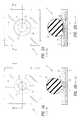
- FIG. 1Ais a top plan view of a portion of a substrate 10 having a solder-mask-defined (“SMD”) solder ball mounting pad 28 formed thereon in accordance with the prior art.
- FIG. 1Bis a cross-sectional view looking into the substrate 10 and pad 28 along the lines IB—IB in FIG. 1 A.
- the substrate 10may comprise a sheet 12 of an insulative material, such as fiberglass, polyimide tape, or ceramic, or alternatively, it may comprise a semiconductor chip or die.
- the pad 28typically comprises a layer of metal, e.g., copper, aluminum, gold, silver, nickel, tin, platinum, or a combination of the foregoing that has been laminated and/or plated on a surface of the sheet 12 , then patterned using known photolithography techniques into a central pad structure 14 , which may include one or more circuit traces 16 (shown by dotted lines) radiating outward from it. Alternatively, or in addition to the traces 16 , a plated-through hole, called a “via” 18 (shown by dotted lines), may connect the central pad 14 with the opposite surface of the sheet 12 .
- a layer of metale.g., copper, aluminum, gold, silver, nickel, tin, platinum, or a combination of the foregoing that has been laminated and/or plated on a surface of the sheet 12 , then patterned using known photolithography techniques into a central pad structure 14 , which may include one or more circuit traces 16 (shown by dotted lines) radiating out
- An insulative mask 20referred to as a passivation layer in the case of a semiconductor die, or a solder mask in the case of a BGA package, is formed over the metal layer, including the central pad 14 .
- the insulative layer 20may comprise an acrylic or a polyimide plastic, or alternatively an epoxy resin, that is silk screened or photo-deposited on the sheet 12 .
- An opening 22is formed in the insulative mask 20 to expose a central portion 28 of the central pad 14 , and a solder ball 24 (shown dotted in FIG. 1A) is attached to the pad 28 thus exposed.
- the pad 28is referred to a solder-mask-defined or SMD-type of solder ball mounting pad, as above.
- FIG. 2AA non-solder-mask-defined (“NSMD”) solder ball mounting pad 28 in accordance with the prior art is illustrated in the plan view of FIG. 2A, wherein features similar to those in the SMD pad 28 of FIG. 1A are numbered similarly.
- FIG. 2Bis a cross-sectional view looking into the substrate 10 and pad 28 along the section lines IIB—IIB in FIG. 2 A.
- the respective pads 28are very similar, the exception being the size of the opening 22 in the insulative mask 20 .
- the opening 22exposes the entire central pad 14 , along with a portion of the surface of the sheet 12 and a portion of the optional circuit trace 16 , such that the molten solder of the solder ball 24 can wet and attach to not only the entire upper surface of the central pad 14 , but also to the vertical side walls 26 of the pad and the circuit trace.
- the SMD pad 28 shown in FIGS. 1A and 1Bis the most commonly used solder ball mounting pad today. It provides good “end-of-line” (i.e., at the end of the semiconductor package fabrication line) ball 24 shear resistance because, as may be seen in FIG. 1A, the insulative mask 20 overlaps the entire peripheral edge of the central pad 14 , and hence, resists ripping of the pad from the sheet 12 when mechanical forces act on the solder ball 24 attached thereto. However, as may be seen in FIG. 2B, the insulative mask 20 covers no part of the central pad 14 portion of the NSMD pad 28 , and consequently, the latter has a relatively lower end-of-line ball 24 shear resistance.
- the SMD pad 28also affords relatively better control of the “x-y” positional tolerances of the solder ball 24 , i.e., better control of the lateral position of the solder ball 24 on the surface of the sheet 12 , than does an NSMD pad 28 having one or more circuit traces 16 leading from it, such as the one shown in FIG. 2 A.
- the x-y position of the ball 24 on the sheet 12is affected by two positional parameters: 1) the position on the sheet 12 of the centroid of the opening 22 in the insulative mask 20 , and 2) the position on the sheet of the centroid of the area of metal 28 exposed by the opening in the mask, i.e., the area wetted by the molten solder of the ball 24 when the latter is attached to the pad 28 .
- the center of gravity (“C.G.”) of the solder ball 24tends to align itself over each of the two respective centroids.
- the C.G. of the solder ball 24will be positioned approximately half way along a line extending between the two centroids.
- the shape, or “pattern,” of the area of the SMD pad 28 exposed by the circular opening 22 in the insulative mask 20is, by definition, also circular, and hence, radially symmetrical about the centroid of the exposed area of the pad.
- the centroid of the pad 28coincides with the centroid, viz., the center, of the circular opening 22 .
- the x-y tolerances on the ball 24will depend only on the x-y positional tolerances on the centroid of the opening 22 , and not on the x-y positional tolerances of the centroid of the pad 14 .
- the presence of the optional via 18will not change that result, provided the latter is also centered in the opening 22 .
- the shape of the NSMD pad 28 exposed by the opening 22 in the mask 20which includes the entire central pad 14 , as well as a portion of the circuit trace 16 , is only bilaterally symmetrical about a line passing through the center of the central pad and the circuit trace. Consequently, the centroid of the NSMD pad 28 , i.e., of the exposed area of metal, is shifted slightly toward the circuit trace 16 , and away from the centroid of the opening 22 , which is typically centered on the central pad 14 . Hence, the C.G. of the solder ball 24 will be positioned about half way between the respective centroids of the opening 22 and the NSMD pad 28
- the x-y positional tolerances on the ball 24 on an NSMD pad 28will depend not only on the x-y positional tolerances of the centroid of the opening 22 , but also the x-y positional tolerances of the centroid of the NSMD pad 28 as well.
- the presence of the optional via 18will not change that result, even if the latter is centered in the opening 22 .
- misalignment of the solder ball 24can still occur in an NSMD pad 28 if the centroid of the pad 28 is not coincident with the centroid of the opening 22 .
- a C 4 -mounted die or a C- 5 -mounted semiconductor packagecan typically have a large number, e.g., up to nine hundred, of such balls on its mounting surface, and that accordingly, these slight misalignments in the array of balls can be additive, such that in some cases, the die or package cannot be successfully mounted to an associated mounting surface.
- the prior art NSMD-type pad 28 shown in FIGS. 2A and 2Bis used less frequently today than the SMD-type of pad 28 shown in FIGS. 1A and 1B.
- the NSMD paddoes have some advantages over the SMD pad.
- the solder of the ball 24wets down and attaches to the vertical side walls 26 of the central pad 14 and the circuit trace(s) 16 , if any, to form a fillet 30 around their respective peripheries.
- This fillet structure 30helps to distribute stresses resulting from thermal aging so that the stresses do not concentrate at the interface between the pad 28 and the ball 24 .
- the interface between the pad 14 and the ball 24lacks this structure, and instead, consists of a simple interface between two planar surfaces.
- Another area of superiority of the NSMD pad 28involves the related problem of “gold embrittlement.” It is a common practice in the industry to plate solder ball mounting pads 28 with a layer of nickel, followed by a layer of gold, to improve the solderability of the pads. During the attachment of the balls 24 to the pads 28 , some of the tin in the solder combines with the gold to form a brittle “intermetallic” compound of gold and tin, which breaks away from the solder-gold interface and floats up into the molten solder ball 24 . Some of the tin in the solder also migrates through the gold to combine with the nickel and form another brittle intermetallic compound of nickel and tin.
- the joint strength between the solder ball 24 and the gold-nickel plated pad 28is good immediately after the attachment of the ball.
- some of the tin-gold intermetallic compounddiffuses back into contact with the tin-nickel intermetallic compound at the joint, and the two combine to form a hard, brittle interface that is very susceptible to stress-induced cracking.
- the fillet structure 30 in the NSMD pad 28 of FIG. 2Bacts to distribute the stresses associated with thermal aging so that the stresses do not concentrate at the interface between the ball 24 and the pad 28 , and hence, at the interface between the two intermetallic compounds. Therefore, the NSMD pad 28 of FIG. 2B exhibits a resistance to the gold embrittlement phenomenon that is superior to the SMD pad 28 of FIG. 1B, because the latter pad lacks this stress de-concentrating structure.
- the SMD pad 28has greater end-of-line ball 24 shear resistance and provides better ball x-y positional tolerances than does the NSMD pad 28 , the NSMD pad has superior thermal cycle reliability and resistance to gold embrittlement.
- This inventionprovides a method for making solder ball mounting lands, or pads, on a substrate, e.g., a PCB or a semiconductor die, that have better ball shear performance, ball thermal cycle reliability, ball attach yield, and ball positional tolerances than the solder ball mounting pads of the prior art.
- the methodincludes the provision of a sheet of material, which may be an insulator, such as fiberglass or a polyimide tape, or a layer on a semiconductor chip or die, such as silicon oxide, silicon nitride, glass, or some other insulative material, upon which it is desired to form the improved solder ball mounting pad of the invention.
- a metal layeris formed on a surface of the sheet, and the layer is patterned to define a solder ball mounting pad of the metal.
- the padis defined to include a central pad having at least two “spokes” radiating outward from it, one or more of which may comprise conventional circuit traces radiating from the pad.
- the maskmay comprise a conventional passivation layer formed over the active surface of a semiconductor die, or a solder mask formed on, e.g., a PCB or a circuit tape.
- An openingis formed in the mask that exposes the central pad and a portion of each of the spokes therethrough.
- the centroid of the opening in the maskis made to coincide with the centroid of the central pad and spoke portions exposed by the opening.
- the central pad, the spokes and the opening in the maskare arranged with respect to each other such that the exposed metal of the central pad and the spoke portions form a radially symmetrical pattern within the mask opening.
- the solder ball mounting padthus formed combines the advantages of both SMD and NSMD pad designs.
- the spokescooperate with the solder mask to hold the pad down against shear stresses, so that the shear strength of the pads, and hence, solder ball “end-of-line” reliability, is improved, relative to an NSMD pad.
- the spokesalso create fillets, i.e., regions in which the solder of the solder balls can wet around the top edges of the pad to create a complementary fillet of solder. These additional wetting areas and fillets improve the thermal cycle reliability of the ball joint as well as its resistance to gold embrittlement at the ball-pad interface, relative to an SMD pad.
- the centroid of the openingcorresponds to the centroid of the exposed metal, the solder ball will also be precisely centered in the opening when attached to the pad, thereby improving the positional tolerances of the balls, relative to an NSMD pad.
- FIG. 1Ais a top plan view of a substrate having a solder-mask-defined (“SMD”) solder ball mounting pad formed thereon in accordance with the prior art;
- SMDsolder-mask-defined
- FIG. 1Bis a cross-sectional view into the substrate and SMD mounting pad shown in FIG. 1A, as revealed by a section taken along the lines IB—IB therein;
- FIG. 2Ais a top plan view of a substrate having a non-solder-mask-defined (“NSMD”) solder ball mounting pad formed thereon in accordance with the prior art;
- NMDnon-solder-mask-defined
- FIG. 2Bis a cross-sectional view into the substrate and NSMD mounting pad shown in FIG. 1A, as revealed by a section taken along the lines IB—IB therein;
- FIG. 3Ais top plan view of a substrate having a solder ball mounting pad formed thereon in accordance with one exemplary embodiment of the present invention
- FIG. 3Bis a cross-sectional view into the substrate and novel mounting pad shown in FIG. 3A, as revealed by a section taken along the lines IIIB—IIIB therein;
- FIG. 4Ais top plan view of a substrate having a solder ball mounting pad formed thereon in accordance with another exemplary embodiment of the present invention.
- FIG. 4Bis a cross-sectional view into the substrate and novel mounting pad shown in FIG. 4A, as revealed by a section taken along the lines IVB—IVB therein.
- FIG. 3AA first exemplary embodiment of a substrate 10 having a solder ball mounting pad 28 in accordance with the present invention is illustrated in the plan view of FIG. 3A, wherein features similar to those in the SMD and NSMD pads 28 shown in FIGS. 1A-2B are numbered similarly.
- FIG. 3Bis a cross-sectional view looking into the substrate 10 and novel pad 28 along the section lines IIIB—IIIB in FIG. 3 A.
- the substrate 10comprises a sheet 12 of an insulative material, such as fiberglass, polyimide tape, or ceramic, or alternatively, it may comprise a layer on a semiconductor die, such as silicon oxide, silicon nitride, polyimide, silicon dioxide, or some other insulative material formed on the die.
- the pad 28comprises a layer of metal, e.g., copper, aluminum, gold, silver, nickel, tin, or platinum, or a combination thereof, that has been formed, e.g., by lamination or by plating, on a surface of the sheet 12 , and then patterned using photolithography techniques to define a central pad 14 therein.
- the central pad 14may include one or more circuit traces 16 (shown by dotted lines) radiating outward from it. Alternatively, or in addition to the circuit traces 16 , a via 18 (shown by dotted lines), may electrically connect the central pad 14 with the opposite surface of the sheet.
- an insulative mask 20is formed over the metal layer, and an opening 22 is formed in the insulative mask 20 that, as in the prior art NSMD pad 28 shown in FIGS. 2A and 2B above, exposes the entire central pad 14 .
- the mounting pad 28 of this inventionalso includes at least two “spokes” 32 extending outward from it in a radial direction. The spokes 32 are formed simultaneously with the central pad 14 and the circuit trace(s) 16 , if any, and from the same metal layer as the latter.
- each of these spokes 32is exposed through the opening 22 along with the central pad 14 , and an outer end portion of the spokes is covered by the insulative mask 20 .
- One or more of the spokes 32may comprise a circuit trace 16 , and for reasons of symmetry discussed below, the spokes and/or traces should have approximately the same widths.
- the pad 28may have, in addition to the at least two spokes 32 , only a via 18 connecting the central pad 14 to the opposite surface of the substrate 10 .
- the mask openingmay have a diameter of 22 mils (0.55 mm)
- the central padmay have a diameter of 14 mils (0.35 mm)
- the length and arrangement of the spokes 32must be controlled such that adjacent spokes do not short together.
- centroid of the pad 28i.e., the area of the central pad 14 and spokes 32 exposed by the circular opening 22 in the insulative mask 20 , be coincident with the centroid of the opening.
- This conditionis easily satisfied by making the “pattern” defined by the pad 28 radially symmetrical in the opening 22 in the mask 20 . It should be noted that this condition need only be satisfied within the opening 22 , and not outside of it.
- a “test” for this conditionis to determine if the pad 28 can be rotated about the centroid of the opening 22 through one or more angular positions of less than 360°, and present an identical pattern at the one or more rotated position(s).
- a “minimal” embodiment (not illustrated) of the novel mounting pad 28would include a circular central pad 14 and two elongated spokes 32 (or, e.g., one circuit trace 16 and one spoke 32 ), having equal widths, radiating outward from the pad and spaced apart from each other by 180°.
- spokes 32or, e.g., one circuit trace 16 and one spoke 32 , having equal widths, radiating outward from the pad and spaced apart from each other by 180°.
- Such a patternif rotated through 180° ( ⁇ 360°) about the centroid of the circular opening 22 , would reproduce the original pattern at the new rotated position.
- the pad 28can include, e.g., a circular central pad 14 having three spokes 32 radiating outward from it and spaced apart from each other by 120°.
- the pad 28 of the inventioncomprises a circular central pad 14 having four spokes spaced apart from each other by 90°, and eight spokes spaced apart from each other by 45°, respectively, each defining a radially symmetrical pattern within the circular opening 22 .
- the solder ball mounting pad 28 of the present inventionachieves some of the advantages, and reduces or eliminates some of the disadvantages, of both types of prior art SMD and NSMD pads 28 .
- the spokes 32are connected to the central pad 14 , and since the insulative mask 20 overlaps the end portions of each of the spokes 32 , the mask acts to prevent the spokes and central pad from being lifted from the surface of the sheet 12 by mechanical forces acting on a solder ball 24 attached to the pad 28 .
- the novel pad 28has a good end-of-line ball shear resistance, one approaching that of the prior art SMD pad 28 in FIGS. 1A and 1B.
- the central pad 14 and the spokes 32have vertical side walls 26 around their interconnected peripheries that create two or more fillets in which the solder of the ball 24 can flow and wet to create complementary fillets 30 .
- These additional wetting areas 26 and fillets 30act to distribute the stresses associated with thermal aging so that the stresses do not concentrate at the interface between the ball 24 and the pad 28 , thereby improving the thermal cycle reliability of the ball-pad solder joint, as well as its resistance to gold embrittlement, in the same manner as the NSMD pad 28 of FIGS. 2A and 2B.
- centroid of the mask opening 22is made to coincide with the centroid of the pad 28 , or alternatively, if the spokes 32 and/or circuit traces 16 are made to have approximately equal widths, and if the central pad 14 and the spokes are arranged with respect to each other and the mask opening 22 such that they form a pattern that is radially symmetrical within the opening, then x-y positional tolerances of the solder ball 24 will depend only on the positional tolerances of the opening, and the ball will be precisely centered in the opening when it is attached to the pad 28 , thereby improving the x-y positional tolerances of the ball to those of the SMD pad 28 described above.
- solder ball mounting pad design of the inventionwithout departing from its spirit and scope.
- more spoke 32 areawill give better end-of-line ball shear performance, but lower thermal cycle reliability, and vice-versa.
- a larger number of narrow spokes 32will give better overall performance than a smaller number of wider spokes.
- the central pad 14 , the spokes 32 , and the opening in the mask 20can each take a wide variety of shapes, provided only that the conditions described above are satisfied.
Landscapes
- Engineering & Computer Science (AREA)
- Microelectronics & Electronic Packaging (AREA)
- Computer Hardware Design (AREA)
- Power Engineering (AREA)
- Electric Connection Of Electric Components To Printed Circuits (AREA)
- Wire Bonding (AREA)
Abstract
Description
Claims (18)
Priority Applications (1)
| Application Number | Priority Date | Filing Date | Title |
|---|---|---|---|
| US09/591,705US6201305B1 (en) | 2000-06-09 | 2000-06-09 | Making solder ball mounting pads on substrates |
Applications Claiming Priority (1)
| Application Number | Priority Date | Filing Date | Title |
|---|---|---|---|
| US09/591,705US6201305B1 (en) | 2000-06-09 | 2000-06-09 | Making solder ball mounting pads on substrates |
Publications (1)
| Publication Number | Publication Date |
|---|---|
| US6201305B1true US6201305B1 (en) | 2001-03-13 |
Family
ID=24367555
Family Applications (1)
| Application Number | Title | Priority Date | Filing Date |
|---|---|---|---|
| US09/591,705Expired - LifetimeUS6201305B1 (en) | 2000-06-09 | 2000-06-09 | Making solder ball mounting pads on substrates |
Country Status (1)
| Country | Link |
|---|---|
| US (1) | US6201305B1 (en) |
Cited By (109)
| Publication number | Priority date | Publication date | Assignee | Title |
|---|---|---|---|---|
| US6316733B1 (en)* | 2000-08-18 | 2001-11-13 | Ga-Tek Inc. | Component for use in forming printed circuit boards |
| US6380060B1 (en)* | 2000-03-08 | 2002-04-30 | Tessera, Inc. | Off-center solder ball attach and methods therefor |
| US20020140077A1 (en)* | 1998-02-27 | 2002-10-03 | Micron Technology, Inc. | Multichip semiconductor package |
| WO2003028414A1 (en)* | 2001-09-28 | 2003-04-03 | Intel Corporation | Vented vias for via in pad technology assembly process yield improvements |
| US6552436B2 (en)* | 2000-12-08 | 2003-04-22 | Motorola, Inc. | Semiconductor device having a ball grid array and method therefor |
| US6570396B1 (en)* | 2000-11-24 | 2003-05-27 | Kulicke & Soffa Investment, Inc. | Interface structure for contacting probe beams |
| US20030201123A1 (en)* | 2002-04-30 | 2003-10-30 | Kris Kistner | Electrical connector pad assembly for printed circuit board |
| US6645791B2 (en) | 2001-04-23 | 2003-11-11 | Fairchild Semiconductor | Semiconductor die package including carrier with mask |
| US20040020972A1 (en)* | 2002-07-30 | 2004-02-05 | Yoshiyuki Miyajima | Printed circuit board and soldering structure for electronic parts thereto |
| US20040078967A1 (en)* | 1998-01-13 | 2004-04-29 | Tongbi Jiang | Z-axis electrical contact for microelectronic devices |
| US6734570B1 (en) | 2003-01-24 | 2004-05-11 | Gennum Corporation | Solder bumped substrate for a fine pitch flip-chip integrated circuit package |
| US6762503B2 (en) | 2002-08-29 | 2004-07-13 | Micron Technology, Inc. | Innovative solder ball pad structure to ease design rule, methods of fabricating same and substrates, electronic device assemblies and systems employing same |
| US20040159921A1 (en)* | 2001-12-26 | 2004-08-19 | Stephen Moxham | Methods for coupling a flowable conductive material to microelectronic substrates |
| US6787924B2 (en)* | 2001-02-13 | 2004-09-07 | Nec Corporation | Semiconductor device capable of preventing solder balls from being removed in reinforcing pad |
| US20050013978A1 (en)* | 2000-12-28 | 2005-01-20 | Canon Kabushiki Kaisha | Printed wiring board and electronic apparatus |
| US20050023683A1 (en)* | 2003-07-29 | 2005-02-03 | Myung-Kee Chung | Semiconductor package with improved ball land structure |
| US20050023679A1 (en)* | 2003-08-01 | 2005-02-03 | Advanced Semiconductor Engineering, Inc. | Substrate with reinforced contact pad structure |
| US20050098611A1 (en)* | 2003-09-25 | 2005-05-12 | Martin Reiss | Substrate for producing a soldering connection |
| DE10347622A1 (en)* | 2003-10-09 | 2005-05-25 | Infineon Technologies Ag | Substrate for making solder connection to second substrate or chip has solder pad with solderable adhesive surfaces in addition to electrical contact surface |
| US20050109532A1 (en)* | 2003-07-08 | 2005-05-26 | Hermkens Gerald A. | Method for manufacturing a sequential backplane |
| US20050109853A1 (en)* | 2003-11-20 | 2005-05-26 | Orion Electric Company Ltd. | Print-circuit board forming method and print-circuit board |
| US20050136641A1 (en)* | 2003-10-14 | 2005-06-23 | Rinne Glenn A. | Solder structures for out of plane connections and related methods |
| US20050146030A1 (en)* | 2003-12-30 | 2005-07-07 | Hiroshi Miyazaki | Solder ball pad structure |
| US20050173150A1 (en)* | 2003-02-07 | 2005-08-11 | Mitsubishi Denki Kabushiki Kaisha | Multi-layer printed board |
| US20050253231A1 (en)* | 2004-05-14 | 2005-11-17 | Advanced Semiconductor Engineering, Inc. | Semiconductor package with encapsulated passive component |
| US20050258544A1 (en)* | 2004-05-18 | 2005-11-24 | Kim Sung-Jin | Substrate for solder joint |
| US6969915B2 (en)* | 2001-01-15 | 2005-11-29 | Nec Corporation | Semiconductor device, manufacturing method and apparatus for the same |
| US20060049516A1 (en)* | 2004-09-07 | 2006-03-09 | Siliconware Precision Industries Co., Ltd. | Nickel/gold pad structure of semiconductor package and fabrication method thereof |
| US20060068180A1 (en)* | 2004-09-24 | 2006-03-30 | Denso Corporation | Printed board and manufacturing method thereof |
| US20060071333A1 (en)* | 2004-10-04 | 2006-04-06 | Osamu Miyata | Packaging substrate and semiconductor device |
| US20060105153A1 (en)* | 2004-11-12 | 2006-05-18 | Samsung Techwin Co., Ltd. | Printed circuit board and method of manufacturing the same |
| US20060131758A1 (en)* | 2004-12-22 | 2006-06-22 | Stmicroelectronics, Inc. | Anchored non-solder mask defined ball pad |
| US20060163729A1 (en)* | 2001-04-18 | 2006-07-27 | Mou-Shiung Lin | Structure and manufacturing method of a chip scale package |
| US7098408B1 (en)* | 2003-10-14 | 2006-08-29 | Cisco Technology, Inc. | Techniques for mounting an area array package to a circuit board using an improved pad layout |
| US20060220246A1 (en)* | 2004-12-07 | 2006-10-05 | Kil-Soo Kim | Bump land structure of circuit substrate for semiconductor package |
| US20060237855A1 (en)* | 2005-03-29 | 2006-10-26 | Steffen Kroehnert | Substrate for producing a soldering connection to a second substrate |
| US20060237228A1 (en)* | 2005-04-23 | 2006-10-26 | Hon Hai Precision Industry Co., Ltd. | Printed circuit board having reduced parasitic capacitance pad |
| US20060284316A1 (en)* | 2005-06-21 | 2006-12-21 | Kim Ji M | Chip size package |
| US20070102817A1 (en)* | 2002-12-17 | 2007-05-10 | Tay Cheng S | Method and apparatus for reducing electrical interconnection fatigue |
| US20070132108A1 (en)* | 2002-10-22 | 2007-06-14 | Samsung Electronics Co., Ltd. | Method for manufacturing a wafer level chip scale package |
| US7241640B1 (en)* | 2005-02-08 | 2007-07-10 | Xilinx, Inc. | Solder ball assembly for a semiconductor device and method of fabricating same |
| US20070205480A1 (en)* | 2003-09-25 | 2007-09-06 | Hiroya Kobayashi | Semiconductor Device |
| US20070262461A1 (en)* | 2006-05-09 | 2007-11-15 | Oki Electric Industry Co., Ltd. | Semiconductor device and method of producing the same |
| US20070272997A1 (en)* | 2003-09-25 | 2007-11-29 | Hiroya Kobayashi | Semiconductor Device and Method for Manufacturing the Same |
| US20070272998A1 (en)* | 2003-09-25 | 2007-11-29 | Hamamatsu Photonics K.K. | Semiconductor Device |
| US20070297151A1 (en)* | 2006-06-27 | 2007-12-27 | Mosley Larry E | Compliant conductive interconnects |
| US20080042278A1 (en)* | 2006-08-15 | 2008-02-21 | Pai-Chou Liu | Substrate structure having N-SMD ball pads |
| CN100372104C (en)* | 2004-09-07 | 2008-02-27 | 日月光半导体制造股份有限公司 | Substrate with welding pad strengthening structure |
| US20080067677A1 (en)* | 2001-03-05 | 2008-03-20 | Megica Corporation | Structure and manufacturing method of a chip scale package |
| US20080157389A1 (en)* | 2007-01-02 | 2008-07-03 | Chang-Yong Park | Semiconductor package and module printed circuit board for mounting the same |
| US7429799B1 (en) | 2005-07-27 | 2008-09-30 | Amkor Technology, Inc. | Land patterns for a semiconductor stacking structure and method therefor |
| US20080272489A1 (en)* | 2007-05-04 | 2008-11-06 | Powertech Technology Inc. | Package substrate and its solder pad |
| US20090184419A1 (en)* | 2005-05-16 | 2009-07-23 | Stats Chippac, Ltd. | Flip Chip Interconnect Solder Mask |
| US20090189298A1 (en)* | 2008-01-28 | 2009-07-30 | Fu-Chung Wu | Bonding pad structure and debug method thereof |
| US20090206493A1 (en)* | 2003-11-08 | 2009-08-20 | Stats Chippac, Ltd. | Flip Chip Interconnection Pad Layout |
| US20090250812A1 (en)* | 2005-12-22 | 2009-10-08 | Shinko Electric Industries Co., Ltd. | Flip-chip mounting substrate and flip-chip mounting method |
| US20100007019A1 (en)* | 2008-04-03 | 2010-01-14 | Stats Chippac, Ltd. | Semiconductor Device and Method of Forming Composite Bump-on-Lead Interconnection |
| US20100065966A1 (en)* | 2006-12-14 | 2010-03-18 | Stats Chippac, Ltd. | Solder Joint Flip Chip Interconnection |
| US20100099222A1 (en)* | 2006-12-14 | 2010-04-22 | Stats Chippac, Ltd. | Solder Joint Flip Chip Interconnection Having Relief Structure |
| US20100117230A1 (en)* | 2008-04-03 | 2010-05-13 | Stats Chippac, Ltd. | Flip Chip Interconnection Structure Having Void-Free Fine Pitch and Method Thereof |
| US20100164097A1 (en)* | 2008-12-31 | 2010-07-01 | Stats Chippac, Ltd. | Semiconductor Device and Method of Confining Conductive Bump Material During Reflow with Solder Mask Patch |
| US20100178735A1 (en)* | 2006-09-22 | 2010-07-15 | Stats Chippac, Inc. | Fusible I/O Interconnection Systems and Methods for Flip-Chip Packaging Involving Substrate-Mounted Stud Bumps |
| US20100193947A1 (en)* | 2005-03-25 | 2010-08-05 | Stats Chippac, Ltd. | Flip Chip Interconnection Having Narrow Interconnection Sites on the Substrate |
| US20100237500A1 (en)* | 2009-03-20 | 2010-09-23 | Stats Chippac, Ltd. | Semiconductor Substrate and Method of Forming Conformal Solder Wet-Enhancement Layer on Bump-on-Lead Site |
| US20100244245A1 (en)* | 2008-03-25 | 2010-09-30 | Stats Chippac, Ltd. | Filp Chip Interconnection Structure with Bump on Partial Pad and Method Thereof |
| US20110074024A1 (en)* | 2003-11-10 | 2011-03-31 | Stats Chippac, Ltd. | Semiconductor Device and Method of Forming Bump-on-Lead Interconnection |
| US20110074022A1 (en)* | 2000-03-10 | 2011-03-31 | Stats Chippac, Ltd. | Semiconductor Device and Method of Forming Flipchip Interconnect Structure |
| US20110074026A1 (en)* | 2008-03-19 | 2011-03-31 | Stats Chippac, Ltd. | Semiconductor Device and Method of Forming Insulating Layer on Conductive Traces for Electrical Isolation in Fine Pitch Bonding |
| US20110074047A1 (en)* | 2003-11-08 | 2011-03-31 | Stats Chippac, Ltd. | Semiconductor Device and Method of Forming Pad Layout for Flipchip Semiconductor Die |
| US20110076809A1 (en)* | 2005-05-16 | 2011-03-31 | Stats Chippac, Ltd. | Semiconductor Device and Method of Forming Narrow Interconnect Sites on Substrate with Elongated Mask Openings |
| US20110084386A1 (en)* | 2003-11-10 | 2011-04-14 | Stats Chippac, Ltd. | Semiconductor Device and Method of Self-Confinement of Conductive Bump Material During Reflow Without Solder Mask |
| US20110121464A1 (en)* | 2009-11-24 | 2011-05-26 | Stats Chippac, Ltd. | Semiconductor Device and Method of Forming Electrical Interconnect with Stress Relief Void |
| US20110121452A1 (en)* | 2008-09-10 | 2011-05-26 | Stats Chippac, Ltd. | Semiconductor Device Having Vertically Offset Bond on Trace Interconnects on Recessed and Raised Bond Fingers |
| US20110133334A1 (en)* | 2008-12-31 | 2011-06-09 | Stats Chippac, Ltd. | Semiconductor Device and Method of Confining Conductive Bump Material with Solder Mask Patch |
| US20110215468A1 (en)* | 2003-11-10 | 2011-09-08 | Stats Chippac, Ltd. | Bump-on-Lead Flip Chip Interconnection |
| US20120073867A1 (en)* | 2008-05-23 | 2012-03-29 | Unimicron Technology Corp. | Circuit structure |
| CN101996974B (en)* | 2009-08-28 | 2012-11-28 | 广达电脑股份有限公司 | Ball Grid Array Printed Circuit Board, Its Packaging Structure and Process |
| US8409978B2 (en) | 2010-06-24 | 2013-04-02 | Stats Chippac, Ltd. | Semiconductor device and method of forming vertically offset bond on trace interconnect structure on leadframe |
| JP2013069390A (en)* | 2011-09-26 | 2013-04-18 | Dainippon Printing Co Ltd | Suspension substrate, suspension, suspension with head, and hard disk drive |
| US8435834B2 (en) | 2010-09-13 | 2013-05-07 | Stats Chippac, Ltd. | Semiconductor device and method of forming bond-on-lead interconnection for mounting semiconductor die in FO-WLCSP |
| US20130153282A1 (en)* | 2011-12-20 | 2013-06-20 | Msi Computer(Shenzhen)Co., Ltd. | Printed circuit board |
| US8492197B2 (en) | 2010-08-17 | 2013-07-23 | Stats Chippac, Ltd. | Semiconductor device and method of forming vertically offset conductive pillars over first substrate aligned to vertically offset BOT interconnect sites formed over second substrate |
| USRE44500E1 (en) | 2003-11-10 | 2013-09-17 | Stats Chippac, Ltd. | Semiconductor device and method of forming composite bump-on-lead interconnection |
| US20130270705A1 (en)* | 2012-04-11 | 2013-10-17 | Taiwan Semiconductor Manufacturing Company, Ltd. | Semiconductor Device Packages and Methods |
| US8563418B2 (en) | 2010-03-09 | 2013-10-22 | Stats Chippac, Ltd. | Semiconductor device and method of forming vertically offset bond on trace interconnects on different height traces |
| USRE44562E1 (en) | 2003-11-10 | 2013-10-29 | Stats Chippac, Ltd. | Solder joint flip chip interconnection having relief structure |
| USRE44579E1 (en) | 2003-11-10 | 2013-11-05 | Stats Chippac, Ltd. | Semiconductor device and method of self-confinement of conductive bump material during reflow without solder mask |
| USRE44608E1 (en) | 2003-11-10 | 2013-11-26 | Stats Chippac, Ltd. | Solder joint flip chip interconnection |
| US20130323526A1 (en)* | 2012-05-29 | 2013-12-05 | Essence Solar Solutions Ltd. | Self aligning soldering |
| CN103458613A (en)* | 2012-05-31 | 2013-12-18 | 佳能株式会社 | Circuit board and image forming apparatus |
| US8697490B2 (en) | 2000-03-10 | 2014-04-15 | Stats Chippac, Ltd. | Flip chip interconnection structure |
| US8704369B1 (en)* | 2008-06-23 | 2014-04-22 | Amkor Technology, Inc. | Flip chip bump structure and fabrication method |
| US8841779B2 (en) | 2005-03-25 | 2014-09-23 | Stats Chippac, Ltd. | Semiconductor device and method of forming high routing density BOL BONL and BONP interconnect sites on substrate |
| CN104955268A (en)* | 2014-03-26 | 2015-09-30 | 鸿富锦精密工业(武汉)有限公司 | Circuit board |
| US20150287685A1 (en)* | 2014-04-02 | 2015-10-08 | Freescale Semiconductor, Inc. | Solder Pad for Semiconductor Device Package |
| US9281286B1 (en)* | 2014-08-27 | 2016-03-08 | Freescale Semiconductor Inc. | Microelectronic packages having texturized solder pads and methods for the fabrication thereof |
| US9345148B2 (en) | 2008-03-25 | 2016-05-17 | Stats Chippac, Ltd. | Semiconductor device and method of forming flipchip interconnection structure with bump on partial pad |
| US20160172321A1 (en)* | 2014-12-16 | 2016-06-16 | Nantong Fujitsu Microelectronics Co., Ltd. | Method and structure for wafer-level packaging |
| US9425174B1 (en)* | 2014-11-18 | 2016-08-23 | Altera Corporation | Integrated circuit package with solderless interconnection structure |
| TWI582871B (en)* | 2014-10-13 | 2017-05-11 | 艾馬克科技公司 | A patterned pad to create a virtual solder mask for wafer-level chip-scale packages |
| US9847309B2 (en) | 2006-09-22 | 2017-12-19 | STATS ChipPAC Pte. Ltd. | Semiconductor device and method of forming vertical interconnect structure between semiconductor die and substrate |
| US20190067199A1 (en)* | 2017-08-22 | 2019-02-28 | Shinko Electric Industries Co., Ltd. | Wiring board and electronic device |
| USRE47600E1 (en) | 2003-11-10 | 2019-09-10 | STATS ChipPAC Pte. Ltd. | Semiconductor device and method of forming electrical interconnect with stress relief void |
| US10825789B1 (en) | 2019-08-26 | 2020-11-03 | Nxp B.V. | Underbump metallization dimension variation with improved reliability |
| JP2021007163A (en)* | 2020-09-28 | 2021-01-21 | キヤノン株式会社 | Printed circuit boards and electronic devices |
| US11355429B2 (en)* | 2020-01-28 | 2022-06-07 | Infineon Technologies Ag | Electrical interconnect structure with radial spokes for improved solder void control |
| US20230260926A1 (en)* | 2022-02-16 | 2023-08-17 | Samsung Electronics Co., Ltd. | Semiconductor packages having fixing members |
| US20230378044A1 (en)* | 2022-05-19 | 2023-11-23 | Chipbond Technology Corporation | Flip-chip bonding structure and substrate thereof |
| US20240332230A1 (en)* | 2021-08-30 | 2024-10-03 | Taiwan Semiconductor Manufacturing Company, Ltd. | Semiconductor device |
Citations (2)
| Publication number | Priority date | Publication date | Assignee | Title |
|---|---|---|---|---|
| US5327013A (en)* | 1992-04-30 | 1994-07-05 | Motorola, Inc. | Solder bumping of integrated circuit die |
| US5977632A (en)* | 1998-02-02 | 1999-11-02 | Motorola, Inc. | Flip chip bump structure and method of making |
- 2000
- 2000-06-09USUS09/591,705patent/US6201305B1/ennot_activeExpired - Lifetime
Patent Citations (2)
| Publication number | Priority date | Publication date | Assignee | Title |
|---|---|---|---|---|
| US5327013A (en)* | 1992-04-30 | 1994-07-05 | Motorola, Inc. | Solder bumping of integrated circuit die |
| US5977632A (en)* | 1998-02-02 | 1999-11-02 | Motorola, Inc. | Flip chip bump structure and method of making |
Cited By (242)
| Publication number | Priority date | Publication date | Assignee | Title |
|---|---|---|---|---|
| US7213331B2 (en)* | 1998-01-13 | 2007-05-08 | Micron Technology, Inc. | Method for forming stencil |
| US20040078967A1 (en)* | 1998-01-13 | 2004-04-29 | Tongbi Jiang | Z-axis electrical contact for microelectronic devices |
| US6906409B2 (en) | 1998-02-27 | 2005-06-14 | Micron Technology, Inc. | Multichip semiconductor package |
| US20020140077A1 (en)* | 1998-02-27 | 2002-10-03 | Micron Technology, Inc. | Multichip semiconductor package |
| US20050212143A1 (en)* | 1998-02-27 | 2005-09-29 | Micron Technology, Inc. | Multichip semiconductor package |
| US20020117761A1 (en)* | 2000-03-08 | 2002-08-29 | Wael Zohni | Off-center solder ball attach assembly |
| US6870267B2 (en) | 2000-03-08 | 2005-03-22 | Tessera, Inc. | Off-center solder ball attach assembly |
| US6380060B1 (en)* | 2000-03-08 | 2002-04-30 | Tessera, Inc. | Off-center solder ball attach and methods therefor |
| US10388626B2 (en) | 2000-03-10 | 2019-08-20 | STATS ChipPAC Pte. Ltd. | Semiconductor device and method of forming flipchip interconnect structure |
| US20110074022A1 (en)* | 2000-03-10 | 2011-03-31 | Stats Chippac, Ltd. | Semiconductor Device and Method of Forming Flipchip Interconnect Structure |
| US8697490B2 (en) | 2000-03-10 | 2014-04-15 | Stats Chippac, Ltd. | Flip chip interconnection structure |
| US6316733B1 (en)* | 2000-08-18 | 2001-11-13 | Ga-Tek Inc. | Component for use in forming printed circuit boards |
| US6570396B1 (en)* | 2000-11-24 | 2003-05-27 | Kulicke & Soffa Investment, Inc. | Interface structure for contacting probe beams |
| US6552436B2 (en)* | 2000-12-08 | 2003-04-22 | Motorola, Inc. | Semiconductor device having a ball grid array and method therefor |
| US20030102535A1 (en)* | 2000-12-08 | 2003-06-05 | Burnette Terry E. | Semiconductor device having a ball grid array and method therefor |
| US20050013978A1 (en)* | 2000-12-28 | 2005-01-20 | Canon Kabushiki Kaisha | Printed wiring board and electronic apparatus |
| US20100015796A1 (en)* | 2001-01-15 | 2010-01-21 | Nec Corporation | Semiconductor device, manufacturing method and apparatus for the same |
| US7611041B2 (en) | 2001-01-15 | 2009-11-03 | Nec Corporation | Semiconductor device, manufacturing method and apparatus for the same |
| US20050279812A1 (en)* | 2001-01-15 | 2005-12-22 | Nec Corporation | Semiconductor device, manufacturing method and apparatus for the same |
| US6969915B2 (en)* | 2001-01-15 | 2005-11-29 | Nec Corporation | Semiconductor device, manufacturing method and apparatus for the same |
| US20070295786A1 (en)* | 2001-01-15 | 2007-12-27 | Nec Corporation | Semiconductor device, manufacturing method and apparatus for the same |
| US7793818B2 (en) | 2001-01-15 | 2010-09-14 | Nec Corporation | Semiconductor device, manufacturing method and apparatus for the same |
| US7282432B2 (en) | 2001-01-15 | 2007-10-16 | Nec Corporation | Semiconductor device, manufacturing method and apparatus for the same |
| US6787924B2 (en)* | 2001-02-13 | 2004-09-07 | Nec Corporation | Semiconductor device capable of preventing solder balls from being removed in reinforcing pad |
| US20080067677A1 (en)* | 2001-03-05 | 2008-03-20 | Megica Corporation | Structure and manufacturing method of a chip scale package |
| US20090267213A1 (en)* | 2001-03-05 | 2009-10-29 | Megica Corporation | Structure and manufacturing method of a chip scale package with low fabrication cost, fine pitch and high reliability solder bump |
| US7902679B2 (en) | 2001-03-05 | 2011-03-08 | Megica Corporation | Structure and manufacturing method of a chip scale package with low fabrication cost, fine pitch and high reliability solder bump |
| US8158508B2 (en) | 2001-03-05 | 2012-04-17 | Megica Corporation | Structure and manufacturing method of a chip scale package |
| US20060163729A1 (en)* | 2001-04-18 | 2006-07-27 | Mou-Shiung Lin | Structure and manufacturing method of a chip scale package |
| US7157799B2 (en) | 2001-04-23 | 2007-01-02 | Fairchild Semiconductor Corporation | Semiconductor die package including carrier with mask and semiconductor die |
| US6645791B2 (en) | 2001-04-23 | 2003-11-11 | Fairchild Semiconductor | Semiconductor die package including carrier with mask |
| CN100433949C (en)* | 2001-09-28 | 2008-11-12 | 英特尔公司 | Vented vias for via in pad technology assembly process yield improvements |
| WO2003028414A1 (en)* | 2001-09-28 | 2003-04-03 | Intel Corporation | Vented vias for via in pad technology assembly process yield improvements |
| US20050242437A1 (en)* | 2001-12-26 | 2005-11-03 | Micron Technology, Inc. | Method and apparatus for supporting microelectronic substrates |
| US6995026B2 (en) | 2001-12-26 | 2006-02-07 | Micron Technology, Inc. | Methods for coupling a flowable conductive material to microelectronic substrates |
| US20040159921A1 (en)* | 2001-12-26 | 2004-08-19 | Stephen Moxham | Methods for coupling a flowable conductive material to microelectronic substrates |
| US6870276B1 (en)* | 2001-12-26 | 2005-03-22 | Micron Technology, Inc. | Apparatus for supporting microelectronic substrates |
| US20040159946A1 (en)* | 2001-12-26 | 2004-08-19 | Stephen Moxham | Microelectronic assemblies, electronic devices, and apparatuses for supporting microelectronic substrates |
| US6936916B2 (en) | 2001-12-26 | 2005-08-30 | Micron Technology, Inc. | Microelectronic assemblies and electronic devices including connection structures with multiple elongated members |
| US20030201123A1 (en)* | 2002-04-30 | 2003-10-30 | Kris Kistner | Electrical connector pad assembly for printed circuit board |
| US6828513B2 (en)* | 2002-04-30 | 2004-12-07 | Texas Instruments Incorporated | Electrical connector pad assembly for printed circuit board |
| US20040020972A1 (en)* | 2002-07-30 | 2004-02-05 | Yoshiyuki Miyajima | Printed circuit board and soldering structure for electronic parts thereto |
| US6853091B2 (en)* | 2002-07-30 | 2005-02-08 | Orion Electric Co., Ltd. | Printed circuit board and soldering structure for electronic parts thereto |
| US20040173915A1 (en)* | 2002-08-29 | 2004-09-09 | Lee Teck Kheng | Innovative solder ball pad structure to ease design rule, methods of fabricating same and substrates, electronic device assemblies and systems employing same |
| US6762503B2 (en) | 2002-08-29 | 2004-07-13 | Micron Technology, Inc. | Innovative solder ball pad structure to ease design rule, methods of fabricating same and substrates, electronic device assemblies and systems employing same |
| US6940179B2 (en)* | 2002-08-29 | 2005-09-06 | Micron Technology, Inc. | Innovative solder ball pad structure to ease design rule, methods of fabricating same and substrates, electronic device assemblies and systems employing same |
| US20070132108A1 (en)* | 2002-10-22 | 2007-06-14 | Samsung Electronics Co., Ltd. | Method for manufacturing a wafer level chip scale package |
| US7642660B2 (en)* | 2002-12-17 | 2010-01-05 | Cheng Siew Tay | Method and apparatus for reducing electrical interconnection fatigue |
| US20070102817A1 (en)* | 2002-12-17 | 2007-05-10 | Tay Cheng S | Method and apparatus for reducing electrical interconnection fatigue |
| US6734570B1 (en) | 2003-01-24 | 2004-05-11 | Gennum Corporation | Solder bumped substrate for a fine pitch flip-chip integrated circuit package |
| US6969808B2 (en)* | 2003-02-07 | 2005-11-29 | Mitsubishi Denki Kabushiki Kaisha | Multi-layer printed board |
| US20050173150A1 (en)* | 2003-02-07 | 2005-08-11 | Mitsubishi Denki Kabushiki Kaisha | Multi-layer printed board |
| US20050109532A1 (en)* | 2003-07-08 | 2005-05-26 | Hermkens Gerald A. | Method for manufacturing a sequential backplane |
| US7172805B2 (en)* | 2003-07-08 | 2007-02-06 | Viasytems Group, Inc. | Method for manufacturing a sequential backplane |
| US20060278430A1 (en)* | 2003-07-08 | 2006-12-14 | Viasystems Group, Inc. | Method for manufacturing a midplane |
| US20050023683A1 (en)* | 2003-07-29 | 2005-02-03 | Myung-Kee Chung | Semiconductor package with improved ball land structure |
| US7064435B2 (en)* | 2003-07-29 | 2006-06-20 | Samsung Electronics Co., Ltd. | Semiconductor package with improved ball land structure |
| US7005750B2 (en)* | 2003-08-01 | 2006-02-28 | Advanced Semiconductor Engineering, Inc. | Substrate with reinforced contact pad structure |
| US20050023679A1 (en)* | 2003-08-01 | 2005-02-03 | Advanced Semiconductor Engineering, Inc. | Substrate with reinforced contact pad structure |
| US7271484B2 (en)* | 2003-09-25 | 2007-09-18 | Infineon Technologies Ag | Substrate for producing a soldering connection |
| US20070205480A1 (en)* | 2003-09-25 | 2007-09-06 | Hiroya Kobayashi | Semiconductor Device |
| US20070272998A1 (en)* | 2003-09-25 | 2007-11-29 | Hamamatsu Photonics K.K. | Semiconductor Device |
| US20070272997A1 (en)* | 2003-09-25 | 2007-11-29 | Hiroya Kobayashi | Semiconductor Device and Method for Manufacturing the Same |
| US7696595B2 (en) | 2003-09-25 | 2010-04-13 | Hamamatsu Photonics K.K. | Semiconductor device and method for manufacturing the same |
| EP1672694A4 (en)* | 2003-09-25 | 2008-10-01 | Hamamatsu Photonics Kk | SEMICONDUCTOR COMPONENT |
| US20050098611A1 (en)* | 2003-09-25 | 2005-05-12 | Martin Reiss | Substrate for producing a soldering connection |
| US7605455B2 (en) | 2003-09-25 | 2009-10-20 | Hamamatsu Photonics K.K. | Semiconductor device |
| US7612442B2 (en) | 2003-09-25 | 2009-11-03 | Hamamatsu Photonics K.K. | Semiconductor device |
| DE10347622B4 (en)* | 2003-10-09 | 2006-09-07 | Infineon Technologies Ag | Substrate with solder pad for making a solder joint |
| DE10347622A1 (en)* | 2003-10-09 | 2005-05-25 | Infineon Technologies Ag | Substrate for making solder connection to second substrate or chip has solder pad with solderable adhesive surfaces in addition to electrical contact surface |
| US7049216B2 (en) | 2003-10-14 | 2006-05-23 | Unitive International Limited | Methods of providing solder structures for out plane connections |
| US20050136641A1 (en)* | 2003-10-14 | 2005-06-23 | Rinne Glenn A. | Solder structures for out of plane connections and related methods |
| US7098408B1 (en)* | 2003-10-14 | 2006-08-29 | Cisco Technology, Inc. | Techniques for mounting an area array package to a circuit board using an improved pad layout |
| US7659621B2 (en) | 2003-10-14 | 2010-02-09 | Unitive International Limited | Solder structures for out of plane connections |
| WO2005039261A3 (en)* | 2003-10-14 | 2005-08-25 | Unitive Int Ltd | Solder structures for out of plane connections and related methods |
| US20060138675A1 (en)* | 2003-10-14 | 2006-06-29 | Rinne Glenn A | Solder structures for out of plane connections |
| US20110074047A1 (en)* | 2003-11-08 | 2011-03-31 | Stats Chippac, Ltd. | Semiconductor Device and Method of Forming Pad Layout for Flipchip Semiconductor Die |
| US20090206493A1 (en)* | 2003-11-08 | 2009-08-20 | Stats Chippac, Ltd. | Flip Chip Interconnection Pad Layout |
| US8129837B2 (en) | 2003-11-08 | 2012-03-06 | Stats Chippac, Ltd. | Flip chip interconnection pad layout |
| US9780057B2 (en) | 2003-11-08 | 2017-10-03 | STATS ChipPAC Pte. Ltd. | Semiconductor device and method of forming pad layout for flipchip semiconductor die |
| US20110084386A1 (en)* | 2003-11-10 | 2011-04-14 | Stats Chippac, Ltd. | Semiconductor Device and Method of Self-Confinement of Conductive Bump Material During Reflow Without Solder Mask |
| US9064858B2 (en) | 2003-11-10 | 2015-06-23 | Stats Chippac, Ltd. | Semiconductor device and method of forming bump-on-lead interconnection |
| US20110074024A1 (en)* | 2003-11-10 | 2011-03-31 | Stats Chippac, Ltd. | Semiconductor Device and Method of Forming Bump-on-Lead Interconnection |
| USRE44608E1 (en) | 2003-11-10 | 2013-11-26 | Stats Chippac, Ltd. | Solder joint flip chip interconnection |
| USRE44761E1 (en) | 2003-11-10 | 2014-02-11 | Stats Chippac, Ltd. | Solder joint flip chip interconnection having relief structure |
| USRE44579E1 (en) | 2003-11-10 | 2013-11-05 | Stats Chippac, Ltd. | Semiconductor device and method of self-confinement of conductive bump material during reflow without solder mask |
| US8574959B2 (en) | 2003-11-10 | 2013-11-05 | Stats Chippac, Ltd. | Semiconductor device and method of forming bump-on-lead interconnection |
| USRE47600E1 (en) | 2003-11-10 | 2019-09-10 | STATS ChipPAC Pte. Ltd. | Semiconductor device and method of forming electrical interconnect with stress relief void |
| USRE44562E1 (en) | 2003-11-10 | 2013-10-29 | Stats Chippac, Ltd. | Solder joint flip chip interconnection having relief structure |
| US8759972B2 (en) | 2003-11-10 | 2014-06-24 | Stats Chippac, Ltd. | Semiconductor device and method of forming composite bump-on-lead interconnection |
| US8810029B2 (en) | 2003-11-10 | 2014-08-19 | Stats Chippac, Ltd. | Solder joint flip chip interconnection |
| US9899286B2 (en) | 2003-11-10 | 2018-02-20 | STATS ChipPAC Pte. Ltd. | Semiconductor device and method of self-confinement of conductive bump material during reflow without solder mask |
| US8558378B2 (en) | 2003-11-10 | 2013-10-15 | Stats Chippac, Ltd. | Bump-on-lead flip chip interconnection |
| USRE44524E1 (en) | 2003-11-10 | 2013-10-08 | Stats Chippac, Ltd. | Bump-on-lead flip chip interconnection |
| USRE44500E1 (en) | 2003-11-10 | 2013-09-17 | Stats Chippac, Ltd. | Semiconductor device and method of forming composite bump-on-lead interconnection |
| USRE44431E1 (en) | 2003-11-10 | 2013-08-13 | Stats Chippac, Ltd. | Bump-on-lead flip chip interconnection |
| USRE44377E1 (en) | 2003-11-10 | 2013-07-16 | Stats Chippac, Ltd. | Bump-on-lead flip chip interconnection |
| USRE44355E1 (en) | 2003-11-10 | 2013-07-09 | Stats Chippac, Ltd. | Method of forming a bump-on-lead flip chip interconnection having higher escape routing density |
| US9029196B2 (en) | 2003-11-10 | 2015-05-12 | Stats Chippac, Ltd. | Semiconductor device and method of self-confinement of conductive bump material during reflow without solder mask |
| US9922915B2 (en) | 2003-11-10 | 2018-03-20 | STATS ChipPAC Pte. Ltd. | Bump-on-lead flip chip interconnection |
| US9865556B2 (en) | 2003-11-10 | 2018-01-09 | STATS ChipPAC Pte Ltd. | Semiconductor device and method of self-confinement of conductive bump material during reflow without solder mask |
| US9219045B2 (en) | 2003-11-10 | 2015-12-22 | Stats Chippac, Ltd. | Semiconductor device and method of self-confinement of conductive bump material during reflow without solder mask |
| US20110215468A1 (en)* | 2003-11-10 | 2011-09-08 | Stats Chippac, Ltd. | Bump-on-Lead Flip Chip Interconnection |
| US9373573B2 (en) | 2003-11-10 | 2016-06-21 | STATS ChipPAC Pte. Ltd. | Solder joint flip chip interconnection |
| US9379084B2 (en) | 2003-11-10 | 2016-06-28 | STATS ChipPAC Pte. Ltd. | Semiconductor device and method of self-confinement of conductive bump material during reflow without solder mask |
| US9385101B2 (en) | 2003-11-10 | 2016-07-05 | STATS ChipPAC Pte. Ltd. | Semiconductor device and method of forming bump-on-lead interconnection |
| US8188598B2 (en) | 2003-11-10 | 2012-05-29 | Stats Chippac, Ltd. | Bump-on-lead flip chip interconnection |
| US9773685B2 (en) | 2003-11-10 | 2017-09-26 | STATS ChipPAC Pte. Ltd. | Solder joint flip chip interconnection having relief structure |
| US20050109853A1 (en)* | 2003-11-20 | 2005-05-26 | Orion Electric Company Ltd. | Print-circuit board forming method and print-circuit board |
| US20050146030A1 (en)* | 2003-12-30 | 2005-07-07 | Hiroshi Miyazaki | Solder ball pad structure |
| US7294929B2 (en) | 2003-12-30 | 2007-11-13 | Texas Instruments Incorporated | Solder ball pad structure |
| US20080026559A1 (en)* | 2003-12-30 | 2008-01-31 | Texas Instruments Incorporated | Solder Ball Pad Structure |
| US20050253231A1 (en)* | 2004-05-14 | 2005-11-17 | Advanced Semiconductor Engineering, Inc. | Semiconductor package with encapsulated passive component |
| US7268437B2 (en)* | 2004-05-14 | 2007-09-11 | Advanced Semiconductor Engineering, Inc. | Semiconductor package with encapsulated passive component |
| US20050258544A1 (en)* | 2004-05-18 | 2005-11-24 | Kim Sung-Jin | Substrate for solder joint |
| US7224073B2 (en) | 2004-05-18 | 2007-05-29 | Ultratera Corporation | Substrate for solder joint |
| CN100372104C (en)* | 2004-09-07 | 2008-02-27 | 日月光半导体制造股份有限公司 | Substrate with welding pad strengthening structure |
| US20060049516A1 (en)* | 2004-09-07 | 2006-03-09 | Siliconware Precision Industries Co., Ltd. | Nickel/gold pad structure of semiconductor package and fabrication method thereof |
| US20060068180A1 (en)* | 2004-09-24 | 2006-03-30 | Denso Corporation | Printed board and manufacturing method thereof |
| US7323238B2 (en)* | 2004-09-24 | 2008-01-29 | Denso Corporation | Printed circuit board having colored outer layer |
| US20060071333A1 (en)* | 2004-10-04 | 2006-04-06 | Osamu Miyata | Packaging substrate and semiconductor device |
| US7436063B2 (en)* | 2004-10-04 | 2008-10-14 | Rohm Co., Ltd. | Packaging substrate and semiconductor device |
| US20060105153A1 (en)* | 2004-11-12 | 2006-05-18 | Samsung Techwin Co., Ltd. | Printed circuit board and method of manufacturing the same |
| US7811626B2 (en) | 2004-11-12 | 2010-10-12 | Samsung Techwin Co., Ltd. | Printed circuit board and method of manufacturing the same |
| US7470461B2 (en)* | 2004-11-12 | 2008-12-30 | Samsung Techwin Co., Ltd. | Printed circuit board and method of manufacturing the same |
| US20090087547A1 (en)* | 2004-11-12 | 2009-04-02 | Samsung Techwin Co., Ltd. | Printed circuit board and method of manufacturing the same |
| US20060220246A1 (en)* | 2004-12-07 | 2006-10-05 | Kil-Soo Kim | Bump land structure of circuit substrate for semiconductor package |
| US20060131758A1 (en)* | 2004-12-22 | 2006-06-22 | Stmicroelectronics, Inc. | Anchored non-solder mask defined ball pad |
| US20070246817A1 (en)* | 2005-02-08 | 2007-10-25 | Xilinx, Inc. | Solder ball assembly for a semiconductor device and method of fabricating same |
| US7545028B2 (en)* | 2005-02-08 | 2009-06-09 | Xilinx, Inc. | Solder ball assembly for a semiconductor device and method of fabricating same |
| US7241640B1 (en)* | 2005-02-08 | 2007-07-10 | Xilinx, Inc. | Solder ball assembly for a semiconductor device and method of fabricating same |
| US8841779B2 (en) | 2005-03-25 | 2014-09-23 | Stats Chippac, Ltd. | Semiconductor device and method of forming high routing density BOL BONL and BONP interconnect sites on substrate |
| US20100193947A1 (en)* | 2005-03-25 | 2010-08-05 | Stats Chippac, Ltd. | Flip Chip Interconnection Having Narrow Interconnection Sites on the Substrate |
| US9159665B2 (en) | 2005-03-25 | 2015-10-13 | Stats Chippac, Ltd. | Flip chip interconnection having narrow interconnection sites on the substrate |
| US10580749B2 (en) | 2005-03-25 | 2020-03-03 | STATS ChipPAC Pte. Ltd. | Semiconductor device and method of forming high routing density interconnect sites on substrate |
| US8318537B2 (en) | 2005-03-25 | 2012-11-27 | Stats Chippac, Ltd. | Flip chip interconnection having narrow interconnection sites on the substrate |
| US20060237855A1 (en)* | 2005-03-29 | 2006-10-26 | Steffen Kroehnert | Substrate for producing a soldering connection to a second substrate |
| DE102005014665A1 (en)* | 2005-03-29 | 2006-11-02 | Infineon Technologies Ag | Substrate for producing a solder joint with a second substrate |
| CN100518435C (en)* | 2005-04-23 | 2009-07-22 | 鸿富锦精密工业(深圳)有限公司 | Printed circuit board with improved solder pads |
| US20060237228A1 (en)* | 2005-04-23 | 2006-10-26 | Hon Hai Precision Industry Co., Ltd. | Printed circuit board having reduced parasitic capacitance pad |
| US20090184419A1 (en)* | 2005-05-16 | 2009-07-23 | Stats Chippac, Ltd. | Flip Chip Interconnect Solder Mask |
| US9545014B2 (en) | 2005-05-16 | 2017-01-10 | STATS ChipPAC Pte. Ltd. | Flip chip interconnect solder mask |
| US9545013B2 (en) | 2005-05-16 | 2017-01-10 | STATS ChipPAC Pte. Ltd. | Flip chip interconnect solder mask |
| US8278144B2 (en) | 2005-05-16 | 2012-10-02 | Stats Chippac, Ltd. | Flip chip interconnect solder mask |
| US9258904B2 (en) | 2005-05-16 | 2016-02-09 | Stats Chippac, Ltd. | Semiconductor device and method of forming narrow interconnect sites on substrate with elongated mask openings |
| US20110076809A1 (en)* | 2005-05-16 | 2011-03-31 | Stats Chippac, Ltd. | Semiconductor Device and Method of Forming Narrow Interconnect Sites on Substrate with Elongated Mask Openings |
| US20060284316A1 (en)* | 2005-06-21 | 2006-12-21 | Kim Ji M | Chip size package |
| KR100701695B1 (en)* | 2005-06-21 | 2007-03-29 | 주식회사 하이닉스반도체 | Chip size package |
| US7429799B1 (en) | 2005-07-27 | 2008-09-30 | Amkor Technology, Inc. | Land patterns for a semiconductor stacking structure and method therefor |
| US7691745B1 (en) | 2005-07-27 | 2010-04-06 | Amkor Technology, Inc. | Land patterns for a semiconductor stacking structure and method therefor |
| US8669665B2 (en)* | 2005-12-22 | 2014-03-11 | Shinko Electric Industries Co., Ltd. | Flip-chip mounting substrate and flip-chip mounting method |
| US20090250812A1 (en)* | 2005-12-22 | 2009-10-08 | Shinko Electric Industries Co., Ltd. | Flip-chip mounting substrate and flip-chip mounting method |
| US7652380B2 (en)* | 2006-05-09 | 2010-01-26 | Oki Semiconductor Co., Ltd. | Semiconductor device and method of producing the same |
| US20070262461A1 (en)* | 2006-05-09 | 2007-11-15 | Oki Electric Industry Co., Ltd. | Semiconductor device and method of producing the same |
| US20070297151A1 (en)* | 2006-06-27 | 2007-12-27 | Mosley Larry E | Compliant conductive interconnects |
| US20080042278A1 (en)* | 2006-08-15 | 2008-02-21 | Pai-Chou Liu | Substrate structure having N-SMD ball pads |
| US7911056B2 (en)* | 2006-08-15 | 2011-03-22 | Advanced Semiconductor Engineering, Inc. | Substrate structure having N-SMD ball pads |
| US20100178735A1 (en)* | 2006-09-22 | 2010-07-15 | Stats Chippac, Inc. | Fusible I/O Interconnection Systems and Methods for Flip-Chip Packaging Involving Substrate-Mounted Stud Bumps |
| US9847309B2 (en) | 2006-09-22 | 2017-12-19 | STATS ChipPAC Pte. Ltd. | Semiconductor device and method of forming vertical interconnect structure between semiconductor die and substrate |
| US8525350B2 (en) | 2006-09-22 | 2013-09-03 | Stats Chippac, Ltd. | Fusible I/O interconnection systems and methods for flip-chip packaging involving substrate-mounted stud bumps |
| US20100176510A1 (en)* | 2006-09-22 | 2010-07-15 | Stats Chippac, Inc. | Fusible I/O Interconnection Systems and Methods for Flip-Chip Packaging Involving Substrate-Mounted Stud Bumps |
| US8193035B2 (en) | 2006-09-22 | 2012-06-05 | Stats Chippac, Ltd. | Fusible I/O interconnection systems and methods for flip-chip packaging involving substrate-mounted stud bumps |
| US20100099222A1 (en)* | 2006-12-14 | 2010-04-22 | Stats Chippac, Ltd. | Solder Joint Flip Chip Interconnection Having Relief Structure |
| US20100065966A1 (en)* | 2006-12-14 | 2010-03-18 | Stats Chippac, Ltd. | Solder Joint Flip Chip Interconnection |
| US8129841B2 (en) | 2006-12-14 | 2012-03-06 | Stats Chippac, Ltd. | Solder joint flip chip interconnection |
| US8216930B2 (en) | 2006-12-14 | 2012-07-10 | Stats Chippac, Ltd. | Solder joint flip chip interconnection having relief structure |
| US20080157389A1 (en)* | 2007-01-02 | 2008-07-03 | Chang-Yong Park | Semiconductor package and module printed circuit board for mounting the same |
| US7675176B2 (en) | 2007-01-02 | 2010-03-09 | Samsung Electronics Co., Ltd. | Semiconductor package and module printed circuit board for mounting the same |
| US20080272489A1 (en)* | 2007-05-04 | 2008-11-06 | Powertech Technology Inc. | Package substrate and its solder pad |
| US20090189298A1 (en)* | 2008-01-28 | 2009-07-30 | Fu-Chung Wu | Bonding pad structure and debug method thereof |
| US20110074026A1 (en)* | 2008-03-19 | 2011-03-31 | Stats Chippac, Ltd. | Semiconductor Device and Method of Forming Insulating Layer on Conductive Traces for Electrical Isolation in Fine Pitch Bonding |
| US8349721B2 (en) | 2008-03-19 | 2013-01-08 | Stats Chippac, Ltd. | Semiconductor device and method of forming insulating layer on conductive traces for electrical isolation in fine pitch bonding |
| US9418913B2 (en) | 2008-03-19 | 2016-08-16 | STATS ChipPAC Pte. Ltd. | Semiconductor device and method of forming insulating layer on conductive traces for electrical isolation in fine pitch bonding |
| US20100244245A1 (en)* | 2008-03-25 | 2010-09-30 | Stats Chippac, Ltd. | Filp Chip Interconnection Structure with Bump on Partial Pad and Method Thereof |
| US9125332B2 (en)* | 2008-03-25 | 2015-09-01 | Stats Chippac, Ltd. | Filp chip interconnection structure with bump on partial pad and method thereof |
| US9345148B2 (en) | 2008-03-25 | 2016-05-17 | Stats Chippac, Ltd. | Semiconductor device and method of forming flipchip interconnection structure with bump on partial pad |
| US20100007019A1 (en)* | 2008-04-03 | 2010-01-14 | Stats Chippac, Ltd. | Semiconductor Device and Method of Forming Composite Bump-on-Lead Interconnection |
| US20100117230A1 (en)* | 2008-04-03 | 2010-05-13 | Stats Chippac, Ltd. | Flip Chip Interconnection Structure Having Void-Free Fine Pitch and Method Thereof |
| US8076232B2 (en) | 2008-04-03 | 2011-12-13 | Stats Chippac, Ltd. | Semiconductor device and method of forming composite bump-on-lead interconnection |
| US20120073867A1 (en)* | 2008-05-23 | 2012-03-29 | Unimicron Technology Corp. | Circuit structure |
| US8704369B1 (en)* | 2008-06-23 | 2014-04-22 | Amkor Technology, Inc. | Flip chip bump structure and fabrication method |
| US8169071B2 (en) | 2008-09-10 | 2012-05-01 | Stats Chippac, Ltd. | Semiconductor device having vertically offset bond on trace interconnects on recessed and raised bond fingers |
| US8742566B2 (en) | 2008-09-10 | 2014-06-03 | Stats Chippac, Ltd. | Semiconductor device having vertically offset bond on trace interconnects on recessed and raised bond fingers |
| US8389398B2 (en) | 2008-09-10 | 2013-03-05 | Stats Chippac, Ltd. | Method of forming vertically offset bond on trace interconnects on recessed and raised bond fingers |
| US20110121452A1 (en)* | 2008-09-10 | 2011-05-26 | Stats Chippac, Ltd. | Semiconductor Device Having Vertically Offset Bond on Trace Interconnects on Recessed and Raised Bond Fingers |
| US20100164097A1 (en)* | 2008-12-31 | 2010-07-01 | Stats Chippac, Ltd. | Semiconductor Device and Method of Confining Conductive Bump Material During Reflow with Solder Mask Patch |
| US8198186B2 (en) | 2008-12-31 | 2012-06-12 | Stats Chippac, Ltd. | Semiconductor device and method of confining conductive bump material during reflow with solder mask patch |
| US8476761B2 (en) | 2008-12-31 | 2013-07-02 | Stats Chippac, Ltd. | Semiconductor device and method of confining conductive bump material during reflow with solder mask patch |
| US8659172B2 (en) | 2008-12-31 | 2014-02-25 | Stats Chippac, Ltd. | Semiconductor device and method of confining conductive bump material with solder mask patch |
| US8884430B2 (en) | 2008-12-31 | 2014-11-11 | Stats Chippac, Ltd. | Semiconductor device and method of confining conductive bump material during reflow with solder mask patch |
| US20110133334A1 (en)* | 2008-12-31 | 2011-06-09 | Stats Chippac, Ltd. | Semiconductor Device and Method of Confining Conductive Bump Material with Solder Mask Patch |
| US9679811B2 (en) | 2008-12-31 | 2017-06-13 | STATS ChipPAC Pte. Ltd. | Semiconductor device and method of confining conductive bump material with solder mask patch |
| US8741766B2 (en) | 2008-12-31 | 2014-06-03 | Stats Chippac, Ltd. | Semiconductor device and method of confining conductive bump material during reflow with solder mask patch |
| US20100237500A1 (en)* | 2009-03-20 | 2010-09-23 | Stats Chippac, Ltd. | Semiconductor Substrate and Method of Forming Conformal Solder Wet-Enhancement Layer on Bump-on-Lead Site |
| CN101996974B (en)* | 2009-08-28 | 2012-11-28 | 广达电脑股份有限公司 | Ball Grid Array Printed Circuit Board, Its Packaging Structure and Process |
| US20110121464A1 (en)* | 2009-11-24 | 2011-05-26 | Stats Chippac, Ltd. | Semiconductor Device and Method of Forming Electrical Interconnect with Stress Relief Void |
| US8350384B2 (en) | 2009-11-24 | 2013-01-08 | Stats Chippac, Ltd. | Semiconductor device and method of forming electrical interconnect with stress relief void |
| US8563418B2 (en) | 2010-03-09 | 2013-10-22 | Stats Chippac, Ltd. | Semiconductor device and method of forming vertically offset bond on trace interconnects on different height traces |
| US8409978B2 (en) | 2010-06-24 | 2013-04-02 | Stats Chippac, Ltd. | Semiconductor device and method of forming vertically offset bond on trace interconnect structure on leadframe |
| US9236332B2 (en) | 2010-06-24 | 2016-01-12 | Stats Chippac, Ltd. | Semiconductor device and method of forming vertically offset bond on trace interconnect structure on leadframe |
| US8492197B2 (en) | 2010-08-17 | 2013-07-23 | Stats Chippac, Ltd. | Semiconductor device and method of forming vertically offset conductive pillars over first substrate aligned to vertically offset BOT interconnect sites formed over second substrate |
| US8896133B2 (en) | 2010-08-17 | 2014-11-25 | Stats Chippac, Ltd. | Semiconductor device and method of forming vertically offset conductive pillars over first substrate aligned to vertically offset BOT interconnect sites formed over second substrate |
| US9679824B2 (en) | 2010-09-13 | 2017-06-13 | STATS ChipPAC Pte. Ltd. | Semiconductor device and method of forming bond-on-lead interconnection for mounting semiconductor die in Fo-WLCSP |
| US8435834B2 (en) | 2010-09-13 | 2013-05-07 | Stats Chippac, Ltd. | Semiconductor device and method of forming bond-on-lead interconnection for mounting semiconductor die in FO-WLCSP |
| JP2013069390A (en)* | 2011-09-26 | 2013-04-18 | Dainippon Printing Co Ltd | Suspension substrate, suspension, suspension with head, and hard disk drive |
| US20130153282A1 (en)* | 2011-12-20 | 2013-06-20 | Msi Computer(Shenzhen)Co., Ltd. | Printed circuit board |
| CN103179778A (en)* | 2011-12-20 | 2013-06-26 | 恩斯迈电子(深圳)有限公司 | Circuit board |
| US9935038B2 (en)* | 2012-04-11 | 2018-04-03 | Taiwan Semiconductor Manufacturing Company | Semiconductor device packages and methods |
| CN103378040A (en)* | 2012-04-11 | 2013-10-30 | 台湾积体电路制造股份有限公司 | Semiconductor device packages and methods |
| US20130270705A1 (en)* | 2012-04-11 | 2013-10-17 | Taiwan Semiconductor Manufacturing Company, Ltd. | Semiconductor Device Packages and Methods |
| CN103378040B (en)* | 2012-04-11 | 2016-08-03 | 台湾积体电路制造股份有限公司 | Semiconductor device package and semiconductor packages method |
| US9825194B2 (en)* | 2012-05-29 | 2017-11-21 | Essence Solar Solutions Ltd. | Self aligning soldering |
| US20130323526A1 (en)* | 2012-05-29 | 2013-12-05 | Essence Solar Solutions Ltd. | Self aligning soldering |
| US8900911B2 (en) | 2012-05-29 | 2014-12-02 | Essence Solar Solutions Ltd. | Frame holder |
| US9917224B2 (en) | 2012-05-29 | 2018-03-13 | Essence Solar Solutions Ltd. | Photovoltaic module assembly |
| US9307634B2 (en) | 2012-05-31 | 2016-04-05 | Canon Kabushiki Kaisha | Circuit board and image forming apparatus |
| CN103458613B (en)* | 2012-05-31 | 2016-08-10 | 佳能株式会社 | Circuit board and imaging device |
| CN103458613A (en)* | 2012-05-31 | 2013-12-18 | 佳能株式会社 | Circuit board and image forming apparatus |
| US20150282316A1 (en)* | 2014-03-26 | 2015-10-01 | Hong Fu Jin Precision Industry (Wuhan) Co., Ltd. | Printed circuit board |
| CN104955268A (en)* | 2014-03-26 | 2015-09-30 | 鸿富锦精密工业(武汉)有限公司 | Circuit board |
| US20150287685A1 (en)* | 2014-04-02 | 2015-10-08 | Freescale Semiconductor, Inc. | Solder Pad for Semiconductor Device Package |
| US9548280B2 (en)* | 2014-04-02 | 2017-01-17 | Nxp Usa, Inc. | Solder pad for semiconductor device package |
| US9281286B1 (en)* | 2014-08-27 | 2016-03-08 | Freescale Semiconductor Inc. | Microelectronic packages having texturized solder pads and methods for the fabrication thereof |
| TWI656583B (en)* | 2014-10-13 | 2019-04-11 | 美商艾馬克科技公司 | Patterned liners used to create virtual solder masks in wafer level wafer size packages |
| KR20170081581A (en) | 2014-10-13 | 2017-07-12 | 앰코 테크놀로지 인코포레이티드 | Semiconductor packaging method and electronic device |
| KR101864659B1 (en) | 2014-10-13 | 2018-06-07 | 앰코 테크놀로지 인코포레이티드 | Semiconductor packaging method and electronic device |
| TWI582871B (en)* | 2014-10-13 | 2017-05-11 | 艾馬克科技公司 | A patterned pad to create a virtual solder mask for wafer-level chip-scale packages |
| US9425174B1 (en)* | 2014-11-18 | 2016-08-23 | Altera Corporation | Integrated circuit package with solderless interconnection structure |
| US20160172321A1 (en)* | 2014-12-16 | 2016-06-16 | Nantong Fujitsu Microelectronics Co., Ltd. | Method and structure for wafer-level packaging |
| US9666550B2 (en)* | 2014-12-16 | 2017-05-30 | Tongfu Microelectronics Co., Ltd. | Method and structure for wafer-level packaging |
| US9922950B2 (en) | 2014-12-16 | 2018-03-20 | Tongfu Microelectronics Co., Ltd. | Method and structure for wafer-level packaging |
| US20190067199A1 (en)* | 2017-08-22 | 2019-02-28 | Shinko Electric Industries Co., Ltd. | Wiring board and electronic device |
| US10825789B1 (en) | 2019-08-26 | 2020-11-03 | Nxp B.V. | Underbump metallization dimension variation with improved reliability |
| US11355429B2 (en)* | 2020-01-28 | 2022-06-07 | Infineon Technologies Ag | Electrical interconnect structure with radial spokes for improved solder void control |
| JP7155214B2 (en) | 2020-09-28 | 2022-10-18 | キヤノン株式会社 | Printed circuit boards and electronics |
| JP2021007163A (en)* | 2020-09-28 | 2021-01-21 | キヤノン株式会社 | Printed circuit boards and electronic devices |
| JP2022173486A (en)* | 2020-09-28 | 2022-11-18 | キヤノン株式会社 | Printed circuit boards and electronics |
| JP7350960B2 (en) | 2020-09-28 | 2023-09-26 | キヤノン株式会社 | Printed circuit boards and electronic equipment |
| US20240332230A1 (en)* | 2021-08-30 | 2024-10-03 | Taiwan Semiconductor Manufacturing Company, Ltd. | Semiconductor device |
| US20230260926A1 (en)* | 2022-02-16 | 2023-08-17 | Samsung Electronics Co., Ltd. | Semiconductor packages having fixing members |
| US20230378044A1 (en)* | 2022-05-19 | 2023-11-23 | Chipbond Technology Corporation | Flip-chip bonding structure and substrate thereof |
| JP7538270B2 (en) | 2022-05-19 | 2024-08-21 | ▲き▼邦科技股▲分▼有限公司 | Flip chip bonding structure and substrate thereof |
Similar Documents
| Publication | Publication Date | Title |
|---|---|---|
| US6201305B1 (en) | Making solder ball mounting pads on substrates | |
| US7224073B2 (en) | Substrate for solder joint | |
| US5872399A (en) | Solder ball land metal structure of ball grid semiconductor package | |
| US6940179B2 (en) | Innovative solder ball pad structure to ease design rule, methods of fabricating same and substrates, electronic device assemblies and systems employing same | |
| US6339260B1 (en) | Wire arrayed chip size package | |
| US6268568B1 (en) | Printed circuit board with oval solder ball lands for BGA semiconductor packages | |
| US6232147B1 (en) | Method for manufacturing semiconductor device with pad structure | |
| KR100326347B1 (en) | A C4 SUBSTRATE CONTACT PAD WHICH HAS A LAYER OF Ni-B PLATING | |
| US6734557B2 (en) | Semiconductor device | |
| US8232641B2 (en) | Wiring substrate and semiconductor device having connection pads formed in non-solder mask defined structure | |
| US6448504B1 (en) | Printed circuit board and semiconductor package using the same | |
| US20010054753A1 (en) | Semiconductor package and mount board, and mounting method using the same | |
| US6285086B1 (en) | Semiconductor device and substrate for semiconductor device | |
| KR950015727A (en) | Semiconductor device and manufacturing method thereof | |
| US6232661B1 (en) | Semiconductor device in BGA package and manufacturing method thereof | |
| JP2005051240A (en) | Semiconductor package having improved solder ball land structure | |
| US6392291B1 (en) | Semiconductor component having selected terminal contacts with multiple electrical paths | |
| JP2005117036A (en) | Tape wiring board and semiconductor chip package using the same | |
| US6250606B1 (en) | Substrate for semiconductor device, semiconductor device and manufacturing method thereof | |
| US6403895B1 (en) | Wiring substance and semiconductor | |
| JP3658162B2 (en) | Semiconductor device | |
| JP4364991B2 (en) | Wiring board with lead pins | |
| US20020014346A1 (en) | Mounting structure of semiconductor package | |
| JPH06112395A (en) | Hybrid integrated circuit device | |
| JP3889311B2 (en) | Printed wiring board |
Legal Events
| Date | Code | Title | Description |
|---|---|---|---|
| AS | Assignment | Owner name:AMKOR TECHNOLOGY, INC., ARIZONA Free format text:ASSIGNMENT OF ASSIGNORS INTEREST;ASSIGNORS:DARVEAUX, ROBERT F.;MILES, BARRY M.;COPIA, ALEXANDER W.;REEL/FRAME:010862/0803;SIGNING DATES FROM 20000605 TO 20000606 | |
| AS | Assignment | Owner name:SOCIETE GENERALE, NEW YORK Free format text:SECURITY INTEREST;ASSIGNORS:AMKOR TECHNOLOGY, INC.;GUARDIAN ASSETS, INC.;REEL/FRAME:011491/0917 Effective date:20000428 | |
| STCF | Information on status: patent grant | Free format text:PATENTED CASE | |
| AS | Assignment | Owner name:CITICORP USA, INC., NEW YORK Free format text:SECURITY INTEREST;ASSIGNORS:SOCIETE GENERALE;GUARDIAN ASSETS, INC.;REEL/FRAME:011682/0416 Effective date:20010330 Owner name:CITICORP USA, INC., NEW YORK Free format text:SECURITY INTEREST;ASSIGNOR:AMKOR TECHNOLOGY, INC.;REEL/FRAME:011712/0623 Effective date:20010330 | |
| CC | Certificate of correction | ||
| FEPP | Fee payment procedure | Free format text:PAYOR NUMBER ASSIGNED (ORIGINAL EVENT CODE: ASPN); ENTITY STATUS OF PATENT OWNER: LARGE ENTITY | |
| AS | Assignment | Owner name:CITICORP NORTH AMERICA, INC. AS ADMINISTRATIVE AGE Free format text:SECURITY AGREEMENT;ASSIGNORS:AMKOR TECHNOLOGY, INC.;GUARDIAN ASSETS, INC.;REEL/FRAME:014885/0691 Effective date:20040629 | |
| AS | Assignment | Owner name:AMKOR TECHNOLOGY, INC., PENNSYLVANIA Free format text:RELEASE OF LIEN ON PATENTS;ASSIGNOR:CITICORP USA, INC. AS COLLATERAL AGENT;REEL/FRAME:015603/0572 Effective date:20040629 | |
| FPAY | Fee payment | Year of fee payment:4 | |
| AS | Assignment | Owner name:CITICORP NORTH AMERICA, INC. AS "AGENT", NEW YORK Free format text:SECURITY AGREEMENT;ASSIGNORS:AMKOR TECHNOLOGY, INC.;GUARDIAN ASSETS, INC.;REEL/FRAME:015942/0521 Effective date:20041027 | |
| AS | Assignment | Owner name:AMKOR TECHNOLOGY, INC., ARIZONA Free format text:TERMINATION & RELEASE OF PATENT SECURITY AGREEMENT;ASSIGNOR:CITICORP NORTH AMERICA, INC.;REEL/FRAME:017388/0868 Effective date:20051128 Owner name:BANK OF AMERICA, N.A., TEXAS Free format text:SECURITY AGREEMENT;ASSIGNOR:AMKOR TECHNOLOGY, INC.;REEL/FRAME:017379/0630 Effective date:20051123 | |
| FPAY | Fee payment | Year of fee payment:8 | |
| FPAY | Fee payment | Year of fee payment:12 | |
| AS | Assignment | Owner name:BANK OF AMERICA, N.A., AS AGENT, CALIFORNIA Free format text:SECURITY INTEREST;ASSIGNOR:AMKOR TECHNOLOGY, INC.;REEL/FRAME:046683/0139 Effective date:20180713 | |
| AS | Assignment | Owner name:AMKOR TECHNOLOGY SINGAPORE HOLDING PTE.LTD., SINGAPORE Free format text:ASSIGNMENT OF ASSIGNORS INTEREST;ASSIGNOR:AMKOR TECHNOLOGY, INC.;REEL/FRAME:054036/0599 Effective date:20191119 |