US6201292B1 - Resin-sealed semiconductor device, circuit member used therefor - Google Patents
Resin-sealed semiconductor device, circuit member used thereforDownload PDFInfo
- Publication number
- US6201292B1 US6201292B1US09/052,984US5298498AUS6201292B1US 6201292 B1US6201292 B1US 6201292B1US 5298498 AUS5298498 AUS 5298498AUS 6201292 B1US6201292 B1US 6201292B1
- Authority
- US
- United States
- Prior art keywords
- semiconductor device
- terminals
- base alloy
- plating layer
- circuit member
- Prior art date
- Legal status (The legal status is an assumption and is not a legal conclusion. Google has not performed a legal analysis and makes no representation as to the accuracy of the status listed.)
- Expired - Lifetime
Links
Images


Classifications
- H—ELECTRICITY
- H01—ELECTRIC ELEMENTS
- H01L—SEMICONDUCTOR DEVICES NOT COVERED BY CLASS H10
- H01L23/00—Details of semiconductor or other solid state devices
- H01L23/48—Arrangements for conducting electric current to or from the solid state body in operation, e.g. leads, terminal arrangements ; Selection of materials therefor
- H01L23/488—Arrangements for conducting electric current to or from the solid state body in operation, e.g. leads, terminal arrangements ; Selection of materials therefor consisting of soldered or bonded constructions
- H01L23/495—Lead-frames or other flat leads
- H01L23/49541—Geometry of the lead-frame
- H01L23/49548—Cross section geometry
- H—ELECTRICITY
- H01—ELECTRIC ELEMENTS
- H01L—SEMICONDUCTOR DEVICES NOT COVERED BY CLASS H10
- H01L21/00—Processes or apparatus adapted for the manufacture or treatment of semiconductor or solid state devices or of parts thereof
- H01L21/02—Manufacture or treatment of semiconductor devices or of parts thereof
- H01L21/04—Manufacture or treatment of semiconductor devices or of parts thereof the devices having potential barriers, e.g. a PN junction, depletion layer or carrier concentration layer
- H01L21/50—Assembly of semiconductor devices using processes or apparatus not provided for in a single one of the groups H01L21/18 - H01L21/326 or H10D48/04 - H10D48/07 e.g. sealing of a cap to a base of a container
- H01L21/56—Encapsulations, e.g. encapsulation layers, coatings
- H—ELECTRICITY
- H01—ELECTRIC ELEMENTS
- H01L—SEMICONDUCTOR DEVICES NOT COVERED BY CLASS H10
- H01L21/00—Processes or apparatus adapted for the manufacture or treatment of semiconductor or solid state devices or of parts thereof
- H01L21/02—Manufacture or treatment of semiconductor devices or of parts thereof
- H01L21/04—Manufacture or treatment of semiconductor devices or of parts thereof the devices having potential barriers, e.g. a PN junction, depletion layer or carrier concentration layer
- H01L21/48—Manufacture or treatment of parts, e.g. containers, prior to assembly of the devices, using processes not provided for in a single one of the groups H01L21/18 - H01L21/326 or H10D48/04 - H10D48/07
- H01L21/4814—Conductive parts
- H01L21/4821—Flat leads, e.g. lead frames with or without insulating supports
- H01L21/4828—Etching
- H—ELECTRICITY
- H01—ELECTRIC ELEMENTS
- H01L—SEMICONDUCTOR DEVICES NOT COVERED BY CLASS H10
- H01L21/00—Processes or apparatus adapted for the manufacture or treatment of semiconductor or solid state devices or of parts thereof
- H01L21/02—Manufacture or treatment of semiconductor devices or of parts thereof
- H01L21/04—Manufacture or treatment of semiconductor devices or of parts thereof the devices having potential barriers, e.g. a PN junction, depletion layer or carrier concentration layer
- H01L21/50—Assembly of semiconductor devices using processes or apparatus not provided for in a single one of the groups H01L21/18 - H01L21/326 or H10D48/04 - H10D48/07 e.g. sealing of a cap to a base of a container
- H01L21/60—Attaching or detaching leads or other conductive members, to be used for carrying current to or from the device in operation
- H—ELECTRICITY
- H01—ELECTRIC ELEMENTS
- H01L—SEMICONDUCTOR DEVICES NOT COVERED BY CLASS H10
- H01L23/00—Details of semiconductor or other solid state devices
- H01L23/48—Arrangements for conducting electric current to or from the solid state body in operation, e.g. leads, terminal arrangements ; Selection of materials therefor
- H01L23/488—Arrangements for conducting electric current to or from the solid state body in operation, e.g. leads, terminal arrangements ; Selection of materials therefor consisting of soldered or bonded constructions
- H01L23/495—Lead-frames or other flat leads
- H01L23/49503—Lead-frames or other flat leads characterised by the die pad
- H01L23/4951—Chip-on-leads or leads-on-chip techniques, i.e. inner lead fingers being used as die pad
- H—ELECTRICITY
- H01—ELECTRIC ELEMENTS
- H01L—SEMICONDUCTOR DEVICES NOT COVERED BY CLASS H10
- H01L23/00—Details of semiconductor or other solid state devices
- H01L23/48—Arrangements for conducting electric current to or from the solid state body in operation, e.g. leads, terminal arrangements ; Selection of materials therefor
- H01L23/50—Arrangements for conducting electric current to or from the solid state body in operation, e.g. leads, terminal arrangements ; Selection of materials therefor for integrated circuit devices, e.g. power bus, number of leads
- H—ELECTRICITY
- H01—ELECTRIC ELEMENTS
- H01L—SEMICONDUCTOR DEVICES NOT COVERED BY CLASS H10
- H01L2221/00—Processes or apparatus adapted for the manufacture or treatment of semiconductor or solid state devices or of parts thereof covered by H01L21/00
- H01L2221/67—Apparatus for handling semiconductor or electric solid state devices during manufacture or treatment thereof; Apparatus for handling wafers during manufacture or treatment of semiconductor or electric solid state devices or components; Apparatus not specifically provided for elsewhere
- H01L2221/683—Apparatus for handling semiconductor or electric solid state devices during manufacture or treatment thereof; Apparatus for handling wafers during manufacture or treatment of semiconductor or electric solid state devices or components; Apparatus not specifically provided for elsewhere for supporting or gripping
- H01L2221/68304—Apparatus for handling semiconductor or electric solid state devices during manufacture or treatment thereof; Apparatus for handling wafers during manufacture or treatment of semiconductor or electric solid state devices or components; Apparatus not specifically provided for elsewhere for supporting or gripping using temporarily an auxiliary support
- H01L2221/68377—Apparatus for handling semiconductor or electric solid state devices during manufacture or treatment thereof; Apparatus for handling wafers during manufacture or treatment of semiconductor or electric solid state devices or components; Apparatus not specifically provided for elsewhere for supporting or gripping using temporarily an auxiliary support with parts of the auxiliary support remaining in the finished device
- H—ELECTRICITY
- H01—ELECTRIC ELEMENTS
- H01L—SEMICONDUCTOR DEVICES NOT COVERED BY CLASS H10
- H01L2224/00—Indexing scheme for arrangements for connecting or disconnecting semiconductor or solid-state bodies and methods related thereto as covered by H01L24/00
- H01L2224/01—Means for bonding being attached to, or being formed on, the surface to be connected, e.g. chip-to-package, die-attach, "first-level" interconnects; Manufacturing methods related thereto
- H01L2224/02—Bonding areas; Manufacturing methods related thereto
- H01L2224/04—Structure, shape, material or disposition of the bonding areas prior to the connecting process
- H01L2224/05—Structure, shape, material or disposition of the bonding areas prior to the connecting process of an individual bonding area
- H01L2224/0554—External layer
- H01L2224/0555—Shape
- H01L2224/05552—Shape in top view
- H01L2224/05554—Shape in top view being square
- H—ELECTRICITY
- H01—ELECTRIC ELEMENTS
- H01L—SEMICONDUCTOR DEVICES NOT COVERED BY CLASS H10
- H01L2224/00—Indexing scheme for arrangements for connecting or disconnecting semiconductor or solid-state bodies and methods related thereto as covered by H01L24/00
- H01L2224/01—Means for bonding being attached to, or being formed on, the surface to be connected, e.g. chip-to-package, die-attach, "first-level" interconnects; Manufacturing methods related thereto
- H01L2224/26—Layer connectors, e.g. plate connectors, solder or adhesive layers; Manufacturing methods related thereto
- H01L2224/31—Structure, shape, material or disposition of the layer connectors after the connecting process
- H01L2224/32—Structure, shape, material or disposition of the layer connectors after the connecting process of an individual layer connector
- H01L2224/3205—Shape
- H01L2224/32057—Shape in side view
- H—ELECTRICITY
- H01—ELECTRIC ELEMENTS
- H01L—SEMICONDUCTOR DEVICES NOT COVERED BY CLASS H10
- H01L2224/00—Indexing scheme for arrangements for connecting or disconnecting semiconductor or solid-state bodies and methods related thereto as covered by H01L24/00
- H01L2224/01—Means for bonding being attached to, or being formed on, the surface to be connected, e.g. chip-to-package, die-attach, "first-level" interconnects; Manufacturing methods related thereto
- H01L2224/26—Layer connectors, e.g. plate connectors, solder or adhesive layers; Manufacturing methods related thereto
- H01L2224/31—Structure, shape, material or disposition of the layer connectors after the connecting process
- H01L2224/32—Structure, shape, material or disposition of the layer connectors after the connecting process of an individual layer connector
- H01L2224/321—Disposition
- H01L2224/32151—Disposition the layer connector connecting between a semiconductor or solid-state body and an item not being a semiconductor or solid-state body, e.g. chip-to-substrate, chip-to-passive
- H01L2224/32221—Disposition the layer connector connecting between a semiconductor or solid-state body and an item not being a semiconductor or solid-state body, e.g. chip-to-substrate, chip-to-passive the body and the item being stacked
- H01L2224/32245—Disposition the layer connector connecting between a semiconductor or solid-state body and an item not being a semiconductor or solid-state body, e.g. chip-to-substrate, chip-to-passive the body and the item being stacked the item being metallic
- H—ELECTRICITY
- H01—ELECTRIC ELEMENTS
- H01L—SEMICONDUCTOR DEVICES NOT COVERED BY CLASS H10
- H01L2224/00—Indexing scheme for arrangements for connecting or disconnecting semiconductor or solid-state bodies and methods related thereto as covered by H01L24/00
- H01L2224/01—Means for bonding being attached to, or being formed on, the surface to be connected, e.g. chip-to-package, die-attach, "first-level" interconnects; Manufacturing methods related thereto
- H01L2224/42—Wire connectors; Manufacturing methods related thereto
- H01L2224/44—Structure, shape, material or disposition of the wire connectors prior to the connecting process
- H01L2224/45—Structure, shape, material or disposition of the wire connectors prior to the connecting process of an individual wire connector
- H01L2224/45001—Core members of the connector
- H01L2224/45099—Material
- H01L2224/451—Material with a principal constituent of the material being a metal or a metalloid, e.g. boron (B), silicon (Si), germanium (Ge), arsenic (As), antimony (Sb), tellurium (Te) and polonium (Po), and alloys thereof
- H01L2224/45138—Material with a principal constituent of the material being a metal or a metalloid, e.g. boron (B), silicon (Si), germanium (Ge), arsenic (As), antimony (Sb), tellurium (Te) and polonium (Po), and alloys thereof the principal constituent melting at a temperature of greater than or equal to 950°C and less than 1550°C
- H01L2224/45144—Gold (Au) as principal constituent
- H—ELECTRICITY
- H01—ELECTRIC ELEMENTS
- H01L—SEMICONDUCTOR DEVICES NOT COVERED BY CLASS H10
- H01L2224/00—Indexing scheme for arrangements for connecting or disconnecting semiconductor or solid-state bodies and methods related thereto as covered by H01L24/00
- H01L2224/01—Means for bonding being attached to, or being formed on, the surface to be connected, e.g. chip-to-package, die-attach, "first-level" interconnects; Manufacturing methods related thereto
- H01L2224/42—Wire connectors; Manufacturing methods related thereto
- H01L2224/47—Structure, shape, material or disposition of the wire connectors after the connecting process
- H01L2224/48—Structure, shape, material or disposition of the wire connectors after the connecting process of an individual wire connector
- H01L2224/4805—Shape
- H01L2224/4809—Loop shape
- H01L2224/48091—Arched
- H—ELECTRICITY
- H01—ELECTRIC ELEMENTS
- H01L—SEMICONDUCTOR DEVICES NOT COVERED BY CLASS H10
- H01L2224/00—Indexing scheme for arrangements for connecting or disconnecting semiconductor or solid-state bodies and methods related thereto as covered by H01L24/00
- H01L2224/01—Means for bonding being attached to, or being formed on, the surface to be connected, e.g. chip-to-package, die-attach, "first-level" interconnects; Manufacturing methods related thereto
- H01L2224/42—Wire connectors; Manufacturing methods related thereto
- H01L2224/47—Structure, shape, material or disposition of the wire connectors after the connecting process
- H01L2224/48—Structure, shape, material or disposition of the wire connectors after the connecting process of an individual wire connector
- H01L2224/481—Disposition
- H01L2224/48151—Connecting between a semiconductor or solid-state body and an item not being a semiconductor or solid-state body, e.g. chip-to-substrate, chip-to-passive
- H01L2224/48221—Connecting between a semiconductor or solid-state body and an item not being a semiconductor or solid-state body, e.g. chip-to-substrate, chip-to-passive the body and the item being stacked
- H01L2224/48245—Connecting between a semiconductor or solid-state body and an item not being a semiconductor or solid-state body, e.g. chip-to-substrate, chip-to-passive the body and the item being stacked the item being metallic
- H01L2224/48247—Connecting between a semiconductor or solid-state body and an item not being a semiconductor or solid-state body, e.g. chip-to-substrate, chip-to-passive the body and the item being stacked the item being metallic connecting the wire to a bond pad of the item
- H—ELECTRICITY
- H01—ELECTRIC ELEMENTS
- H01L—SEMICONDUCTOR DEVICES NOT COVERED BY CLASS H10
- H01L2224/00—Indexing scheme for arrangements for connecting or disconnecting semiconductor or solid-state bodies and methods related thereto as covered by H01L24/00
- H01L2224/01—Means for bonding being attached to, or being formed on, the surface to be connected, e.g. chip-to-package, die-attach, "first-level" interconnects; Manufacturing methods related thereto
- H01L2224/42—Wire connectors; Manufacturing methods related thereto
- H01L2224/47—Structure, shape, material or disposition of the wire connectors after the connecting process
- H01L2224/48—Structure, shape, material or disposition of the wire connectors after the connecting process of an individual wire connector
- H01L2224/481—Disposition
- H01L2224/48151—Connecting between a semiconductor or solid-state body and an item not being a semiconductor or solid-state body, e.g. chip-to-substrate, chip-to-passive
- H01L2224/48221—Connecting between a semiconductor or solid-state body and an item not being a semiconductor or solid-state body, e.g. chip-to-substrate, chip-to-passive the body and the item being stacked
- H01L2224/48245—Connecting between a semiconductor or solid-state body and an item not being a semiconductor or solid-state body, e.g. chip-to-substrate, chip-to-passive the body and the item being stacked the item being metallic
- H01L2224/48257—Connecting between a semiconductor or solid-state body and an item not being a semiconductor or solid-state body, e.g. chip-to-substrate, chip-to-passive the body and the item being stacked the item being metallic connecting the wire to a die pad of the item
- H—ELECTRICITY
- H01—ELECTRIC ELEMENTS
- H01L—SEMICONDUCTOR DEVICES NOT COVERED BY CLASS H10
- H01L2224/00—Indexing scheme for arrangements for connecting or disconnecting semiconductor or solid-state bodies and methods related thereto as covered by H01L24/00
- H01L2224/01—Means for bonding being attached to, or being formed on, the surface to be connected, e.g. chip-to-package, die-attach, "first-level" interconnects; Manufacturing methods related thereto
- H01L2224/42—Wire connectors; Manufacturing methods related thereto
- H01L2224/47—Structure, shape, material or disposition of the wire connectors after the connecting process
- H01L2224/48—Structure, shape, material or disposition of the wire connectors after the connecting process of an individual wire connector
- H01L2224/481—Disposition
- H01L2224/48151—Connecting between a semiconductor or solid-state body and an item not being a semiconductor or solid-state body, e.g. chip-to-substrate, chip-to-passive
- H01L2224/48221—Connecting between a semiconductor or solid-state body and an item not being a semiconductor or solid-state body, e.g. chip-to-substrate, chip-to-passive the body and the item being stacked
- H01L2224/48245—Connecting between a semiconductor or solid-state body and an item not being a semiconductor or solid-state body, e.g. chip-to-substrate, chip-to-passive the body and the item being stacked the item being metallic
- H01L2224/4826—Connecting between the body and an opposite side of the item with respect to the body
- H—ELECTRICITY
- H01—ELECTRIC ELEMENTS
- H01L—SEMICONDUCTOR DEVICES NOT COVERED BY CLASS H10
- H01L2224/00—Indexing scheme for arrangements for connecting or disconnecting semiconductor or solid-state bodies and methods related thereto as covered by H01L24/00
- H01L2224/01—Means for bonding being attached to, or being formed on, the surface to be connected, e.g. chip-to-package, die-attach, "first-level" interconnects; Manufacturing methods related thereto
- H01L2224/42—Wire connectors; Manufacturing methods related thereto
- H01L2224/47—Structure, shape, material or disposition of the wire connectors after the connecting process
- H01L2224/48—Structure, shape, material or disposition of the wire connectors after the connecting process of an individual wire connector
- H01L2224/484—Connecting portions
- H01L2224/48475—Connecting portions connected to auxiliary connecting means on the bonding areas, e.g. pre-ball, wedge-on-ball, ball-on-ball
- H—ELECTRICITY
- H01—ELECTRIC ELEMENTS
- H01L—SEMICONDUCTOR DEVICES NOT COVERED BY CLASS H10
- H01L2224/00—Indexing scheme for arrangements for connecting or disconnecting semiconductor or solid-state bodies and methods related thereto as covered by H01L24/00
- H01L2224/01—Means for bonding being attached to, or being formed on, the surface to be connected, e.g. chip-to-package, die-attach, "first-level" interconnects; Manufacturing methods related thereto
- H01L2224/42—Wire connectors; Manufacturing methods related thereto
- H01L2224/47—Structure, shape, material or disposition of the wire connectors after the connecting process
- H01L2224/49—Structure, shape, material or disposition of the wire connectors after the connecting process of a plurality of wire connectors
- H01L2224/491—Disposition
- H01L2224/4912—Layout
- H01L2224/49171—Fan-out arrangements
- H—ELECTRICITY
- H01—ELECTRIC ELEMENTS
- H01L—SEMICONDUCTOR DEVICES NOT COVERED BY CLASS H10
- H01L2224/00—Indexing scheme for arrangements for connecting or disconnecting semiconductor or solid-state bodies and methods related thereto as covered by H01L24/00
- H01L2224/73—Means for bonding being of different types provided for in two or more of groups H01L2224/10, H01L2224/18, H01L2224/26, H01L2224/34, H01L2224/42, H01L2224/50, H01L2224/63, H01L2224/71
- H01L2224/732—Location after the connecting process
- H01L2224/73201—Location after the connecting process on the same surface
- H01L2224/73215—Layer and wire connectors
- H—ELECTRICITY
- H01—ELECTRIC ELEMENTS
- H01L—SEMICONDUCTOR DEVICES NOT COVERED BY CLASS H10
- H01L2224/00—Indexing scheme for arrangements for connecting or disconnecting semiconductor or solid-state bodies and methods related thereto as covered by H01L24/00
- H01L2224/73—Means for bonding being of different types provided for in two or more of groups H01L2224/10, H01L2224/18, H01L2224/26, H01L2224/34, H01L2224/42, H01L2224/50, H01L2224/63, H01L2224/71
- H01L2224/732—Location after the connecting process
- H01L2224/73251—Location after the connecting process on different surfaces
- H01L2224/73265—Layer and wire connectors
- H—ELECTRICITY
- H01—ELECTRIC ELEMENTS
- H01L—SEMICONDUCTOR DEVICES NOT COVERED BY CLASS H10
- H01L2224/00—Indexing scheme for arrangements for connecting or disconnecting semiconductor or solid-state bodies and methods related thereto as covered by H01L24/00
- H01L2224/80—Methods for connecting semiconductor or other solid state bodies using means for bonding being attached to, or being formed on, the surface to be connected
- H01L2224/83—Methods for connecting semiconductor or other solid state bodies using means for bonding being attached to, or being formed on, the surface to be connected using a layer connector
- H01L2224/8338—Bonding interfaces outside the semiconductor or solid-state body
- H01L2224/83385—Shape, e.g. interlocking features
- H—ELECTRICITY
- H01—ELECTRIC ELEMENTS
- H01L—SEMICONDUCTOR DEVICES NOT COVERED BY CLASS H10
- H01L2224/00—Indexing scheme for arrangements for connecting or disconnecting semiconductor or solid-state bodies and methods related thereto as covered by H01L24/00
- H01L2224/80—Methods for connecting semiconductor or other solid state bodies using means for bonding being attached to, or being formed on, the surface to be connected
- H01L2224/85—Methods for connecting semiconductor or other solid state bodies using means for bonding being attached to, or being formed on, the surface to be connected using a wire connector
- H01L2224/85009—Pre-treatment of the connector or the bonding area
- H01L2224/85051—Forming additional members, e.g. for "wedge-on-ball", "ball-on-wedge", "ball-on-ball" connections
- H—ELECTRICITY
- H01—ELECTRIC ELEMENTS
- H01L—SEMICONDUCTOR DEVICES NOT COVERED BY CLASS H10
- H01L2224/00—Indexing scheme for arrangements for connecting or disconnecting semiconductor or solid-state bodies and methods related thereto as covered by H01L24/00
- H01L2224/80—Methods for connecting semiconductor or other solid state bodies using means for bonding being attached to, or being formed on, the surface to be connected
- H01L2224/85—Methods for connecting semiconductor or other solid state bodies using means for bonding being attached to, or being formed on, the surface to be connected using a wire connector
- H01L2224/8538—Bonding interfaces outside the semiconductor or solid-state body
- H01L2224/85399—Material
- H01L2224/854—Material with a principal constituent of the material being a metal or a metalloid, e.g. boron (B), silicon (Si), germanium (Ge), arsenic (As), antimony (Sb), tellurium (Te) and polonium (Po), and alloys thereof
- H01L2224/85438—Material with a principal constituent of the material being a metal or a metalloid, e.g. boron (B), silicon (Si), germanium (Ge), arsenic (As), antimony (Sb), tellurium (Te) and polonium (Po), and alloys thereof the principal constituent melting at a temperature of greater than or equal to 950°C and less than 1550°C
- H01L2224/85439—Silver (Ag) as principal constituent
- H—ELECTRICITY
- H01—ELECTRIC ELEMENTS
- H01L—SEMICONDUCTOR DEVICES NOT COVERED BY CLASS H10
- H01L24/00—Arrangements for connecting or disconnecting semiconductor or solid-state bodies; Methods or apparatus related thereto
- H01L24/01—Means for bonding being attached to, or being formed on, the surface to be connected, e.g. chip-to-package, die-attach, "first-level" interconnects; Manufacturing methods related thereto
- H01L24/42—Wire connectors; Manufacturing methods related thereto
- H01L24/44—Structure, shape, material or disposition of the wire connectors prior to the connecting process
- H01L24/45—Structure, shape, material or disposition of the wire connectors prior to the connecting process of an individual wire connector
- H—ELECTRICITY
- H01—ELECTRIC ELEMENTS
- H01L—SEMICONDUCTOR DEVICES NOT COVERED BY CLASS H10
- H01L24/00—Arrangements for connecting or disconnecting semiconductor or solid-state bodies; Methods or apparatus related thereto
- H01L24/01—Means for bonding being attached to, or being formed on, the surface to be connected, e.g. chip-to-package, die-attach, "first-level" interconnects; Manufacturing methods related thereto
- H01L24/42—Wire connectors; Manufacturing methods related thereto
- H01L24/47—Structure, shape, material or disposition of the wire connectors after the connecting process
- H01L24/48—Structure, shape, material or disposition of the wire connectors after the connecting process of an individual wire connector
- H—ELECTRICITY
- H01—ELECTRIC ELEMENTS
- H01L—SEMICONDUCTOR DEVICES NOT COVERED BY CLASS H10
- H01L24/00—Arrangements for connecting or disconnecting semiconductor or solid-state bodies; Methods or apparatus related thereto
- H01L24/01—Means for bonding being attached to, or being formed on, the surface to be connected, e.g. chip-to-package, die-attach, "first-level" interconnects; Manufacturing methods related thereto
- H01L24/42—Wire connectors; Manufacturing methods related thereto
- H01L24/47—Structure, shape, material or disposition of the wire connectors after the connecting process
- H01L24/49—Structure, shape, material or disposition of the wire connectors after the connecting process of a plurality of wire connectors
- H—ELECTRICITY
- H01—ELECTRIC ELEMENTS
- H01L—SEMICONDUCTOR DEVICES NOT COVERED BY CLASS H10
- H01L2924/00—Indexing scheme for arrangements or methods for connecting or disconnecting semiconductor or solid-state bodies as covered by H01L24/00
- H01L2924/01—Chemical elements
- H01L2924/01019—Potassium [K]
- H—ELECTRICITY
- H01—ELECTRIC ELEMENTS
- H01L—SEMICONDUCTOR DEVICES NOT COVERED BY CLASS H10
- H01L2924/00—Indexing scheme for arrangements or methods for connecting or disconnecting semiconductor or solid-state bodies as covered by H01L24/00
- H01L2924/01—Chemical elements
- H01L2924/01046—Palladium [Pd]
- H—ELECTRICITY
- H01—ELECTRIC ELEMENTS
- H01L—SEMICONDUCTOR DEVICES NOT COVERED BY CLASS H10
- H01L2924/00—Indexing scheme for arrangements or methods for connecting or disconnecting semiconductor or solid-state bodies as covered by H01L24/00
- H01L2924/01—Chemical elements
- H01L2924/01078—Platinum [Pt]
- H—ELECTRICITY
- H01—ELECTRIC ELEMENTS
- H01L—SEMICONDUCTOR DEVICES NOT COVERED BY CLASS H10
- H01L2924/00—Indexing scheme for arrangements or methods for connecting or disconnecting semiconductor or solid-state bodies as covered by H01L24/00
- H01L2924/01—Chemical elements
- H01L2924/01079—Gold [Au]
- H—ELECTRICITY
- H01—ELECTRIC ELEMENTS
- H01L—SEMICONDUCTOR DEVICES NOT COVERED BY CLASS H10
- H01L2924/00—Indexing scheme for arrangements or methods for connecting or disconnecting semiconductor or solid-state bodies as covered by H01L24/00
- H01L2924/06—Polymers
- H01L2924/078—Adhesive characteristics other than chemical
- H01L2924/07802—Adhesive characteristics other than chemical not being an ohmic electrical conductor
- H—ELECTRICITY
- H01—ELECTRIC ELEMENTS
- H01L—SEMICONDUCTOR DEVICES NOT COVERED BY CLASS H10
- H01L2924/00—Indexing scheme for arrangements or methods for connecting or disconnecting semiconductor or solid-state bodies as covered by H01L24/00
- H01L2924/10—Details of semiconductor or other solid state devices to be connected
- H01L2924/11—Device type
- H01L2924/14—Integrated circuits
- H01L2924/143—Digital devices
- H01L2924/1433—Application-specific integrated circuit [ASIC]
- H—ELECTRICITY
- H01—ELECTRIC ELEMENTS
- H01L—SEMICONDUCTOR DEVICES NOT COVERED BY CLASS H10
- H01L2924/00—Indexing scheme for arrangements or methods for connecting or disconnecting semiconductor or solid-state bodies as covered by H01L24/00
- H01L2924/15—Details of package parts other than the semiconductor or other solid state devices to be connected
- H01L2924/151—Die mounting substrate
- H01L2924/153—Connection portion
- H01L2924/1531—Connection portion the connection portion being formed only on the surface of the substrate opposite to the die mounting surface
- H01L2924/15311—Connection portion the connection portion being formed only on the surface of the substrate opposite to the die mounting surface being a ball array, e.g. BGA
- H—ELECTRICITY
- H01—ELECTRIC ELEMENTS
- H01L—SEMICONDUCTOR DEVICES NOT COVERED BY CLASS H10
- H01L2924/00—Indexing scheme for arrangements or methods for connecting or disconnecting semiconductor or solid-state bodies as covered by H01L24/00
- H01L2924/15—Details of package parts other than the semiconductor or other solid state devices to be connected
- H01L2924/181—Encapsulation
- H01L2924/183—Connection portion, e.g. seal
- H01L2924/18301—Connection portion, e.g. seal being an anchoring portion, i.e. mechanical interlocking between the encapsulation resin and another package part
Definitions
- the present inventionrelates to a resin-sealed semiconductor device with a semiconductor element mounted thereon, a circuit member for use in the same and a method of manufacturing a resin-sealed semiconductor device.
- a trend of development also in a resin-sealed semiconductor device using a lead framehas progressed from a surface mounting package such as SOJ (small outline J-bend package) and QFP (quad flat package) via a package reduced mainly in thickness such as TSOP (thin small outline package) further to a structure like LOC (lead on chip) for enhancing a chip storage efficiency by means of a three-dimensional package inner structure.
- SOJsmall outline J-bend package
- QFPquad flat package
- TSOPthin small outline package
- LOClead on chip
- a resin-sealed semiconductor device package having increased integration density and functionis further demanded to be provided with multiple pins and have a thin and small structure.
- lead wiresare drawn around in an outer peripheral portion of the semiconductor element, the miniaturization of the package appears to be restricted.
- an object of the inventionis to provide a resin-sealed semiconductor device which can realize a high storage efficiency of semiconductor element chips and miniaturization and enhance a mounting density onto a circuit substrate, a resin-sealed semiconductor device which can cope with a demand for multiple pins, a circuit member for use in the semiconductor device and a method of manufacturing a semiconductor device.
- the inventionprovides a resin-sealed semiconductor device in which plural terminal portions each having an inner terminal on a surface and an outer terminal on a rear face with the inner and outer terminals being integrally formed are arranged two-dimensionally substantially in a plane electrically independent of one another.
- the inner terminals of the terminal portionsare electrically connected via wires to terminals of a semiconductor element.
- the entiretyis sealed with a resin in such a manner that the outer terminals of the terminal portions are partially exposed to the outside.
- a die padis electrically independently disposed in a substantially middle portion in the plane in which the terminal portions are arranged two-dimensionally.
- the semiconductor elementis mounted on the die pad.
- the inventionprovides a resin-sealed semiconductor device in which plural terminal portions each having an inner terminal on a surface and an outer terminal on a rear face with the inner and outer terminals being integrally formed are arranged two-dimensionally substantially in a plane electrically independent of one another.
- the inner terminals of the terminal portionsare electrically connected via wires to terminals of a semiconductor element.
- the entiretyis sealed with a resin in such a manner that the outer terminals of the terminal portions are partially exposed to the outside.
- Leadsare integrally interconnected to the terminal portions along the plane in which the plural terminal portions are arranged two-dimensionally.
- the leadsare arranged electrically independent of one another.
- the semiconductor elementis electrically insulated and mounted on the plural leads.
- the inventionprovides a circuit member which is provided with an outer frame member, plural terminal portions independently connected via connection leads to the outer frame member and a die pad connected via connection leads to the outer frame member.
- Each terminal portionhas an inner terminal on a surface and an outer terminal on a rear face with the inner and outer terminals being integrally formed.
- An inner terminal face of each terminal portionis positioned substantially on a plane.
- the inventionprovides a circuit member which is provided with an outer frame member and plural terminal portions independently connected via connection leads to the outer frame member.
- Each terminal portionhas an inner terminal on a surface and an outer terminal on a rear face with the inner and outer terminals being integrally formed.
- An inner terminal face of each terminal portionis positioned substantially on a plane. Along the plane, leads for mounting a semiconductor element are integrally interconnected to the terminal portions.
- the inventionprovides a method of manufacturing a resin-sealed semiconductor device.
- plural terminal portionseach having an inner terminal on a surface and an outer terminal on a rear face with the inner and outer terminals being integrally formed are arranged two-dimensionally substantially on a plane electrically independent of one another.
- the inner terminals of the terminal portionsare electrically connected via wires to terminals of a semiconductor element.
- the entiretyis sealed with a resin in such a manner that the outer terminals of the terminal portions are partially exposed to the outside.
- the manufacture methodis provided with following processes:
- Aa circuit member preparing process for etching a conductive substrate to form a circuit member which is provided with plural terminal portions each having an inner terminal on a surface and an outer terminal on a rear face with the inner and outer terminals being integrally formed, a die pad and an outer frame member to which the terminal portions are integrally interconnected via connection leads independent of one another and to which the die pad is integrally interconnected via connection leads;
- the inventionprovides a method of manufacturing a resin-sealed semiconductor device.
- plural terminal portionseach having an inner terminal on a surface and an outer terminal on a rear face with the inner and outer terminals being integrally formed are arranged two-dimensionally substantially in a plane electrically independent of one another.
- the inner terminals of the terminal portionsare electrically connected via wires to terminals of a semiconductor element.
- the entiretyis sealed with a resin in such a manner that the outer terminals of the terminal portions are partially exposed to the outside.
- Aa circuit member preparing process for etching a conductive substrate to form a circuit member which is provided with plural terminal portions each having an inner terminal on a surface and an outer terminal on a rear face with the inner and outer terminals being integrally formed, an outer frame member to which the terminal portions are integrally interconnected via connection leads independent of one another and leads integrally interconnected to the terminal portions for mounting a semiconductor element thereon;
- an occupancy ratio of the semiconductor element in the resin-sealed semiconductor deviceis increased. Therefore, the semiconductor device can be miniaturized. The mounting density onto the circuit substrate can be enhanced. Also, by forming outer electrodes on the outer terminals, different from the conventional TSOP or another small-sized semiconductor device, multiple pins can be easily provided.
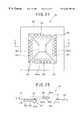
- FIG. 1is a diagrammatic view showing a resin-sealed semiconductor device according to an embodiment of the invention.
- FIG. 2is a perspective view of an inner constitution of the resin-sealed semiconductor device shown in FIG. 1 .
- FIGS. 3 to 8are diagrammatic views showing other embodiments of the resin-sealed semiconductor device of the invention.
- FIG. 9is a perspective view of an inner constitution of the resin-sealed semiconductor device shown in FIG. 8 .
- FIG. 10is a diagrammatic view showing another embodiment of the resin-sealed semiconductor device of the invention.
- FIG. 11is a sectional view diagrammatically showing another embodiment of the resin-sealed semiconductor device of the invention.
- FIG. 12is a plan view showing an inner constitution of the resin-sealed semiconductor device shown in FIG. 11 .
- FIG. 13is a sectional view diagrammatically showing another embodiment of the resin-sealed semiconductor device of the invention.
- FIG. 14is a plan view showing an embodiment of a circuit member of the invention.
- FIG. 15is a vertical sectional view of the circuit member taken along line A—A in FIG. 14 .
- FIGS. 16 and 17are sectional views showing other embodiments of the circuit member of the invention.
- FIG. 18is a plan view showing another embodiment of the circuit member of the invention.
- FIG. 19is a vertical sectional view of the circuit member taken along line B—B in FIG. 18 .
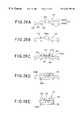
- FIGS. 20A, 20 B, 20 C, 20 D, 20 E, 21 A, 21 B, 21 C, 21 D, 21 E, 22 A, 22 B, 22 C, 22 D, 22 E, 23 A, 23 B, 23 C, 23 D, 23 Eare process diagrams showing examples of manufacturing the circuit member of the invention.
- FIG. 24is a plan view showing another embodiment of the circuit member of the invention.
- FIG. 25is a vertical sectional view of the circuit member taken along line C—C in FIG. 24 .
- FIGS. 26A, 26 B, 26 C, 26 Dis a process diagram showing an example of manufacturing the circuit member of the invention shown in FIGS. 24 and 25.
- FIGS. 27A, 27 B, 27 C, 27 D, 27 Eis a process diagram showing an example of a method of manufacturing the resin-sealed semiconductor device of the invention.
- FIGS. 28A, 28 B, 28 C, 28 D, 28 E 28is a process diagram showing another example of the method of manufacturing the resin-sealed semiconductor device according to the invention.
- FIG. 1is a diagrammatic view showing an embodiment of the resin-sealed semiconductor device according to the invention
- FIG. 2is a perspective view showing an inner constitution of the resin-sealed semiconductor device shown in FIG. 1 .
- plural terminal portions 2are arranged electrically independent of one another in two rows two-dimensionally substantially in a plane.
- a die pad 4is disposed in a substantially middle portion of the arranged terminal portions 2 .
- the die pad 4has a rectangular surface configuration.
- a face opposite to a terminal face of a semiconductor element 7is fixed and mounted via an adhesive 6 onto a surface 4 a of the die pad 4 .
- the terminal portion 2has an inner terminal 2 A on a surface and an outer terminal 2 B on a rear face with the inner and outer terminals being integrally formed.
- an exposed surface 2 a of each inner terminal 2 Ais positioned substantially on a plane.
- the exposed surface 2 ais provided with a silver plating layer 3 .
- a gold plating layer, a palladium plating layer or the likemay be formed.
- the die pad 4is thinner than the terminal portion 2 .
- a surface 4 a of the die pad 4is disposed in the same plane as a plane formed by the exposed surface 2 a of each inner terminal 2 A.
- a rear face 4 bis positioned inside an exposed surface 2 b of the outer terminal 2 B.
- terminals 7 a of the semiconductor element 7 mounted on the die pad 4are connected via wires 8 to the inner terminals 2 A (silver plating layers 3 ) of the terminal portions 2 .
- the terminal portions 2 , the die pad 4 , the semiconductor element 7 and the wires 8are sealed by a sealing member 9 in such a manner that the outer terminals 2 B are partially exposed to the outside.
- a sealing resin material for use in the resin-sealed semiconductor devicecan be used. In the embodiment shown in FIG. 1, only the exposed surfaces 2 b of the outer terminals 2 B are exposed to the outside.
- FIG. 3is a diagrammatic view showing another embodiment of the resin-sealed semiconductor device of the invention.
- a resin-sealed semiconductor device 1 ′ of the inventionis constituted by forming outer electrodes 10 of solder materials onto the exposed surfaces 2 b of the outer terminals 2 B of the aforementioned resin-sealed semiconductor device 1 .
- a BGAball grid array
- FIG. 4is a diagrammatic view showing another embodiment of the resin-sealed semiconductor device of the invention.
- a resin-sealed semiconductor device 11 of the invention shown in FIG. 4plural terminal portions 12 are arranged two-dimensionally in two rows substantially on a plane and electrically independent of one another.
- a die pad 14is disposed in a substantially middle portion of the arranged terminal portions 12 .
- the die pad 14has a rectangular surface configuration.
- a face opposite to a terminal face of a semiconductor element 17is fixed and mounted via an adhesive 16 onto a surface 14 a of the die pad 14 .
- the terminal portion 12has an inner terminal 12 A on a surface and an outer terminal 12 B on a rear face with the inner and outer terminals being integrally formed.
- an exposed surface 12 a of each inner terminal 12 Ais positioned substantially on a plane.
- the exposed surface 12 ais provided with a silver plating layer 13 .
- the die pad 14is as thick as the terminal portion 12 .
- a surface 14 a of the die pad 14is disposed in the same plane as a plane formed by the exposed surface 12 a of each inner terminal 12 A.
- a rear face 14 bis positioned in the same plane as a plane formed by an exposed surface 12 b of the outer terminal 12 B.
- terminals 17 a of the semiconductor element 17 mounted on the die pad 14are connected via wires 18 to the inner terminals 12 A (silver plating layers 13 ) of the terminal portions 12 .
- the terminal portions 12 , the die pad 14 , the semiconductor element 17 and the wires 18are sealed by a sealing member 19 in such a manner that the portions (exposed surfaces 12 b ) of the outer terminals 12 B and the rear face 14 b of the die pad 14 are exposed to the outside.
- the resin-sealed semiconductor device 11heat generated by the semiconductor element 17 is conducted to the die pad 14 which has a high thermal conductivity. Thereafter, the heat is efficiently radiated via the die pad 14 to the outside.
- the resin-sealed semiconductor device 11thus has a remarkably good radiation property.
- FIG. 5is a diagrammatic view showing another embodiment of the resin-sealed semiconductor device of the invention.
- a resin-sealed semiconductor device 21 of the invention shown in FIG. 5plural terminal portions 22 are arranged two-dimensionally in two rows substantially on a plane and electrically independent of one another.
- a die pad 24is disposed in a substantially middle portion of the arranged terminal portions 22 .
- the die pad 24has a rectangular surface configuration.
- a face opposite to a terminal face of a semiconductor element 27is fixed and mounted via an adhesive 26 onto a surface 24 a of the die pad 24 .
- the terminal portion 22has an inner terminal 22 A on a surface and an outer terminal 22 B on a rear face with the inner and outer terminals being integrally formed.
- an exposed surface 22 a of each inner terminal 22 Ais positioned substantially on a plane.
- the exposed surface 22 ais provided with a silver plating layer 23 .
- the die pad 24is thinner than the terminal portion 22 .
- a surface 24 a of the die pad 24is disposed outside a plane formed by the exposed surface 22 a of each inner terminal 22 A.
- a rear face 24 b of the die pad 24is positioned in the same plane as a plane formed by an exposed surface 22 b of the outer terminal 22 B.
- terminals 27 a of the semiconductor element 27 mounted on the die pad 24are connected via wires 28 to the inner terminals 22 A (silver plating layers 23 ) of the terminal portions 22 .
- the terminal portions 22 , the die pad 24 , the semiconductor element 27 and the wires 28are sealed by a sealing member 29 in such a manner that the portions (exposed surfaces 22 b ) of the outer terminals 22 B and the rear face 24 b of the die pad 24 are exposed to the outside.
- the resin-sealed semiconductor device 21heat generated by the semiconductor element 27 is conducted to the die pad 24 which has a high thermal conductivity. Thereafter, the heat is efficiently radiated via the die pad 24 to the outside.
- the resin-sealed semiconductor device 21thus has a remarkably good radiation property. Also, there is provided a large allowance in loop height of each wire 28 for connecting each terminal 27 a of the semiconductor element 27 and each inner terminal 22 A (silver plating layer 23 ) of the terminal portion 22 .
- FIGS. 6 and 7are diagrammatic views showing other embodiments of the resin-sealed semiconductor device of the invention.
- a resin-sealed semiconductor device 11 ′ of the invention shown in FIG. 6is constituted by forming outer electrodes 20 constituted of solder materials onto the exposed surfaces 12 b of the outer terminals 12 B of the aforementioned resin-sealed semiconductor device 11 .
- a resin-sealed semiconductor device 21 ′ of the invention shown in FIG. 7is constituted by forming outer electrodes 30 constituted of solder materials onto the exposed surfaces 22 b of the outer terminals 22 B of the aforementioned resin-sealed semiconductor device 21 .
- These resin-sealed semiconductor devices 11 ′ and 21 ′are BGA (ball grid array) semiconductor devices.
- the outer terminals 12 B or 22 Bare electrically connected to an outer circuit by melting and solidifying the outer electrodes 20 or 30 .
- FIG. 8is a diagrammatic view showing another embodiment of the resin-sealed semiconductor device of the invention
- FIG. 9is a perspective view showing an inner constitution of the resin-sealed semiconductor device shown in FIG. 8
- a resin-sealed semiconductor device 31 shown in FIGS. 8 and 9plural terminal portions 32 are arranged two-dimensionally in two rows substantially on a plane and electrically independent of one another.
- a face opposite to a terminal face of a semiconductor element 37is fixed and mounted via an insulating adhesive 36 or an insulating adhesive film 36 onto leads 35 which are integrally interconnected with the terminal portions 32 for mounting the semiconductor element thereon.
- the terminal portion 32has an inner terminal 32 A on a surface and an outer terminal 32 B on a rear face with the inner and outer terminals being integrally formed.
- an exposed surface 32 a of each inner terminal 32 Ais positioned substantially on a plane.
- the exposed surface 32 ais provided with a silver plating layer 33 .
- the lead 35is integrally interconnected with each terminal portion 32 and is thinner than the terminal portion 32 .
- a surface 35 a of the lead 35forms the same plane as a plane which is formed by the exposed surface 32 a of each inner terminal 32 A.
- terminals 37 a of the semiconductor element 37 mounted on the surfaces 35 a of the leads 35are connected via wires 38 to the inner terminals 32 A (silver plating layers 33 ) of the terminal portions 32 .
- terminal portions 32 , the leads 35 , the semiconductor element 37 and the wires 38are sealed by a sealing member 39 in such a manner that the portions (exposed surfaces 32 b ) of the outer terminals 32 B are exposed to the outside.
- FIG. 10is a diagrammatic view showing another embodiment of the resin-sealed semiconductor device of the invention.
- a resin-sealed semiconductor device 31 ′ of the invention shown in FIG. 10is constituted by forming outer electrodes 40 constituted of solder materials onto the exposed surfaces 32 b of the outer terminals 32 B of the aforementioned resin-sealed semiconductor device 31 . Thereby, a BGA (ball grid array) semiconductor device is formed.
- the outer terminals 32 Bare electrically connected to an outer circuit by melting and solidifying the outer electrodes 40 .
- Each of the resin-sealed semiconductor devices of the invention shown in FIGS. 1 to 10has a small difference between its entire size and an area of the semiconductor element.
- the miniaturized semiconductor deviceis realized.
- the thickness of the semiconductor deviceis reduced to about 1 mm or less. The reduction in thickness can be simultaneously achieved.
- the terminal portionsare arranged along a pair of sides of the semiconductor element, to which the arrangement is not limited.
- the terminals of the semiconductor elementare arranged along four sides of the semiconductor element.
- the terminal portionsare arranged two-dimensionally along the periphery of the semiconductor element.
- a nickel plating layer and a palladium plating layermay be sequentially laminated at least on the resin sealed region.
- the nickel plating layer and the palladium plating layerare formed in order on the roughed surface.
- adhesionis enhanced as compared with the case where the sealing resin material directly plats on the copper or copper-base alloy material.
- the nickel plating layerprevents copper from being dispersed on the bonded face.
- the nickel plating layerserves as a base layer when the palladium layer is laminated on the copper or copper-base alloy material.
- a chemical polishing processis available in which by etching the surface with an organic acid liquid or another etching liquid, fine irregularities are formed on the surface. This process is not restrictive.
- the surface of the copper or copper-base alloy materialhas a center line average roughness Ra of 1.0 ⁇ m or more according to JIS B0601. Especially the adhesion of the copper or copper-base alloy material to the nickel plating layer is improved. Also, when the center line average roughness Ra according to JIS B0601 on the surface of the nickel plating layer is set to 0.045 ⁇ m or more, especially the adhesion of the nickel plating layer to the palladium plating layer is improved.
- a silver or another noble metal plating layermay be formed on the palladium plating layer in the wire bonded region and the die bonded region.
- the palladium plating layermay be formed directly on the iron-base alloy material.
- the adhesion between the iron-base alloy material and the palladium plating layeris preferably raised.
- FIG. 11is a sectional view diagrammatically showing another embodiment of the resin-sealed semiconductor device of the invention
- FIG. 12is a plan view showing an inner constitution of the resin-sealed semiconductor device shown in FIG. 11 .
- a sealing member 49is shown by an imaginary line (two-dot chain line) in FIG. 11 .
- plural terminal portions 42are arranged electrically independent of one another two-dimensionally substantially in a plane.
- a die pad 44is disposed in a substantially middle portion of the arranged terminal portions 42 .
- the die pad 44has a rectangular surface configuration.
- a face opposite to a terminal face of a semiconductor element 47is fixed and mounted via an adhesive 46 onto a rear face 44 b of the die pad 44 .
- the terminal portion 42has an inner terminal 42 A on a surface and an outer terminal 42 B on a rear face with the inner and outer terminals being integrally formed.
- an exposed surface 42 a of each inner terminal 42 Ais positioned substantially on a plane.
- the exposed surface 42 ais provided with a silver plating layer 43 .
- the die pad 44is thinner than the terminal portion 42 .
- each terminal 47 a of the semiconductor element 47 fixed on the rear face 44 b of the die pad 44is disposed on the substantially same plane as a plane formed by the inner terminal 42 A of the terminal portion 42 (plane formed by the silver plating layer 43 ). Therefore, there is provided a large allowance in loop height of each wire 48 for connecting each terminal 47 a of the semiconductor element 47 and each inner terminal 42 A (silver plating layer 43 ) of the terminal portion 42 .
- the terminal portions 42 , the die pad 44 , the semiconductor element 47 and the wires 48are sealed by the sealing member 49 in such a manner that the outer terminals 42 B are partially exposed to the outside.
- a known sealing resin material for use in the resin-sealed semiconductor devicecan be used for the sealing member 49 .
- only the exposed outer terminals 42 Bare provided with outer electrodes 50 constituted of solder materials. In this manner, a BGA (ball grid array) semiconductor device is formed.
- the die pad 44serves as a radiating plate of the semiconductor element 47 .
- the semiconductor device 41when the semiconductor device 41 is mounted on the circuit substrate with the outer electrodes 50 , heat generated in the semiconductor element 47 is conducted to the die pad 44 which has a high thermal conductivity. The heat is efficiently removed by a cooling air current which flows in an upper portion of the resin-sealed semiconductor device 41 . Therefore, the resin-sealed semiconductor device 41 has a remarkably good radiation property.
- the sealing member 49may be provided in such a manner that the surface 44 a of the die pad 44 is exposed to the outside.
- the terminal portions 42 and the die pad 44are formed of a copper or a copper-base alloy, a nickel plating layer and a palladium plating layer may be laminated at least on the resin sealed region. Also, when the terminal portions 42 and the die pad 44 are formed not of the copper or copper-base alloy material but of Alloy 42 (41% Ni-iron) or another iron-base alloy material, the palladium plating layer may be formed directly on the iron-base alloy material.
- a circuit member of the inventionwill be described.
- FIG. 14is a plan view showing an embodiment of the circuit member of the invention
- FIG. 15is a vertical sectional view of the circuit member taken along line A—A in FIG. 14
- a region surrounded by a chain line in FIG. 14is a region of the circuit member for use in the manufacture of the semiconductor device.
- a circuit member 51 of the inventionis provided with an outer frame member 52 , plural terminal portions 54 independently connected via connection leads 53 from the outer frame member 52 and a die pad 55 connected via connecting leads 53 ′ to the outer frame member 52 .
- the outer frame member 52has rectangular contour and inner opening configurations.
- the connecting leads 53are extended from a pair of opposite sides of the inner opening of the outer frame member 52 in the same plane. Also, the connecting leads 53 ′ are extended from the other pair of opposite sides of the inner opening of the outer frame member 52 in the same plane.
- the terminal portion 54is connected to a tip end of the connecting lead 53 , and has an inner terminal 54 A on a surface and an outer terminal 54 B on a rear face with the inner and outer terminals being integrally formed.
- the die pad 55is supported by the two connecting leads 53 ′ which are extended from the pair of opposite sides of the inner opening of the outer frame member 52 in the same plane.
- the die pad 55is thinner than the terminal portion 54 .
- a surface 55 a of the die pad 55is in the same plane as a plane formed by each inner terminal 54 A, and a rear face 55 b thereof is positioned inside a plane formed by the outer terminal 54 B.
- the die pad 55is as thick as the terminal portion 54 .
- the surface 55 a of the die pad 55is in the same plane as a plane formed by each inner terminal 54 A, while the rear face 55 b thereof may be in the same plane as the plane formed by the outer terminal 54 B.
- the die pad 55is thinner than the terminal portion 54 .
- the surface 55 a of the die pad 55is positioned inside the plane formed by the inner terminal 54 A, while the rear face 55 b thereof is in the same plane as the plane formed by the outer terminal 54 B.
- the circuit member 51 , 51 ′ or 51 ′′may be formed of Alloy 42 (41% Ni—Fe), a copper, a copper-base alloy or the like.
- circuit member 51 , 51 ′ or 51 ′′ of the inventionis formed of a copper or a copper-base alloy
- a nickel plating layer and a palladium plating layermay be laminated at least on the resin sealed region during the manufacture of the semiconductor device, as described above in the resin-sealed semiconductor device of the invention shown in FIGS. 1 to 10 .
- the circuit member 51 , 51 ′ or 51 ′′is formed not of the copper or copper-base alloy material but of Alloy 42 (41% Ni—Fe) or another iron-base alloy material
- the palladium plating layermay be formed directly on the iron-base alloy material.
- an insulating adhesive double-coated tapemay be provided on the surface 55 a of the die pad 55 .
- the adhesive double-coated tape availableis an adhesive double-coated tape of an insulating base film having adhesive layers formed on both faces thereof, for example, an adhesive double-coated tape UX1W (manufactured by Kabushiki Kaisha Tomoegawa Seishisho) of UPLEX (insulating base film manufactured by Ube Kosan Kabushiki Kaisha) having RXF (adhesive manufactured by Kabushiki Kaisha Tomoegawa Seisho) layers on both faces thereof.
- the resin-sealed semiconductor device 1 or 1 ′can be manufactured.
- the resin-sealed semiconductor device 11 or 11 ′can be manufactured.
- the resin-sealed semiconductor device 21 or 21 ′can be manufactured.
- FIG. 18is a plan view showing another embodiment of the circuit member of the invention, while FIG. 19 is a vertical sectional view of the circuit member taken along line B—B in FIG. 18 . Additionally, a region surrounded by a chain line in FIG. 18 is a region of the circuit member for use in the manufacture of the semiconductor device.
- a circuit member 61 of the inventionis provided with an outer frame member 62 , plural terminal portions 64 independently connected via connection leads 63 from the outer frame member 62 and leads 66 integrally interconnected with the terminal portions 64 for mounting a semiconductor element thereon.
- the outer frame member 62has rectangular contour and inner opening configurations.
- the connecting leads 63are extended from a pair of opposite sides of the inner opening of the outer frame member 62 into the same plane.
- the terminal portion 64has an inner terminal 64 A on a surface and an outer terminal 64 B on a rear face with the inner and outer terminals being integrally formed.
- the leads 66are integrally interconnected with tip ends of the terminal portions 64 , and positioned in the same plane as a plane formed by the terminal portions 64 .
- the circuit member 61may be formed of Alloy 42 (41% Ni—Fe), a copper, a copper-base alloy or the like. Also, in the same manner as the circuit member 51 , 51 ′ or 51 ′′, when the circuit member 61 is formed of a copper or a copper-base alloy, a nickel plating layer and a palladium plating layer may be laminated at least on the resin sealed region during the manufacture of the semiconductor device. Also, when the circuit member 61 is formed not of the copper or copper-base alloy material but of Alloy 42 (41% Ni—Fe) or another iron-base alloy material, the palladium plating layer may be formed directly on the iron-base alloy material.
- an insulating adhesive double-coated tapemay be provided on a surface 66 a of the lead 66 .
- the resin-sealed semiconductor device 31 or 31 ′can be manufactured.
- FIGS. 20 to 22are process diagrams showing an example of manufacturing the circuit member 51 , 51 ′ or 51 ′′.
- a photosensitive resistis applied onto a surface and a rear face of a substrate 71 and dried to form photosensitive resist layers 72 (FIGS. 20A, 21 A, 22 A). After the photosensitive resist layers 72 are exposed via desired photo masks, images are developed to form resist patterns 72 A and 72 B (FIGS. 20B, 21 B, 22 B).
- the substrate 71As aforementioned, Alloy 42 (41% Ni—Fe), copper, copper-base alloy or another metal substrate with a thickness of 100 to 250 ⁇ m can be used.
- the substrate 71 with both faces degreased or cleaned beforehandis preferably used.
- a palladium plating layer or a combination of a nickel plating layer and a palladium plating layermay be laminated on the substrate.
- a conventional known resistcan be used such as a casein resist using a photosensitive material of potassium dichromate, a negative liquefied resist (PMER-N) manufactured by Tokyo Ouka Kogyo Kabushiki Kaisha and the like.
- the substrate 71is etched with an etching liquid.
- the etchingproceeds as shown in FIGS. 20C, 21 C or 22 C, and completes as shown in FIGS. 20D, 21 D or 22 D.
- etching liquidan aqueous ferric chloride solution is usually used.
- the etching liquidis applied to both faces of the substrate 71 through spray etching. By adjusting an etched quantity in the etching process, a thickness of a small thickness portion 73 can be adjusted.
- the resist patterns 72 A and 72 Bare peeled and removed to obtain the circuit member 51 , 51 ′ or 51 ′′ of the invention (FIGS. 20E, 21 E, 22 E).
- FIG. 23is a process diagram showing an example of manufacturing the circuit member 61 .
- a photosensitive resistis applied onto a surface and a rear face of a substrate 81 and dried to form photosensitive resist layers 82 (FIG. 23 A).
- photosensitive resist layers 82are exposed via desired photo masks, images are developed to form resist patterns 82 A and 82 B (FIG. 23 B).
- the substrate 81the same as the substrate 71 can be used.
- the substrate 81is etched with an etching liquid.
- the etchingproceeds as shown in FIG. 23C, and completes as shown in FIG. 23 D.
- As the etching liquidan aqueous ferric chloride solution is usually used.
- the etching liquidis applied to both faces of the substrate 81 through spray etching. By adjusting an etched quantity in the etching process, a thickness of a small thickness portion 83 can be adjusted.
- the resist patterns 82 A and 82 Bare peeled and removed to obtain the circuit member 61 of the invention (FIG. 23 E).
- FIG. 24is a plan view showing another embodiment of the circuit member of the invention
- FIG. 25is a vertical sectional view of the circuit member taken along line C—C in FIG. 24
- a circuit member 91 of the inventionis provided with an outer frame member 92 , plural terminal portions 94 independently connected via connection leads 93 from the outer frame member 92 and a die pad 95 connected via connection leads 93 ′ from the outer frame member 92 .
- the outer frame member 92has rectangular contour and inner opening configurations.
- the connecting leads 93are extended from sides of the inner opening of the outer frame member 92 in the same plane.
- the terminal portion 94is provided on a tip end of the connection lead 93 , and has an inner terminal 94 A on a surface and an outer terminal 94 B on a rear face with the inner and outer terminals being integrally formed. As shown in FIG. 25, the inner terminal 94 A is provided with a silver plating layer 97 . The silver plating layer 97 on the inner terminal 94 A is positioned on the same plane (plane shown by a dashed line P 2 in FIG. 25 ).
- the die pad 95is supported by the four connecting leads 93 ′ which are extended from corners of the inner opening of the outer frame member 92 . Then, the die pad 95 is protruded above the inner terminal 94 A (upward in FIG. 25 ).
- a gap Gis formed between a plane formed by a surface 95 a (shown by a dashed line PI in FIG. 25) of the die pad 95 and the silver plating layer 97 on each inner terminal 94 A.
- a size of the gap Gcan be set, for example, in a range of about 100 to 500 ⁇ m.
- the circuit member 91may be formed of Alloy 42 (41% Ni—Fe), a copper, a copper-base alloy or the like. Also, when the circuit member 91 of the invention is formed of a copper or a copper-base alloy, a nickel plating layer and a palladium plating layer may be laminated at least on the resin sealed region during the manufacture of the semiconductor device in the same manner as in the resin-sealed semiconductor devices of the invention shown in FIGS. 1 to 10 . When the circuit member 91 of the invention is formed not of the copper or copper-base alloy material but of Alloy 42 (41% Ni—Fe) or another iron-base alloy material, the palladium plating layer may be formed directly on the iron-base alloy material.
- an insulating adhesive double-coated tapemay be provided on a rear face 95 b of the die pad 95 .
- FIG. 26is a process diagram showing an example of manufacturing the circuit member 91 of the invention shown in FIGS. 24 and 25. Each process is shown in a vertical sectional view of the circuit member corresponding to FIG. 25 .
- a photosensitive resistis applied onto a surface and a rear face of a substrate 101 and dried. After exposure is performed via desired photo masks, images are developed to form resist patterns 102 A and 102 B (FIG. 26 A).
- the substrate 101the same as the substrate 71 can be used.
- the photosensitive resista conventional known resist can be used.
- the substrate 101is etched with an etching liquid (FIG. 26 B).
- an aqueous ferric chloride solutionis usually used as the etching liquid.
- the etching liquidis applied to both faces of the substrate 101 through spray etching.
- the resist patterns 102 A and 102 Bare peeled and removed to obtain a circuit member pattern in which the terminal portions 94 and the die pad 95 are integrally interconnected via connection leads 3 and 3 ′ (not shown) to the outer frame member 92 (FIG. 26C) .
- the inner terminal 94 A and the surface 95 a of the die pad 95are positioned in the same plane.
- the die pad 95is protruded from the inner terminal 94 A by using a predetermined metal mold. A gap is formed between the surface 95 a of the die pad 95 and the surface of the inner terminal 94 A (FIG. 26 D). Consequently, the circuit member 91 of the invention can be obtained.
- FIG. 27is a process diagram showing an embodiment of the manufacture method of the resin-sealed semiconductor device according to the invention. Each process is shown in a constitutional diagram of the resin-sealed semiconductor device corresponding to FIG. 1 .
- the circuit member 51 shown in FIGS. 14 and 15is prepared (FIG. 27 A). Subsequently, after cleaning the circuit member 51 , the silver plating layer 3 is formed on the surface of the inner terminal 54 A (FIG. 27 B). Additionally, instead of the silver plating layer 3 , a gold plating layer, a palladium plating layer or the like may be formed.
- the face opposite to the terminal face of the semiconductor element 7is fixed via the insulating adhesive material 6 onto the surface 55 a of the die pad 55 .
- the semiconductor element 7is thus mounted.
- the terminals 7 a of the mounted semiconductor element 7are electrically connected via the wires 8 to the silver plating layers 3 on the inner terminals 54 A of the terminal portions 54 in the circuit member 51 (FIG. 27 C).
- the terminal portions 54 , the die pad 55 , the semiconductor element 7 and the wires 8are sealed in the sealing member 9 in such a manner that the portions ( 54 b ) of the outer terminals 54 B are exposed to the outside (FIG. 27 D).
- the outer electrodes of solder materialsare formed on the exposed outer terminals 54 b. Then, the resin-sealed semiconductor device 1 ′ of the invention shown in FIG. 3 can be obtained.
- the outer electrodes of solder materialscan be formed by applying a solder paste through screen printing, reflowing or the like. Only a quantity of solder necessary for connecting the circuit substrate and the resin-sealed semiconductor device may be obtained.
- FIG. 28is a process diagram showing another embodiment of the manufacture method of the resin-sealed semiconductor device according to the invention. Each process is shown in a constitutional diagram of the resin-sealed semiconductor device corresponding to FIG. 8 .
- the circuit member 61 shown in FIGS. 18 and 19is prepared (FIG. 28 A). Subsequently, after cleaning the circuit member 61 , the silver plating layer 33 is formed on the surface of the inner terminal 64 A (FIG. 28 B). Additionally, instead of the silver plating layer 33 , a gold plating layer, a palladium plating layer or the like may be formed.
- the face opposite to the terminal face of the semiconductor element 37is fixed via the insulating adhesive material 36 onto the surfaces 66 a of the leads 66 .
- the semiconductor element 37is thus mounted.
- the terminals 37 a of the mounted semiconductor element 37are electrically connected via the wires 38 to the silver plating layers 33 on the inner terminals 64 A of the terminal portions 64 in the circuit member 61 (FIG. 28 C).
- terminal portions 64 , the leads 66 , the semiconductor element 37 and the wires 38are sealed in the sealing member 39 in such a manner that the portions ( 64 b ) of the outer terminals 64 B are exposed to the outside (FIG. 28 D).
- the outer electrodes of solder materialsare formed on the exposed outer terminals 64 b. Then, the resin-sealed semiconductor device 31 ′ of the invention shown in FIG. 10 can be obtained.
- the outer electrodes of solder materialscan be formed by applying a solder paste through screen printing, reflowing or the like. Only a quantity of solder necessary for connecting the circuit substrate and the resin-sealed semiconductor device may be used.
- circuit member 51 shown in FIG. 14 and 15 and the circuit member 61 shown in FIGS. 18 and 19are used. Needless to say, in the method of manufacturing the resin-sealed semiconductor device according to the invention, any circuit member of the invention can be used.
- a circuit member of the inventionwas prepared in the etching method shown in FIG. 20 .
- an ultraviolet hardening resistPMER-N manufactured by Tokyo Ouka Kogyo Kabushiki Kaisha
- resist layers on the surface and the rear face of the substratewere exposed via predetermined photo masks to develop images and form resist patterns.
- both the faces of the substratewere spray-etched by using an aqueous ferric chloride solution.
- the resist patternswere peeled and removed by using an organic alkaline solution.
- a terminal portion of the circuit memberwas 0.2 mm thick, while a connection lead portion was 0.05 mm thick.
- a silver plating layerwas formed on an inner terminal face of the prepared circuit member.
- an insulating adhesive double-coated tapeUH1W manufactured by Tomoegawa Seishisho Kabushiki Kaisha
- UH1Wmanufactured by Tomoegawa Seishisho Kabushiki Kaisha
- a face opposite to a terminal face of a semiconductor elementwas pressed onto the adhesive double-coated tape, heated (140° C.) and fixed thereto.
- the semiconductor elementwas thus mounted.
- the silver plating layers on the inner terminals of the circuit memberwere connected via gold wires to terminals of the mounted semiconductor element.
- the terminal portions, the die pad, the semiconductor element and the gold wireswere sealed in a resin material (MP-7400 manufactured by Nitto Denko Iabushiki Kaisha) in such a manner that outer terminals were partially exposed to the outside.
- MP-7400manufactured by Nitto Denko Iabushiki Kaisha
- a resin-sealed semiconductor device prepared in this mannerhad no problem about its quality.
- a resin-sealed semiconductor devicewas prepared in the same manner as the first example except in that instead of the Alloy 42 (41% Ni—Fe), a copper plate (EFTEC64T-1 ⁇ 2H manufactured by Furukawa Denki Kogyo Kabushiki Kaisha) was used.
- the resin-sealed semiconductor device prepared in this mannerhad no problem about its quality.
- a circuit member of the inventionwas prepared in the etching method shown in FIG. 23 .
- an ultraviolet hardening resistPMER-N manufactured by Tokyo Ouka Kogyo Kabushiki Kaisha
- resist layers on the surface and the rear face of the substratewere exposed via predetermined photo masks to develop images and form resist patterns.
- both the faces of the substratewere spray-etched by using an aqueous ferric chloride solution.
- the resist patternswere peeled and removed by using an organic alkaline solution.
- a terminal portion of the circuit memberwas 0.2 mm thick, while a connection lead portion or a lead was 0.05 mm thick.
- a silver plating layerwas formed on an inner terminal face of the prepared circuit member.
- an insulating adhesive double-coated tapeUH1W manufactured by Tomoegawa Seishisho Kabushiki Kaisha
- UH1Wmanufactured by Tomoegawa Seishisho Kabushiki Kaisha
- a face opposite to a terminal face of a semiconductor elementwas pressed onto the adhesive double-coated tape, heated (140° C.) and fixed thereto.
- the semiconductor elementwas thus mounted.
- the silver plating layers on the inner terminals of the circuit memberwere connected via gold wires to terminals of the mounted semiconductor element.
- the terminal portions, the leads, the semiconductor element and the gold wireswere sealed in a resin material (MP-7400 manufactured by Nitto Denko Kabushiki Kaisha) in such a manner that outer terminals were partially exposed to the outside.
- a resin-sealed semiconductor device prepared in this mannerhad no problem about its quality.
- a circuit memberwas prepared in the same manner as the first example except in that instead of the Alloy 42 (41% Ni—Fe), a copper plate (EFTEC64T-1 ⁇ 2H manufactured by Furukawa Denki Kogyo Kabushiki Kaisha) was used. A terminal portion was 0.2 mm thick, and a connection lead portion was 0.1 mm thick.
- the circuit memberwas subjected to a surface roughing process.
- a micro-etching process liquid (CZ8100) manufactured by MEC Kabushiki Kaishathe circuit member was subjected to a surface roughing process.
- the entire surface of the circuit memberhad a center line average roughness Ra of 0.2 ⁇ m according to JIS B0601.
- a nickel plating layer(1 ⁇ m thick) was formed on the circuit member.
- the center line average roughness Ra of JIS B0601 of the nickel plating layerwas 0.050 ⁇ m.
- the resin-sealed semiconductor device prepared in this mannerhad no problem about its quality.
- a circuit member of the inventionwas prepared in the etching method shown in FIG. 26 .
- an ultraviolet hardening resistPMER-N manufactured by Tokyo Ouka Kogyo Kabushiki Kaisha
- resist layers on the surface and the rear facewere exposed via predetermined photo masks to develop images and form resist patterns.
- both the faces of the copper platewere spray-etched by using an aqueous ferric chloride solution. After cleaning, the resist patterns were peeled and removed by using an organic alkaline solution.
- a silver plating layer(about 5 ⁇ m thick) was formed on an inner terminal face
- a die padwas protruded from the inner terminal face by using a predetermined metallic mold. Thereby, a gap of about 250 ⁇ m was formed between the surface of the die pad and the silver plating layer on the inner terminal.
- an insulating adhesive double-coated tape(UH1W manufactured by Tomoegawa Seishisho Kabushiki Kaisha) was placed on a rear face of the die pad to obtain the circuit member.
- a terminal face of a semiconductor element(about 0.25 mm thick) was pressed onto the adhesive double-coated tape on the rear face of the die pad of the circuit member, heated (140° C.) and fixed thereto.
- the semiconductor elementwas thus mounted.
- the silver plating layers on the inner terminals of the circuit memberwere connected via gold wires to terminals of the mounted semiconductor element.
- the terminal portions, the die pad, the semiconductor element and the gold wireswere sealed in a resin material (MP-7400 manufactured by Nitto Denko Kabushiki Kaisha) in such a manner that outer terminals were partially exposed to the outside.
- the number of the outer terminals in a semiconductor device prepared in this mannerwas 80 pins.
- a contour dimensionwas 10 mm sides.
- the semiconductor devicewas compact-sized. Additionally, a thickness was 0.8 mm. The semiconductor device was also very thin.
Landscapes
- Engineering & Computer Science (AREA)
- Physics & Mathematics (AREA)
- Condensed Matter Physics & Semiconductors (AREA)
- General Physics & Mathematics (AREA)
- Computer Hardware Design (AREA)
- Microelectronics & Electronic Packaging (AREA)
- Power Engineering (AREA)
- Manufacturing & Machinery (AREA)
- Geometry (AREA)
- Lead Frames For Integrated Circuits (AREA)
Abstract
Description
Claims (62)
Applications Claiming Priority (8)
| Application Number | Priority Date | Filing Date | Title |
|---|---|---|---|
| JP9-097885 | 1997-04-02 | ||
| JP9788597 | 1997-04-02 | ||
| JP9201001AJPH10335566A (en) | 1997-04-02 | 1997-07-11 | Resin-sealed semiconductor device, circuit member used therefor, and method of manufacturing resin-sealed semiconductor device |
| JP9-201001 | 1997-07-11 | ||
| JP20552097AJPH1140720A (en) | 1997-07-16 | 1997-07-16 | Circuit member and resin-sealed semiconductor device using the circuit member |
| JP9-205520 | 1997-07-16 | ||
| JP9-287993 | 1997-10-03 | ||
| JP28799397AJP3699573B2 (en) | 1997-10-03 | 1997-10-03 | Semiconductor device, circuit member used therefor, and manufacturing method thereof |
Publications (1)
| Publication Number | Publication Date |
|---|---|
| US6201292B1true US6201292B1 (en) | 2001-03-13 |
Family
ID=27468582
Family Applications (1)
| Application Number | Title | Priority Date | Filing Date |
|---|---|---|---|
| US09/052,984Expired - LifetimeUS6201292B1 (en) | 1997-04-02 | 1998-04-01 | Resin-sealed semiconductor device, circuit member used therefor |
Country Status (2)
| Country | Link |
|---|---|
| US (1) | US6201292B1 (en) |
| KR (1) | KR100297464B1 (en) |
Cited By (161)
| Publication number | Priority date | Publication date | Assignee | Title |
|---|---|---|---|---|
| US6304384B1 (en)* | 1998-10-23 | 2001-10-16 | Seiko Epson Corporation | Optical substrate, a manufacturing method therefor, and a display device using the same |
| US6342730B1 (en)* | 2000-01-28 | 2002-01-29 | Advanced Semiconductor Engineering, Inc. | Low-pin-count chip package and manufacturing method thereof |
| US6380062B1 (en)* | 2001-03-09 | 2002-04-30 | Walsin Advanced Electronics Ltd. | Method of fabricating semiconductor package having metal peg leads and connected by trace lines |
| US20020050397A1 (en)* | 2000-10-26 | 2002-05-02 | Noriaki Sakamoto | Semiconductor module and method of manufacturing the same |
| US20020076852A1 (en)* | 2000-09-22 | 2002-06-20 | Stefan Paulus | Method for manufacturing a component which is encapsulated in plastic, and a component which is encapsulated in plastic |
| US6424024B1 (en)* | 2001-01-23 | 2002-07-23 | Siliconware Precision Industries Co., Ltd. | Leadframe of quad flat non-leaded package |
| US6452255B1 (en)* | 2000-03-20 | 2002-09-17 | National Semiconductor, Corp. | Low inductance leadless package |
| US6462418B2 (en)* | 2000-09-06 | 2002-10-08 | Sanyo Electric Co., Ltd. | Semiconductor device having improved heat radiation |
| US20020149090A1 (en)* | 2001-03-30 | 2002-10-17 | Chikao Ikenaga | Lead frame and semiconductor package |
| US6483180B1 (en) | 1999-12-23 | 2002-11-19 | National Semiconductor Corporation | Lead frame design for burr-free singulation of molded array packages |
| US6495909B2 (en)* | 2000-01-05 | 2002-12-17 | Advanced Semiconductor Engineering, Inc. | Low-pin-count chip package and manufacturing method thereof |
| US20030001249A1 (en)* | 1999-06-30 | 2003-01-02 | Yoshihiko Shimanuki | Semiconductor device and a method of manufacturing the same and a mounting structure of a semiconductor device |
| US20030006492A1 (en)* | 2001-07-09 | 2003-01-09 | Kazuto Ogasawara | Semiconductor device and method of manufacturing the same |
| WO2002037563A3 (en)* | 2000-10-31 | 2003-04-17 | Motorola Inc | A leadframe and semiconductor package |
| US6589814B1 (en) | 1998-04-02 | 2003-07-08 | National Semiconductor Corporation | Lead frame chip scale package |
| US6608366B1 (en)* | 2002-04-15 | 2003-08-19 | Harry J. Fogelson | Lead frame with plated end leads |
| US6630729B2 (en)* | 2000-09-04 | 2003-10-07 | Siliconware Precision Industries Co., Ltd. | Low-profile semiconductor package with strengthening structure |
| US20030197290A1 (en)* | 1999-12-16 | 2003-10-23 | Crowley Sean Timothy | Stackable semiconductor package and method for manufacturing same |
| US6658734B2 (en)* | 1997-08-04 | 2003-12-09 | Dai Nippon Insatsu Kabushiki Kaisha | Method of manufacturing a circuit member for a resin-sealed semiconductor device |
| US20030234454A1 (en)* | 2002-06-24 | 2003-12-25 | Serafin Pedron | Integrated circuit package and method of manufacturing the integrated circuit package |
| US6677667B1 (en)* | 2000-11-28 | 2004-01-13 | National Semiconductor Corporation | Leadless leadframe package design that provides a greater structural integrity |
| US6696747B1 (en)* | 1999-10-15 | 2004-02-24 | Amkor Technology, Inc. | Semiconductor package having reduced thickness |
| US20040065905A1 (en)* | 2001-03-27 | 2004-04-08 | Jong Sik Paek | Semiconductor package and method for manufacturing the same |
| US20040097016A1 (en)* | 1998-11-20 | 2004-05-20 | Yee Jae Hak | Semiconductor package and method of making leadframe having lead locks to secure leads to encapsulant |
| US6750545B1 (en) | 2003-02-28 | 2004-06-15 | Amkor Technology, Inc. | Semiconductor package capable of die stacking |
| US20040155363A1 (en)* | 2001-12-05 | 2004-08-12 | Matsushita Electric Industrial Co., Ltd. | Resin-encapsulated semiconductor device and method for manufacturing the same |
| US6777789B1 (en) | 2001-03-20 | 2004-08-17 | Amkor Technology, Inc. | Mounting for a package containing a chip |
| US6790710B2 (en) | 2002-01-31 | 2004-09-14 | Asat Limited | Method of manufacturing an integrated circuit package |
| WO2003105223A3 (en)* | 2002-06-06 | 2004-09-16 | Philips Intellectual Property | Quad flat non-leaded package comprising a semiconductor device |
| US6794740B1 (en) | 2003-03-13 | 2004-09-21 | Amkor Technology, Inc. | Leadframe package for semiconductor devices |
| US6798047B1 (en) | 2002-12-26 | 2004-09-28 | Amkor Technology, Inc. | Pre-molded leadframe |
| US20040207054A1 (en)* | 2003-04-21 | 2004-10-21 | Motorola, Inc. | Semiconductor component for electrical coupling to a substrate, and method of manufacturing same |
| US6815806B1 (en)* | 2003-07-17 | 2004-11-09 | International Business Machines Corp. | Asymmetric partially-etched leads for finer pitch semiconductor chip package |
| US6873041B1 (en) | 2001-11-07 | 2005-03-29 | Amkor Technology, Inc. | Power semiconductor package with strap |
| US6873032B1 (en) | 2001-04-04 | 2005-03-29 | Amkor Technology, Inc. | Thermally enhanced chip scale lead on chip semiconductor package and method of making same |
| US6876068B1 (en) | 2002-09-09 | 2005-04-05 | Amkor Technology, Inc | Semiconductor package with increased number of input and output pins |
| US20050073057A1 (en)* | 2001-12-14 | 2005-04-07 | Stmicroelectronics S.R.I. | Semiconductor electronic device and method of manufacturing thereof |
| US6879034B1 (en) | 2003-05-01 | 2005-04-12 | Amkor Technology, Inc. | Semiconductor package including low temperature co-fired ceramic substrate |
| US20050093117A1 (en)* | 2003-04-11 | 2005-05-05 | Dai Nippon Printing Co., Ltd. | Plastic package and method of fabricating the same |
| US6893900B1 (en) | 1998-06-24 | 2005-05-17 | Amkor Technology, Inc. | Method of making an integrated circuit package |
| US6897550B1 (en) | 2003-06-11 | 2005-05-24 | Amkor Technology, Inc. | Fully-molded leadframe stand-off feature |
| US6919620B1 (en) | 2002-09-17 | 2005-07-19 | Amkor Technology, Inc. | Compact flash memory card with clamshell leadframe |
| US20050156292A1 (en)* | 2001-01-15 | 2005-07-21 | Paek Jong S. | Reduced size semiconductor package with stacked dies |
| US6921967B2 (en) | 2003-09-24 | 2005-07-26 | Amkor Technology, Inc. | Reinforced die pad support structure |
| US6933174B1 (en) | 2000-11-28 | 2005-08-23 | National Semiconductor Corporation | Leadless leadframe package design that provides a greater structural integrity |
| US6953988B2 (en) | 2000-03-25 | 2005-10-11 | Amkor Technology, Inc. | Semiconductor package |
| US6965159B1 (en) | 2001-09-19 | 2005-11-15 | Amkor Technology, Inc. | Reinforced lead-frame assembly for interconnecting circuits within a circuit module |
| US6965157B1 (en) | 1999-11-09 | 2005-11-15 | Amkor Technology, Inc. | Semiconductor package with exposed die pad and body-locking leadframe |
| US6967401B2 (en)* | 2000-10-05 | 2005-11-22 | Sanyo Electric Co., Ltd. | Semiconductor device, semiconductor module and hard disk |
| US6967395B1 (en) | 2001-03-20 | 2005-11-22 | Amkor Technology, Inc. | Mounting for a package containing a chip |
| US7001799B1 (en) | 2003-03-13 | 2006-02-21 | Amkor Technology, Inc. | Method of making a leadframe for semiconductor devices |
| US7005326B1 (en)* | 1998-06-24 | 2006-02-28 | Amkor Technology, Inc. | Method of making an integrated circuit package |
| US7008825B1 (en) | 2003-05-27 | 2006-03-07 | Amkor Technology, Inc. | Leadframe strip having enhanced testability |
| US7009283B1 (en)* | 1999-04-14 | 2006-03-07 | Amkor Technology, Inc. | Nonexposed heat sink for semiconductor package |
| US7030474B1 (en) | 1998-06-24 | 2006-04-18 | Amkor Technology, Inc. | Plastic integrated circuit package and method and leadframe for making the package |
| US7045883B1 (en) | 2001-04-04 | 2006-05-16 | Amkor Technology, Inc. | Thermally enhanced chip scale lead on chip semiconductor package and method of making same |
| US7045882B2 (en) | 2000-12-29 | 2006-05-16 | Amkor Technology, Inc. | Semiconductor package including flip chip |
| US7057268B1 (en) | 2004-01-27 | 2006-06-06 | Amkor Technology, Inc. | Cavity case with clip/plug for use on multi-media card |
| US7064009B1 (en) | 2001-04-04 | 2006-06-20 | Amkor Technology, Inc. | Thermally enhanced chip scale lead on chip semiconductor package and method of making same |
| US7071541B1 (en) | 1998-06-24 | 2006-07-04 | Amkor Technology, Inc. | Plastic integrated circuit package and method and leadframe for making the package |
| US7091594B1 (en) | 2004-01-28 | 2006-08-15 | Amkor Technology, Inc. | Leadframe type semiconductor package having reduced inductance and its manufacturing method |
| US20060181861A1 (en)* | 2005-02-17 | 2006-08-17 | Walker Harold Y Jr | Etched leadframe for reducing metal gaps |
| US7095103B1 (en) | 2003-05-01 | 2006-08-22 | Amkor Technology, Inc. | Leadframe based memory card |
| US7102208B1 (en) | 1999-10-15 | 2006-09-05 | Amkor Technology, Inc. | Leadframe and semiconductor package with improved solder joint strength |
| US7112474B1 (en) | 1998-06-24 | 2006-09-26 | Amkor Technology, Inc. | Method of making an integrated circuit package |
| US7138707B1 (en) | 2003-10-21 | 2006-11-21 | Amkor Technology, Inc. | Semiconductor package including leads and conductive posts for providing increased functionality |
| US7144517B1 (en) | 2003-11-07 | 2006-12-05 | Amkor Technology, Inc. | Manufacturing method for leadframe and for semiconductor package using the leadframe |
| US7170150B2 (en) | 2001-03-27 | 2007-01-30 | Amkor Technology, Inc. | Lead frame for semiconductor package |
| US7190062B1 (en) | 2004-06-15 | 2007-03-13 | Amkor Technology, Inc. | Embedded leadframe semiconductor package |
| US7192807B1 (en) | 2002-11-08 | 2007-03-20 | Amkor Technology, Inc. | Wafer level package and fabrication method |
| US7202554B1 (en) | 2004-08-19 | 2007-04-10 | Amkor Technology, Inc. | Semiconductor package and its manufacturing method |
| US7211879B1 (en) | 2003-11-12 | 2007-05-01 | Amkor Technology, Inc. | Semiconductor package with chamfered corners and method of manufacturing the same |
| US20070105281A1 (en)* | 2003-09-01 | 2007-05-10 | Nec Electronics Corporation | Leadless type semiconductor package, and production process for manufacturing such leadless type semiconductor package |
| US7217991B1 (en) | 2004-10-22 | 2007-05-15 | Amkor Technology, Inc. | Fan-in leadframe semiconductor package |
| US20070111374A1 (en)* | 2003-08-26 | 2007-05-17 | Advanced Interconnect Technologies Limited | Reversible leadless package and methods of making and using same |
| US7245007B1 (en) | 2003-09-18 | 2007-07-17 | Amkor Technology, Inc. | Exposed lead interposer leadframe package |
| US7253503B1 (en) | 1999-11-05 | 2007-08-07 | Amkor Technology, Inc. | Integrated circuit device packages and substrates for making the packages |
| US20080001264A1 (en)* | 2006-07-03 | 2008-01-03 | Texas Instruments Incorporated | Exposed top side copper leadframe manufacturing |
| US7332375B1 (en) | 1998-06-24 | 2008-02-19 | Amkor Technology, Inc. | Method of making an integrated circuit package |
| US7361533B1 (en) | 2002-11-08 | 2008-04-22 | Amkor Technology, Inc. | Stacked embedded leadframe |
| US20080135995A1 (en)* | 2006-12-08 | 2008-06-12 | Wu Hu Li | Electronic component |
| US7419855B1 (en)* | 2004-09-14 | 2008-09-02 | National Semiconductor Corporation | Apparatus and method for miniature semiconductor packages |
| US7485952B1 (en) | 2001-09-19 | 2009-02-03 | Amkor Technology, Inc. | Drop resistant bumpers for fully molded memory cards |
| US20090039486A1 (en)* | 2005-04-26 | 2009-02-12 | Yo Shimazaki | Circuit member, manufacturing method for circuit members, semiconductor device, and surface lamination structure for circuit member |
| US7507603B1 (en) | 2005-12-02 | 2009-03-24 | Amkor Technology, Inc. | Etch singulated semiconductor package |
| US7535085B2 (en) | 1999-10-15 | 2009-05-19 | Amkor Technology, Inc. | Semiconductor package having improved adhesiveness and ground bonding |
| US20090146280A1 (en)* | 2005-11-28 | 2009-06-11 | Dai Nippon Printing Co., Ltd. | Circuit member, manufacturing method of the circuit member, and semiconductor device including the circuit member |
| US7572681B1 (en) | 2005-12-08 | 2009-08-11 | Amkor Technology, Inc. | Embedded electronic component package |
| US20090230526A1 (en)* | 2008-03-14 | 2009-09-17 | Chien-Wen Chen | Advanced quad flat no lead chip package having a protective layer to enhance surface mounting and manufacturing methods thereof |
| US7598598B1 (en) | 2003-02-05 | 2009-10-06 | Amkor Technology, Inc. | Offset etched corner leads for semiconductor package |
| US20090321958A1 (en)* | 2007-12-21 | 2009-12-31 | Junji Tanaka | Semiconductor device having a simplified stack and method for manufacturing thereof |
| US20100044843A1 (en)* | 2008-08-21 | 2010-02-25 | Advanced Semiconductor Engineering, Inc. | Advanced quad flat non-leaded package structure and manufacturing method thereof |
| US7687899B1 (en) | 2007-08-07 | 2010-03-30 | Amkor Technology, Inc. | Dual laminate package structure with embedded elements |
| US7687893B2 (en) | 2006-12-27 | 2010-03-30 | Amkor Technology, Inc. | Semiconductor package having leadframe with exposed anchor pads |
| US7723210B2 (en) | 2002-11-08 | 2010-05-25 | Amkor Technology, Inc. | Direct-write wafer level chip scale package |
| US7723852B1 (en) | 2008-01-21 | 2010-05-25 | Amkor Technology, Inc. | Stacked semiconductor package and method of making same |
| US7768135B1 (en) | 2008-04-17 | 2010-08-03 | Amkor Technology, Inc. | Semiconductor package with fast power-up cycle and method of making same |
| US7777351B1 (en) | 2007-10-01 | 2010-08-17 | Amkor Technology, Inc. | Thin stacked interposer package |
| US7808084B1 (en) | 2008-05-06 | 2010-10-05 | Amkor Technology, Inc. | Semiconductor package with half-etched locking features |
| US20100258934A1 (en)* | 2009-04-10 | 2010-10-14 | Advanced Semiconductor Engineering, Inc. | Advanced quad flat non-leaded package structure and manufacturing method thereof |
| US7829990B1 (en) | 2007-01-18 | 2010-11-09 | Amkor Technology, Inc. | Stackable semiconductor package including laminate interposer |
| US7847386B1 (en) | 2007-11-05 | 2010-12-07 | Amkor Technology, Inc. | Reduced size stacked semiconductor package and method of making the same |
| US7847392B1 (en) | 2008-09-30 | 2010-12-07 | Amkor Technology, Inc. | Semiconductor device including leadframe with increased I/O |
| US7875963B1 (en) | 2008-11-21 | 2011-01-25 | Amkor Technology, Inc. | Semiconductor device including leadframe having power bars and increased I/O |
| CN101958304A (en)* | 2010-09-04 | 2011-01-26 | 江苏长电科技股份有限公司 | Double-sided graphics chip direct placement module packaging structure and packaging method |
| CN101969032A (en)* | 2010-09-04 | 2011-02-09 | 江苏长电科技股份有限公司 | Double-sided graphic chip right-handed electroplating-etching module packaging method |
| US7902660B1 (en) | 2006-05-24 | 2011-03-08 | Amkor Technology, Inc. | Substrate for semiconductor device and manufacturing method thereof |
| US7934313B1 (en)* | 2009-12-28 | 2011-05-03 | Siliconware Precision Industries Co., Ltd. | Package structure fabrication method |
| US20110108965A1 (en)* | 2009-11-12 | 2011-05-12 | Hess Kevin J | Semiconductor device package |
| US7956453B1 (en) | 2008-01-16 | 2011-06-07 | Amkor Technology, Inc. | Semiconductor package with patterning layer and method of making same |
| US7960818B1 (en) | 2009-03-04 | 2011-06-14 | Amkor Technology, Inc. | Conformal shield on punch QFN semiconductor package |
| US7968998B1 (en) | 2006-06-21 | 2011-06-28 | Amkor Technology, Inc. | Side leaded, bottom exposed pad and bottom exposed lead fusion quad flat semiconductor package |
| US20110163430A1 (en)* | 2010-01-06 | 2011-07-07 | Advanced Semiconductor Engineering, Inc. | Leadframe Structure, Advanced Quad Flat No Lead Package Structure Using the Same, and Manufacturing Methods Thereof |
| US7977774B2 (en) | 2007-07-10 | 2011-07-12 | Amkor Technology, Inc. | Fusion quad flat semiconductor package |
| US20110169151A1 (en)* | 2010-01-12 | 2011-07-14 | Zigmund Ramirez Camacho | Integrated circuit packaging system with lead interlocking mechanisms and method of manufacture thereof |
| US7982298B1 (en) | 2008-12-03 | 2011-07-19 | Amkor Technology, Inc. | Package in package semiconductor device |
| US7982297B1 (en) | 2007-03-06 | 2011-07-19 | Amkor Technology, Inc. | Stackable semiconductor package having partially exposed semiconductor die and method of fabricating the same |
| US7989933B1 (en) | 2008-10-06 | 2011-08-02 | Amkor Technology, Inc. | Increased I/O leadframe and semiconductor device including same |
| US8008758B1 (en) | 2008-10-27 | 2011-08-30 | Amkor Technology, Inc. | Semiconductor device with increased I/O leadframe |
| US8026589B1 (en) | 2009-02-23 | 2011-09-27 | Amkor Technology, Inc. | Reduced profile stackable semiconductor package |
| US8058715B1 (en) | 2009-01-09 | 2011-11-15 | Amkor Technology, Inc. | Package in package device for RF transceiver module |
| US8067821B1 (en) | 2008-04-10 | 2011-11-29 | Amkor Technology, Inc. | Flat semiconductor package with half package molding |
| US8072050B1 (en) | 2008-11-18 | 2011-12-06 | Amkor Technology, Inc. | Semiconductor device with increased I/O leadframe including passive device |
| US8089159B1 (en)* | 2007-10-03 | 2012-01-03 | Amkor Technology, Inc. | Semiconductor package with increased I/O density and method of making the same |
| US8089145B1 (en) | 2008-11-17 | 2012-01-03 | Amkor Technology, Inc. | Semiconductor device including increased capacity leadframe |
| US8125064B1 (en) | 2008-07-28 | 2012-02-28 | Amkor Technology, Inc. | Increased I/O semiconductor package and method of making same |
| US8184453B1 (en) | 2008-07-31 | 2012-05-22 | Amkor Technology, Inc. | Increased capacity semiconductor package |
| US8294276B1 (en) | 2010-05-27 | 2012-10-23 | Amkor Technology, Inc. | Semiconductor device and fabricating method thereof |
| US8318287B1 (en) | 1998-06-24 | 2012-11-27 | Amkor Technology, Inc. | Integrated circuit package and method of making the same |
| US8324511B1 (en) | 2010-04-06 | 2012-12-04 | Amkor Technology, Inc. | Through via nub reveal method and structure |
| US8390130B1 (en) | 2011-01-06 | 2013-03-05 | Amkor Technology, Inc. | Through via recessed reveal structure and method |
| US8410585B2 (en) | 2000-04-27 | 2013-04-02 | Amkor Technology, Inc. | Leadframe and semiconductor package made using the leadframe |
| US8440554B1 (en) | 2010-08-02 | 2013-05-14 | Amkor Technology, Inc. | Through via connected backside embedded circuit features structure and method |
| US8487445B1 (en) | 2010-10-05 | 2013-07-16 | Amkor Technology, Inc. | Semiconductor device having through electrodes protruding from dielectric layer |
| US8487420B1 (en) | 2008-12-08 | 2013-07-16 | Amkor Technology, Inc. | Package in package semiconductor device with film over wire |
| US8552548B1 (en) | 2011-11-29 | 2013-10-08 | Amkor Technology, Inc. | Conductive pad on protruding through electrode semiconductor device |
| US8575742B1 (en) | 2009-04-06 | 2013-11-05 | Amkor Technology, Inc. | Semiconductor device with increased I/O leadframe including power bars |
| US8648450B1 (en) | 2011-01-27 | 2014-02-11 | Amkor Technology, Inc. | Semiconductor device including leadframe with a combination of leads and lands |
| US8674485B1 (en) | 2010-12-08 | 2014-03-18 | Amkor Technology, Inc. | Semiconductor device including leadframe with downsets |
| US8680656B1 (en) | 2009-01-05 | 2014-03-25 | Amkor Technology, Inc. | Leadframe structure for concentrated photovoltaic receiver package |
| US8791501B1 (en) | 2010-12-03 | 2014-07-29 | Amkor Technology, Inc. | Integrated passive device structure and method |
| US8796561B1 (en) | 2009-10-05 | 2014-08-05 | Amkor Technology, Inc. | Fan out build up substrate stackable package and method |
| US8841758B2 (en) | 2012-06-29 | 2014-09-23 | Freescale Semiconductor, Inc. | Semiconductor device package and method of manufacture |
| US8937381B1 (en) | 2009-12-03 | 2015-01-20 | Amkor Technology, Inc. | Thin stackable package and method |
| US8937374B2 (en) | 2011-12-22 | 2015-01-20 | Panasonic Corporation | Semiconductor package, method and mold for producing same, input and output terminals of semiconductor package |
| US9048298B1 (en) | 2012-03-29 | 2015-06-02 | Amkor Technology, Inc. | Backside warpage control structure and fabrication method |
| US9129943B1 (en) | 2012-03-29 | 2015-09-08 | Amkor Technology, Inc. | Embedded component package and fabrication method |
| US9184148B2 (en) | 2013-10-24 | 2015-11-10 | Amkor Technology, Inc. | Semiconductor package and method therefor |
| US9184118B2 (en) | 2013-05-02 | 2015-11-10 | Amkor Technology Inc. | Micro lead frame structure having reinforcing portions and method |
| US9570381B2 (en) | 2015-04-02 | 2017-02-14 | Advanced Semiconductor Engineering, Inc. | Semiconductor packages and related manufacturing methods |
| US9631481B1 (en) | 2011-01-27 | 2017-04-25 | Amkor Technology, Inc. | Semiconductor device including leadframe with a combination of leads and lands and method |
| US20170125655A1 (en)* | 2013-03-14 | 2017-05-04 | Nichia Corporation | Light emitting device mount, leadframe, and light emitting apparatus |
| US9673122B2 (en) | 2014-05-02 | 2017-06-06 | Amkor Technology, Inc. | Micro lead frame structure having reinforcing portions and method |
| US9691734B1 (en) | 2009-12-07 | 2017-06-27 | Amkor Technology, Inc. | Method of forming a plurality of electronic component packages |
| WO2017114564A1 (en)* | 2015-12-29 | 2017-07-06 | Osram Opto Semiconductors Gmbh | Method of etching a metal lead frame |
| US9704725B1 (en) | 2012-03-06 | 2017-07-11 | Amkor Technology, Inc. | Semiconductor device with leadframe configured to facilitate reduced burr formation |
| US20170316997A1 (en)* | 2016-05-02 | 2017-11-02 | Rohm Co., Ltd. | Semiconductor device and method for manufacturing the same |
| US10394280B2 (en)* | 2014-11-12 | 2019-08-27 | Intel Corporation | Wearable electronic devices and components thereof |
| US10658317B2 (en) | 2016-05-02 | 2020-05-19 | Rohm Co., Ltd. | Semiconductor device and method for manufacturing the same |
| US10811341B2 (en) | 2009-01-05 | 2020-10-20 | Amkor Technology Singapore Holding Pte Ltd. | Semiconductor device with through-mold via |
| CN113072034A (en)* | 2020-01-03 | 2021-07-06 | 日月光半导体制造股份有限公司 | Semiconductor package structure and manufacturing method thereof |
Citations (6)
| Publication number | Priority date | Publication date | Assignee | Title |
|---|---|---|---|---|
| US4774635A (en)* | 1986-05-27 | 1988-09-27 | American Telephone And Telegraph Company At&T Bell Laboratories | Semiconductor package with high density I/O lead connection |
| US5006917A (en)* | 1989-08-25 | 1991-04-09 | International Business Machines Corporation | Thermocompression bonding in integrated circuit packaging |
| US5635755A (en)* | 1994-06-16 | 1997-06-03 | National Semiconductor Corporation | Solderable intergrated circuit lead frames plated with tin and palladium |
| US5663594A (en)* | 1994-11-22 | 1997-09-02 | Nec Corporation | Ball grid array type of semiconductor device |
| US5834831A (en)* | 1994-08-16 | 1998-11-10 | Fujitsu Limited | Semiconductor device with improved heat dissipation efficiency |
| US5977613A (en)* | 1996-03-07 | 1999-11-02 | Matsushita Electronics Corporation | Electronic component, method for making the same, and lead frame and mold assembly for use therein |
- 1998
- 1998-04-01USUS09/052,984patent/US6201292B1/ennot_activeExpired - Lifetime
- 1998-04-02KRKR1019980011659Apatent/KR100297464B1/ennot_activeExpired - Lifetime
Patent Citations (6)
| Publication number | Priority date | Publication date | Assignee | Title |
|---|---|---|---|---|
| US4774635A (en)* | 1986-05-27 | 1988-09-27 | American Telephone And Telegraph Company At&T Bell Laboratories | Semiconductor package with high density I/O lead connection |
| US5006917A (en)* | 1989-08-25 | 1991-04-09 | International Business Machines Corporation | Thermocompression bonding in integrated circuit packaging |
| US5635755A (en)* | 1994-06-16 | 1997-06-03 | National Semiconductor Corporation | Solderable intergrated circuit lead frames plated with tin and palladium |
| US5834831A (en)* | 1994-08-16 | 1998-11-10 | Fujitsu Limited | Semiconductor device with improved heat dissipation efficiency |
| US5663594A (en)* | 1994-11-22 | 1997-09-02 | Nec Corporation | Ball grid array type of semiconductor device |
| US5977613A (en)* | 1996-03-07 | 1999-11-02 | Matsushita Electronics Corporation | Electronic component, method for making the same, and lead frame and mold assembly for use therein |
Cited By (299)
| Publication number | Priority date | Publication date | Assignee | Title |
|---|---|---|---|---|
| US6658734B2 (en)* | 1997-08-04 | 2003-12-09 | Dai Nippon Insatsu Kabushiki Kaisha | Method of manufacturing a circuit member for a resin-sealed semiconductor device |
| US6589814B1 (en) | 1998-04-02 | 2003-07-08 | National Semiconductor Corporation | Lead frame chip scale package |
| US6888228B1 (en) | 1998-04-02 | 2005-05-03 | National Semiconductor Corporation | Lead frame chip scale package |
| USRE39854E1 (en) | 1998-04-02 | 2007-09-25 | National Semiconductor Corporation | Lead frame chip scale package |
| US7071541B1 (en) | 1998-06-24 | 2006-07-04 | Amkor Technology, Inc. | Plastic integrated circuit package and method and leadframe for making the package |
| US9224676B1 (en) | 1998-06-24 | 2015-12-29 | Amkor Technology, Inc. | Integrated circuit package and method of making the same |
| US7112474B1 (en) | 1998-06-24 | 2006-09-26 | Amkor Technology, Inc. | Method of making an integrated circuit package |
| US7030474B1 (en) | 1998-06-24 | 2006-04-18 | Amkor Technology, Inc. | Plastic integrated circuit package and method and leadframe for making the package |
| US7005326B1 (en)* | 1998-06-24 | 2006-02-28 | Amkor Technology, Inc. | Method of making an integrated circuit package |
| US8963301B1 (en) | 1998-06-24 | 2015-02-24 | Amkor Technology, Inc. | Integrated circuit package and method of making the same |
| US6893900B1 (en) | 1998-06-24 | 2005-05-17 | Amkor Technology, Inc. | Method of making an integrated circuit package |
| US7560804B1 (en) | 1998-06-24 | 2009-07-14 | Amkor Technology, Inc. | Integrated circuit package and method of making the same |
| US8853836B1 (en) | 1998-06-24 | 2014-10-07 | Amkor Technology, Inc. | Integrated circuit package and method of making the same |
| US7332375B1 (en) | 1998-06-24 | 2008-02-19 | Amkor Technology, Inc. | Method of making an integrated circuit package |
| US8318287B1 (en) | 1998-06-24 | 2012-11-27 | Amkor Technology, Inc. | Integrated circuit package and method of making the same |
| US6304384B1 (en)* | 1998-10-23 | 2001-10-16 | Seiko Epson Corporation | Optical substrate, a manufacturing method therefor, and a display device using the same |
| US7057280B2 (en)* | 1998-11-20 | 2006-06-06 | Amkor Technology, Inc. | Leadframe having lead locks to secure leads to encapsulant |
| US20040097016A1 (en)* | 1998-11-20 | 2004-05-20 | Yee Jae Hak | Semiconductor package and method of making leadframe having lead locks to secure leads to encapsulant |
| US7564122B2 (en) | 1998-11-20 | 2009-07-21 | Amkor Technology, Inc. | Semiconductor package and method of making using leadframe having lead locks to secure leads to encapsulant |
| US7009283B1 (en)* | 1999-04-14 | 2006-03-07 | Amkor Technology, Inc. | Nonexposed heat sink for semiconductor package |
| US8637965B2 (en) | 1999-06-30 | 2014-01-28 | Renesas Electronics Corporation | Semiconductor device and a method of manufacturing the same and a mounting structure of a semiconductor device |
| US20030001249A1 (en)* | 1999-06-30 | 2003-01-02 | Yoshihiko Shimanuki | Semiconductor device and a method of manufacturing the same and a mounting structure of a semiconductor device |
| US7804159B2 (en) | 1999-06-30 | 2010-09-28 | Renesas Electronics Corporation | Semiconductor device and a method of manufacturing the same and a mounting structure of a semiconductor device |
| US20040232442A1 (en)* | 1999-06-30 | 2004-11-25 | Hitachi, Ltd. | Semiconductor device and a method of manufacturing the same and a mounting structure of a semiconductor device |
| US9484288B2 (en) | 1999-06-30 | 2016-11-01 | Renesas Technology Corporation | Semiconductor device and a method of manufacturing the same and a mounting structure of a semiconductor device |
| US8969138B2 (en) | 1999-06-30 | 2015-03-03 | Renesas Electronics Corporation | Semiconductor device and a method of manufacturing the same and a mounting structure of a semiconductor device |
| US7777312B2 (en) | 1999-06-30 | 2010-08-17 | Renesas Technology Corp. | Semiconductor device and a method of manufacturing the same and a mounting structure of a semiconductor device |
| US8115298B2 (en) | 1999-06-30 | 2012-02-14 | Renesas Electronics Corporation | Semiconductor device |
| US20100044854A1 (en)* | 1999-06-30 | 2010-02-25 | Renesas Technology Corp. | Semiconductor device and a method of manufacturing the same and a mounting structure of a semiconductor device |
| US20080296784A1 (en)* | 1999-06-30 | 2008-12-04 | Renesas Technology Corp. | Semiconductor device and a method of manufacturing the same and a mounting structure of a semiconductor device |
| US7821119B2 (en) | 1999-06-30 | 2010-10-26 | Renesas Electronics Corporation | Semiconductor device |
| US20110018122A1 (en)* | 1999-06-30 | 2011-01-27 | Renesas Electronics Corporation | Semiconductor device and a method of manufacturing the same and a mounting structure of a semiconductor device |
| US7321162B1 (en) | 1999-10-15 | 2008-01-22 | Amkor Technology, Inc. | Semiconductor package having reduced thickness |
| US7115445B2 (en) | 1999-10-15 | 2006-10-03 | Amkor Technology, Inc. | Semiconductor package having reduced thickness |
| US7535085B2 (en) | 1999-10-15 | 2009-05-19 | Amkor Technology, Inc. | Semiconductor package having improved adhesiveness and ground bonding |
| US20040150086A1 (en)* | 1999-10-15 | 2004-08-05 | Lee Tae Heon | Semiconductor package having reduced thickness |
| US20080283979A1 (en)* | 1999-10-15 | 2008-11-20 | Tae Heon Lee | Semiconductor Package Having Reduced Thickness |
| US7102208B1 (en) | 1999-10-15 | 2006-09-05 | Amkor Technology, Inc. | Leadframe and semiconductor package with improved solder joint strength |
| US6696747B1 (en)* | 1999-10-15 | 2004-02-24 | Amkor Technology, Inc. | Semiconductor package having reduced thickness |
| US7253503B1 (en) | 1999-11-05 | 2007-08-07 | Amkor Technology, Inc. | Integrated circuit device packages and substrates for making the packages |
| US6965157B1 (en) | 1999-11-09 | 2005-11-15 | Amkor Technology, Inc. | Semiconductor package with exposed die pad and body-locking leadframe |
| US7045396B2 (en) | 1999-12-16 | 2006-05-16 | Amkor Technology, Inc. | Stackable semiconductor package and method for manufacturing same |
| US20030197290A1 (en)* | 1999-12-16 | 2003-10-23 | Crowley Sean Timothy | Stackable semiconductor package and method for manufacturing same |
| US6483180B1 (en) | 1999-12-23 | 2002-11-19 | National Semiconductor Corporation | Lead frame design for burr-free singulation of molded array packages |
| US6495909B2 (en)* | 2000-01-05 | 2002-12-17 | Advanced Semiconductor Engineering, Inc. | Low-pin-count chip package and manufacturing method thereof |
| US6861295B2 (en) | 2000-01-28 | 2005-03-01 | Advanced Semiconductor Engineering, Inc. | Low-pin-count chip package and manufacturing method thereof |
| US6342730B1 (en)* | 2000-01-28 | 2002-01-29 | Advanced Semiconductor Engineering, Inc. | Low-pin-count chip package and manufacturing method thereof |
| US6452255B1 (en)* | 2000-03-20 | 2002-09-17 | National Semiconductor, Corp. | Low inductance leadless package |
| US6953988B2 (en) | 2000-03-25 | 2005-10-11 | Amkor Technology, Inc. | Semiconductor package |
| US8410585B2 (en) | 2000-04-27 | 2013-04-02 | Amkor Technology, Inc. | Leadframe and semiconductor package made using the leadframe |
| US9362210B2 (en) | 2000-04-27 | 2016-06-07 | Amkor Technology, Inc. | Leadframe and semiconductor package made using the leadframe |
| US20040016994A1 (en)* | 2000-09-04 | 2004-01-29 | Siliconware Precision Industries Co., Ltd. | Semiconductor package and fabricating method thereof |
| US6812063B2 (en) | 2000-09-04 | 2004-11-02 | Siliconware Precision Industries, Co., Ltd. | Semiconductor package and fabricating method thereof |
| US6630729B2 (en)* | 2000-09-04 | 2003-10-07 | Siliconware Precision Industries Co., Ltd. | Low-profile semiconductor package with strengthening structure |
| US6462418B2 (en)* | 2000-09-06 | 2002-10-08 | Sanyo Electric Co., Ltd. | Semiconductor device having improved heat radiation |
| US6596564B2 (en)* | 2000-09-06 | 2003-07-22 | Sanyo Electric Co., Ltd. | Semiconductor device and method of manufacturing the same |
| EP1187203A3 (en)* | 2000-09-06 | 2004-04-14 | SANYO ELECTRIC Co., Ltd. | A semiconductor device and method of manufacturing the same |
| US20020076852A1 (en)* | 2000-09-22 | 2002-06-20 | Stefan Paulus | Method for manufacturing a component which is encapsulated in plastic, and a component which is encapsulated in plastic |
| US6967401B2 (en)* | 2000-10-05 | 2005-11-22 | Sanyo Electric Co., Ltd. | Semiconductor device, semiconductor module and hard disk |
| US6812410B2 (en)* | 2000-10-26 | 2004-11-02 | Sanyo Electric Co., Ltd. | Semiconductor module and method of manufacturing the same |
| US20020050397A1 (en)* | 2000-10-26 | 2002-05-02 | Noriaki Sakamoto | Semiconductor module and method of manufacturing the same |
| WO2002037563A3 (en)* | 2000-10-31 | 2003-04-17 | Motorola Inc | A leadframe and semiconductor package |
| US6818970B1 (en) | 2000-11-28 | 2004-11-16 | National Semiconductor Corporation | Leadless leadframe package design that provides a greater structural integrity |
| US6677667B1 (en)* | 2000-11-28 | 2004-01-13 | National Semiconductor Corporation | Leadless leadframe package design that provides a greater structural integrity |
| US6933174B1 (en) | 2000-11-28 | 2005-08-23 | National Semiconductor Corporation | Leadless leadframe package design that provides a greater structural integrity |
| US7045882B2 (en) | 2000-12-29 | 2006-05-16 | Amkor Technology, Inc. | Semiconductor package including flip chip |
| US20050156292A1 (en)* | 2001-01-15 | 2005-07-21 | Paek Jong S. | Reduced size semiconductor package with stacked dies |
| US6424024B1 (en)* | 2001-01-23 | 2002-07-23 | Siliconware Precision Industries Co., Ltd. | Leadframe of quad flat non-leaded package |
| US6380062B1 (en)* | 2001-03-09 | 2002-04-30 | Walsin Advanced Electronics Ltd. | Method of fabricating semiconductor package having metal peg leads and connected by trace lines |
| US6967395B1 (en) | 2001-03-20 | 2005-11-22 | Amkor Technology, Inc. | Mounting for a package containing a chip |
| US6777789B1 (en) | 2001-03-20 | 2004-08-17 | Amkor Technology, Inc. | Mounting for a package containing a chip |
| US7521294B2 (en) | 2001-03-27 | 2009-04-21 | Amkor Technology, Inc. | Lead frame for semiconductor package |
| US8102037B2 (en) | 2001-03-27 | 2012-01-24 | Amkor Technology, Inc. | Leadframe for semiconductor package |
| US20090166842A1 (en)* | 2001-03-27 | 2009-07-02 | Hyung Ju Lee | Leadframe for semiconductor package |
| US7170150B2 (en) | 2001-03-27 | 2007-01-30 | Amkor Technology, Inc. | Lead frame for semiconductor package |
| US6846704B2 (en) | 2001-03-27 | 2005-01-25 | Amkor Technology, Inc. | Semiconductor package and method for manufacturing the same |
| US20040065905A1 (en)* | 2001-03-27 | 2004-04-08 | Jong Sik Paek | Semiconductor package and method for manufacturing the same |
| US7928542B2 (en) | 2001-03-27 | 2011-04-19 | Amkor Technology, Inc. | Lead frame for semiconductor package |
| US6882048B2 (en)* | 2001-03-30 | 2005-04-19 | Dainippon Printing Co., Ltd. | Lead frame and semiconductor package having a groove formed in the respective terminals for limiting a plating area |
| US20020149090A1 (en)* | 2001-03-30 | 2002-10-17 | Chikao Ikenaga | Lead frame and semiconductor package |
| US7045883B1 (en) | 2001-04-04 | 2006-05-16 | Amkor Technology, Inc. | Thermally enhanced chip scale lead on chip semiconductor package and method of making same |
| US7064009B1 (en) | 2001-04-04 | 2006-06-20 | Amkor Technology, Inc. | Thermally enhanced chip scale lead on chip semiconductor package and method of making same |
| US6873032B1 (en) | 2001-04-04 | 2005-03-29 | Amkor Technology, Inc. | Thermally enhanced chip scale lead on chip semiconductor package and method of making same |
| US20030006492A1 (en)* | 2001-07-09 | 2003-01-09 | Kazuto Ogasawara | Semiconductor device and method of manufacturing the same |
| US6965159B1 (en) | 2001-09-19 | 2005-11-15 | Amkor Technology, Inc. | Reinforced lead-frame assembly for interconnecting circuits within a circuit module |
| US7485952B1 (en) | 2001-09-19 | 2009-02-03 | Amkor Technology, Inc. | Drop resistant bumpers for fully molded memory cards |
| US6998702B1 (en) | 2001-09-19 | 2006-02-14 | Amkor Technology, Inc. | Front edge chamfer feature for fully-molded memory cards |
| US6873041B1 (en) | 2001-11-07 | 2005-03-29 | Amkor Technology, Inc. | Power semiconductor package with strap |
| US20040155363A1 (en)* | 2001-12-05 | 2004-08-12 | Matsushita Electric Industrial Co., Ltd. | Resin-encapsulated semiconductor device and method for manufacturing the same |
| US7459387B2 (en)* | 2001-12-14 | 2008-12-02 | Stmicroelectronics S.R.L. | Semiconductor electronic device and method of manufacturing thereof |
| US20050073057A1 (en)* | 2001-12-14 | 2005-04-07 | Stmicroelectronics S.R.I. | Semiconductor electronic device and method of manufacturing thereof |
| US6790710B2 (en) | 2002-01-31 | 2004-09-14 | Asat Limited | Method of manufacturing an integrated circuit package |
| US20050077613A1 (en)* | 2002-01-31 | 2005-04-14 | Mclellan Neil Robert | Integrated circuit package |
| US7183630B1 (en) | 2002-04-15 | 2007-02-27 | Amkor Technology, Inc. | Lead frame with plated end leads |
| US6608366B1 (en)* | 2002-04-15 | 2003-08-19 | Harry J. Fogelson | Lead frame with plated end leads |
| US20050173793A1 (en)* | 2002-06-06 | 2005-08-11 | Koninklijke Philips Electronics N.V. | Quad flat non-leaded package comprising a semiconductor device |
| US7119421B2 (en) | 2002-06-06 | 2006-10-10 | Koninklijke Philips Electronics N.V. | Quad flat non-leaded package comprising a semiconductor device |
| WO2003105223A3 (en)* | 2002-06-06 | 2004-09-16 | Philips Intellectual Property | Quad flat non-leaded package comprising a semiconductor device |
| US6940154B2 (en) | 2002-06-24 | 2005-09-06 | Asat Limited | Integrated circuit package and method of manufacturing the integrated circuit package |
| US20030234454A1 (en)* | 2002-06-24 | 2003-12-25 | Serafin Pedron | Integrated circuit package and method of manufacturing the integrated circuit package |
| US6876068B1 (en) | 2002-09-09 | 2005-04-05 | Amkor Technology, Inc | Semiconductor package with increased number of input and output pins |
| US6995459B2 (en) | 2002-09-09 | 2006-02-07 | Amkor Technology, Inc. | Semiconductor package with increased number of input and output pins |
| US7211471B1 (en) | 2002-09-09 | 2007-05-01 | Amkor Technology, Inc. | Exposed lead QFP package fabricated through the use of a partial saw process |
| US6919620B1 (en) | 2002-09-17 | 2005-07-19 | Amkor Technology, Inc. | Compact flash memory card with clamshell leadframe |
| US7192807B1 (en) | 2002-11-08 | 2007-03-20 | Amkor Technology, Inc. | Wafer level package and fabrication method |
| US9871015B1 (en) | 2002-11-08 | 2018-01-16 | Amkor Technology, Inc. | Wafer level package and fabrication method |
| US7247523B1 (en) | 2002-11-08 | 2007-07-24 | Amkor Technology, Inc. | Two-sided wafer escape package |
| US7714431B1 (en) | 2002-11-08 | 2010-05-11 | Amkor Technology, Inc. | Electronic component package comprising fan-out and fan-in traces |
| US7361533B1 (en) | 2002-11-08 | 2008-04-22 | Amkor Technology, Inc. | Stacked embedded leadframe |
| US8119455B1 (en) | 2002-11-08 | 2012-02-21 | Amkor Technology, Inc. | Wafer level package fabrication method |
| US7723210B2 (en) | 2002-11-08 | 2010-05-25 | Amkor Technology, Inc. | Direct-write wafer level chip scale package |
| US7420272B1 (en) | 2002-11-08 | 2008-09-02 | Amkor Technology, Inc. | Two-sided wafer escape package |
| US8188584B1 (en) | 2002-11-08 | 2012-05-29 | Amkor Technology, Inc. | Direct-write wafer level chip scale package |
| US9054117B1 (en) | 2002-11-08 | 2015-06-09 | Amkor Technology, Inc. | Wafer level package and fabrication method |
| US8298866B1 (en) | 2002-11-08 | 2012-10-30 | Amkor Technology, Inc. | Wafer level package and fabrication method |
| US9406645B1 (en) | 2002-11-08 | 2016-08-02 | Amkor Technology, Inc. | Wafer level package and fabrication method |
| US7692286B1 (en) | 2002-11-08 | 2010-04-06 | Amkor Technology, Inc. | Two-sided fan-out wafer escape package |
| US8486764B1 (en) | 2002-11-08 | 2013-07-16 | Amkor Technology, Inc. | Wafer level package and fabrication method |
| US8501543B1 (en) | 2002-11-08 | 2013-08-06 | Amkor Technology, Inc. | Direct-write wafer level chip scale package |
| US10665567B1 (en) | 2002-11-08 | 2020-05-26 | Amkor Technology, Inc. | Wafer level package and fabrication method |
| US8952522B1 (en) | 2002-11-08 | 2015-02-10 | Amkor Technology, Inc. | Wafer level package and fabrication method |
| US7932595B1 (en) | 2002-11-08 | 2011-04-26 | Amkor Technology, Inc. | Electronic component package comprising fan-out traces |
| US8691632B1 (en) | 2002-11-08 | 2014-04-08 | Amkor Technology, Inc. | Wafer level package and fabrication method |
| US8710649B1 (en) | 2002-11-08 | 2014-04-29 | Amkor Technology, Inc. | Wafer level package and fabrication method |
| US6798047B1 (en) | 2002-12-26 | 2004-09-28 | Amkor Technology, Inc. | Pre-molded leadframe |
| US7598598B1 (en) | 2003-02-05 | 2009-10-06 | Amkor Technology, Inc. | Offset etched corner leads for semiconductor package |
| US6750545B1 (en) | 2003-02-28 | 2004-06-15 | Amkor Technology, Inc. | Semiconductor package capable of die stacking |
| US7001799B1 (en) | 2003-03-13 | 2006-02-21 | Amkor Technology, Inc. | Method of making a leadframe for semiconductor devices |
| US6794740B1 (en) | 2003-03-13 | 2004-09-21 | Amkor Technology, Inc. | Leadframe package for semiconductor devices |
| US6844615B1 (en) | 2003-03-13 | 2005-01-18 | Amkor Technology, Inc. | Leadframe package for semiconductor devices |
| US20050093117A1 (en)* | 2003-04-11 | 2005-05-05 | Dai Nippon Printing Co., Ltd. | Plastic package and method of fabricating the same |
| US8653647B2 (en) | 2003-04-11 | 2014-02-18 | Dai Nippon Printing Co., Ltd. | Plastic package and method of fabricating the same |
| US7405468B2 (en)* | 2003-04-11 | 2008-07-29 | Dai Nippon Printing Co., Ltd. | Plastic package and method of fabricating the same |
| US20080251902A1 (en)* | 2003-04-11 | 2008-10-16 | Dai Nippon Printing Co., Ltd. | Plastic package and method of fabricating the same |
| US6949816B2 (en)* | 2003-04-21 | 2005-09-27 | Motorola, Inc. | Semiconductor component having first surface area for electrically coupling to a semiconductor chip and second surface area for electrically coupling to a substrate, and method of manufacturing same |
| US20040207054A1 (en)* | 2003-04-21 | 2004-10-21 | Motorola, Inc. | Semiconductor component for electrical coupling to a substrate, and method of manufacturing same |
| US7095103B1 (en) | 2003-05-01 | 2006-08-22 | Amkor Technology, Inc. | Leadframe based memory card |
| US6879034B1 (en) | 2003-05-01 | 2005-04-12 | Amkor Technology, Inc. | Semiconductor package including low temperature co-fired ceramic substrate |
| US7008825B1 (en) | 2003-05-27 | 2006-03-07 | Amkor Technology, Inc. | Leadframe strip having enhanced testability |
| US6897550B1 (en) | 2003-06-11 | 2005-05-24 | Amkor Technology, Inc. | Fully-molded leadframe stand-off feature |
| US6815806B1 (en)* | 2003-07-17 | 2004-11-09 | International Business Machines Corp. | Asymmetric partially-etched leads for finer pitch semiconductor chip package |
| US7709935B2 (en)* | 2003-08-26 | 2010-05-04 | Unisem (Mauritius) Holdings Limited | Reversible leadless package and methods of making and using same |
| US20070111374A1 (en)* | 2003-08-26 | 2007-05-17 | Advanced Interconnect Technologies Limited | Reversible leadless package and methods of making and using same |
| US20070105281A1 (en)* | 2003-09-01 | 2007-05-10 | Nec Electronics Corporation | Leadless type semiconductor package, and production process for manufacturing such leadless type semiconductor package |
| US7655506B2 (en)* | 2003-09-01 | 2010-02-02 | Nec Electronics Corporation | Leadless type semiconductor package, and production process for manufacturing such leadless type semiconductor package |
| US7245007B1 (en) | 2003-09-18 | 2007-07-17 | Amkor Technology, Inc. | Exposed lead interposer leadframe package |
| US6921967B2 (en) | 2003-09-24 | 2005-07-26 | Amkor Technology, Inc. | Reinforced die pad support structure |
| US7138707B1 (en) | 2003-10-21 | 2006-11-21 | Amkor Technology, Inc. | Semiconductor package including leads and conductive posts for providing increased functionality |
| US7214326B1 (en) | 2003-11-07 | 2007-05-08 | Amkor Technology, Inc. | Increased capacity leadframe and semiconductor package using the same |
| US7144517B1 (en) | 2003-11-07 | 2006-12-05 | Amkor Technology, Inc. | Manufacturing method for leadframe and for semiconductor package using the leadframe |
| US7211879B1 (en) | 2003-11-12 | 2007-05-01 | Amkor Technology, Inc. | Semiconductor package with chamfered corners and method of manufacturing the same |
| US7057268B1 (en) | 2004-01-27 | 2006-06-06 | Amkor Technology, Inc. | Cavity case with clip/plug for use on multi-media card |
| US7091594B1 (en) | 2004-01-28 | 2006-08-15 | Amkor Technology, Inc. | Leadframe type semiconductor package having reduced inductance and its manufacturing method |
| US7190062B1 (en) | 2004-06-15 | 2007-03-13 | Amkor Technology, Inc. | Embedded leadframe semiconductor package |
| US7202554B1 (en) | 2004-08-19 | 2007-04-10 | Amkor Technology, Inc. | Semiconductor package and its manufacturing method |
| US7419855B1 (en)* | 2004-09-14 | 2008-09-02 | National Semiconductor Corporation | Apparatus and method for miniature semiconductor packages |
| US7217991B1 (en) | 2004-10-22 | 2007-05-15 | Amkor Technology, Inc. | Fan-in leadframe semiconductor package |
| US7473584B1 (en) | 2004-10-22 | 2009-01-06 | Amkor Technology, Inc. | Method for fabricating a fan-in leadframe semiconductor package |
| US20060181861A1 (en)* | 2005-02-17 | 2006-08-17 | Walker Harold Y Jr | Etched leadframe for reducing metal gaps |
| US8742554B2 (en)* | 2005-04-26 | 2014-06-03 | Dai Nippon Printing Co., Ltd. | Circuit member, manufacturing method for circuit members, semiconductor device, and surface lamination structure for circuit member |
| DE112006001048B4 (en)* | 2005-04-26 | 2012-08-30 | Dai Nippon Printing Co., Ltd. | Manufacturing process for circuit parts |
| US20100325885A1 (en)* | 2005-04-26 | 2010-12-30 | Dai Nippon Printing Co., Ltd. | Circuit member, manufacturing method for circuit members, semiconductor device, and surface lamination structure for circuit member |
| US8739401B2 (en)* | 2005-04-26 | 2014-06-03 | Dai Nippon Printing Co., Ltd. | Circuit member, manufacturing method for circuit members, semiconductor device, and surface lamination structure for circuit member |
| US20090039486A1 (en)* | 2005-04-26 | 2009-02-12 | Yo Shimazaki | Circuit member, manufacturing method for circuit members, semiconductor device, and surface lamination structure for circuit member |
| US20090146280A1 (en)* | 2005-11-28 | 2009-06-11 | Dai Nippon Printing Co., Ltd. | Circuit member, manufacturing method of the circuit member, and semiconductor device including the circuit member |
| US20110117704A1 (en)* | 2005-11-28 | 2011-05-19 | Dai Nippon Printing Co., Ltd. | Circuit member, manufacturing method of the circuit member, and semiconductor device including the circuit member |
| US8420446B2 (en) | 2005-11-28 | 2013-04-16 | Dai Nippon Printing Co., Ltd. | Circuit member, manufacturing method of the circuit member, and semiconductor device including the circuit member |
| US7732899B1 (en) | 2005-12-02 | 2010-06-08 | Amkor Technology, Inc. | Etch singulated semiconductor package |
| US7507603B1 (en) | 2005-12-02 | 2009-03-24 | Amkor Technology, Inc. | Etch singulated semiconductor package |
| US7977163B1 (en) | 2005-12-08 | 2011-07-12 | Amkor Technology, Inc. | Embedded electronic component package fabrication method |
| US7572681B1 (en) | 2005-12-08 | 2009-08-11 | Amkor Technology, Inc. | Embedded electronic component package |
| US7902660B1 (en) | 2006-05-24 | 2011-03-08 | Amkor Technology, Inc. | Substrate for semiconductor device and manufacturing method thereof |
| US8441110B1 (en) | 2006-06-21 | 2013-05-14 | Amkor Technology, Inc. | Side leaded, bottom exposed pad and bottom exposed lead fusion quad flat semiconductor package |
| US7968998B1 (en) | 2006-06-21 | 2011-06-28 | Amkor Technology, Inc. | Side leaded, bottom exposed pad and bottom exposed lead fusion quad flat semiconductor package |
| US20080001264A1 (en)* | 2006-07-03 | 2008-01-03 | Texas Instruments Incorporated | Exposed top side copper leadframe manufacturing |
| US20080135995A1 (en)* | 2006-12-08 | 2008-06-12 | Wu Hu Li | Electronic component |
| DE102007057370B4 (en)* | 2006-12-08 | 2013-09-12 | Infineon Technologies Ag | Electronic component and method for producing an electronic component with a lead frame |
| US8703544B2 (en) | 2006-12-08 | 2014-04-22 | Infineon Technologies Ag | Electronic component employing a layered frame |
| US8125060B2 (en) | 2006-12-08 | 2012-02-28 | Infineon Technologies Ag | Electronic component with layered frame |
| US7687893B2 (en) | 2006-12-27 | 2010-03-30 | Amkor Technology, Inc. | Semiconductor package having leadframe with exposed anchor pads |
| US8089141B1 (en) | 2006-12-27 | 2012-01-03 | Amkor Technology, Inc. | Semiconductor package having leadframe with exposed anchor pads |
| US7829990B1 (en) | 2007-01-18 | 2010-11-09 | Amkor Technology, Inc. | Stackable semiconductor package including laminate interposer |
| US7982297B1 (en) | 2007-03-06 | 2011-07-19 | Amkor Technology, Inc. | Stackable semiconductor package having partially exposed semiconductor die and method of fabricating the same |
| US7977774B2 (en) | 2007-07-10 | 2011-07-12 | Amkor Technology, Inc. | Fusion quad flat semiconductor package |
| US8304866B1 (en) | 2007-07-10 | 2012-11-06 | Amkor Technology, Inc. | Fusion quad flat semiconductor package |
| US8283767B1 (en) | 2007-08-07 | 2012-10-09 | Amkor Technology, Inc. | Dual laminate package structure with embedded elements |
| US7872343B1 (en) | 2007-08-07 | 2011-01-18 | Amkor Technology, Inc. | Dual laminate package structure with embedded elements |
| US7687899B1 (en) | 2007-08-07 | 2010-03-30 | Amkor Technology, Inc. | Dual laminate package structure with embedded elements |
| US7777351B1 (en) | 2007-10-01 | 2010-08-17 | Amkor Technology, Inc. | Thin stacked interposer package |
| US8319338B1 (en) | 2007-10-01 | 2012-11-27 | Amkor Technology, Inc. | Thin stacked interposer package |
| US8227921B1 (en) | 2007-10-03 | 2012-07-24 | Amkor Technology, Inc. | Semiconductor package with increased I/O density and method of making same |
| US8089159B1 (en)* | 2007-10-03 | 2012-01-03 | Amkor Technology, Inc. | Semiconductor package with increased I/O density and method of making the same |
| US7847386B1 (en) | 2007-11-05 | 2010-12-07 | Amkor Technology, Inc. | Reduced size stacked semiconductor package and method of making the same |
| US8097961B2 (en)* | 2007-12-21 | 2012-01-17 | Spansion Llc | Semiconductor device having a simplified stack and method for manufacturing thereof |
| US20090321958A1 (en)* | 2007-12-21 | 2009-12-31 | Junji Tanaka | Semiconductor device having a simplified stack and method for manufacturing thereof |
| US7956453B1 (en) | 2008-01-16 | 2011-06-07 | Amkor Technology, Inc. | Semiconductor package with patterning layer and method of making same |
| US8729710B1 (en) | 2008-01-16 | 2014-05-20 | Amkor Technology, Inc. | Semiconductor package with patterning layer and method of making same |
| US7723852B1 (en) | 2008-01-21 | 2010-05-25 | Amkor Technology, Inc. | Stacked semiconductor package and method of making same |
| US7906855B1 (en) | 2008-01-21 | 2011-03-15 | Amkor Technology, Inc. | Stacked semiconductor package and method of making same |
| US20090230523A1 (en)* | 2008-03-14 | 2009-09-17 | Pao-Huei Chang Chien | Advanced quad flat no lead chip package having a cavity structure and manufacturing methods thereof |
| US8115285B2 (en) | 2008-03-14 | 2012-02-14 | Advanced Semiconductor Engineering, Inc. | Advanced quad flat no lead chip package having a protective layer to enhance surface mounting and manufacturing methods thereof |
| US20090230526A1 (en)* | 2008-03-14 | 2009-09-17 | Chien-Wen Chen | Advanced quad flat no lead chip package having a protective layer to enhance surface mounting and manufacturing methods thereof |
| US20090230524A1 (en)* | 2008-03-14 | 2009-09-17 | Pao-Huei Chang Chien | Semiconductor chip package having ground and power regions and manufacturing methods thereof |
| US8492883B2 (en)* | 2008-03-14 | 2013-07-23 | Advanced Semiconductor Engineering, Inc. | Semiconductor package having a cavity structure |
| US20090230525A1 (en)* | 2008-03-14 | 2009-09-17 | Pao-Huei Chang Chien | Advanced quad flat no lead chip package having marking and corner lead features and manufacturing methods thereof |
| US8120152B2 (en) | 2008-03-14 | 2012-02-21 | Advanced Semiconductor Engineering, Inc. | Advanced quad flat no lead chip package having marking and corner lead features and manufacturing methods thereof |
| US8067821B1 (en) | 2008-04-10 | 2011-11-29 | Amkor Technology, Inc. | Flat semiconductor package with half package molding |
| US8084868B1 (en) | 2008-04-17 | 2011-12-27 | Amkor Technology, Inc. | Semiconductor package with fast power-up cycle and method of making same |
| US7768135B1 (en) | 2008-04-17 | 2010-08-03 | Amkor Technology, Inc. | Semiconductor package with fast power-up cycle and method of making same |
| US7808084B1 (en) | 2008-05-06 | 2010-10-05 | Amkor Technology, Inc. | Semiconductor package with half-etched locking features |
| US8125064B1 (en) | 2008-07-28 | 2012-02-28 | Amkor Technology, Inc. | Increased I/O semiconductor package and method of making same |
| US8184453B1 (en) | 2008-07-31 | 2012-05-22 | Amkor Technology, Inc. | Increased capacity semiconductor package |
| US8237250B2 (en) | 2008-08-21 | 2012-08-07 | Advanced Semiconductor Engineering, Inc. | Advanced quad flat non-leaded package structure and manufacturing method thereof |
| US20100044843A1 (en)* | 2008-08-21 | 2010-02-25 | Advanced Semiconductor Engineering, Inc. | Advanced quad flat non-leaded package structure and manufacturing method thereof |
| US8299602B1 (en) | 2008-09-30 | 2012-10-30 | Amkor Technology, Inc. | Semiconductor device including leadframe with increased I/O |
| US7847392B1 (en) | 2008-09-30 | 2010-12-07 | Amkor Technology, Inc. | Semiconductor device including leadframe with increased I/O |
| US8432023B1 (en) | 2008-10-06 | 2013-04-30 | Amkor Technology, Inc. | Increased I/O leadframe and semiconductor device including same |
| US7989933B1 (en) | 2008-10-06 | 2011-08-02 | Amkor Technology, Inc. | Increased I/O leadframe and semiconductor device including same |
| US8008758B1 (en) | 2008-10-27 | 2011-08-30 | Amkor Technology, Inc. | Semiconductor device with increased I/O leadframe |
| US8823152B1 (en) | 2008-10-27 | 2014-09-02 | Amkor Technology, Inc. | Semiconductor device with increased I/O leadframe |
| US8089145B1 (en) | 2008-11-17 | 2012-01-03 | Amkor Technology, Inc. | Semiconductor device including increased capacity leadframe |
| US8072050B1 (en) | 2008-11-18 | 2011-12-06 | Amkor Technology, Inc. | Semiconductor device with increased I/O leadframe including passive device |
| US7875963B1 (en) | 2008-11-21 | 2011-01-25 | Amkor Technology, Inc. | Semiconductor device including leadframe having power bars and increased I/O |
| US8188579B1 (en) | 2008-11-21 | 2012-05-29 | Amkor Technology, Inc. | Semiconductor device including leadframe having power bars and increased I/O |
| US7982298B1 (en) | 2008-12-03 | 2011-07-19 | Amkor Technology, Inc. | Package in package semiconductor device |
| US8487420B1 (en) | 2008-12-08 | 2013-07-16 | Amkor Technology, Inc. | Package in package semiconductor device with film over wire |
| US11869829B2 (en) | 2009-01-05 | 2024-01-09 | Amkor Technology Singapore Holding Pte. Ltd. | Semiconductor device with through-mold via |
| US8680656B1 (en) | 2009-01-05 | 2014-03-25 | Amkor Technology, Inc. | Leadframe structure for concentrated photovoltaic receiver package |
| US10811341B2 (en) | 2009-01-05 | 2020-10-20 | Amkor Technology Singapore Holding Pte Ltd. | Semiconductor device with through-mold via |
| US8058715B1 (en) | 2009-01-09 | 2011-11-15 | Amkor Technology, Inc. | Package in package device for RF transceiver module |
| US8558365B1 (en) | 2009-01-09 | 2013-10-15 | Amkor Technology, Inc. | Package in package device for RF transceiver module |
| US8026589B1 (en) | 2009-02-23 | 2011-09-27 | Amkor Technology, Inc. | Reduced profile stackable semiconductor package |
| US7960818B1 (en) | 2009-03-04 | 2011-06-14 | Amkor Technology, Inc. | Conformal shield on punch QFN semiconductor package |
| US8729682B1 (en) | 2009-03-04 | 2014-05-20 | Amkor Technology, Inc. | Conformal shield on punch QFN semiconductor package |
| US8575742B1 (en) | 2009-04-06 | 2013-11-05 | Amkor Technology, Inc. | Semiconductor device with increased I/O leadframe including power bars |
| US20100258934A1 (en)* | 2009-04-10 | 2010-10-14 | Advanced Semiconductor Engineering, Inc. | Advanced quad flat non-leaded package structure and manufacturing method thereof |
| US8106492B2 (en) | 2009-04-10 | 2012-01-31 | Advanced Semiconductor Engineering, Inc. | Semiconductor package and manufacturing method thereof |
| US8124447B2 (en) | 2009-04-10 | 2012-02-28 | Advanced Semiconductor Engineering, Inc. | Manufacturing method of advanced quad flat non-leaded package |
| US8796561B1 (en) | 2009-10-05 | 2014-08-05 | Amkor Technology, Inc. | Fan out build up substrate stackable package and method |
| US8501539B2 (en) | 2009-11-12 | 2013-08-06 | Freescale Semiconductor, Inc. | Semiconductor device package |
| US20110108965A1 (en)* | 2009-11-12 | 2011-05-12 | Hess Kevin J | Semiconductor device package |
| US8937381B1 (en) | 2009-12-03 | 2015-01-20 | Amkor Technology, Inc. | Thin stackable package and method |
| US10546833B2 (en) | 2009-12-07 | 2020-01-28 | Amkor Technology, Inc. | Method of forming a plurality of electronic component packages |
| US9691734B1 (en) | 2009-12-07 | 2017-06-27 | Amkor Technology, Inc. | Method of forming a plurality of electronic component packages |
| US7934313B1 (en)* | 2009-12-28 | 2011-05-03 | Siliconware Precision Industries Co., Ltd. | Package structure fabrication method |
| US20110163430A1 (en)* | 2010-01-06 | 2011-07-07 | Advanced Semiconductor Engineering, Inc. | Leadframe Structure, Advanced Quad Flat No Lead Package Structure Using the Same, and Manufacturing Methods Thereof |
| US20110169151A1 (en)* | 2010-01-12 | 2011-07-14 | Zigmund Ramirez Camacho | Integrated circuit packaging system with lead interlocking mechanisms and method of manufacture thereof |
| US8415205B2 (en) | 2010-01-12 | 2013-04-09 | Stats Chippac Ltd. | Integrated circuit packaging system with lead interlocking mechanisms and method of manufacture thereof |
| US9324614B1 (en) | 2010-04-06 | 2016-04-26 | Amkor Technology, Inc. | Through via nub reveal method and structure |
| US8324511B1 (en) | 2010-04-06 | 2012-12-04 | Amkor Technology, Inc. | Through via nub reveal method and structure |
| US8294276B1 (en) | 2010-05-27 | 2012-10-23 | Amkor Technology, Inc. | Semiconductor device and fabricating method thereof |
| US9159672B1 (en) | 2010-08-02 | 2015-10-13 | Amkor Technology, Inc. | Through via connected backside embedded circuit features structure and method |
| US8440554B1 (en) | 2010-08-02 | 2013-05-14 | Amkor Technology, Inc. | Through via connected backside embedded circuit features structure and method |
| CN101958304B (en)* | 2010-09-04 | 2011-10-19 | 江苏长电科技股份有限公司 | Double-side graph chip direct-put module package structure and package method thereof |
| CN101958304A (en)* | 2010-09-04 | 2011-01-26 | 江苏长电科技股份有限公司 | Double-sided graphics chip direct placement module packaging structure and packaging method |
| CN101969032A (en)* | 2010-09-04 | 2011-02-09 | 江苏长电科技股份有限公司 | Double-sided graphic chip right-handed electroplating-etching module packaging method |
| US8900995B1 (en) | 2010-10-05 | 2014-12-02 | Amkor Technology, Inc. | Semiconductor device and manufacturing method thereof |
| US8487445B1 (en) | 2010-10-05 | 2013-07-16 | Amkor Technology, Inc. | Semiconductor device having through electrodes protruding from dielectric layer |
| US8791501B1 (en) | 2010-12-03 | 2014-07-29 | Amkor Technology, Inc. | Integrated passive device structure and method |
| US8674485B1 (en) | 2010-12-08 | 2014-03-18 | Amkor Technology, Inc. | Semiconductor device including leadframe with downsets |
| US8390130B1 (en) | 2011-01-06 | 2013-03-05 | Amkor Technology, Inc. | Through via recessed reveal structure and method |
| US9082833B1 (en) | 2011-01-06 | 2015-07-14 | Amkor Technology, Inc. | Through via recessed reveal structure and method |
| US9508631B1 (en) | 2011-01-27 | 2016-11-29 | Amkor Technology, Inc. | Semiconductor device including leadframe with a combination of leads and lands and method |
| US9978695B1 (en) | 2011-01-27 | 2018-05-22 | Amkor Technology, Inc. | Semiconductor device including leadframe with a combination of leads and lands and method |
| US8648450B1 (en) | 2011-01-27 | 2014-02-11 | Amkor Technology, Inc. | Semiconductor device including leadframe with a combination of leads and lands |
| US9275939B1 (en) | 2011-01-27 | 2016-03-01 | Amkor Technology, Inc. | Semiconductor device including leadframe with a combination of leads and lands and method |
| US9631481B1 (en) | 2011-01-27 | 2017-04-25 | Amkor Technology, Inc. | Semiconductor device including leadframe with a combination of leads and lands and method |
| US8981572B1 (en) | 2011-11-29 | 2015-03-17 | Amkor Technology, Inc. | Conductive pad on protruding through electrode semiconductor device |
| US11043458B2 (en) | 2011-11-29 | 2021-06-22 | Amkor Technology Singapore Holding Pte. Ltd. | Method of manufacturing an electronic device comprising a conductive pad on a protruding-through electrode |
| US8552548B1 (en) | 2011-11-29 | 2013-10-08 | Amkor Technology, Inc. | Conductive pad on protruding through electrode semiconductor device |
| US10410967B1 (en) | 2011-11-29 | 2019-09-10 | Amkor Technology, Inc. | Electronic device comprising a conductive pad on a protruding-through electrode |
| US9431323B1 (en) | 2011-11-29 | 2016-08-30 | Amkor Technology, Inc. | Conductive pad on protruding through electrode |
| US9947623B1 (en) | 2011-11-29 | 2018-04-17 | Amkor Technology, Inc. | Semiconductor device comprising a conductive pad on a protruding-through electrode |
| US8937374B2 (en) | 2011-12-22 | 2015-01-20 | Panasonic Corporation | Semiconductor package, method and mold for producing same, input and output terminals of semiconductor package |
| US10090228B1 (en) | 2012-03-06 | 2018-10-02 | Amkor Technology, Inc. | Semiconductor device with leadframe configured to facilitate reduced burr formation |
| US9704725B1 (en) | 2012-03-06 | 2017-07-11 | Amkor Technology, Inc. | Semiconductor device with leadframe configured to facilitate reduced burr formation |
| US9129943B1 (en) | 2012-03-29 | 2015-09-08 | Amkor Technology, Inc. | Embedded component package and fabrication method |
| US9048298B1 (en) | 2012-03-29 | 2015-06-02 | Amkor Technology, Inc. | Backside warpage control structure and fabrication method |
| US10014240B1 (en) | 2012-03-29 | 2018-07-03 | Amkor Technology, Inc. | Embedded component package and fabrication method |
| US9093436B2 (en) | 2012-06-29 | 2015-07-28 | Freescale Semiconductor, Inc. | Semiconductor device package and method of manufacture |
| US8841758B2 (en) | 2012-06-29 | 2014-09-23 | Freescale Semiconductor, Inc. | Semiconductor device package and method of manufacture |
| US9455216B2 (en) | 2012-06-29 | 2016-09-27 | Freescale Semiconductor, Inc. | Semiconductor device package and method of manufacture |
| US20170125655A1 (en)* | 2013-03-14 | 2017-05-04 | Nichia Corporation | Light emitting device mount, leadframe, and light emitting apparatus |
| US10115876B2 (en)* | 2013-03-14 | 2018-10-30 | Nichia Corporation | Light emitting device mount, leadframe, and light emitting apparatus |
| US10374136B2 (en) | 2013-03-14 | 2019-08-06 | Nichia Corporation | Light emitting apparatus |
| US9184118B2 (en) | 2013-05-02 | 2015-11-10 | Amkor Technology Inc. | Micro lead frame structure having reinforcing portions and method |
| US9184148B2 (en) | 2013-10-24 | 2015-11-10 | Amkor Technology, Inc. | Semiconductor package and method therefor |
| US9543235B2 (en) | 2013-10-24 | 2017-01-10 | Amkor Technology, Inc. | Semiconductor package and method therefor |
| US9673122B2 (en) | 2014-05-02 | 2017-06-06 | Amkor Technology, Inc. | Micro lead frame structure having reinforcing portions and method |
| US10394280B2 (en)* | 2014-11-12 | 2019-08-27 | Intel Corporation | Wearable electronic devices and components thereof |
| US9570381B2 (en) | 2015-04-02 | 2017-02-14 | Advanced Semiconductor Engineering, Inc. | Semiconductor packages and related manufacturing methods |
| WO2017114564A1 (en)* | 2015-12-29 | 2017-07-06 | Osram Opto Semiconductors Gmbh | Method of etching a metal lead frame |
| US10658317B2 (en) | 2016-05-02 | 2020-05-19 | Rohm Co., Ltd. | Semiconductor device and method for manufacturing the same |
| US10388616B2 (en)* | 2016-05-02 | 2019-08-20 | Rohm Co., Ltd. | Semiconductor device and method for manufacturing the same |
| US20170316997A1 (en)* | 2016-05-02 | 2017-11-02 | Rohm Co., Ltd. | Semiconductor device and method for manufacturing the same |
| US11133276B2 (en) | 2016-05-02 | 2021-09-28 | Rohm Co., Ltd. | Semiconductor device and method for manufacturing the same |
| US11728298B2 (en) | 2016-05-02 | 2023-08-15 | Rohm Co., Ltd. | Semiconductor device and method for manufacturing the same |
| US12354981B2 (en) | 2016-05-02 | 2025-07-08 | Rohm Co., Ltd. | Semiconductor device and method for manufacturing the same |
| CN113072034A (en)* | 2020-01-03 | 2021-07-06 | 日月光半导体制造股份有限公司 | Semiconductor package structure and manufacturing method thereof |
Also Published As
| Publication number | Publication date |
|---|---|
| KR100297464B1 (en) | 2001-08-07 |
| KR19980081036A (en) | 1998-11-25 |
Similar Documents
| Publication | Publication Date | Title |
|---|---|---|
| US6201292B1 (en) | Resin-sealed semiconductor device, circuit member used therefor | |
| US6359221B1 (en) | Resin sealed semiconductor device, circuit member for use therein | |
| US6025640A (en) | Resin-sealed semiconductor device, circuit member for use therein and method of manufacturing resin-sealed semiconductor device | |
| US7993967B2 (en) | Semiconductor package fabrication method | |
| US5756377A (en) | Lead frame and manufacturing method thereof | |
| US6838368B1 (en) | Method for making semiconductor device using a nickel film for stopping etching | |
| US6762118B2 (en) | Package having array of metal pegs linked by printed circuit lines | |
| US6586834B1 (en) | Die-up tape ball grid array package | |
| US6716675B2 (en) | Semiconductor device, method of manufacturing semiconductor device, lead frame, method of manufacturing lead frame, and method of manufacturing semiconductor device with lead frame | |
| JP3983930B2 (en) | Circuit member manufacturing method | |
| JPH10335566A (en) | Resin-sealed semiconductor device, circuit member used therefor, and method of manufacturing resin-sealed semiconductor device | |
| US6380062B1 (en) | Method of fabricating semiconductor package having metal peg leads and connected by trace lines | |
| JPH08139218A (en) | Hybrid integrated circuit device and manufacturing method thereof | |
| JP2002118204A (en) | Semiconductor device, substrate for mounting semiconductor and method for manufacturing the same | |
| JP3529915B2 (en) | Lead frame member and method of manufacturing the same | |
| JPH1140720A (en) | Circuit member and resin-sealed semiconductor device using the circuit member | |
| JP2001007274A (en) | Resin-sealed semiconductor device, circuit member used therefor, and method of manufacturing circuit member | |
| JP3992877B2 (en) | Manufacturing method of resin-encapsulated semiconductor device | |
| JPH09116045A (en) | BGA type resin-sealed semiconductor device using lead frame and manufacturing method thereof | |
| JP3366506B2 (en) | Method for manufacturing semiconductor device | |
| JPH05136207A (en) | Semiconductor device and manufacturing method thereof | |
| JP3699573B2 (en) | Semiconductor device, circuit member used therefor, and manufacturing method thereof | |
| JP3562074B2 (en) | Resin frame for semiconductor package and method of manufacturing semiconductor package | |
| JP3398556B2 (en) | Method for manufacturing semiconductor device | |
| JPH04119653A (en) | Integrated circuit element |
Legal Events
| Date | Code | Title | Description |
|---|---|---|---|
| AS | Assignment | Owner name:DAI NIPPON INSATSU KABUSHIKI KAISHA, JAPAN Free format text:ASSIGNMENT OF ASSIGNORS INTEREST;ASSIGNORS:YAGI, HIROSHI;HITOMI, YOICHI;NAKAMURA, MAKOTO;AND OTHERS;REEL/FRAME:009347/0835 Effective date:19980312 | |
| STCF | Information on status: patent grant | Free format text:PATENTED CASE | |
| FPAY | Fee payment | Year of fee payment:4 | |
| FEPP | Fee payment procedure | Free format text:PAYER NUMBER DE-ASSIGNED (ORIGINAL EVENT CODE: RMPN); ENTITY STATUS OF PATENT OWNER: LARGE ENTITY Free format text:PAYOR NUMBER ASSIGNED (ORIGINAL EVENT CODE: ASPN); ENTITY STATUS OF PATENT OWNER: LARGE ENTITY | |
| FPAY | Fee payment | Year of fee payment:8 | |
| FEPP | Fee payment procedure | Free format text:PAYOR NUMBER ASSIGNED (ORIGINAL EVENT CODE: ASPN); ENTITY STATUS OF PATENT OWNER: LARGE ENTITY Free format text:PAYER NUMBER DE-ASSIGNED (ORIGINAL EVENT CODE: RMPN); ENTITY STATUS OF PATENT OWNER: LARGE ENTITY | |
| FPAY | Fee payment | Year of fee payment:12 |