US6201279B1 - Semiconductor component having a small forward voltage and high blocking ability - Google Patents
Semiconductor component having a small forward voltage and high blocking abilityDownload PDFInfo
- Publication number
- US6201279B1 US6201279B1US09/425,340US42534099AUS6201279B1US 6201279 B1US6201279 B1US 6201279B1US 42534099 AUS42534099 AUS 42534099AUS 6201279 B1US6201279 B1US 6201279B1
- Authority
- US
- United States
- Prior art keywords
- semi
- semiconductor component
- component according
- semiconductor
- insulating layer
- Prior art date
- Legal status (The legal status is an assumption and is not a legal conclusion. Google has not performed a legal analysis and makes no representation as to the accuracy of the status listed.)
- Expired - Lifetime
Links
- 239000004065semiconductorSubstances0.000titleclaimsabstractdescription95
- 230000000903blocking effectEffects0.000titleclaimsabstractdescription11
- 230000015556catabolic processEffects0.000claimsdescription17
- 229910052710siliconInorganic materials0.000claimsdescription9
- 239000010703siliconSubstances0.000claimsdescription9
- 239000000463materialSubstances0.000claimsdescription7
- 239000002800charge carrierSubstances0.000claimsdescription6
- 230000005669field effectEffects0.000claimsdescription6
- 229910021417amorphous siliconInorganic materials0.000claimsdescription4
- 229910021420polycrystalline siliconInorganic materials0.000claimsdescription4
- 229910003481amorphous carbonInorganic materials0.000claimsdescription3
- UFHFLCQGNIYNRP-UHFFFAOYSA-NHydrogenChemical compound[H][H]UFHFLCQGNIYNRP-UHFFFAOYSA-N0.000claimsdescription2
- 229910052739hydrogenInorganic materials0.000claimsdescription2
- 239000001257hydrogenSubstances0.000claimsdescription2
- VYPSYNLAJGMNEJ-UHFFFAOYSA-NSilicium dioxideChemical compoundO=[Si]=OVYPSYNLAJGMNEJ-UHFFFAOYSA-N0.000description14
- XUIMIQQOPSSXEZ-UHFFFAOYSA-NSiliconChemical compound[Si]XUIMIQQOPSSXEZ-UHFFFAOYSA-N0.000description7
- 235000012239silicon dioxideNutrition0.000description7
- 239000000377silicon dioxideSubstances0.000description7
- 238000000034methodMethods0.000description6
- 239000002019doping agentSubstances0.000description4
- 239000000758substrateSubstances0.000description4
- 230000008901benefitEffects0.000description3
- 230000005684electric fieldEffects0.000description3
- 230000004048modificationEffects0.000description3
- 238000012986modificationMethods0.000description3
- 229910052581Si3N4Inorganic materials0.000description2
- 230000002411adverseEffects0.000description2
- 239000002131composite materialSubstances0.000description2
- 238000005516engineering processMethods0.000description2
- 238000004519manufacturing processMethods0.000description2
- 230000009467reductionEffects0.000description2
- HQVNEWCFYHHQES-UHFFFAOYSA-Nsilicon nitrideChemical compoundN12[Si]34N5[Si]62N3[Si]51N64HQVNEWCFYHHQES-UHFFFAOYSA-N0.000description2
- 241001354791BaligaSpecies0.000description1
- XAGFODPZIPBFFR-UHFFFAOYSA-NaluminiumChemical compound[Al]XAGFODPZIPBFFR-UHFFFAOYSA-N0.000description1
- 229910052782aluminiumInorganic materials0.000description1
- 238000010276constructionMethods0.000description1
- 230000008878couplingEffects0.000description1
- 238000010168coupling processMethods0.000description1
- 238000005859coupling reactionMethods0.000description1
- 238000009792diffusion processMethods0.000description1
- 239000011810insulating materialSubstances0.000description1
- 230000008569processEffects0.000description1
Images

Classifications
- H—ELECTRICITY
- H10—SEMICONDUCTOR DEVICES; ELECTRIC SOLID-STATE DEVICES NOT OTHERWISE PROVIDED FOR
- H10D—INORGANIC ELECTRIC SEMICONDUCTOR DEVICES
- H10D30/00—Field-effect transistors [FET]
- H10D30/60—Insulated-gate field-effect transistors [IGFET]
- H10D30/64—Double-diffused metal-oxide semiconductor [DMOS] FETs
- H10D30/66—Vertical DMOS [VDMOS] FETs
- H—ELECTRICITY
- H10—SEMICONDUCTOR DEVICES; ELECTRIC SOLID-STATE DEVICES NOT OTHERWISE PROVIDED FOR
- H10D—INORGANIC ELECTRIC SEMICONDUCTOR DEVICES
- H10D62/00—Semiconductor bodies, or regions thereof, of devices having potential barriers
- H10D62/10—Shapes, relative sizes or dispositions of the regions of the semiconductor bodies; Shapes of the semiconductor bodies
- H10D62/102—Constructional design considerations for preventing surface leakage or controlling electric field concentration
- H10D62/103—Constructional design considerations for preventing surface leakage or controlling electric field concentration for increasing or controlling the breakdown voltage of reverse-biased devices
- H10D62/105—Constructional design considerations for preventing surface leakage or controlling electric field concentration for increasing or controlling the breakdown voltage of reverse-biased devices by having particular doping profiles, shapes or arrangements of PN junctions; by having supplementary regions, e.g. junction termination extension [JTE]
- H10D62/109—Reduced surface field [RESURF] PN junction structures
- H10D62/111—Multiple RESURF structures, e.g. double RESURF or 3D-RESURF structures
- H—ELECTRICITY
- H10—SEMICONDUCTOR DEVICES; ELECTRIC SOLID-STATE DEVICES NOT OTHERWISE PROVIDED FOR
- H10D—INORGANIC ELECTRIC SEMICONDUCTOR DEVICES
- H10D64/00—Electrodes of devices having potential barriers
- H10D64/111—Field plates
- H10D64/117—Recessed field plates, e.g. trench field plates or buried field plates
- H—ELECTRICITY
- H10—SEMICONDUCTOR DEVICES; ELECTRIC SOLID-STATE DEVICES NOT OTHERWISE PROVIDED FOR
- H10D—INORGANIC ELECTRIC SEMICONDUCTOR DEVICES
- H10D64/00—Electrodes of devices having potential barriers
- H10D64/118—Electrodes comprising insulating layers having particular dielectric or electrostatic properties, e.g. having static charges
- H—ELECTRICITY
- H10—SEMICONDUCTOR DEVICES; ELECTRIC SOLID-STATE DEVICES NOT OTHERWISE PROVIDED FOR
- H10D—INORGANIC ELECTRIC SEMICONDUCTOR DEVICES
- H10D8/00—Diodes
- H10D8/60—Schottky-barrier diodes
- H—ELECTRICITY
- H10—SEMICONDUCTOR DEVICES; ELECTRIC SOLID-STATE DEVICES NOT OTHERWISE PROVIDED FOR
- H10D—INORGANIC ELECTRIC SEMICONDUCTOR DEVICES
- H10D62/00—Semiconductor bodies, or regions thereof, of devices having potential barriers
- H10D62/10—Shapes, relative sizes or dispositions of the regions of the semiconductor bodies; Shapes of the semiconductor bodies
- H10D62/113—Isolations within a component, i.e. internal isolations
- H10D62/115—Dielectric isolations, e.g. air gaps
- H10D62/116—Dielectric isolations, e.g. air gaps adjoining the input or output regions of field-effect devices, e.g. adjoining source or drain regions
- H—ELECTRICITY
- H10—SEMICONDUCTOR DEVICES; ELECTRIC SOLID-STATE DEVICES NOT OTHERWISE PROVIDED FOR
- H10D—INORGANIC ELECTRIC SEMICONDUCTOR DEVICES
- H10D64/00—Electrodes of devices having potential barriers
- H10D64/111—Field plates
- H10D64/115—Resistive field plates, e.g. semi-insulating field plates
- H—ELECTRICITY
- H10—SEMICONDUCTOR DEVICES; ELECTRIC SOLID-STATE DEVICES NOT OTHERWISE PROVIDED FOR
- H10D—INORGANIC ELECTRIC SEMICONDUCTOR DEVICES
- H10D64/00—Electrodes of devices having potential barriers
- H10D64/20—Electrodes characterised by their shapes, relative sizes or dispositions
- H10D64/23—Electrodes carrying the current to be rectified, amplified, oscillated or switched, e.g. sources, drains, anodes or cathodes
- H10D64/251—Source or drain electrodes for field-effect devices
- H10D64/256—Source or drain electrodes for field-effect devices for lateral devices wherein the source or drain electrodes are recessed in semiconductor bodies
Definitions
- the inventionlies in the semiconductor technology field. More specifically, the present invention relates to a semiconductor component having a small forward voltage and a high blocking ability, in which at least one drift path suitable for taking up voltage is formed in a semiconductor body between two mutually spaced-apart electrodes.
- Power MOS field-effect transistorsshould inherently have, on the one hand, a predetermined minimum breakdown voltage, but on the other hand the highest possible conductance with regard to the area of a semiconductor body that is used for them (“silicon area”).
- the minimum breakdown voltage and the conductanceare coupled with one another in the case of customary semiconductor components: high conductivity is only obtained by a high doping and/or a small thickness or drift path length, which leads, however, to a low breakdown voltage and hence to a low blocking ability.
- a relatively high breakdown voltage and at the same time a high conductancecannot be achieved with conventional semiconductor components.
- Thisalso applies to other unipolar semiconductor components such as, for example, Schottky diodes (in this context, see B. J. Baliga: “Modern Power Devices”, John Wiley & Sons, 1987, in particular Equation 6.60, FIG. 6.23 and also pages 421 ff. and 132 ff.).
- IGBTsinsulated gate bipolar transistors
- IGTinsulated gate transistor
- COMFETconductivity modulated FET
- the inherently weakly doped drift paththat is to say the “central region” which has to take up the reverse voltage, is flooded, in the case of forward-biasing, with an electron-hole plasma having a considerably higher conductivity than the weak doping of the central region (cf. B. J. Baliga, pages 350-53).
- U.S. Pat. No. 4,941,026discloses a semiconductor component in which the electric charge contained in the drift path doping is compensated for, in the case of reverse-biasing, by charges from a gate arranged in a deep trench.
- the charge in the drift pathcontributes to the build-up of the vertical field strength between the two electrodes only is a greatly reduced manner and, therefore, can be chosen to be considerably higher compared with customary semiconductor components.
- compensation componentsare based on mutual compensation of the charge of n- and p-doped regions in the drift path of a MOS transistor, for example.
- these regionsare spatially arranged such that the line integral against the doping remains below the material-specific breakdown charge specified above, in other words below approximately 2 ⁇ 10 12 cm ⁇ 2 in the case of silicon.
- p- and n-type “pillars” or “plates”, etc.may be arranged in pairs.
- p- and n-conducting layersmay be stacked alternately one above the other laterally between a trench occupied by a p-conducting layer and a trench occupied by an n-conducting layer (cf. U.S. Pat. No. 4,754,310).
- the aforementioned compensation componentsrequire relatively accurate setting of the dopant concentrations in the individual zones and regions in order to actually achieve the desired compensation.
- This setting of the dopant concentrationshas proved to be relatively difficult if, in particular, doping is intended to be performed over a relatively long period of time on different semiconductor chips.
- a semiconductor component having a small forward voltage and a high blocking abilitycomprising:
- a semiconductor bodydisposed between the two electrodes and defining therein at least one drift path suitable for taking up voltage
- At least one semi-insulating layerextending parallel to the drift path.
- the semiconductor bodyis of a first conductivity type and which further comprises regions of a second conductivity type, opposite the first conductivity type, formed in the semiconductor body and extending parallel to the semi-insulating layer.
- Examples of material that can be used for the semi-insulating layerare semi-insulating polycrystalline silicon (SIPOS), amorphous silicon optionally doped with H (a-Si:H) or amorphous carbon optionally doped with hydrogen (a-C:H). It goes without saying that other materials having semi-insulating properties can also be used.
- SIPOSsemi-insulating polycrystalline silicon
- a-Si:Hamorphous silicon optionally doped with H
- a-C:Hamorphous carbon optionally doped with hydrogen
- the semi-insulating layerhas a defined resistivity in a range from 10 8 to 10 11 ohms cm, for instance 1 ⁇ 10 10 ohms cm.
- Semi-insulating layersare known for other purposes in semiconductor technology: thus, by way of example, there are resistive field plates in the case of edge terminations with a high blocking capability which comprise SIPOS (cf. Baliga, pages 126 ff. and Jaume et al., “High-Voltage Planar Devices Using Field Plate and Semi-Resistive Layers,” IEEE Transactions on Electron Devices, Vol. 38, No. 7, pp. 1681-84 (1991)).
- SIPOScf. Baliga, pages 126 ff. and Jaume et al., “High-Voltage Planar Devices Using Field Plate and Semi-Resistive Layers,” IEEE Transactions on Electron Devices, Vol. 38, No. 7, pp. 1681-84 (1991)
- the semiconductor bodyis formed with a pn junction having two sides, and the semi-insulating layer is disposed adjacent at least one of the two sides.
- a doping in the drift pathdoes not exceed a breakdown charge of the component.
- the drift pathis formed of silicon and the doping in the drift path does not exceed 1 ⁇ 10 12 charge carriers cm ⁇ 2 .
- a narrow strip of a pn junctionis provided with a semi-insulating layer on one or both sides.
- a reverse voltageis applied to the pn junction, even a relatively low current flow through the semi-insulating layer then leads to a linear rise in the potential between the two electrodes and thus to an essentially constant electric field.
- the space charge zoneextends over the entire depth of the drift path.
- the doping in the drift paththat is to say an n-conducting semiconductor region for example, integrated over the width of the drift path, must not exceed the breakdown charge, approximately 1 ⁇ 10 12 charge carriers cm ⁇ 2 in silicon.
- twice the specified value for the breakdown chargecorrespondingly applies. In the above-mentioned preferred embodiment, that breakdown charge thus does note exceed 2 ⁇ 10 12 charge carriers per square centimeter.
- the semi-insulating layeris arranged between the two electrodes.
- the semiconductor bodyis n-doped.
- regions of a second conductivity typeare provided parallel to the semi-insulating layer in a semiconductor body of the first conductivity type, opposite the second conductivity type.
- the compensation of the above-mentioned drift path chargeis employed, in which case, however, the compensation of the charges is automatically established by way of the current flow in the semi-insulating layer in the case of the semiconductor component according to the invention, which considerably reduces the requirements imposed on the accuracy of the doping concentration in the individual layers.
- the semiconductor component according to the inventionmay advantageously be a power MOSFET such as, by way of example, a planar DMOS field-effect transistor or a trench DMOS field-effect transistor, a Schottky diode, a junction field-effect transistor (JFET), etc.
- a power MOSFETsuch as, by way of example, a planar DMOS field-effect transistor or a trench DMOS field-effect transistor, a Schottky diode, a junction field-effect transistor (JFET), etc.
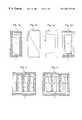
- FIG. 1 ais a diagrammatic view of a basic structure of a semiconductor component according to the invention.
- FIG. 1 bis a potential profile in the case of reverse voltage in the semiconductor component of FIG. 1 a;
- FIG. 1 cis a profile of the electric field in the case of reverse voltage in the semiconductor component of FIG. 1 a;
- FIG. 1 dis a diagrammatic view of a space charge distribution in the case of reverse voltage in the semiconductor component of FIG. 1 a;
- FIG. 2is a section taken through a first exemplary embodiment of the semiconductor component according to the invention with only approximately mutually compensating n- and p-conducting regions in the drift path,
- FIG. 3is a section take through a second exemplary embodiment of the semiconductor component according to the invention with only approximately mutually compensating n- and p-conducting regions in the drift path;
- FIG. 4is a section taken through a third exemplary embodiment of the semiconductor component according to the invention with a planar DMOS transistor having semi-insulating layers isolated from the semiconductor material by silicon dioxide;
- FIG. 5is a section taken through a fourth exemplary embodiment of the semiconductor component according to the invention with a planar DMOS transistor having approximately mutually compensating n- and p-conducting regions in the drift path;
- FIG. 6is a section taken through a fifth exemplary embodiment of the semiconductor component according to the invention with a Schottky diode having semi-insulating layers isolated from the semiconductor material by silicon dioxide;
- FIG. 7is a section taken through a sixth exemplary embodiment of the semiconductor component according to the invention with a Schottky diode having approximately mutually compensating n- and p-conducting regions in the drift path;
- FIG. 8is a section taken through a seventh exemplary embodiment of the semiconductor component according to the invention with a Schottky diode having approximately mutually compensating n- and p-conducting regions in the drift path and a filling of trenches etched during the fabrication with silicon dioxide.
- the componenthas a semiconductor body 1 made of an n+-conducting semiconductor substrate 2 , an n-conducting semiconductor layer 3 provided on the latter, a p-conducting semiconductor layer 4 , which forms a pn junction with the semiconductor layer 3 , electrodes 5 and 6 , and also semi-insulating layers made of SIPOS, for example.
- the semi-insulating layers 7extend between the two electrodes 5 , 6 on both sides of the pn junction.
- the semiconductor body 1may also comprise a p + -conducting semiconductor substrate 2 and a p-conducting semiconductor layer 3 , on which an n-conducting semiconductor layer 4 is then provided.
- a narrow strip of the pn junctionis provided with the semi-insulating layer 7 on one or alternatively (as illustrated) on both sides.
- a reverse voltageis applied between the electrodes 5 and 6 across the pn junction between the layers 3 and 4 , a small current flow through the semi-insulating layers 7 then leads to a linear rise in a potential P between the electrodes 5 , 6 as a function of a depth T, as is shown in FIG. 1 ( b ).
- the space charge zoneextends over the entire depth T of the n-conducting layer 3 , provided that the doping of this n-conducting layer 3 , integrated over the width thereof, does not exceed the breakdown charge, that is to say approximately 1 ⁇ 10 12 cm ⁇ 2 in the case of silicon.
- the countercharges to the ionized dopant atoms in the n-conducting layer 3are made available by the semi-insulating layers 7 , as is indicated diagrammatically in FIG. 1 ( d ).
- the doping of the n-conducting layer 3integrated over the depth T of the n-conducting layer 3 , to exceed the breakdown charge by a multiple without adversely affecting the blocking ability of the pn junction with respect to the layer 4 .
- FIGS. 2 to 8Various concrete exemplary embodiments of the semiconductor component according to the invention will now be explained with reference to FIGS. 2 to 8 .
- FIG. 2shows a first exemplary embodiment, in which, in addition to the basic structure of FIG. 1, p-conducting “pillars” 8 are also provided and the semi-insulating layers 7 made of SIPOS already terminate at the n + -conducting silicon semiconductor substrate 2 .
- p-conducting pillars 8provide the majority of the electric charge required for compensation purposes, with the result that the exact compensation can be ensured by the additional semi-insulating layers 7 .
- FIG. 3shows a modification of the exemplary embodiment of FIG. 2, where a plurality of p-conducting pillars 8 are respectively inserted between semi-insulating layers 7 in this case.
- One essential advantage of the semiconductor component according to the inventionis that it is possible to avoid accurately setting the doping in the p-conducting pillars 8 for compensation of the charges owing to the fact that this compensation of the charges is effected by means of the semi-insulating layers 7 , which provide the required charges in a self-aligned manner as a result of the linear resistive voltage drop.
- FIGS. 4 and 5show two further exemplary embodiments of the semiconductor component according to the invention with reference to a vertical DMOS field-effect transistor having a planar gate electrode 9 , a source or body electrode 10 , an n + -conducting source zone 11 , a p-conducting body or channel region 12 and insulating layers 13 which are each composed of silicon dioxide and/or silicon nitride and are provided between the n-conducting semiconductor layers 3 and the semi-insulating layers 7 .
- FIG. 5shows an exemplary embodiment which is modified with respect to that of FIG. 4, where, instead of the insulating layers 13 , the so-called “composite buffer layer” technique with p-conducting pillars 8 is again employed in this case.
- the gate electrodes 9are embedded in a customary manner in an insulating layer made, for example, of silicon dioxide and/or silicon nitride.
- an insulating layermade, for example, of silicon dioxide and/or silicon nitride.
- polycrystalline siliconcan be used for the gate electrodes 9
- the source electrodes 10 and the drain electrode 6may be composed of aluminum for example.
- FIGS. 6 to 8show further exemplary embodiments of the semiconductor component according to the invention with reference to a Schottky diode, in which the electrodes 15 form a Schottky contact on the anode side with the n-conducting semiconductor layer 3 and, in a similar manner to that in the exemplary embodiment of FIG. 4, insulating layers 13 are provided between the semi-insulating layers 7 and the semiconductor layers 3 .
- FIG. 7shows a modification of the exemplary embodiment of FIG. 6, where in this case, in a similar manner to that in the exemplary embodiment of FIG. 5 but now in the case of a Schottky diode -,p-conducting pillars 8 are additionally present for compensation purposes.
- an insulating layer 14 made of silicon dioxide, for example,is additionally “filled” into a semi-insulating layer 7 .
- Such a configurationmay be advantageous if relatively wide trenches are introduced into the n-conducting semiconductor layer 3 in order first of all to produce the p-conducting pillars from said trenches by means of diffusion and then to fill these trenches with SIPOS, for example, at their edge. The remainder of the trenches can be closed by means of silicon dioxide 14 , for example.
- the present inventioncan readily be applied to lateral structures as well.
- the insulating layers 13 surrounding the semi-insulating layers 7can, if appropriate, also be omitted.
- the semi-insulating layers 7can be produced in a relatively simple manner.
- SIPOScan be deposited in a similar manner to polycrystalline silicon.
- Preferred layer thicknesseslie in the range from 1 to 10 ⁇ m for the n-conducting layers, while the semi-insulating layers 7 , likewise in the same direction, may have a layer thickness of from 0.1 to 2 ⁇ m.
- the resistivity of the semi-insulating layersshould be in the region of approximately 1 ⁇ 10 10 ohm cm, although values vastly different from this are also possible. Resistivity values in the range from 10 8 to 10 11 ohms cm are at any rate suitable.
Landscapes
- Metal-Oxide And Bipolar Metal-Oxide Semiconductor Integrated Circuits (AREA)
- Insulated Gate Type Field-Effect Transistor (AREA)
Abstract
Description
Field of the Invention
The invention lies in the semiconductor technology field. More specifically, the present invention relates to a semiconductor component having a small forward voltage and a high blocking ability, in which at least one drift path suitable for taking up voltage is formed in a semiconductor body between two mutually spaced-apart electrodes.
Power MOS field-effect transistors should inherently have, on the one hand, a predetermined minimum breakdown voltage, but on the other hand the highest possible conductance with regard to the area of a semiconductor body that is used for them (“silicon area”). However, the minimum breakdown voltage and the conductance are coupled with one another in the case of customary semiconductor components: high conductivity is only obtained by a high doping and/or a small thickness or drift path length, which leads, however, to a low breakdown voltage and hence to a low blocking ability. In other words, a relatively high breakdown voltage and at the same time a high conductance cannot be achieved with conventional semiconductor components. This also applies to other unipolar semiconductor components such as, for example, Schottky diodes (in this context, see B. J. Baliga: “Modern Power Devices”, John Wiley & Sons, 1987, in particular Equation 6.60, FIG. 6.23 and also pages 421 ff. and 132 ff.).
In addition to the power MOSFET disclosed above, various possibilities have already been conceived of with the aim of avoiding the problem of the coupling of breakdown voltage and conductivity, so that each of these two properties can be optimized in favor of itself.
In the first instance, there are semiconductor components known as IGBTs (insulated gate bipolar transistors), which are also referred to as IGT (insulated gate transistor) or as COMFET (conductivity modulated FET). In the case of such a semiconductor component, the inherently weakly doped drift path, that is to say the “central region” which has to take up the reverse voltage, is flooded, in the case of forward-biasing, with an electron-hole plasma having a considerably higher conductivity than the weak doping of the central region (cf. B. J. Baliga, pages 350-53).
Moreover, U.S. Pat. No. 4,941,026 discloses a semiconductor component in which the electric charge contained in the drift path doping is compensated for, in the case of reverse-biasing, by charges from a gate arranged in a deep trench. In the case of such a structure, the charge in the drift path contributes to the build-up of the vertical field strength between the two electrodes only is a greatly reduced manner and, therefore, can be chosen to be considerably higher compared with customary semiconductor components. Thus, by way of example, it is possible to introduce up to twice the breakdown charge as doping in a drift path region between two trenches.
Finally, consideration has also already been given for a relatively longtime to so-called compensation components, in the case of which compensation of the drift path charge in the case of reverse-biasing of the semiconductor component is provided by means of regions arranged parallel to the drift path or zones having an opposite doping to the drift path doping (in this respect, see U.S. Pat. No. 4,754,310 and U.S. Pat. No. 5,216,275). However, in the case of those prior art semiconductor components, too, the doping of the individual regions must not exceed twice the breakdown charge (2×10¹²charge carriers cm−2in the case of Si).
These so-called compensation components are based on mutual compensation of the charge of n- and p-doped regions in the drift path of a MOS transistor, for example. In this case, these regions are spatially arranged such that the line integral against the doping remains below the material-specific breakdown charge specified above, in other words below approximately 2×1012cm−2in the case of silicon. By way of example, in a vertical transistor of the kind that is customary in power electronics, p- and n-type “pillars” or “plates”, etc. may be arranged in pairs. In a lateral structure, p- and n-conducting layers may be stacked alternately one above the other laterally between a trench occupied by a p-conducting layer and a trench occupied by an n-conducting layer (cf. U.S. Pat. No. 4,754,310).
The aforementioned compensation components require relatively accurate setting of the dopant concentrations in the individual zones and regions in order to actually achieve the desired compensation. This setting of the dopant concentrations has proved to be relatively difficult if, in particular, doping is intended to be performed over a relatively long period of time on different semiconductor chips.
It is accordingly an object of the invention to provide a semiconductor component having a small forward voltage and a high blocking ability, which overcomes the above-mentioned disadvantages of the heretofore-known devices and methods of this general type and which, in terms of its functionality, is independent of the variations in the process parameters which are customary in semiconductor fabrication.
With the foregoing and other objects in view there is provided, in accordance with the invention, a semiconductor component having a small forward voltage and a high blocking ability, comprising:
two mutually spaced-apart electrodes;
a semiconductor body disposed between the two electrodes and defining therein at least one drift path suitable for taking up voltage; and
at least one semi-insulating layer extending parallel to the drift path.
In accordance with an added feature of the invention, the semiconductor body is of a first conductivity type and which further comprises regions of a second conductivity type, opposite the first conductivity type, formed in the semiconductor body and extending parallel to the semi-insulating layer.
Examples of material that can be used for the semi-insulating layer are semi-insulating polycrystalline silicon (SIPOS), amorphous silicon optionally doped with H (a-Si:H) or amorphous carbon optionally doped with hydrogen (a-C:H). It goes without saying that other materials having semi-insulating properties can also be used.
In accordance with a further feature of the invention, the semi-insulating layer has a defined resistivity in a range from 108to 1011ohms cm, forinstance 1×10¹⁰ohms cm.
Semi-insulating layers are known for other purposes in semiconductor technology: thus, by way of example, there are resistive field plates in the case of edge terminations with a high blocking capability which comprise SIPOS (cf. Baliga, pages 126 ff. and Jaume et al., “High-Voltage Planar Devices Using Field Plate and Semi-Resistive Layers,” IEEE Transactions on Electron Devices, Vol. 38, No. 7, pp. 1681-84 (1991)).
In accordance with again an added feature of the invention, the semiconductor body is formed with a pn junction having two sides, and the semi-insulating layer is disposed adjacent at least one of the two sides.
In accordance with again an additional feature of the invention, a doping in the drift path does not exceed a breakdown charge of the component. In an exemplary embodiment, the drift path is formed of silicon and the doping in the drift path does not exceed 1×10¹²charge carriers cm−2.
In the case of the semiconductor component according to the invention, by way of example, a narrow strip of a pn junction is provided with a semi-insulating layer on one or both sides. When a reverse voltage is applied to the pn junction, even a relatively low current flow through the semi-insulating layer then leads to a linear rise in the potential between the two electrodes and thus to an essentially constant electric field. In this case, the space charge zone extends over the entire depth of the drift path. However, the doping in the drift path, that is to say an n-conducting semiconductor region for example, integrated over the width of the drift path, must not exceed the breakdown charge, approximately 1×10¹²charge carriers cm−2in silicon. For two semi-insulating layers which bound a drift path, twice the specified value for the breakdown charge correspondingly applies. In the above-mentioned preferred embodiment, that breakdown charge thus does note exceed 2×10¹²charge carriers per square centimeter.
In the case of the semiconductor component according to the invention, countercharges to the ionized dopant atoms in the drift path are made available by the semi-insulating layer. As a result, the doping of the drift path, integrated over the depth of the drift path, can exceed the breakdown charge by a multiple without adversely affecting the blocking ability of the pn junction.
In accordance with again another feature of the invention, the semi-insulating layer is arranged between the two electrodes.
In accordance with yet a further feature of the invention, the semiconductor body is n-doped.
In accordance with a preferred embodiment of the invention, regions of a second conductivity type are provided parallel to the semi-insulating layer in a semiconductor body of the first conductivity type, opposite the second conductivity type. In other words, the compensation of the above-mentioned drift path charge is employed, in which case, however, the compensation of the charges is automatically established by way of the current flow in the semi-insulating layer in the case of the semiconductor component according to the invention, which considerably reduces the requirements imposed on the accuracy of the doping concentration in the individual layers.
In other words, by virtue of the so-called “composite buffer layer” technique, in which, by way of example, p-conducting “pillars” are embedded in an n-conducting semiconductor region of a drift path, the majority of the charge required for compensation purposes can be made available in these p-conducting pillars. The exact compensation is then effected, however, by the additional semi-insulating layers.
Such a procedure affords particular advantages: on the one hand, the high accuracy is not required in the case of the doping of the p-conducting pillars; on the other hand, however, the countercharge required in the semi-insulating layers is small, which makes the charge-reversal current flowing during switching operations in the semi-insulating layer small and reduces the charge-reversal time.
In accordance with a concomitant feature of the invention, there are provided a multiplicity of mutually parallel drift paths in the semiconductor body.
The semiconductor component according to the invention may advantageously be a power MOSFET such as, by way of example, a planar DMOS field-effect transistor or a trench DMOS field-effect transistor, a Schottky diode, a junction field-effect transistor (JFET), etc.
Other features which are considered as characteristic for the invention are set forth in the appended claims.
Although the invention is illustrated and described herein as embodied in a semiconductor component having a small forward voltage and a high blocking ability, it is nevertheless not intended to be limited to the details shown, since various modifications and structural changes may be made therein without departing from the spirit of the invention and within the scope and range of equivalents of the claims.
The construction and method of operation of the invention, however, together with additional objects and advantages thereof will be best understood from the following description of specific embodiments when read in connection with the accompanying drawings.
FIG. 1ais a diagrammatic view of a basic structure of a semiconductor component according to the invention;
FIG. 1bis a potential profile in the case of reverse voltage in the semiconductor component of FIG. 1a;
FIG. 1cis a profile of the electric field in the case of reverse voltage in the semiconductor component of FIG. 1a;
FIG. 1dis a diagrammatic view of a space charge distribution in the case of reverse voltage in the semiconductor component of FIG. 1a;
FIG. 2 is a section taken through a first exemplary embodiment of the semiconductor component according to the invention with only approximately mutually compensating n- and p-conducting regions in the drift path,
FIG. 3 is a section take through a second exemplary embodiment of the semiconductor component according to the invention with only approximately mutually compensating n- and p-conducting regions in the drift path;
FIG. 4 is a section taken through a third exemplary embodiment of the semiconductor component according to the invention with a planar DMOS transistor having semi-insulating layers isolated from the semiconductor material by silicon dioxide;
FIG. 5 is a section taken through a fourth exemplary embodiment of the semiconductor component according to the invention with a planar DMOS transistor having approximately mutually compensating n- and p-conducting regions in the drift path;
FIG. 6 is a section taken through a fifth exemplary embodiment of the semiconductor component according to the invention with a Schottky diode having semi-insulating layers isolated from the semiconductor material by silicon dioxide;
FIG. 7 is a section taken through a sixth exemplary embodiment of the semiconductor component according to the invention with a Schottky diode having approximately mutually compensating n- and p-conducting regions in the drift path; and
FIG. 8 is a section taken through a seventh exemplary embodiment of the semiconductor component according to the invention with a Schottky diode having approximately mutually compensating n- and p-conducting regions in the drift path and a filling of trenches etched during the fabrication with silicon dioxide.
Mutually corresponding structural parts are each identified with the same reference symbols throughout the figures. Moreover, in the figures that show sectional illustrations (FIG. 1a,FIG. 1b,and FIGS. 2 to8), not all the sectioned surfaces are hatched, in order to afford better clarity.
Referring now to the figures of the drawing in detail and first, particularly, to FIG. 1athereof, there is seen a basic structure of the semiconductor component according to the invention. The component has asemiconductor body 1 made of an n+-conductingsemiconductor substrate 2, an n-conductingsemiconductor layer 3 provided on the latter, a p-conductingsemiconductor layer 4, which forms a pn junction with thesemiconductor layer 3,electrodes electrodes
It shall be noted that in this example, as in the following exemplary embodiments, the conductivity types can also be reversed in each case. In other words, thesemiconductor body 1 may also comprise a p+-conductingsemiconductor substrate 2 and a p-conductingsemiconductor layer 3, on which an n-conductingsemiconductor layer 4 is then provided.
In the case of the semiconductor component according to the invention, then, a narrow strip of the pn junction is provided with thesemi-insulating layer 7 on one or alternatively (as illustrated) on both sides. When a reverse voltage is applied between theelectrodes layers semi-insulating layers 7 then leads to a linear rise in a potential P between theelectrodes
In this case, the space charge zone extends over the entire depth T of the n-conductinglayer 3, provided that the doping of this n-conductinglayer 3, integrated over the width thereof, does not exceed the breakdown charge, that is to say approximately 1×1012cm−2in the case of silicon. In this case, the countercharges to the ionized dopant atoms in the n-conductinglayer 3 are made available by thesemi-insulating layers 7, as is indicated diagrammatically in FIG.1(d).
Thus, it is possible for the doping of the n-conductinglayer 3, integrated over the depth T of the n-conductinglayer 3, to exceed the breakdown charge by a multiple without adversely affecting the blocking ability of the pn junction with respect to thelayer 4.
Various concrete exemplary embodiments of the semiconductor component according to the invention will now be explained with reference to FIGS. 2 to8.
FIG. 2 shows a first exemplary embodiment, in which, in addition to the basic structure of FIG. 1, p-conducting “pillars”8 are also provided and thesemi-insulating layers 7 made of SIPOS already terminate at the n+-conductingsilicon semiconductor substrate 2. These p-conductingpillars 8 provide the majority of the electric charge required for compensation purposes, with the result that the exact compensation can be ensured by the additional semi-insulating layers7. As a result of this, on the one hand, a high accuracy is not required in the doping of the p-conductingpillars 8, and, on the other hand, the countercharge required in thesemi-insulating layers 7 is small, which leads to a reduction in the space charge current flowing during switching operations in thesemi-insulating layers 7 and hence to a reduction in the charge-reversal time.
FIG. 3 shows a modification of the exemplary embodiment of FIG. 2, where a plurality of p-conductingpillars 8 are respectively inserted betweensemi-insulating layers 7 in this case.
One essential advantage of the semiconductor component according to the invention is that it is possible to avoid accurately setting the doping in the p-conductingpillars 8 for compensation of the charges owing to the fact that this compensation of the charges is effected by means of thesemi-insulating layers 7, which provide the required charges in a self-aligned manner as a result of the linear resistive voltage drop.
FIGS. 4 and 5 show two further exemplary embodiments of the semiconductor component according to the invention with reference to a vertical DMOS field-effect transistor having aplanar gate electrode 9, a source orbody electrode 10, an n+-conductingsource zone 11, a p-conducting body orchannel region 12 and insulatinglayers 13 which are each composed of silicon dioxide and/or silicon nitride and are provided between the n-conductingsemiconductor layers 3 and the semi-insulating layers7. What is essential, however, is that in the exemplary embodiment of FIG. 4, there is contact between thesemi-insulating layers 7 and the respective layers or electrodes that are at reverse-biasing potential, that is to say thesource electrode 10 and respectively, via the n+-conductingsilicon semiconductor substrate 2, thedrain electrode 6.
FIG. 5 shows an exemplary embodiment which is modified with respect to that of FIG. 4, where, instead of the insulatinglayers 13, the so-called “composite buffer layer” technique with p-conductingpillars 8 is again employed in this case.
It shall also be noted that in the exemplary embodiments of FIGS. 4 and 5, thegate electrodes 9 are embedded in a customary manner in an insulating layer made, for example, of silicon dioxide and/or silicon nitride. By way of example, polycrystalline silicon can be used for thegate electrodes 9, while thesource electrodes 10 and thedrain electrode 6 may be composed of aluminum for example.
FIGS. 6 to8 show further exemplary embodiments of the semiconductor component according to the invention with reference to a Schottky diode, in which the electrodes15 form a Schottky contact on the anode side with the n-conductingsemiconductor layer 3 and, in a similar manner to that in the exemplary embodiment of FIG. 4, insulatinglayers 13 are provided between thesemi-insulating layers 7 and the semiconductor layers3.
FIG. 7 shows a modification of the exemplary embodiment of FIG. 6, where in this case, in a similar manner to that in the exemplary embodiment of FIG. 5 but now in the case of a Schottky diode -,p-conductingpillars 8 are additionally present for compensation purposes.
In the exemplary embodiment of FIG. 8, in contrast to the exemplary embodiment of FIG. 7, an insulatinglayer 14 made of silicon dioxide, for example, is additionally “filled” into asemi-insulating layer 7. Such a configuration may be advantageous if relatively wide trenches are introduced into the n-conductingsemiconductor layer 3 in order first of all to produce the p-conducting pillars from said trenches by means of diffusion and then to fill these trenches with SIPOS, for example, at their edge. The remainder of the trenches can be closed by means ofsilicon dioxide 14, for example.
Although exemplary embodiments configured in a vertical structure have been explained, the present invention can readily be applied to lateral structures as well. Moreover, as has already been mentioned, instead of the preferably used SIPOS, it is also possible to use a different semi-insulating material. The insulating layers13 surrounding thesemi-insulating layers 7 can, if appropriate, also be omitted.
The semi-insulating layers7 can be produced in a relatively simple manner. By way of example, SIPOS can be deposited in a similar manner to polycrystalline silicon.
Preferred layer thicknesses (that is to say, for example, from “left” to “right” in FIG.1(a) lie in the range from 1 to 10 μm for the n-conducting layers, while thesemi-insulating layers 7, likewise in the same direction, may have a layer thickness of from 0.1 to 2 μm.
The resistivity of the semi-insulating layers should be in the region of approximately 1×10¹⁰ohm cm, although values vastly different from this are also possible. Resistivity values in the range from 108to 1011ohms cm are at any rate suitable.
Claims (16)
1. A semiconductor component having a small forward voltage and a high blocking ability, comprising:
two mutually spaced-apart electrodes;
a semiconductor body disposed between said two electrodes and defining therein at least one drift path suitable for taking up voltage; and
at least one semi-insulating layer extending parallel to said drift path.
2. The semiconductor component according to claim1, wherein said semiconductor body is of a first conductivity type and which further comprises regions of a second conductivity type, opposite the first conductivity type, formed in said semiconductor body and extending parallel to said semi-insulating layer.
3. The semiconductor component according to claim1, wherein said semi-insulating layer is composed of a material selected from the group consisting of semi-insulating polycrystalline silicon, amorphous silicon, and amorphous carbon.
4. The semiconductor component according to claim1, wherein said semi-insulating layer is composed of a material selected from the group consisting of amorphous silicon and amorphous carbon doped with hydrogen.
5. The semiconductor component according to claim1, wherein said semi-insulating layer has a defined resistivity in a range from 108to 1011ohms cm.
6. The semiconductor component according to claim1, wherein said semiconductor body is formed with a pn junction having two sides, and said semi-insulating layer is disposed adjacent at least one of said two sides.
7. The semiconductor component according to claim1, wherein a doping in said drift path does not exceed a breakdown charge of the component.
8. The semiconductor component according to claim7, wherein said drift path is formed of silicon and the doping in said drift path does not exceed 1×10¹²charge carriers cm−2.
9. The semiconductor component according to claim1, wherein the at least one semi-insulating layer is one of two semi-insulating layers disposed on both sides of said semiconductor body, and a doping in said drift path does not exceed twice a breakdown charge.
10. The semiconductor component according to claim9, wherein said drift path is formed of silicon and the doping in said drift path does not exceed 2×10¹²charge carriers cm−2.
11. The semiconductor component according to claim1, wherein said semi-insulating layer is arranged between said two electrodes.
12. The semiconductor component according to claim1, wherein said semiconductor body is n-doped.
13. The semiconductor component according to claim1, wherein said drift path is one of a multiplicity of mutually parallel drift paths formed in said semiconductor body.
14. The semiconductor component according to claim1, wherein said electrodes, said semiconductor body, and said semi-insulating layer define a power MOSFET.
15. The semiconductor component according to claim1, wherein said electrodes, said semiconductor body, and said semi-insulating layer define a Schottky diode.
16. The semiconductor component according to claim1, wherein said electrodes, said semiconductor body, and said semi-insulating layer define a junction field-effect transistor.
Applications Claiming Priority (2)
| Application Number | Priority Date | Filing Date | Title |
|---|---|---|---|
| DE19848828 | 1998-10-22 | ||
| DE19848828ADE19848828C2 (en) | 1998-10-22 | 1998-10-22 | Semiconductor device with low forward voltage and high blocking capability |
Publications (1)
| Publication Number | Publication Date |
|---|---|
| US6201279B1true US6201279B1 (en) | 2001-03-13 |
Family
ID=7885359
Family Applications (1)
| Application Number | Title | Priority Date | Filing Date |
|---|---|---|---|
| US09/425,340Expired - LifetimeUS6201279B1 (en) | 1998-10-22 | 1999-10-22 | Semiconductor component having a small forward voltage and high blocking ability |
Country Status (2)
| Country | Link |
|---|---|
| US (1) | US6201279B1 (en) |
| DE (1) | DE19848828C2 (en) |
Cited By (73)
| Publication number | Priority date | Publication date | Assignee | Title |
|---|---|---|---|---|
| US20020175351A1 (en)* | 2001-04-11 | 2002-11-28 | Baliga Bantval Jayant | Power semiconductor devices having retrograded-doped transition regions that enhance breakdown voltage characteristics and methods of forming same |
| US20020185679A1 (en)* | 2000-06-23 | 2002-12-12 | Baliga Bantval Jayant | Power semiconductor devices having linear transfer characteristics and methods of forming and operating same |
| WO2003015178A1 (en)* | 2001-08-07 | 2003-02-20 | Koninklijke Philips Electronics N.V. | Trench bipolar transistor |
| WO2003034470A3 (en)* | 2001-10-17 | 2003-09-12 | Fairchild Semiconductor | Semiconductor structure with improved smaller forward voltage loss and higher blocking capability |
| US20030173624A1 (en)* | 2002-02-23 | 2003-09-18 | Fairchild Korea Semiconductor Ltd. | High breakdown voltage low on-resistance lateral DMOS transistor |
| US6624472B2 (en)* | 2000-02-12 | 2003-09-23 | Koninklijke Philips Electronics N.V. | Semiconductor device with voltage sustaining zone |
| WO2003085722A3 (en)* | 2002-03-29 | 2003-11-27 | Fairchild Semiconductor | Field effect transistor having a lateral depletion structure |
| US20040021173A1 (en)* | 2002-07-30 | 2004-02-05 | Fairchild Semiconductor Corporation | Dual trench power mosfet |
| US6690085B2 (en)* | 2001-07-17 | 2004-02-10 | Kabushiki Kaisha Toshiba | High-voltage semiconductor device used as switching element or the like |
| US6700175B1 (en)* | 1999-07-02 | 2004-03-02 | Kabushiki Kaisha Toyota Chuo Kenkyusho | Vertical semiconductor device having alternating conductivity semiconductor regions |
| US20040043565A1 (en)* | 2002-04-01 | 2004-03-04 | Masakazu Yamaguchi | Semiconductor device and method of manufacturing the same |
| US6710418B1 (en) | 2002-10-11 | 2004-03-23 | Fairchild Semiconductor Corporation | Schottky rectifier with insulation-filled trenches and method of forming the same |
| US6713813B2 (en) | 2001-01-30 | 2004-03-30 | Fairchild Semiconductor Corporation | Field effect transistor having a lateral depletion structure |
| US20040065919A1 (en)* | 2002-10-03 | 2004-04-08 | Wilson Peter H. | Trench gate laterally diffused MOSFET devices and methods for making such devices |
| US20040099905A1 (en)* | 2001-04-11 | 2004-05-27 | Baliga Bantval Jayant | Power semiconductor devices having laterally extending base shielding regions that inhibit base reach-through and schottky rectifying flyback diodes |
| US20040115790A1 (en)* | 2001-02-13 | 2004-06-17 | Tiina Pakula | Method for production of secreted proteins in fungi |
| JP2004519103A (en)* | 2001-02-15 | 2004-06-24 | コーニンクレッカ フィリップス エレクトロニクス エヌ ヴィ | Semiconductor devices and their peripheral terminal processing |
| US20040132252A1 (en)* | 2001-01-30 | 2004-07-08 | Merchant Bruce D. | Method of forming a field effect transistor having a lateral depletion structure |
| US20040142523A1 (en)* | 2000-08-16 | 2004-07-22 | Izak Bencuya | Method of forming vertical mosfet with ultra-low on-resistance and low gate charge |
| DE10258467B3 (en)* | 2002-12-13 | 2004-09-30 | Infineon Technologies Ag | Power semiconductor component used as a power transistor has a field electrode formed in the lower region of the trenches away from the upper surface of the semiconductor body |
| US6803626B2 (en) | 2002-07-18 | 2004-10-12 | Fairchild Semiconductor Corporation | Vertical charge control semiconductor device |
| DE10317383A1 (en)* | 2003-04-15 | 2004-11-11 | Infineon Technologies Ag | Junction field effect transistor (JFET) for providing fast switch with low switch-on resistance comprising compensator in form of field plate |
| US20040232407A1 (en)* | 1999-12-20 | 2004-11-25 | Fairchild Semiconductor Corporation | Power MOS device with improved gate charge performance |
| US20040232481A1 (en)* | 2003-05-20 | 2004-11-25 | Robert Herrick | Structure and method for forming a trench MOSFET having self-aligned features |
| US20040256690A1 (en)* | 2001-10-17 | 2004-12-23 | Kocon Christopher Boguslaw | Schottky diode using charge balance structure |
| US20050012121A1 (en)* | 2003-05-12 | 2005-01-20 | Infineon Technologies Ag | Semiconductor component |
| US20050116313A1 (en)* | 2003-11-28 | 2005-06-02 | Lee Jae-Gil | Superjunction semiconductor device |
| US20050121691A1 (en)* | 2003-12-05 | 2005-06-09 | Jean-Luc Morand | Active semiconductor component with a reduced surface area |
| US20050153497A1 (en)* | 2000-08-16 | 2005-07-14 | Izak Bencuya | Method of forming a FET having ultra-low on-resistance and low gate charge |
| US20050167742A1 (en)* | 2001-01-30 | 2005-08-04 | Fairchild Semiconductor Corp. | Power semiconductor devices and methods of manufacture |
| US20050199918A1 (en)* | 2004-03-15 | 2005-09-15 | Daniel Calafut | Optimized trench power MOSFET with integrated schottky diode |
| US20060011962A1 (en)* | 2003-12-30 | 2006-01-19 | Kocon Christopher B | Accumulation device with charge balance structure and method of forming the same |
| WO2005078802A3 (en)* | 2004-02-13 | 2006-02-02 | Infineon Technologies Ag | High-blocking semiconductor component comprising a drift section |
| US20060030142A1 (en)* | 2004-08-03 | 2006-02-09 | Grebs Thomas E | Semiconductor power device having a top-side drain using a sinker trench |
| US20060065923A1 (en)* | 2004-09-24 | 2006-03-30 | Infineon Technologies Ag. | High-voltage-resistant semiconductor component having vertically conductive semiconductor body areas and a trench structure |
| US20060076617A1 (en)* | 2004-10-08 | 2006-04-13 | Shenoy Praveen M | MOS-gated transistor with reduced miller capacitance |
| US20060141684A1 (en)* | 2004-12-24 | 2006-06-29 | Au Optronics Corp. | Polysilicon film, thin film transistor using the same, and method for forming the same |
| US7078296B2 (en) | 2002-01-16 | 2006-07-18 | Fairchild Semiconductor Corporation | Self-aligned trench MOSFETs and methods for making the same |
| US20060214221A1 (en)* | 2003-05-20 | 2006-09-28 | Ashok Challa | Power semiconductor devices and methods of manufacture |
| US7132712B2 (en) | 2002-11-05 | 2006-11-07 | Fairchild Semiconductor Corporation | Trench structure having one or more diodes embedded therein adjacent a PN junction |
| US20060249788A1 (en)* | 2000-06-02 | 2006-11-09 | Blanchard Richard A | High voltage power MOSFET having low on-resistance |
| US20060267090A1 (en)* | 2005-04-06 | 2006-11-30 | Steven Sapp | Trenched-gate field effect transistors and methods of forming the same |
| US20070054439A1 (en)* | 2005-07-14 | 2007-03-08 | Siliconware Precision Industries Co., Ltd. | Multi-chip stack structure |
| US20070249142A1 (en)* | 2006-04-19 | 2007-10-25 | Toyota Jidosha Kabushiki Kaisha | Semiconductor devices and method of manufacturing them |
| US7319256B1 (en) | 2006-06-19 | 2008-01-15 | Fairchild Semiconductor Corporation | Shielded gate trench FET with the shield and gate electrodes being connected together |
| US20080090339A1 (en)* | 2005-08-09 | 2008-04-17 | Robert Herrick | Method for Forming Inter-Poly Dielectric in Shielded Gate Field Effect Transistor |
| US20080111207A1 (en)* | 2006-11-15 | 2008-05-15 | Lee Jae-Gil | High-Voltage Semiconductor Device and Method of Fabricating the Same |
| EP1583152A3 (en)* | 2004-03-11 | 2008-08-06 | Yokogawa Electric Corporation | Semiconductor device with lightly doped layer and method of manufacturing the same |
| US7446374B2 (en) | 2006-03-24 | 2008-11-04 | Fairchild Semiconductor Corporation | High density trench FET with integrated Schottky diode and method of manufacture |
| US20090079002A1 (en)* | 2007-09-21 | 2009-03-26 | Jaegil Lee | Superjunction Structures for Power Devices and Methods of Manufacture |
| KR100900852B1 (en) | 2001-02-22 | 2009-06-04 | 엔엑스피 비 브이 | Semiconductor devices |
| US20090166728A1 (en)* | 2007-12-26 | 2009-07-02 | James Pan | Structure and Method for Forming Shielded Gate Trench FET with Multiple Channels |
| US20090189216A1 (en)* | 2008-01-25 | 2009-07-30 | Infineon Technologies Austria Ag | Semiconductor component including a drift zone and a drift control zone |
| US7576388B1 (en) | 2002-10-03 | 2009-08-18 | Fairchild Semiconductor Corporation | Trench-gate LDMOS structures |
| US20090218621A1 (en)* | 2005-07-27 | 2009-09-03 | Infineon Technologies Austria Ag | Semiconductor component with a drift region and a drift control region |
| US20090315020A1 (en)* | 2008-06-18 | 2009-12-24 | Sandhu Gurtej S | Diodes, and Methods of Forming Diodes |
| US8110868B2 (en) | 2005-07-27 | 2012-02-07 | Infineon Technologies Austria Ag | Power semiconductor component with a low on-state resistance |
| US8319290B2 (en) | 2010-06-18 | 2012-11-27 | Fairchild Semiconductor Corporation | Trench MOS barrier schottky rectifier with a planar surface using CMP techniques |
| CN103137684A (en)* | 2011-11-21 | 2013-06-05 | 朱江 | Super junction structure semiconductor wafer with insulating layer isolation and preparation method thereof |
| CN103208533A (en)* | 2012-01-13 | 2013-07-17 | 朱江 | Schottky super junction semiconductor device and preparation method thereof |
| CN103383968A (en)* | 2012-05-06 | 2013-11-06 | 朱江 | Interface charge compensation Schottky semiconductor device and manufacturing method for same |
| CN103594493A (en)* | 2012-08-15 | 2014-02-19 | 朱江 | Trench-structure charge compensation Schottky semiconductor device and preparation method thereof |
| CN103594494A (en)* | 2012-08-16 | 2014-02-19 | 朱江 | Charge-compensation schottky semiconductor device and manufacturing method thereof |
| US8673700B2 (en) | 2011-04-27 | 2014-03-18 | Fairchild Semiconductor Corporation | Superjunction structures for power devices and methods of manufacture |
| US8772868B2 (en) | 2011-04-27 | 2014-07-08 | Fairchild Semiconductor Corporation | Superjunction structures for power devices and methods of manufacture |
| US8786010B2 (en) | 2011-04-27 | 2014-07-22 | Fairchild Semiconductor Corporation | Superjunction structures for power devices and methods of manufacture |
| CN103943666A (en)* | 2013-01-17 | 2014-07-23 | 朱江 | Grooved semiconductor device and manufacturing method thereof |
| US20140231904A1 (en)* | 2013-02-18 | 2014-08-21 | Infineon Technologies Austria Ag | Super Junction Semiconductor Device with Overcompensation Zones |
| US8836028B2 (en) | 2011-04-27 | 2014-09-16 | Fairchild Semiconductor Corporation | Superjunction structures for power devices and methods of manufacture |
| US8884342B2 (en)* | 2012-08-29 | 2014-11-11 | Infineon Technologies Ag | Semiconductor device with a passivation layer |
| US8963212B2 (en) | 2008-12-08 | 2015-02-24 | Fairchild Semiconductor Corporation | Trench-based power semiconductor devices with increased breakdown voltage characteristics |
| US9431481B2 (en) | 2008-09-19 | 2016-08-30 | Fairchild Semiconductor Corporation | Superjunction structures for power devices and methods of manufacture |
| US11257900B2 (en)* | 2014-09-17 | 2022-02-22 | Fuji Electric Co., Ltd. | Semiconductor device |
Families Citing this family (11)
| Publication number | Priority date | Publication date | Assignee | Title |
|---|---|---|---|---|
| JP3971062B2 (en)* | 1999-07-29 | 2007-09-05 | 株式会社東芝 | High voltage semiconductor device |
| DE19945432A1 (en)* | 1999-09-22 | 2001-04-12 | Infineon Technologies Ag | EMV-type circuit arrangement for operating load |
| GB0003184D0 (en)* | 2000-02-12 | 2000-04-05 | Koninkl Philips Electronics Nv | A semiconductor device and a method of fabricating material for a semiconductor device |
| GB0003185D0 (en) | 2000-02-12 | 2000-04-05 | Koninkl Philips Electronics Nv | An insulated gate field effect device |
| JP4528460B2 (en) | 2000-06-30 | 2010-08-18 | 株式会社東芝 | Semiconductor element |
| DE10117802A1 (en)* | 2001-04-10 | 2002-10-24 | Bosch Gmbh Robert | Semiconductor power component e.g. emitter switched thyristor as ignition transistor of ignition coil of combustion engine, has drift zone joined to rear face emitter zone |
| DE102004005775B4 (en)* | 2004-02-05 | 2009-10-22 | Infineon Technologies Ag | Semiconductor device |
| DE102005011967B4 (en)* | 2005-03-14 | 2007-07-19 | Infineon Technologies Ag | Semiconductor device with drift path and trench structure and method for producing the same |
| DE102005035699B4 (en)* | 2005-07-27 | 2010-09-16 | Infineon Technologies Austria Ag | Semiconductor power device with charge compensation structure and method of making the same |
| DE102005048447B4 (en)* | 2005-10-07 | 2007-07-19 | Infineon Technologies Ag | Semiconductor power device with charge compensation structure and method of making the same |
| US8809949B2 (en) | 2009-06-17 | 2014-08-19 | Infineon Technologies Austria Ag | Transistor component having an amorphous channel control layer |
Citations (5)
| Publication number | Priority date | Publication date | Assignee | Title |
|---|---|---|---|---|
| US4754310A (en) | 1980-12-10 | 1988-06-28 | U.S. Philips Corp. | High voltage semiconductor device |
| US4941026A (en) | 1986-12-05 | 1990-07-10 | General Electric Company | Semiconductor devices exhibiting minimum on-resistance |
| US5216275A (en) | 1991-03-19 | 1993-06-01 | University Of Electronic Science And Technology Of China | Semiconductor power devices with alternating conductivity type high-voltage breakdown regions |
| US5723891A (en)* | 1992-05-18 | 1998-03-03 | Texas Instruments Incorporated | Top-drain trench based resurf DMOS transistor structure |
| US5780898A (en)* | 1994-08-25 | 1998-07-14 | Matsushita Electric Industrial Co. Ltd. | Semiconductor device with a vertical field effect transistor and method of manufacturing the same |
Family Cites Families (3)
| Publication number | Priority date | Publication date | Assignee | Title |
|---|---|---|---|---|
| US5637908A (en)* | 1994-09-28 | 1997-06-10 | Harris Corporation | Structure and technique for tailoring effective resistivity of a SIPOS layer by patterning and control of dopant introduction |
| WO1996019833A1 (en)* | 1994-12-20 | 1996-06-27 | Francis John Clough | High voltage thin film semiconductor device |
| GB2330452A (en)* | 1997-10-16 | 1999-04-21 | Plessey Semiconductors Ltd | Arrangement for inhibiting dielectric polarisation in high voltage devices |
- 1998
- 1998-10-22DEDE19848828Apatent/DE19848828C2/ennot_activeExpired - Fee Related
- 1999
- 1999-10-22USUS09/425,340patent/US6201279B1/ennot_activeExpired - Lifetime
Patent Citations (5)
| Publication number | Priority date | Publication date | Assignee | Title |
|---|---|---|---|---|
| US4754310A (en) | 1980-12-10 | 1988-06-28 | U.S. Philips Corp. | High voltage semiconductor device |
| US4941026A (en) | 1986-12-05 | 1990-07-10 | General Electric Company | Semiconductor devices exhibiting minimum on-resistance |
| US5216275A (en) | 1991-03-19 | 1993-06-01 | University Of Electronic Science And Technology Of China | Semiconductor power devices with alternating conductivity type high-voltage breakdown regions |
| US5723891A (en)* | 1992-05-18 | 1998-03-03 | Texas Instruments Incorporated | Top-drain trench based resurf DMOS transistor structure |
| US5780898A (en)* | 1994-08-25 | 1998-07-14 | Matsushita Electric Industrial Co. Ltd. | Semiconductor device with a vertical field effect transistor and method of manufacturing the same |
Non-Patent Citations (2)
| Title |
|---|
| B. Jayant Balagi: "Modern Power Devices", John Wiley & Sons, 1987. |
| D. Jaume et al.: "High-Voltage Planar Devices Using Field Plate and Semi-Restrictive Layers", IEEE Transactions On Electron devices, vol. 38, No. 7, Jul. 1991, pp. 1681-1684. |
Cited By (205)
| Publication number | Priority date | Publication date | Assignee | Title |
|---|---|---|---|---|
| US6700175B1 (en)* | 1999-07-02 | 2004-03-02 | Kabushiki Kaisha Toyota Chuo Kenkyusho | Vertical semiconductor device having alternating conductivity semiconductor regions |
| US7625793B2 (en) | 1999-12-20 | 2009-12-01 | Fairchild Semiconductor Corporation | Power MOS device with improved gate charge performance |
| US20040232407A1 (en)* | 1999-12-20 | 2004-11-25 | Fairchild Semiconductor Corporation | Power MOS device with improved gate charge performance |
| US20060024890A1 (en)* | 1999-12-20 | 2006-02-02 | Calafut Daniel S | Power MOS device with improved gate charge performance |
| US6624472B2 (en)* | 2000-02-12 | 2003-09-23 | Koninklijke Philips Electronics N.V. | Semiconductor device with voltage sustaining zone |
| US20060249788A1 (en)* | 2000-06-02 | 2006-11-09 | Blanchard Richard A | High voltage power MOSFET having low on-resistance |
| US7745885B2 (en)* | 2000-06-02 | 2010-06-29 | General Semiconductor, Inc. | High voltage power MOSFET having low on-resistance |
| US6784486B2 (en) | 2000-06-23 | 2004-08-31 | Silicon Semiconductor Corporation | Vertical power devices having retrograded-doped transition regions therein |
| US20050001268A1 (en)* | 2000-06-23 | 2005-01-06 | Baliga Bantval Jayant | Power semiconductor devices having linear transfer characteristics when regions therein are in velocity saturation modes and methods of forming and operating same |
| US20020185679A1 (en)* | 2000-06-23 | 2002-12-12 | Baliga Bantval Jayant | Power semiconductor devices having linear transfer characteristics and methods of forming and operating same |
| US7745289B2 (en) | 2000-08-16 | 2010-06-29 | Fairchild Semiconductor Corporation | Method of forming a FET having ultra-low on-resistance and low gate charge |
| US20100258864A1 (en)* | 2000-08-16 | 2010-10-14 | Izak Bencuya | Method of Forming a FET Having Ultra-low On-resistance and Low Gate Charge |
| US8101484B2 (en) | 2000-08-16 | 2012-01-24 | Fairchild Semiconductor Corporation | Method of forming a FET having ultra-low on-resistance and low gate charge |
| US8710584B2 (en) | 2000-08-16 | 2014-04-29 | Fairchild Semiconductor Corporation | FET device having ultra-low on-resistance and low gate charge |
| US20050153497A1 (en)* | 2000-08-16 | 2005-07-14 | Izak Bencuya | Method of forming a FET having ultra-low on-resistance and low gate charge |
| US20040142523A1 (en)* | 2000-08-16 | 2004-07-22 | Izak Bencuya | Method of forming vertical mosfet with ultra-low on-resistance and low gate charge |
| US7345342B2 (en) | 2001-01-30 | 2008-03-18 | Fairchild Semiconductor Corporation | Power semiconductor devices and methods of manufacture |
| US20050029618A1 (en)* | 2001-01-30 | 2005-02-10 | Marchant Bruce D. | Structure and method of forming a dual-trench field effect transistor |
| US20110014764A1 (en)* | 2001-01-30 | 2011-01-20 | Marchant Bruce D | Method of forming a dual-trench field effect transistor |
| US20040132252A1 (en)* | 2001-01-30 | 2004-07-08 | Merchant Bruce D. | Method of forming a field effect transistor having a lateral depletion structure |
| US6713813B2 (en) | 2001-01-30 | 2004-03-30 | Fairchild Semiconductor Corporation | Field effect transistor having a lateral depletion structure |
| US20050167742A1 (en)* | 2001-01-30 | 2005-08-04 | Fairchild Semiconductor Corp. | Power semiconductor devices and methods of manufacture |
| US9368587B2 (en) | 2001-01-30 | 2016-06-14 | Fairchild Semiconductor Corporation | Accumulation-mode field effect transistor with improved current capability |
| US6818513B2 (en) | 2001-01-30 | 2004-11-16 | Fairchild Semiconductor Corporation | Method of forming a field effect transistor having a lateral depletion structure |
| US8829641B2 (en) | 2001-01-30 | 2014-09-09 | Fairchild Semiconductor Corporation | Method of forming a dual-trench field effect transistor |
| US20040115790A1 (en)* | 2001-02-13 | 2004-06-17 | Tiina Pakula | Method for production of secreted proteins in fungi |
| JP2004519103A (en)* | 2001-02-15 | 2004-06-24 | コーニンクレッカ フィリップス エレクトロニクス エヌ ヴィ | Semiconductor devices and their peripheral terminal processing |
| KR100900852B1 (en) | 2001-02-22 | 2009-06-04 | 엔엑스피 비 브이 | Semiconductor devices |
| US20020175351A1 (en)* | 2001-04-11 | 2002-11-28 | Baliga Bantval Jayant | Power semiconductor devices having retrograded-doped transition regions that enhance breakdown voltage characteristics and methods of forming same |
| US20050032291A1 (en)* | 2001-04-11 | 2005-02-10 | Baliga Bantval Jayant | Methods of forming power semiconductor devices having laterally extending base shielding regions |
| US6800897B2 (en)* | 2001-04-11 | 2004-10-05 | Silicon Semiconductor Corporation | Integrated circuit power devices having junction barrier controlled schottky diodes therein |
| US6791143B2 (en) | 2001-04-11 | 2004-09-14 | Silicon Semiconductor Corporation | Power semiconductor devices having laterally extending base shielding regions that inhibit base reach-through |
| US6781194B2 (en) | 2001-04-11 | 2004-08-24 | Silicon Semiconductor Corporation | Vertical power devices having retrograded-doped transition regions and insulated trench-based electrodes therein |
| US20040232479A1 (en)* | 2001-04-11 | 2004-11-25 | Baliga Bantval Jayant | Methods of forming vertical power devices having trench-based source electrodes with sidewall source contacts |
| US20020177277A1 (en)* | 2001-04-11 | 2002-11-28 | Baliga Bantval Jayant | Power semiconductor devices having laterally extending base shielding regions that inhibit base reach through and methods of forming same |
| US7041559B2 (en) | 2001-04-11 | 2006-05-09 | Silicon Semiconductor Corporation | Methods of forming power semiconductor devices having laterally extending base shielding regions |
| US20040099905A1 (en)* | 2001-04-11 | 2004-05-27 | Baliga Bantval Jayant | Power semiconductor devices having laterally extending base shielding regions that inhibit base reach-through and schottky rectifying flyback diodes |
| US6690085B2 (en)* | 2001-07-17 | 2004-02-10 | Kabushiki Kaisha Toshiba | High-voltage semiconductor device used as switching element or the like |
| US6777780B2 (en) | 2001-08-07 | 2004-08-17 | Koninklijke Philips Electronics N.V. | Trench bipolar transistor |
| WO2003015178A1 (en)* | 2001-08-07 | 2003-02-20 | Koninklijke Philips Electronics N.V. | Trench bipolar transistor |
| US6991977B2 (en) | 2001-10-17 | 2006-01-31 | Fairchild Semiconductor Corporation | Method for forming a semiconductor structure with improved smaller forward voltage loss and higher blocking capability |
| KR100886420B1 (en) | 2001-10-17 | 2009-03-02 | 페어차일드 세미컨덕터 코포레이션 | Semiconductor structure with low forward voltage loss and high blocking capability |
| US20040063269A1 (en)* | 2001-10-17 | 2004-04-01 | Kocon Christopher Boguslaw | Method for forming a semiconductor structure with improved smaller forward voltage loss and higher blocking capability |
| CN100339959C (en)* | 2001-10-17 | 2007-09-26 | 费查尔德半导体有限公司 | Semiconductor structure with improved smaller forward voltage loss and higher blocking capability |
| US7429523B2 (en) | 2001-10-17 | 2008-09-30 | Fairchild Semiconductor Corporation | Method of forming schottky diode with charge balance structure |
| US7061066B2 (en) | 2001-10-17 | 2006-06-13 | Fairchild Semiconductor Corporation | Schottky diode using charge balance structure |
| US20040256690A1 (en)* | 2001-10-17 | 2004-12-23 | Kocon Christopher Boguslaw | Schottky diode using charge balance structure |
| WO2003034470A3 (en)* | 2001-10-17 | 2003-09-12 | Fairchild Semiconductor | Semiconductor structure with improved smaller forward voltage loss and higher blocking capability |
| US6677641B2 (en) | 2001-10-17 | 2004-01-13 | Fairchild Semiconductor Corporation | Semiconductor structure with improved smaller forward voltage loss and higher blocking capability |
| US7078296B2 (en) | 2002-01-16 | 2006-07-18 | Fairchild Semiconductor Corporation | Self-aligned trench MOSFETs and methods for making the same |
| US7265416B2 (en) | 2002-02-23 | 2007-09-04 | Fairchild Korea Semiconductor Ltd. | High breakdown voltage low on-resistance lateral DMOS transistor |
| US7605040B2 (en) | 2002-02-23 | 2009-10-20 | Fairchild Korea Semiconductor Ltd. | Method of forming high breakdown voltage low on-resistance lateral DMOS transistor |
| US20070264785A1 (en)* | 2002-02-23 | 2007-11-15 | Yong-Cheol Choi | Method of Forming High Breakdown Voltage Low On-Resistance Lateral DMOS Transistor |
| US20030173624A1 (en)* | 2002-02-23 | 2003-09-18 | Fairchild Korea Semiconductor Ltd. | High breakdown voltage low on-resistance lateral DMOS transistor |
| WO2003085722A3 (en)* | 2002-03-29 | 2003-11-27 | Fairchild Semiconductor | Field effect transistor having a lateral depletion structure |
| US20040043565A1 (en)* | 2002-04-01 | 2004-03-04 | Masakazu Yamaguchi | Semiconductor device and method of manufacturing the same |
| US7238576B2 (en) | 2002-04-01 | 2007-07-03 | Kabushiki Kaisha Toshiba | Semiconductor device and method of manufacturing the same |
| US20050023607A1 (en)* | 2002-07-18 | 2005-02-03 | Steven Sapp | Vertical charge control semiconductor device with low output capacitance |
| US6803626B2 (en) | 2002-07-18 | 2004-10-12 | Fairchild Semiconductor Corporation | Vertical charge control semiconductor device |
| US7977744B2 (en) | 2002-07-18 | 2011-07-12 | Fairchild Semiconductor Corporation | Field effect transistor with trench filled with insulating material and strips of semi-insulating material along trench sidewalls |
| US7291894B2 (en) | 2002-07-18 | 2007-11-06 | Fairchild Semiconductor Corporation | Vertical charge control semiconductor device with low output capacitance |
| US20040021173A1 (en)* | 2002-07-30 | 2004-02-05 | Fairchild Semiconductor Corporation | Dual trench power mosfet |
| US6710403B2 (en) | 2002-07-30 | 2004-03-23 | Fairchild Semiconductor Corporation | Dual trench power MOSFET |
| US8198677B2 (en) | 2002-10-03 | 2012-06-12 | Fairchild Semiconductor Corporation | Trench-gate LDMOS structures |
| US7033891B2 (en) | 2002-10-03 | 2006-04-25 | Fairchild Semiconductor Corporation | Trench gate laterally diffused MOSFET devices and methods for making such devices |
| US7576388B1 (en) | 2002-10-03 | 2009-08-18 | Fairchild Semiconductor Corporation | Trench-gate LDMOS structures |
| US20040065919A1 (en)* | 2002-10-03 | 2004-04-08 | Wilson Peter H. | Trench gate laterally diffused MOSFET devices and methods for making such devices |
| US20090273026A1 (en)* | 2002-10-03 | 2009-11-05 | Wilson Peter H | Trench-gate ldmos structures |
| US6710418B1 (en) | 2002-10-11 | 2004-03-23 | Fairchild Semiconductor Corporation | Schottky rectifier with insulation-filled trenches and method of forming the same |
| US7132712B2 (en) | 2002-11-05 | 2006-11-07 | Fairchild Semiconductor Corporation | Trench structure having one or more diodes embedded therein adjacent a PN junction |
| US20060258081A1 (en)* | 2002-11-05 | 2006-11-16 | Kocon Christopher B | Method of forming a trench structure having one or more diodes embedded therein adjacent a PN junction |
| US7582519B2 (en) | 2002-11-05 | 2009-09-01 | Fairchild Semiconductor Corporation | Method of forming a trench structure having one or more diodes embedded therein adjacent a PN junction |
| DE10258467B3 (en)* | 2002-12-13 | 2004-09-30 | Infineon Technologies Ag | Power semiconductor component used as a power transistor has a field electrode formed in the lower region of the trenches away from the upper surface of the semiconductor body |
| DE10317383A1 (en)* | 2003-04-15 | 2004-11-11 | Infineon Technologies Ag | Junction field effect transistor (JFET) for providing fast switch with low switch-on resistance comprising compensator in form of field plate |
| DE10317383B4 (en)* | 2003-04-15 | 2008-10-16 | Infineon Technologies Ag | Junction Field Effect Transistor (JFET) with compensation region and field plate |
| US7091533B2 (en)* | 2003-05-12 | 2006-08-15 | Infineon Technologies Ag | Semiconductor component |
| US20050012121A1 (en)* | 2003-05-12 | 2005-01-20 | Infineon Technologies Ag | Semiconductor component |
| US8034682B2 (en) | 2003-05-20 | 2011-10-11 | Fairchild Semiconductor Corporation | Power device with trenches having wider upper portion than lower portion |
| US8013387B2 (en) | 2003-05-20 | 2011-09-06 | Fairchild Semiconductor Corporation | Power semiconductor devices with shield and gate contacts and methods of manufacture |
| US20060214221A1 (en)* | 2003-05-20 | 2006-09-28 | Ashok Challa | Power semiconductor devices and methods of manufacture |
| US8143124B2 (en) | 2003-05-20 | 2012-03-27 | Fairchild Semiconductor Corporation | Methods of making power semiconductor devices with thick bottom oxide layer |
| US8786045B2 (en) | 2003-05-20 | 2014-07-22 | Fairchild Semiconductor Corporation | Power semiconductor devices having termination structures |
| US8143123B2 (en) | 2003-05-20 | 2012-03-27 | Fairchild Semiconductor Corporation | Methods of forming inter-poly dielectric (IPD) layers in power semiconductor devices |
| US8129245B2 (en) | 2003-05-20 | 2012-03-06 | Fairchild Semiconductor Corporation | Methods of manufacturing power semiconductor devices with shield and gate contacts |
| US20080135931A1 (en)* | 2003-05-20 | 2008-06-12 | Ashok Challa | Power Semiconductor Devices Having Termination Structures and Methods of Manufacture |
| US20080138953A1 (en)* | 2003-05-20 | 2008-06-12 | Ashok Challa | Methods of Making Power Semiconductor Devices with Thick Bottom Oxide Layer |
| US7799636B2 (en) | 2003-05-20 | 2010-09-21 | Fairchild Semiconductor Corporation | Power device with trenches having wider upper portion than lower portion |
| US20080150020A1 (en)* | 2003-05-20 | 2008-06-26 | Ashok Challa | Trenched Shield Gate Power Semiconductor Devices and Methods of Manufacture |
| US20080164519A1 (en)* | 2003-05-20 | 2008-07-10 | Robert Herrick | Power Device with Trenches Having Wider Upper Portion than Lower Portion |
| US7855415B2 (en) | 2003-05-20 | 2010-12-21 | Fairchild Semiconductor Corporation | Power semiconductor devices having termination structures and methods of manufacture |
| US20080197407A1 (en)* | 2003-05-20 | 2008-08-21 | Ashok Challa | Power Semiconductor Devices with Barrier Layer to Reduce Substrate Up-Diffusion and Methods of Manufacture |
| US20080199997A1 (en)* | 2003-05-20 | 2008-08-21 | Grebs Thomas E | Methods of Forming Inter-poly Dielectric (IPD) Layers in Power Semiconductor Devices |
| US7652326B2 (en) | 2003-05-20 | 2010-01-26 | Fairchild Semiconductor Corporation | Power semiconductor devices and methods of manufacture |
| US20100015769A1 (en)* | 2003-05-20 | 2010-01-21 | Robert Herrick | Power Device With Trenches Having Wider Upper Portion Than Lower Portion |
| US8889511B2 (en) | 2003-05-20 | 2014-11-18 | Fairchild Semiconductor Corporation | Methods of manufacturing power semiconductor devices with trenched shielded split gate transistor |
| US7638841B2 (en) | 2003-05-20 | 2009-12-29 | Fairchild Semiconductor Corporation | Power semiconductor devices and methods of manufacture |
| US8350317B2 (en) | 2003-05-20 | 2013-01-08 | Fairchild Semiconductor Corporation | Power semiconductor devices and methods of manufacture |
| US8936985B2 (en) | 2003-05-20 | 2015-01-20 | Fairchild Semiconductor Corporation | Methods related to power semiconductor devices with thick bottom oxide layers |
| US8716783B2 (en) | 2003-05-20 | 2014-05-06 | Fairchild Semiconductor Corporation | Power device with self-aligned source regions |
| US20090008709A1 (en)* | 2003-05-20 | 2009-01-08 | Yedinak Joseph A | Power Semiconductor Devices with Trenched Shielded Split Gate Transistor and Methods of Manufacture |
| US20110001189A1 (en)* | 2003-05-20 | 2011-01-06 | Ashok Challa | Power Semiconductor Devices Having Termination Structures |
| US8013391B2 (en) | 2003-05-20 | 2011-09-06 | Fairchild Semiconductor Corporation | Power semiconductor devices with trenched shielded split gate transistor and methods of manufacture |
| US7344943B2 (en) | 2003-05-20 | 2008-03-18 | Fairchild Semiconductor Corporation | Method for forming a trench MOSFET having self-aligned features |
| US7982265B2 (en) | 2003-05-20 | 2011-07-19 | Fairchild Semiconductor Corporation | Trenched shield gate power semiconductor devices and methods of manufacture |
| US20040232481A1 (en)* | 2003-05-20 | 2004-11-25 | Robert Herrick | Structure and method for forming a trench MOSFET having self-aligned features |
| US20060214222A1 (en)* | 2003-05-20 | 2006-09-28 | Ashok Challa | Power semiconductor devices and methods of manufacture |
| US20110003449A1 (en)* | 2003-05-20 | 2011-01-06 | Robert Herrick | Power Device With Trenches Having Wider Upper Portion Than Lower Portion |
| US7595524B2 (en) | 2003-05-20 | 2009-09-29 | Fairchild Semiconductor Corporation | Power device with trenches having wider upper portion than lower portion |
| US6916745B2 (en) | 2003-05-20 | 2005-07-12 | Fairchild Semiconductor Corporation | Structure and method for forming a trench MOSFET having self-aligned features |
| US20080211053A1 (en)* | 2003-11-28 | 2008-09-04 | Fairchild Korea Semiconductor Ltd. | Superjunction Semiconductor Device |
| US7301203B2 (en) | 2003-11-28 | 2007-11-27 | Fairchild Korea Semiconductor Ltd. | Superjunction semiconductor device |
| US7655981B2 (en) | 2003-11-28 | 2010-02-02 | Fairchild Korea Semiconductor Ltd. | Superjunction semiconductor device |
| US20050116313A1 (en)* | 2003-11-28 | 2005-06-02 | Lee Jae-Gil | Superjunction semiconductor device |
| US20050121691A1 (en)* | 2003-12-05 | 2005-06-09 | Jean-Luc Morand | Active semiconductor component with a reduced surface area |
| US7939887B2 (en) | 2003-12-05 | 2011-05-10 | Stmicroelectronics S.A. | Active semiconductor component with a reduced surface area |
| US20100078673A1 (en)* | 2003-12-05 | 2010-04-01 | Stmicroelectronics S.A. | Active semiconductor component with a reduced surface area |
| CN1918710B (en)* | 2003-12-05 | 2012-02-08 | St微电子公司 | Small Surface Active Semiconductor Components |
| US20060011962A1 (en)* | 2003-12-30 | 2006-01-19 | Kocon Christopher B | Accumulation device with charge balance structure and method of forming the same |
| US8518777B2 (en) | 2003-12-30 | 2013-08-27 | Fairchild Semiconductor Corporation | Method for forming accumulation-mode field effect transistor with improved current capability |
| US7936008B2 (en) | 2003-12-30 | 2011-05-03 | Fairchild Semiconductor Corporation | Structure and method for forming accumulation-mode field effect transistor with improved current capability |
| US20080211012A1 (en)* | 2003-12-30 | 2008-09-04 | Christopher Boguslaw Kocon | Structure and Method for Forming Accumulation-mode Field Effect Transistor with Improved Current Capability |
| US7368777B2 (en) | 2003-12-30 | 2008-05-06 | Fairchild Semiconductor Corporation | Accumulation device with charge balance structure and method of forming the same |
| WO2005078802A3 (en)* | 2004-02-13 | 2006-02-02 | Infineon Technologies Ag | High-blocking semiconductor component comprising a drift section |
| US7436023B2 (en) | 2004-02-13 | 2008-10-14 | Infineon Technologies Ag | High blocking semiconductor component comprising a drift section |
| EP1583152A3 (en)* | 2004-03-11 | 2008-08-06 | Yokogawa Electric Corporation | Semiconductor device with lightly doped layer and method of manufacturing the same |
| US7535056B2 (en) | 2004-03-11 | 2009-05-19 | Yokogawa Electric Corporation | Semiconductor device having a low concentration layer formed outside a drift layer |
| US20050199918A1 (en)* | 2004-03-15 | 2005-09-15 | Daniel Calafut | Optimized trench power MOSFET with integrated schottky diode |
| US20060030142A1 (en)* | 2004-08-03 | 2006-02-09 | Grebs Thomas E | Semiconductor power device having a top-side drain using a sinker trench |
| US7352036B2 (en) | 2004-08-03 | 2008-04-01 | Fairchild Semiconductor Corporation | Semiconductor power device having a top-side drain using a sinker trench |
| US7732876B2 (en) | 2004-08-03 | 2010-06-08 | Fairchild Semiconductor Corporation | Power transistor with trench sinker for contacting the backside |
| US8026558B2 (en) | 2004-08-03 | 2011-09-27 | Fairchild Semiconductor Corporation | Semiconductor power device having a top-side drain using a sinker trench |
| US20080142883A1 (en)* | 2004-08-03 | 2008-06-19 | Grebs Thomas E | Power Transistor with Trench Sinker for Contacting the Backside |
| US8148233B2 (en) | 2004-08-03 | 2012-04-03 | Fairchild Semiconductor Corporation | Semiconductor power device having a top-side drain using a sinker trench |
| US20060065923A1 (en)* | 2004-09-24 | 2006-03-30 | Infineon Technologies Ag. | High-voltage-resistant semiconductor component having vertically conductive semiconductor body areas and a trench structure |
| US8643085B2 (en)* | 2004-09-24 | 2014-02-04 | Infineon Technologies Ag | High-voltage-resistant semiconductor component having vertically conductive semiconductor body areas and a trench structure |
| US20060076617A1 (en)* | 2004-10-08 | 2006-04-13 | Shenoy Praveen M | MOS-gated transistor with reduced miller capacitance |
| US7534683B2 (en) | 2004-10-08 | 2009-05-19 | Fairchild Semiconductor Corporation | Method of making a MOS-gated transistor with reduced miller capacitance |
| US7265415B2 (en) | 2004-10-08 | 2007-09-04 | Fairchild Semiconductor Corporation | MOS-gated transistor with reduced miller capacitance |
| US20070264782A1 (en)* | 2004-10-08 | 2007-11-15 | Shenoy Praveen M | Method of Making a MOS-Gated Transistor with Reduced Miller Capacitance |
| US20060141684A1 (en)* | 2004-12-24 | 2006-06-29 | Au Optronics Corp. | Polysilicon film, thin film transistor using the same, and method for forming the same |
| US8034671B2 (en)* | 2004-12-24 | 2011-10-11 | Au Optronics Corp. | Polysilicon film, thin film transistor using the same, and method for forming the same |
| US8680611B2 (en) | 2005-04-06 | 2014-03-25 | Fairchild Semiconductor Corporation | Field effect transistor and schottky diode structures |
| US8084327B2 (en) | 2005-04-06 | 2011-12-27 | Fairchild Semiconductor Corporation | Method for forming trench gate field effect transistor with recessed mesas using spacers |
| US20060267090A1 (en)* | 2005-04-06 | 2006-11-30 | Steven Sapp | Trenched-gate field effect transistors and methods of forming the same |
| US20090111227A1 (en)* | 2005-04-06 | 2009-04-30 | Christopher Boguslaw Kocon | Method for Forming Trench Gate Field Effect Transistor with Recessed Mesas Using Spacers |
| US7504306B2 (en) | 2005-04-06 | 2009-03-17 | Fairchild Semiconductor Corporation | Method of forming trench gate field effect transistor with recessed mesas |
| US20070054439A1 (en)* | 2005-07-14 | 2007-03-08 | Siliconware Precision Industries Co., Ltd. | Multi-chip stack structure |
| US8461648B2 (en) | 2005-07-27 | 2013-06-11 | Infineon Technologies Austria Ag | Semiconductor component with a drift region and a drift control region |
| US8110868B2 (en) | 2005-07-27 | 2012-02-07 | Infineon Technologies Austria Ag | Power semiconductor component with a low on-state resistance |
| US8643086B2 (en) | 2005-07-27 | 2014-02-04 | Infineon Technologies Austria Ag | Semiconductor component with high breakthrough tension and low forward resistance |
| US9190511B2 (en) | 2005-07-27 | 2015-11-17 | Infineon Technologies Austria Ag | Semiconductor component with a drift region and a drift control region |
| US20090218621A1 (en)* | 2005-07-27 | 2009-09-03 | Infineon Technologies Austria Ag | Semiconductor component with a drift region and a drift control region |
| US20080090339A1 (en)* | 2005-08-09 | 2008-04-17 | Robert Herrick | Method for Forming Inter-Poly Dielectric in Shielded Gate Field Effect Transistor |
| US7385248B2 (en) | 2005-08-09 | 2008-06-10 | Fairchild Semiconductor Corporation | Shielded gate field effect transistor with improved inter-poly dielectric |
| US7598144B2 (en) | 2005-08-09 | 2009-10-06 | Fairchild Semiconductor Corporation | Method for forming inter-poly dielectric in shielded gate field effect transistor |
| US7446374B2 (en) | 2006-03-24 | 2008-11-04 | Fairchild Semiconductor Corporation | High density trench FET with integrated Schottky diode and method of manufacture |
| US7713822B2 (en) | 2006-03-24 | 2010-05-11 | Fairchild Semiconductor Corporation | Method of forming high density trench FET with integrated Schottky diode |
| US20070249142A1 (en)* | 2006-04-19 | 2007-10-25 | Toyota Jidosha Kabushiki Kaisha | Semiconductor devices and method of manufacturing them |
| US7319256B1 (en) | 2006-06-19 | 2008-01-15 | Fairchild Semiconductor Corporation | Shielded gate trench FET with the shield and gate electrodes being connected together |
| US7473603B2 (en) | 2006-06-19 | 2009-01-06 | Fairchild Semiconductor Corporation | Method for forming a shielded gate trench FET with the shield and gate electrodes being connected together |
| US7859047B2 (en) | 2006-06-19 | 2010-12-28 | Fairchild Semiconductor Corporation | Shielded gate trench FET with the shield and gate electrodes connected together in non-active region |
| US8716085B2 (en) | 2006-11-15 | 2014-05-06 | Fairchild Korea Semiconductor, Ltd. | Method of fabricating high-voltage semiconductor device |
| US20080111207A1 (en)* | 2006-11-15 | 2008-05-15 | Lee Jae-Gil | High-Voltage Semiconductor Device and Method of Fabricating the Same |
| US7868384B2 (en) | 2006-11-15 | 2011-01-11 | Fairchild Korea Semiconductor Ltd. | High-voltage semiconductor device and method of fabricating the same |
| US8928077B2 (en) | 2007-09-21 | 2015-01-06 | Fairchild Semiconductor Corporation | Superjunction structures for power devices |
| US9595596B2 (en) | 2007-09-21 | 2017-03-14 | Fairchild Semiconductor Corporation | Superjunction structures for power devices |
| US20090079002A1 (en)* | 2007-09-21 | 2009-03-26 | Jaegil Lee | Superjunction Structures for Power Devices and Methods of Manufacture |
| US20100258866A1 (en)* | 2007-12-26 | 2010-10-14 | James Pan | Method for Forming Shielded Gate Trench FET with Multiple Channels |
| US20090166728A1 (en)* | 2007-12-26 | 2009-07-02 | James Pan | Structure and Method for Forming Shielded Gate Trench FET with Multiple Channels |
| US7772668B2 (en) | 2007-12-26 | 2010-08-10 | Fairchild Semiconductor Corporation | Shielded gate trench FET with multiple channels |
| US9224853B2 (en) | 2007-12-26 | 2015-12-29 | Fairchild Semiconductor Corporation | Shielded gate trench FET with multiple channels |
| US7880224B2 (en)* | 2008-01-25 | 2011-02-01 | Infineon Technologies Austria Ag | Semiconductor component having discontinuous drift zone control dielectric arranged between drift zone and drift control zone and a method of making the same |
| US20090189216A1 (en)* | 2008-01-25 | 2009-07-30 | Infineon Technologies Austria Ag | Semiconductor component including a drift zone and a drift control zone |
| CN102067321B (en)* | 2008-06-18 | 2013-04-24 | 美光科技公司 | Diode and method of forming diode |
| WO2009154935A3 (en)* | 2008-06-18 | 2010-03-18 | Micron Technology, Inc. | Diodes, and methods of forming diodes |
| US20090315020A1 (en)* | 2008-06-18 | 2009-12-24 | Sandhu Gurtej S | Diodes, and Methods of Forming Diodes |
| US9397187B2 (en) | 2008-06-18 | 2016-07-19 | Micron Technology, Inc. | Methods of forming diodes |
| US20110068325A1 (en)* | 2008-06-18 | 2011-03-24 | Micron Technology, Inc. | Diodes, and Methods of Forming Diodes |
| US9520478B2 (en) | 2008-06-18 | 2016-12-13 | Micron Technology, Inc. | Methods of forming diodes |
| US11916129B2 (en) | 2008-06-18 | 2024-02-27 | Micron Technology, Inc. | Methods of forming diodes |
| US7858506B2 (en) | 2008-06-18 | 2010-12-28 | Micron Technology, Inc. | Diodes, and methods of forming diodes |
| US8273643B2 (en) | 2008-06-18 | 2012-09-25 | Micron Technology, Inc. | Diodes, and methods of forming diodes |
| US8889538B2 (en) | 2008-06-18 | 2014-11-18 | Micron Technology, Inc. | Methods of forming diodes |
| US9431481B2 (en) | 2008-09-19 | 2016-08-30 | Fairchild Semiconductor Corporation | Superjunction structures for power devices and methods of manufacture |
| US9391193B2 (en) | 2008-12-08 | 2016-07-12 | Fairchild Semiconductor Corporation | Trench-based power semiconductor devices with increased breakdown voltage characteristics |
| US8963212B2 (en) | 2008-12-08 | 2015-02-24 | Fairchild Semiconductor Corporation | Trench-based power semiconductor devices with increased breakdown voltage characteristics |
| US8319290B2 (en) | 2010-06-18 | 2012-11-27 | Fairchild Semiconductor Corporation | Trench MOS barrier schottky rectifier with a planar surface using CMP techniques |
| US8432000B2 (en) | 2010-06-18 | 2013-04-30 | Fairchild Semiconductor Corporation | Trench MOS barrier schottky rectifier with a planar surface using CMP techniques |
| US8836028B2 (en) | 2011-04-27 | 2014-09-16 | Fairchild Semiconductor Corporation | Superjunction structures for power devices and methods of manufacture |
| US8673700B2 (en) | 2011-04-27 | 2014-03-18 | Fairchild Semiconductor Corporation | Superjunction structures for power devices and methods of manufacture |
| US8786010B2 (en) | 2011-04-27 | 2014-07-22 | Fairchild Semiconductor Corporation | Superjunction structures for power devices and methods of manufacture |
| US8772868B2 (en) | 2011-04-27 | 2014-07-08 | Fairchild Semiconductor Corporation | Superjunction structures for power devices and methods of manufacture |
| CN103137684A (en)* | 2011-11-21 | 2013-06-05 | 朱江 | Super junction structure semiconductor wafer with insulating layer isolation and preparation method thereof |
| CN103208533A (en)* | 2012-01-13 | 2013-07-17 | 朱江 | Schottky super junction semiconductor device and preparation method thereof |
| CN103383968A (en)* | 2012-05-06 | 2013-11-06 | 朱江 | Interface charge compensation Schottky semiconductor device and manufacturing method for same |
| CN103594493A (en)* | 2012-08-15 | 2014-02-19 | 朱江 | Trench-structure charge compensation Schottky semiconductor device and preparation method thereof |
| CN103594494A (en)* | 2012-08-16 | 2014-02-19 | 朱江 | Charge-compensation schottky semiconductor device and manufacturing method thereof |
| US8884342B2 (en)* | 2012-08-29 | 2014-11-11 | Infineon Technologies Ag | Semiconductor device with a passivation layer |
| US9859395B2 (en) | 2012-08-29 | 2018-01-02 | Infineon Technologies Ag | Semiconductor device with a passivation layer |
| CN103943666A (en)* | 2013-01-17 | 2014-07-23 | 朱江 | Grooved semiconductor device and manufacturing method thereof |
| US9012280B2 (en) | 2013-02-18 | 2015-04-21 | Infineon Technologies Austria Ag | Method of manufacturing a super junction semiconductor device with overcompensation zones |
| US8901623B2 (en)* | 2013-02-18 | 2014-12-02 | Infineon Technologies Austria Ag | Super junction semiconductor device with overcompensation zones |
| US20140231904A1 (en)* | 2013-02-18 | 2014-08-21 | Infineon Technologies Austria Ag | Super Junction Semiconductor Device with Overcompensation Zones |
| US11257900B2 (en)* | 2014-09-17 | 2022-02-22 | Fuji Electric Co., Ltd. | Semiconductor device |
| US11728377B2 (en) | 2014-09-17 | 2023-08-15 | Fuji Electric Co., Ltd. | Semiconductor device |
Also Published As
| Publication number | Publication date |
|---|---|
| DE19848828C2 (en) | 2001-09-13 |
| DE19848828A1 (en) | 2000-05-04 |
Similar Documents
| Publication | Publication Date | Title |
|---|---|---|
| US6201279B1 (en) | Semiconductor component having a small forward voltage and high blocking ability | |
| US10818749B2 (en) | Semiconductor devices and a circuit for controlling a field effect transistor of a semiconductor device | |
| US8643086B2 (en) | Semiconductor component with high breakthrough tension and low forward resistance | |
| US7915617B2 (en) | Semiconductor device | |
| US9190511B2 (en) | Semiconductor component with a drift region and a drift control region | |
| US6362505B1 (en) | MOS field-effect transistor with auxiliary electrode | |
| CN101288179B (en) | Semiconductor device with drift region and drift control region | |
| CN105431946B (en) | Vertical power MOSFET cell with planar channel | |
| US9159796B2 (en) | Method for protecting a semiconductor device against degradation and a method for manufacturing a semiconductor device protected against hot charge carriers | |
| US8247329B2 (en) | Nanotube semiconductor devices | |
| US5430315A (en) | Bi-directional power trench MOS field effect transistor having low on-state resistance and low leakage current | |
| US7750397B2 (en) | Semiconductor component including compensation zones and discharge structures for the compensation zones | |
| US7692241B2 (en) | Semiconductor device | |
| US7476932B2 (en) | U-shape metal-oxide-semiconductor (UMOS) gate structure for high power MOS-based semiconductor devices | |
| US6787872B2 (en) | Lateral conduction superjunction semiconductor device | |
| US7439580B2 (en) | Top drain MOSgated device and process of manufacture therefor | |
| WO2017047286A1 (en) | Semiconductor device | |
| JP2002520816A (en) | Vertical semiconductor device with reduced surface electric field | |
| JP2005011846A (en) | Semiconductor device | |
| CN108899370A (en) | The VDMOS device in integrated resistor area | |
| US20060220061A1 (en) | Semiconductor device and method of manufacturing the same | |
| US6878994B2 (en) | MOSgated device with accumulated channel region and Schottky contact | |
| JPH09298298A (en) | Semiconductor device | |
| US20130082322A1 (en) | Semiconductor device with self-charging field electrodes | |
| US20100244091A1 (en) | Insulated gate bipolar transistor |
Legal Events
| Date | Code | Title | Description |
|---|---|---|---|
| AS | Assignment | Owner name:INFINEON TECHNOLOGIES AG, GERMANY Free format text:ASSIGNMENT OF ASSIGNORS INTEREST;ASSIGNOR:PFIRSCH, FRANK;REEL/FRAME:011454/0023 Effective date:19991104 | |
| STCF | Information on status: patent grant | Free format text:PATENTED CASE | |
| FPAY | Fee payment | Year of fee payment:4 | |
| FPAY | Fee payment | Year of fee payment:8 | |
| FPAY | Fee payment | Year of fee payment:12 |