US6201186B1 - Electronic component assembly and method of making the same - Google Patents
Electronic component assembly and method of making the sameDownload PDFInfo
- Publication number
- US6201186B1 US6201186B1US09/106,552US10655298AUS6201186B1US 6201186 B1US6201186 B1US 6201186B1US 10655298 AUS10655298 AUS 10655298AUS 6201186 B1US6201186 B1US 6201186B1
- Authority
- US
- United States
- Prior art keywords
- electronic component
- leadframe
- leads
- lead
- physical contact
- Prior art date
- Legal status (The legal status is an assumption and is not a legal conclusion. Google has not performed a legal analysis and makes no representation as to the accuracy of the status listed.)
- Expired - Lifetime
Links
Images

Classifications
- H—ELECTRICITY
- H01—ELECTRIC ELEMENTS
- H01L—SEMICONDUCTOR DEVICES NOT COVERED BY CLASS H10
- H01L23/00—Details of semiconductor or other solid state devices
- H01L23/48—Arrangements for conducting electric current to or from the solid state body in operation, e.g. leads, terminal arrangements ; Selection of materials therefor
- H01L23/488—Arrangements for conducting electric current to or from the solid state body in operation, e.g. leads, terminal arrangements ; Selection of materials therefor consisting of soldered or bonded constructions
- H01L23/495—Lead-frames or other flat leads
- H01L23/49503—Lead-frames or other flat leads characterised by the die pad
- H01L23/4951—Chip-on-leads or leads-on-chip techniques, i.e. inner lead fingers being used as die pad
- H—ELECTRICITY
- H01—ELECTRIC ELEMENTS
- H01L—SEMICONDUCTOR DEVICES NOT COVERED BY CLASS H10
- H01L2224/00—Indexing scheme for arrangements for connecting or disconnecting semiconductor or solid-state bodies and methods related thereto as covered by H01L24/00
- H01L2224/01—Means for bonding being attached to, or being formed on, the surface to be connected, e.g. chip-to-package, die-attach, "first-level" interconnects; Manufacturing methods related thereto
- H01L2224/02—Bonding areas; Manufacturing methods related thereto
- H01L2224/04—Structure, shape, material or disposition of the bonding areas prior to the connecting process
- H01L2224/05—Structure, shape, material or disposition of the bonding areas prior to the connecting process of an individual bonding area
- H01L2224/0554—External layer
- H01L2224/05599—Material
- H—ELECTRICITY
- H01—ELECTRIC ELEMENTS
- H01L—SEMICONDUCTOR DEVICES NOT COVERED BY CLASS H10
- H01L2224/00—Indexing scheme for arrangements for connecting or disconnecting semiconductor or solid-state bodies and methods related thereto as covered by H01L24/00
- H01L2224/01—Means for bonding being attached to, or being formed on, the surface to be connected, e.g. chip-to-package, die-attach, "first-level" interconnects; Manufacturing methods related thereto
- H01L2224/10—Bump connectors; Manufacturing methods related thereto
- H01L2224/15—Structure, shape, material or disposition of the bump connectors after the connecting process
- H01L2224/16—Structure, shape, material or disposition of the bump connectors after the connecting process of an individual bump connector
- H01L2224/161—Disposition
- H01L2224/16151—Disposition the bump connector connecting between a semiconductor or solid-state body and an item not being a semiconductor or solid-state body, e.g. chip-to-substrate, chip-to-passive
- H01L2224/16221—Disposition the bump connector connecting between a semiconductor or solid-state body and an item not being a semiconductor or solid-state body, e.g. chip-to-substrate, chip-to-passive the body and the item being stacked
- H01L2224/16245—Disposition the bump connector connecting between a semiconductor or solid-state body and an item not being a semiconductor or solid-state body, e.g. chip-to-substrate, chip-to-passive the body and the item being stacked the item being metallic
- H—ELECTRICITY
- H01—ELECTRIC ELEMENTS
- H01L—SEMICONDUCTOR DEVICES NOT COVERED BY CLASS H10
- H01L2224/00—Indexing scheme for arrangements for connecting or disconnecting semiconductor or solid-state bodies and methods related thereto as covered by H01L24/00
- H01L2224/01—Means for bonding being attached to, or being formed on, the surface to be connected, e.g. chip-to-package, die-attach, "first-level" interconnects; Manufacturing methods related thereto
- H01L2224/42—Wire connectors; Manufacturing methods related thereto
- H01L2224/47—Structure, shape, material or disposition of the wire connectors after the connecting process
- H01L2224/48—Structure, shape, material or disposition of the wire connectors after the connecting process of an individual wire connector
- H01L2224/4805—Shape
- H01L2224/4809—Loop shape
- H01L2224/48091—Arched
- H—ELECTRICITY
- H01—ELECTRIC ELEMENTS
- H01L—SEMICONDUCTOR DEVICES NOT COVERED BY CLASS H10
- H01L2224/00—Indexing scheme for arrangements for connecting or disconnecting semiconductor or solid-state bodies and methods related thereto as covered by H01L24/00
- H01L2224/01—Means for bonding being attached to, or being formed on, the surface to be connected, e.g. chip-to-package, die-attach, "first-level" interconnects; Manufacturing methods related thereto
- H01L2224/42—Wire connectors; Manufacturing methods related thereto
- H01L2224/47—Structure, shape, material or disposition of the wire connectors after the connecting process
- H01L2224/48—Structure, shape, material or disposition of the wire connectors after the connecting process of an individual wire connector
- H01L2224/481—Disposition
- H01L2224/48151—Connecting between a semiconductor or solid-state body and an item not being a semiconductor or solid-state body, e.g. chip-to-substrate, chip-to-passive
- H01L2224/48221—Connecting between a semiconductor or solid-state body and an item not being a semiconductor or solid-state body, e.g. chip-to-substrate, chip-to-passive the body and the item being stacked
- H01L2224/48245—Connecting between a semiconductor or solid-state body and an item not being a semiconductor or solid-state body, e.g. chip-to-substrate, chip-to-passive the body and the item being stacked the item being metallic
- H01L2224/48247—Connecting between a semiconductor or solid-state body and an item not being a semiconductor or solid-state body, e.g. chip-to-substrate, chip-to-passive the body and the item being stacked the item being metallic connecting the wire to a bond pad of the item
- H—ELECTRICITY
- H01—ELECTRIC ELEMENTS
- H01L—SEMICONDUCTOR DEVICES NOT COVERED BY CLASS H10
- H01L2224/00—Indexing scheme for arrangements for connecting or disconnecting semiconductor or solid-state bodies and methods related thereto as covered by H01L24/00
- H01L2224/80—Methods for connecting semiconductor or other solid state bodies using means for bonding being attached to, or being formed on, the surface to be connected
- H01L2224/85—Methods for connecting semiconductor or other solid state bodies using means for bonding being attached to, or being formed on, the surface to be connected using a wire connector
- H01L2224/8538—Bonding interfaces outside the semiconductor or solid-state body
- H01L2224/85399—Material
- H01L2224/854—Material with a principal constituent of the material being a metal or a metalloid, e.g. boron (B), silicon (Si), germanium (Ge), arsenic (As), antimony (Sb), tellurium (Te) and polonium (Po), and alloys thereof
- H01L2224/85438—Material with a principal constituent of the material being a metal or a metalloid, e.g. boron (B), silicon (Si), germanium (Ge), arsenic (As), antimony (Sb), tellurium (Te) and polonium (Po), and alloys thereof the principal constituent melting at a temperature of greater than or equal to 950°C and less than 1550°C
- H01L2224/85439—Silver (Ag) as principal constituent
- H—ELECTRICITY
- H01—ELECTRIC ELEMENTS
- H01L—SEMICONDUCTOR DEVICES NOT COVERED BY CLASS H10
- H01L24/00—Arrangements for connecting or disconnecting semiconductor or solid-state bodies; Methods or apparatus related thereto
- H01L24/01—Means for bonding being attached to, or being formed on, the surface to be connected, e.g. chip-to-package, die-attach, "first-level" interconnects; Manufacturing methods related thereto
- H01L24/42—Wire connectors; Manufacturing methods related thereto
- H01L24/47—Structure, shape, material or disposition of the wire connectors after the connecting process
- H01L24/48—Structure, shape, material or disposition of the wire connectors after the connecting process of an individual wire connector
- H—ELECTRICITY
- H01—ELECTRIC ELEMENTS
- H01L—SEMICONDUCTOR DEVICES NOT COVERED BY CLASS H10
- H01L2924/00—Indexing scheme for arrangements or methods for connecting or disconnecting semiconductor or solid-state bodies as covered by H01L24/00
- H01L2924/0001—Technical content checked by a classifier
- H01L2924/00014—Technical content checked by a classifier the subject-matter covered by the group, the symbol of which is combined with the symbol of this group, being disclosed without further technical details
- H—ELECTRICITY
- H01—ELECTRIC ELEMENTS
- H01L—SEMICONDUCTOR DEVICES NOT COVERED BY CLASS H10
- H01L2924/00—Indexing scheme for arrangements or methods for connecting or disconnecting semiconductor or solid-state bodies as covered by H01L24/00
- H01L2924/01—Chemical elements
- H01L2924/01079—Gold [Au]
- H—ELECTRICITY
- H01—ELECTRIC ELEMENTS
- H01L—SEMICONDUCTOR DEVICES NOT COVERED BY CLASS H10
- H01L2924/00—Indexing scheme for arrangements or methods for connecting or disconnecting semiconductor or solid-state bodies as covered by H01L24/00
- H01L2924/10—Details of semiconductor or other solid state devices to be connected
- H01L2924/11—Device type
- H01L2924/13—Discrete devices, e.g. 3 terminal devices
- H01L2924/1301—Thyristor
- H—ELECTRICITY
- H01—ELECTRIC ELEMENTS
- H01L—SEMICONDUCTOR DEVICES NOT COVERED BY CLASS H10
- H01L2924/00—Indexing scheme for arrangements or methods for connecting or disconnecting semiconductor or solid-state bodies as covered by H01L24/00
- H01L2924/10—Details of semiconductor or other solid state devices to be connected
- H01L2924/11—Device type
- H01L2924/14—Integrated circuits
- H—ELECTRICITY
- H01—ELECTRIC ELEMENTS
- H01L—SEMICONDUCTOR DEVICES NOT COVERED BY CLASS H10
- H01L2924/00—Indexing scheme for arrangements or methods for connecting or disconnecting semiconductor or solid-state bodies as covered by H01L24/00
- H01L2924/15—Details of package parts other than the semiconductor or other solid state devices to be connected
- H01L2924/181—Encapsulation
Definitions
- This inventionrelates, in general, to electronic components, and more particularly to methods for attaching an electronic component to a leadframe.
- the leadframetypically has a die flag, leads, shorting bars and dambars.
- the die flagis a large central portion of the leadframe to which the electronic component is mounted. Bonding wires are then used to connect the electronic component to the leads as the dambars hold the leadframe together during the assembly process until the packaging material is placed onto the leadframe.
- each electronic componenttypically has a different size, and thus, requires a specially tailored leadframe that has a die flag that has the proper dimensions. Even if the leadframe is formed with a stamping process, customizing the leadframe to the size of each particular electronic component increases the manufacturing cost of the electronic component.
- FIGS. 1-2are top views of electronic component assemblies formed in accordance with the present invention.
- FIGS. 3-5are cross-sectional views of electronic component assemblies in accordance with various embodiments of the present invention.
- FIGS. 6-7are top views of electronic component assemblies formed in accordance with alternative embodiments of the present invention.
- the present inventionprovides a novel process for assembling electronic components by mounting the electronic component to a leadframe without the use or need of a die flag.
- the electronic componentis mounted directly onto the leads of the leadframe and wire bonds are thereafter used to electrically connect the electronic component to the leads. Because a die flag is not required, it is possible to mount electronic components of different sizes onto the same leadframe.
- the same leadframecan be used to assemble electronic components of different sizes. Since it is not necessary to electrically connect every lead to the electronic component, it is also possible to use the same leadframe to assemble electronic components that have fewer output pads than the number of leads on the leadframe.
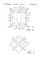
- FIG. 1is a top view of an electronic component assembly 10 that includes a leadframe 18 , an electronic component 15 , and a package 20 .
- Leadframe 18has an outer ring 11 that serves to support a plurality of leads 12 during the manufacture of electronic component assembly 10 .
- Other support structuressuch as tie bars or dambars may also be optionally used.
- outer ring 11is a temporary structure that is intended to be removed once package 20 is formed over leadframe 18 .
- Leadframe 18can be formed using a variety of techniques known in the art. For example, a stamping process could be used to form leads 12 and outer ring 11 from a single sheet of material. Leadframe 18 could also be formed using a conventional etch technique that involves forming a masking layer over a sheet of material and chemically etching the material exposed by the masking layer, thereby forming the leadframe 18 with the desired pattern. Etching processes typically allow leads 12 to be formed with smaller dimensions, whereas a stamping process is typically less expensive. It is significant to note that leadframe 18 , formed in accordance with the preferred embodiment of the present invention, is devoid of a die flag and tie bars. This can reduce the amount of material that is needed to form leadframe 18 , and thus, reduce the cost of manufacturing electronic component assembly 10 .
- Leadframe 18can be formed so that both the size and number of leads 12 can vary. As shown in FIG. 1, leadframe 18 has twenty-eight leads 12 . However, this should not be considered a limitation of the present invention. It is possible to form an electronic component assembly that has as few as two or three leads, and the maximum number of leads is only limited by the capability of the process that is used to form leadframe 18 . Current leadframe manufacturing processes can provide leadframe 18 with as many as sixty-four, one-hundred and sixty, or even five-hundred and twelve leads. Both the length (indicated in FIG. 1 with a line 19 ) and the width (indicated in FIG.
- leads 12have a length ranging from about 1 millimeter (mm) to 50 mm, and a width ranging from about 0.1 mm to 10 mm. If leadframe 18 is in a sixteen lead configuration, the length of leads 12 is preferably about 5 mm to 10 mm and their width is about 0.5 mm to 1 mm.
- leadframe 18is made from a copper alloy, but other materials such as gold, zinc, alloys comprising iron, nickel, or the like could also be used. In addition, it may be desirable to plate portions of leadframe 18 with other conductive materials such as silver or gold to improve the ability to form an electrical connection between electronic component 15 and leads 12 .
- Electronic component 15could be one a variety of discrete devices, sensing devices, semiconductor devices, or any other component used in the electronics industry.
- electronic component 15can be a discrete component (such as a thyristor, diode, etc.), a semiconductor device (such as a transistor), an integrated circuit (such as a microprocessor, a microcontroller, imaging sensor, a memory device, etc.) or a sensing device (such as an accelerometer, a pressure sensor, a chemical sensor, etc.).
- Electronic component 15is shown in FIG. 1 with dashed lines to represent its relative location on leadframe 18 and so that the underlying leads 12 can be shown.
- electronic component 15is mounted to leadframe 18 so that all of leads 12 are in physical contact with electronic component 15 . This is so that the amount of support that leadframe 18 provides to electronic component 15 through leads 12 is maximized.
- Conventional bonding techniquesthat use solder material, adhesives, or the like can be used to attach electronic component 15 to leads 12 .
- leads 12are the only portions of leadframe 18 that are in physical contact with electronic component 15 .
- bonding wiresare used to electrically connect electronic component 15 to the desired leads 12 . Again, if electronic component 15 were to have fewer than 28 bonding pads, some of leads 12 may be unused and not be electrically coupled to electronic component 15 .
- package 20is formed on leadframe 18 using an over-molding, transfer molding, compression molding, or similar molding process.
- Package 20could also be a pre-formed body component that is mounted or bonded to leadframe 18 .
- Package 20is formed so that it encapsulates at least a portion of electronic component 15 and leads 12 .
- Outer ring 11 of leadframe 18is then removed so that at least a portion of each of leads 12 extends from package 20 and so that leads 12 are electrically isolated from each other. In other words, each of leads 12 is only electrically connected to electronic component 15 through bonding wires.
- leadframe 18that is in physical contact with electronic component 15 is also electrically coupled to electronic component 15 .
- leadframe 18(such as a die flag or tie bar) that is in physical contact with electronic component 15 and electrically isolated from electronic component 15 .
- leads 12are optionally formed so as to leave a central portion of leadframe 18 open.
- the width of this openingis indicated with a line 14 .
- Electronic component 15is shown to have a square configuration that has a width indicated with a line 16 .
- the width (line 16 ) of electronic component 15is at least ten percent wider than the width (line 14 ) of any central opening so that electronic component 15 is adequately supported during the manufacture of electronic component assembly 10 .
- electronic component 15should overlap each of leads 12 by at least 100 micrometers ( ⁇ m).
- ⁇ mmicrometers
- the leadframe of the present inventioncan be used to assemble various electronic components that are each of a different size or that have a different pin requirement. This obviates the need to form a different leadframe for differently shaped electronic components.
- FIG. 2an alternative embodiment of the present invention is provided.
- leadframe 18To allow leadframe 18 to be used to assemble an electronic component 25 that is smaller than the central opening shown in FIG. 1, it is possible to form lead extensions 13 onto leads 12 .
- a second leadframe(not shown) that has lead extensions 13 is bonded to leadframe 18 .
- Lead extensions 13are individually attached to a lead 12 to fill in the central portion of leadframe 18 .
- different materialsare connected together to provide an electrical path to electronic component 25 .
- Bonding wires(not shown) are then formed from electronic component 25 to either of leads 12 or lead extensions 13 so that the portion of leads 12 that extend from package 20 are still electrically connected to electronic component 25 .
- each of leads 12have an extension 13 as it is possible to form extensions 13 on only a subset of leads 12 or form leads 12 to have the configuration shown in FIG. 2 .
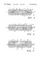
- FIG. 3is provided to illustrate how electronic component 15 (see FIG. 1) can be electrically connected to the leads 12 of leadframe 18 (see FIG. 1 ).
- electronic component 15includes bonding pads or regions 30 that are formed on the upper surface of electronic component 15 . Bonding regions represent the electrically active portions of electronic component 15 that are to be electrically connected to leads 12 . Bonding wires 31 provide electrical connection between the bonding regions 30 of electronic component 15 and leads 12 .
- one of leads 12can be used to provide a power supply voltage (e.g., Vdd) to electronic component 15
- a second lead 12can provide a power supply voltage (e.g., ground) to electronic component 15
- a third lead 12can provide a data signal to electronic component 15 (note only two leads 12 are shown in FIG. 3 ).
- each of the three leads 12could provide a different data signal to electronic component 15 .
- leads 12it may be desirable to plate at least a portion of leads 12 with silver or other material, and then form wire bonds 31 so they are connected to the portion of leads 12 that is plated with silver.
- a layer of dielectric materialsuch as silicon dioxide or silicon nitride
- an insulating materialsuch as tape can be placed along the bottom surface of electronic component 15 .
- an insulating material(not shown) can be formed on leadframe 18 or leads 12 .
- FIG. 4is provided to illustrate an alternative method of bonding electronic component 15 to leads 12 .
- the present inventioncan be used in flip-chip or tape automated bonding (TAB) assembly processes.
- TABtape automated bonding
- the tips 35 of leads 12are bent slightly so that they are the only portion of leads 12 to come into physical contact with bonding pads 30 of electronic component.
- FIG. 5is provided to illustrate how the teachings of the present invention could be used to mount a multi-chip module 43 to leads 12 .
- Multi-chip module 43comprises semiconductor devices 40 - 41 that are electrically connected to each other through bonding regions 42 . It also possible to connect semiconductor devices 40 - 41 with a leadframe positioned between the two devices, or to place semiconductor device 40 - 41 side-by-side on a single leadframe.
- the present inventioncan be used to form an electronic component assembly that is made up of multiple discrete components, integrated circuits, etc., or a combination of the possible electronic components suggested earlier with reference to FIG. 1 .
- leads 63 - 64 of a leadframeit is possible to configure the leads 63 - 64 of a leadframe so that only every other lead 63 comes in physical contact with an electronic component 61 . Even though leads 64 do not necessarily come 15 in contact with electronic component 61 , they are electrically connected to electronic component 61 by bonding wires (not shown). Thus, the only limitation on the size of the electronic component that could be formed on the leadframe is the maximum length of the bonding wire that can be formed from leads 64 to electronic component 61 . In addition, it is possible to use the same leadframe to form an electronic component assembly 60 where an electronic component 67 only comes in contact with two of leads 63 as shown with dashed lines in FIG. 6 .
- Electronic component assembly 60also includes a package 62 that is used to hold leads 63 - 64 while electronic component assembly 60 is in operation.
- FIG. 7illustrates yet another alternative embodiment for forming an electronic component assembly 70 in accordance with the present invention. It is possible to configure the leads 72 of a leadframe in a “cross” pattern to provide support to an electronic component 71 . In FIG. 7, various dashed lines are used to illustrate how the same leadframe can be used to assemble an electronic component 71 of various sizes. Again, a package 73 is used to hold and protect leads 72 and electronic component 71 while electronic component assembly 70 is in operation.
- the same leadframecan be used to form electronic component assemblies that contain electronic components of different sizes.
- the present inventionobviates the need to form a leadframe with a customized die flag for each possible electronic component that might be assembled in a high volume manufacturing operation. This not only reduces the cost associated with the die flag, but also simplifies the assembly process by allowing the same leadframe to have multiple uses.
Landscapes
- Physics & Mathematics (AREA)
- Condensed Matter Physics & Semiconductors (AREA)
- General Physics & Mathematics (AREA)
- Engineering & Computer Science (AREA)
- Computer Hardware Design (AREA)
- Microelectronics & Electronic Packaging (AREA)
- Power Engineering (AREA)
- Lead Frames For Integrated Circuits (AREA)
Abstract
Description
Claims (15)
Priority Applications (1)
| Application Number | Priority Date | Filing Date | Title |
|---|---|---|---|
| US09/106,552US6201186B1 (en) | 1998-06-29 | 1998-06-29 | Electronic component assembly and method of making the same |
Applications Claiming Priority (1)
| Application Number | Priority Date | Filing Date | Title |
|---|---|---|---|
| US09/106,552US6201186B1 (en) | 1998-06-29 | 1998-06-29 | Electronic component assembly and method of making the same |
Publications (1)
| Publication Number | Publication Date |
|---|---|
| US6201186B1true US6201186B1 (en) | 2001-03-13 |
Family
ID=22312034
Family Applications (1)
| Application Number | Title | Priority Date | Filing Date |
|---|---|---|---|
| US09/106,552Expired - LifetimeUS6201186B1 (en) | 1998-06-29 | 1998-06-29 | Electronic component assembly and method of making the same |
Country Status (1)
| Country | Link |
|---|---|
| US (1) | US6201186B1 (en) |
Cited By (117)
| Publication number | Priority date | Publication date | Assignee | Title |
|---|---|---|---|---|
| US6577508B1 (en)* | 2000-08-10 | 2003-06-10 | Nortel Networks Limited | Multilayer circuit board |
| US6597059B1 (en)* | 2001-04-04 | 2003-07-22 | Amkor Technology, Inc. | Thermally enhanced chip scale lead on chip semiconductor package |
| EP1336993A1 (en)* | 2002-02-18 | 2003-08-20 | STMicroelectronics S.r.l. | Assembly structure for electronic power integrated circuit formed on a semiconductor die and corresponding manufacturing process |
| US6627976B1 (en)* | 1999-10-15 | 2003-09-30 | Amkor Technology, Inc. | Leadframe for semiconductor package and mold for molding the same |
| US20030197290A1 (en)* | 1999-12-16 | 2003-10-23 | Crowley Sean Timothy | Stackable semiconductor package and method for manufacturing same |
| US20040065905A1 (en)* | 2001-03-27 | 2004-04-08 | Jong Sik Paek | Semiconductor package and method for manufacturing the same |
| US6750545B1 (en) | 2003-02-28 | 2004-06-15 | Amkor Technology, Inc. | Semiconductor package capable of die stacking |
| US20040150086A1 (en)* | 1999-10-15 | 2004-08-05 | Lee Tae Heon | Semiconductor package having reduced thickness |
| US6777789B1 (en) | 2001-03-20 | 2004-08-17 | Amkor Technology, Inc. | Mounting for a package containing a chip |
| US6794740B1 (en) | 2003-03-13 | 2004-09-21 | Amkor Technology, Inc. | Leadframe package for semiconductor devices |
| US6798047B1 (en) | 2002-12-26 | 2004-09-28 | Amkor Technology, Inc. | Pre-molded leadframe |
| US6818973B1 (en) | 2002-09-09 | 2004-11-16 | Amkor Technology, Inc. | Exposed lead QFP package fabricated through the use of a partial saw process |
| US6873041B1 (en) | 2001-11-07 | 2005-03-29 | Amkor Technology, Inc. | Power semiconductor package with strap |
| US6879034B1 (en) | 2003-05-01 | 2005-04-12 | Amkor Technology, Inc. | Semiconductor package including low temperature co-fired ceramic substrate |
| US6893900B1 (en) | 1998-06-24 | 2005-05-17 | Amkor Technology, Inc. | Method of making an integrated circuit package |
| US6897550B1 (en) | 2003-06-11 | 2005-05-24 | Amkor Technology, Inc. | Fully-molded leadframe stand-off feature |
| US6919620B1 (en) | 2002-09-17 | 2005-07-19 | Amkor Technology, Inc. | Compact flash memory card with clamshell leadframe |
| US6921967B2 (en) | 2003-09-24 | 2005-07-26 | Amkor Technology, Inc. | Reinforced die pad support structure |
| US20050212496A1 (en)* | 2004-03-26 | 2005-09-29 | Marvell World Trade Ltd. | Voltage regulator |
| US6953988B2 (en) | 2000-03-25 | 2005-10-11 | Amkor Technology, Inc. | Semiconductor package |
| US6965157B1 (en) | 1999-11-09 | 2005-11-15 | Amkor Technology, Inc. | Semiconductor package with exposed die pad and body-locking leadframe |
| US6965159B1 (en) | 2001-09-19 | 2005-11-15 | Amkor Technology, Inc. | Reinforced lead-frame assembly for interconnecting circuits within a circuit module |
| US6967395B1 (en) | 2001-03-20 | 2005-11-22 | Amkor Technology, Inc. | Mounting for a package containing a chip |
| US7001799B1 (en) | 2003-03-13 | 2006-02-21 | Amkor Technology, Inc. | Method of making a leadframe for semiconductor devices |
| US7005326B1 (en) | 1998-06-24 | 2006-02-28 | Amkor Technology, Inc. | Method of making an integrated circuit package |
| US7008825B1 (en) | 2003-05-27 | 2006-03-07 | Amkor Technology, Inc. | Leadframe strip having enhanced testability |
| US7030474B1 (en) | 1998-06-24 | 2006-04-18 | Amkor Technology, Inc. | Plastic integrated circuit package and method and leadframe for making the package |
| US20060082430A1 (en)* | 2003-07-16 | 2006-04-20 | Marvell International Ltd. | Power inductor with reduced DC current saturation |
| US7045882B2 (en) | 2000-12-29 | 2006-05-16 | Amkor Technology, Inc. | Semiconductor package including flip chip |
| US7045883B1 (en) | 2001-04-04 | 2006-05-16 | Amkor Technology, Inc. | Thermally enhanced chip scale lead on chip semiconductor package and method of making same |
| US20060114091A1 (en)* | 2003-07-16 | 2006-06-01 | Marvell World Trade, Ltd. | Power inductor with reduced DC current saturation |
| US7057280B2 (en) | 1998-11-20 | 2006-06-06 | Amkor Technology, Inc. | Leadframe having lead locks to secure leads to encapsulant |
| US7057268B1 (en) | 2004-01-27 | 2006-06-06 | Amkor Technology, Inc. | Cavity case with clip/plug for use on multi-media card |
| US7064009B1 (en) | 2001-04-04 | 2006-06-20 | Amkor Technology, Inc. | Thermally enhanced chip scale lead on chip semiconductor package and method of making same |
| US7071541B1 (en) | 1998-06-24 | 2006-07-04 | Amkor Technology, Inc. | Plastic integrated circuit package and method and leadframe for making the package |
| US20060158297A1 (en)* | 2003-07-16 | 2006-07-20 | Marvell World Trade Ltd. | Power inductor with reduced DC current saturation |
| US7091594B1 (en) | 2004-01-28 | 2006-08-15 | Amkor Technology, Inc. | Leadframe type semiconductor package having reduced inductance and its manufacturing method |
| US7095103B1 (en) | 2003-05-01 | 2006-08-22 | Amkor Technology, Inc. | Leadframe based memory card |
| US7102208B1 (en) | 1999-10-15 | 2006-09-05 | Amkor Technology, Inc. | Leadframe and semiconductor package with improved solder joint strength |
| US7112474B1 (en) | 1998-06-24 | 2006-09-26 | Amkor Technology, Inc. | Method of making an integrated circuit package |
| US20060244130A1 (en)* | 2005-04-29 | 2006-11-02 | Holtek Semiconductor Inc. | Multi-chip semiconductor package |
| US7138707B1 (en) | 2003-10-21 | 2006-11-21 | Amkor Technology, Inc. | Semiconductor package including leads and conductive posts for providing increased functionality |
| US7144517B1 (en) | 2003-11-07 | 2006-12-05 | Amkor Technology, Inc. | Manufacturing method for leadframe and for semiconductor package using the leadframe |
| US7170150B2 (en) | 2001-03-27 | 2007-01-30 | Amkor Technology, Inc. | Lead frame for semiconductor package |
| US7183630B1 (en) | 2002-04-15 | 2007-02-27 | Amkor Technology, Inc. | Lead frame with plated end leads |
| US7190062B1 (en) | 2004-06-15 | 2007-03-13 | Amkor Technology, Inc. | Embedded leadframe semiconductor package |
| US7192807B1 (en) | 2002-11-08 | 2007-03-20 | Amkor Technology, Inc. | Wafer level package and fabrication method |
| US7202554B1 (en) | 2004-08-19 | 2007-04-10 | Amkor Technology, Inc. | Semiconductor package and its manufacturing method |
| US7211879B1 (en) | 2003-11-12 | 2007-05-01 | Amkor Technology, Inc. | Semiconductor package with chamfered corners and method of manufacturing the same |
| US7217991B1 (en) | 2004-10-22 | 2007-05-15 | Amkor Technology, Inc. | Fan-in leadframe semiconductor package |
| US7245007B1 (en) | 2003-09-18 | 2007-07-17 | Amkor Technology, Inc. | Exposed lead interposer leadframe package |
| US7253503B1 (en) | 1999-11-05 | 2007-08-07 | Amkor Technology, Inc. | Integrated circuit device packages and substrates for making the packages |
| US7332375B1 (en) | 1998-06-24 | 2008-02-19 | Amkor Technology, Inc. | Method of making an integrated circuit package |
| US7361533B1 (en) | 2002-11-08 | 2008-04-22 | Amkor Technology, Inc. | Stacked embedded leadframe |
| US7485952B1 (en) | 2001-09-19 | 2009-02-03 | Amkor Technology, Inc. | Drop resistant bumpers for fully molded memory cards |
| US7507603B1 (en) | 2005-12-02 | 2009-03-24 | Amkor Technology, Inc. | Etch singulated semiconductor package |
| US7535085B2 (en) | 1999-10-15 | 2009-05-19 | Amkor Technology, Inc. | Semiconductor package having improved adhesiveness and ground bonding |
| US7572681B1 (en) | 2005-12-08 | 2009-08-11 | Amkor Technology, Inc. | Embedded electronic component package |
| US7598598B1 (en) | 2003-02-05 | 2009-10-06 | Amkor Technology, Inc. | Offset etched corner leads for semiconductor package |
| US7687899B1 (en) | 2007-08-07 | 2010-03-30 | Amkor Technology, Inc. | Dual laminate package structure with embedded elements |
| US7687893B2 (en) | 2006-12-27 | 2010-03-30 | Amkor Technology, Inc. | Semiconductor package having leadframe with exposed anchor pads |
| US7723210B2 (en) | 2002-11-08 | 2010-05-25 | Amkor Technology, Inc. | Direct-write wafer level chip scale package |
| US7723852B1 (en) | 2008-01-21 | 2010-05-25 | Amkor Technology, Inc. | Stacked semiconductor package and method of making same |
| US7768135B1 (en) | 2008-04-17 | 2010-08-03 | Amkor Technology, Inc. | Semiconductor package with fast power-up cycle and method of making same |
| US7777351B1 (en) | 2007-10-01 | 2010-08-17 | Amkor Technology, Inc. | Thin stacked interposer package |
| US7808084B1 (en) | 2008-05-06 | 2010-10-05 | Amkor Technology, Inc. | Semiconductor package with half-etched locking features |
| US7829990B1 (en) | 2007-01-18 | 2010-11-09 | Amkor Technology, Inc. | Stackable semiconductor package including laminate interposer |
| US7847386B1 (en) | 2007-11-05 | 2010-12-07 | Amkor Technology, Inc. | Reduced size stacked semiconductor package and method of making the same |
| US7847392B1 (en) | 2008-09-30 | 2010-12-07 | Amkor Technology, Inc. | Semiconductor device including leadframe with increased I/O |
| US7875963B1 (en) | 2008-11-21 | 2011-01-25 | Amkor Technology, Inc. | Semiconductor device including leadframe having power bars and increased I/O |
| US7902660B1 (en) | 2006-05-24 | 2011-03-08 | Amkor Technology, Inc. | Substrate for semiconductor device and manufacturing method thereof |
| US7956453B1 (en) | 2008-01-16 | 2011-06-07 | Amkor Technology, Inc. | Semiconductor package with patterning layer and method of making same |
| US7960818B1 (en) | 2009-03-04 | 2011-06-14 | Amkor Technology, Inc. | Conformal shield on punch QFN semiconductor package |
| US7968998B1 (en) | 2006-06-21 | 2011-06-28 | Amkor Technology, Inc. | Side leaded, bottom exposed pad and bottom exposed lead fusion quad flat semiconductor package |
| US7977774B2 (en) | 2007-07-10 | 2011-07-12 | Amkor Technology, Inc. | Fusion quad flat semiconductor package |
| US7982297B1 (en) | 2007-03-06 | 2011-07-19 | Amkor Technology, Inc. | Stackable semiconductor package having partially exposed semiconductor die and method of fabricating the same |
| US7982298B1 (en) | 2008-12-03 | 2011-07-19 | Amkor Technology, Inc. | Package in package semiconductor device |
| US7989933B1 (en) | 2008-10-06 | 2011-08-02 | Amkor Technology, Inc. | Increased I/O leadframe and semiconductor device including same |
| US8008758B1 (en) | 2008-10-27 | 2011-08-30 | Amkor Technology, Inc. | Semiconductor device with increased I/O leadframe |
| US8026589B1 (en) | 2009-02-23 | 2011-09-27 | Amkor Technology, Inc. | Reduced profile stackable semiconductor package |
| US8058715B1 (en) | 2009-01-09 | 2011-11-15 | Amkor Technology, Inc. | Package in package device for RF transceiver module |
| US8067821B1 (en) | 2008-04-10 | 2011-11-29 | Amkor Technology, Inc. | Flat semiconductor package with half package molding |
| US8072050B1 (en) | 2008-11-18 | 2011-12-06 | Amkor Technology, Inc. | Semiconductor device with increased I/O leadframe including passive device |
| US8089159B1 (en) | 2007-10-03 | 2012-01-03 | Amkor Technology, Inc. | Semiconductor package with increased I/O density and method of making the same |
| US8089145B1 (en) | 2008-11-17 | 2012-01-03 | Amkor Technology, Inc. | Semiconductor device including increased capacity leadframe |
| US8125064B1 (en) | 2008-07-28 | 2012-02-28 | Amkor Technology, Inc. | Increased I/O semiconductor package and method of making same |
| US8184453B1 (en) | 2008-07-31 | 2012-05-22 | Amkor Technology, Inc. | Increased capacity semiconductor package |
| US8294276B1 (en) | 2010-05-27 | 2012-10-23 | Amkor Technology, Inc. | Semiconductor device and fabricating method thereof |
| US8318287B1 (en) | 1998-06-24 | 2012-11-27 | Amkor Technology, Inc. | Integrated circuit package and method of making the same |
| US8324511B1 (en) | 2010-04-06 | 2012-12-04 | Amkor Technology, Inc. | Through via nub reveal method and structure |
| US8390130B1 (en) | 2011-01-06 | 2013-03-05 | Amkor Technology, Inc. | Through via recessed reveal structure and method |
| US8410585B2 (en) | 2000-04-27 | 2013-04-02 | Amkor Technology, Inc. | Leadframe and semiconductor package made using the leadframe |
| US8440554B1 (en) | 2010-08-02 | 2013-05-14 | Amkor Technology, Inc. | Through via connected backside embedded circuit features structure and method |
| US8487420B1 (en) | 2008-12-08 | 2013-07-16 | Amkor Technology, Inc. | Package in package semiconductor device with film over wire |
| US8487445B1 (en) | 2010-10-05 | 2013-07-16 | Amkor Technology, Inc. | Semiconductor device having through electrodes protruding from dielectric layer |
| US8552548B1 (en) | 2011-11-29 | 2013-10-08 | Amkor Technology, Inc. | Conductive pad on protruding through electrode semiconductor device |
| US8575742B1 (en) | 2009-04-06 | 2013-11-05 | Amkor Technology, Inc. | Semiconductor device with increased I/O leadframe including power bars |
| US8648450B1 (en) | 2011-01-27 | 2014-02-11 | Amkor Technology, Inc. | Semiconductor device including leadframe with a combination of leads and lands |
| US8674485B1 (en) | 2010-12-08 | 2014-03-18 | Amkor Technology, Inc. | Semiconductor device including leadframe with downsets |
| US8680656B1 (en) | 2009-01-05 | 2014-03-25 | Amkor Technology, Inc. | Leadframe structure for concentrated photovoltaic receiver package |
| US8791501B1 (en) | 2010-12-03 | 2014-07-29 | Amkor Technology, Inc. | Integrated passive device structure and method |
| US8796561B1 (en) | 2009-10-05 | 2014-08-05 | Amkor Technology, Inc. | Fan out build up substrate stackable package and method |
| US20140252581A1 (en)* | 2013-03-05 | 2014-09-11 | Mariano Layson Ching, Jr. | Lead frame and substrate semiconductor package |
| US8937381B1 (en) | 2009-12-03 | 2015-01-20 | Amkor Technology, Inc. | Thin stackable package and method |
| US8957510B2 (en) | 2013-07-03 | 2015-02-17 | Freescale Semiconductor, Inc. | Using an integrated circuit die configuration for package height reduction |
| US9048298B1 (en) | 2012-03-29 | 2015-06-02 | Amkor Technology, Inc. | Backside warpage control structure and fabrication method |
| US9129943B1 (en) | 2012-03-29 | 2015-09-08 | Amkor Technology, Inc. | Embedded component package and fabrication method |
| US9184118B2 (en) | 2013-05-02 | 2015-11-10 | Amkor Technology Inc. | Micro lead frame structure having reinforcing portions and method |
| US9184148B2 (en) | 2013-10-24 | 2015-11-10 | Amkor Technology, Inc. | Semiconductor package and method therefor |
| US9631481B1 (en) | 2011-01-27 | 2017-04-25 | Amkor Technology, Inc. | Semiconductor device including leadframe with a combination of leads and lands and method |
| US9673122B2 (en) | 2014-05-02 | 2017-06-06 | Amkor Technology, Inc. | Micro lead frame structure having reinforcing portions and method |
| US9679834B2 (en)* | 2007-07-24 | 2017-06-13 | Micron Technology, Inc. | Semiconductor dies with recesses, associated leadframes, and associated systems and methods |
| US9691734B1 (en) | 2009-12-07 | 2017-06-27 | Amkor Technology, Inc. | Method of forming a plurality of electronic component packages |
| US9704725B1 (en) | 2012-03-06 | 2017-07-11 | Amkor Technology, Inc. | Semiconductor device with leadframe configured to facilitate reduced burr formation |
| US10811341B2 (en) | 2009-01-05 | 2020-10-20 | Amkor Technology Singapore Holding Pte Ltd. | Semiconductor device with through-mold via |
| US20230088833A1 (en)* | 2021-09-21 | 2023-03-23 | Infineon Technologies Austria Ag | Semiconductor package and lead frame with enhanced device isolation |
| DE102023129401A1 (en) | 2023-10-25 | 2025-04-30 | Infineon Technologies Ag | Package carrier with large corner terminals and terminal tip inspection feature |
Citations (17)
| Publication number | Priority date | Publication date | Assignee | Title |
|---|---|---|---|---|
| US3716761A (en) | 1972-05-03 | 1973-02-13 | Microsystems Int Ltd | Universal interconnection structure for microelectronic devices |
| US3902148A (en) | 1970-11-27 | 1975-08-26 | Signetics Corp | Semiconductor lead structure and assembly and method for fabricating same |
| US4466183A (en) | 1982-05-03 | 1984-08-21 | National Semiconductor Corporation | Integrated circuit packaging process |
| US4489365A (en) | 1982-09-17 | 1984-12-18 | Burroughs Corporation | Universal leadless chip carrier mounting pad |
| US4578697A (en) | 1981-06-15 | 1986-03-25 | Fujitsu Limited | Semiconductor device encapsulating a multi-chip array |
| US4595945A (en) | 1983-10-21 | 1986-06-17 | At&T Bell Laboratories | Plastic package with lead frame crossunder |
| US4612564A (en) | 1984-06-04 | 1986-09-16 | At&T Bell Laboratories | Plastic integrated circuit package |
| US4680613A (en) | 1983-12-01 | 1987-07-14 | Fairchild Semiconductor Corporation | Low impedance package for integrated circuit die |
| US4711700A (en)* | 1985-07-03 | 1987-12-08 | United Technologies Corporation | Method for densifying leadframe conductor spacing |
| US4870356A (en) | 1987-09-30 | 1989-09-26 | Digital Equipment Corporation | Multi-component test fixture |
| US4924291A (en) | 1988-10-24 | 1990-05-08 | Motorola Inc. | Flagless semiconductor package |
| US5245214A (en)* | 1991-06-06 | 1993-09-14 | Northern Telecom Limited | Method of designing a leadframe and a leadframe created thereby |
| US5378656A (en) | 1992-03-27 | 1995-01-03 | Hitachi, Ltd. | Leadframe, semiconductor integrated circuit device using the same, and method of and process for fabricating the same |
| US5437915A (en)* | 1992-01-17 | 1995-08-01 | Hitachi, Ltd. | Semiconductor leadframe and its production method and plastic encapsulated semiconductor device |
| US5596225A (en)* | 1994-10-27 | 1997-01-21 | National Semiconductor Corporation | Leadframe for an integrated circuit package which electrically interconnects multiple integrated circuit die |
| US5796159A (en) | 1995-11-30 | 1998-08-18 | Analog Devices, Inc. | Thermally efficient integrated circuit package |
| US5939781A (en)* | 1996-09-26 | 1999-08-17 | Texas Instruments Incorporated | Thermally enhanced integrated circuit packaging system |
- 1998
- 1998-06-29USUS09/106,552patent/US6201186B1/ennot_activeExpired - Lifetime
Patent Citations (17)
| Publication number | Priority date | Publication date | Assignee | Title |
|---|---|---|---|---|
| US3902148A (en) | 1970-11-27 | 1975-08-26 | Signetics Corp | Semiconductor lead structure and assembly and method for fabricating same |
| US3716761A (en) | 1972-05-03 | 1973-02-13 | Microsystems Int Ltd | Universal interconnection structure for microelectronic devices |
| US4578697A (en) | 1981-06-15 | 1986-03-25 | Fujitsu Limited | Semiconductor device encapsulating a multi-chip array |
| US4466183A (en) | 1982-05-03 | 1984-08-21 | National Semiconductor Corporation | Integrated circuit packaging process |
| US4489365A (en) | 1982-09-17 | 1984-12-18 | Burroughs Corporation | Universal leadless chip carrier mounting pad |
| US4595945A (en) | 1983-10-21 | 1986-06-17 | At&T Bell Laboratories | Plastic package with lead frame crossunder |
| US4680613A (en) | 1983-12-01 | 1987-07-14 | Fairchild Semiconductor Corporation | Low impedance package for integrated circuit die |
| US4612564A (en) | 1984-06-04 | 1986-09-16 | At&T Bell Laboratories | Plastic integrated circuit package |
| US4711700A (en)* | 1985-07-03 | 1987-12-08 | United Technologies Corporation | Method for densifying leadframe conductor spacing |
| US4870356A (en) | 1987-09-30 | 1989-09-26 | Digital Equipment Corporation | Multi-component test fixture |
| US4924291A (en) | 1988-10-24 | 1990-05-08 | Motorola Inc. | Flagless semiconductor package |
| US5245214A (en)* | 1991-06-06 | 1993-09-14 | Northern Telecom Limited | Method of designing a leadframe and a leadframe created thereby |
| US5437915A (en)* | 1992-01-17 | 1995-08-01 | Hitachi, Ltd. | Semiconductor leadframe and its production method and plastic encapsulated semiconductor device |
| US5378656A (en) | 1992-03-27 | 1995-01-03 | Hitachi, Ltd. | Leadframe, semiconductor integrated circuit device using the same, and method of and process for fabricating the same |
| US5596225A (en)* | 1994-10-27 | 1997-01-21 | National Semiconductor Corporation | Leadframe for an integrated circuit package which electrically interconnects multiple integrated circuit die |
| US5796159A (en) | 1995-11-30 | 1998-08-18 | Analog Devices, Inc. | Thermally efficient integrated circuit package |
| US5939781A (en)* | 1996-09-26 | 1999-08-17 | Texas Instruments Incorporated | Thermally enhanced integrated circuit packaging system |
Cited By (201)
| Publication number | Priority date | Publication date | Assignee | Title |
|---|---|---|---|---|
| US6893900B1 (en) | 1998-06-24 | 2005-05-17 | Amkor Technology, Inc. | Method of making an integrated circuit package |
| US8318287B1 (en) | 1998-06-24 | 2012-11-27 | Amkor Technology, Inc. | Integrated circuit package and method of making the same |
| US7005326B1 (en) | 1998-06-24 | 2006-02-28 | Amkor Technology, Inc. | Method of making an integrated circuit package |
| US7071541B1 (en) | 1998-06-24 | 2006-07-04 | Amkor Technology, Inc. | Plastic integrated circuit package and method and leadframe for making the package |
| US8853836B1 (en) | 1998-06-24 | 2014-10-07 | Amkor Technology, Inc. | Integrated circuit package and method of making the same |
| US8963301B1 (en) | 1998-06-24 | 2015-02-24 | Amkor Technology, Inc. | Integrated circuit package and method of making the same |
| US7030474B1 (en) | 1998-06-24 | 2006-04-18 | Amkor Technology, Inc. | Plastic integrated circuit package and method and leadframe for making the package |
| US7112474B1 (en) | 1998-06-24 | 2006-09-26 | Amkor Technology, Inc. | Method of making an integrated circuit package |
| US7560804B1 (en) | 1998-06-24 | 2009-07-14 | Amkor Technology, Inc. | Integrated circuit package and method of making the same |
| US9224676B1 (en) | 1998-06-24 | 2015-12-29 | Amkor Technology, Inc. | Integrated circuit package and method of making the same |
| US7332375B1 (en) | 1998-06-24 | 2008-02-19 | Amkor Technology, Inc. | Method of making an integrated circuit package |
| US7057280B2 (en) | 1998-11-20 | 2006-06-06 | Amkor Technology, Inc. | Leadframe having lead locks to secure leads to encapsulant |
| US7564122B2 (en) | 1998-11-20 | 2009-07-21 | Amkor Technology, Inc. | Semiconductor package and method of making using leadframe having lead locks to secure leads to encapsulant |
| US7102208B1 (en) | 1999-10-15 | 2006-09-05 | Amkor Technology, Inc. | Leadframe and semiconductor package with improved solder joint strength |
| US7115445B2 (en) | 1999-10-15 | 2006-10-03 | Amkor Technology, Inc. | Semiconductor package having reduced thickness |
| US6627976B1 (en)* | 1999-10-15 | 2003-09-30 | Amkor Technology, Inc. | Leadframe for semiconductor package and mold for molding the same |
| US7321162B1 (en) | 1999-10-15 | 2008-01-22 | Amkor Technology, Inc. | Semiconductor package having reduced thickness |
| US20040150086A1 (en)* | 1999-10-15 | 2004-08-05 | Lee Tae Heon | Semiconductor package having reduced thickness |
| US7535085B2 (en) | 1999-10-15 | 2009-05-19 | Amkor Technology, Inc. | Semiconductor package having improved adhesiveness and ground bonding |
| US7253503B1 (en) | 1999-11-05 | 2007-08-07 | Amkor Technology, Inc. | Integrated circuit device packages and substrates for making the packages |
| US6965157B1 (en) | 1999-11-09 | 2005-11-15 | Amkor Technology, Inc. | Semiconductor package with exposed die pad and body-locking leadframe |
| US20030197290A1 (en)* | 1999-12-16 | 2003-10-23 | Crowley Sean Timothy | Stackable semiconductor package and method for manufacturing same |
| US7045396B2 (en) | 1999-12-16 | 2006-05-16 | Amkor Technology, Inc. | Stackable semiconductor package and method for manufacturing same |
| US6953988B2 (en) | 2000-03-25 | 2005-10-11 | Amkor Technology, Inc. | Semiconductor package |
| US9362210B2 (en) | 2000-04-27 | 2016-06-07 | Amkor Technology, Inc. | Leadframe and semiconductor package made using the leadframe |
| US8410585B2 (en) | 2000-04-27 | 2013-04-02 | Amkor Technology, Inc. | Leadframe and semiconductor package made using the leadframe |
| US6577508B1 (en)* | 2000-08-10 | 2003-06-10 | Nortel Networks Limited | Multilayer circuit board |
| US7051433B1 (en) | 2000-08-10 | 2006-05-30 | Nortel Networks Limited | Multilayer circuit board |
| US7045882B2 (en) | 2000-12-29 | 2006-05-16 | Amkor Technology, Inc. | Semiconductor package including flip chip |
| US6777789B1 (en) | 2001-03-20 | 2004-08-17 | Amkor Technology, Inc. | Mounting for a package containing a chip |
| US6967395B1 (en) | 2001-03-20 | 2005-11-22 | Amkor Technology, Inc. | Mounting for a package containing a chip |
| US7928542B2 (en) | 2001-03-27 | 2011-04-19 | Amkor Technology, Inc. | Lead frame for semiconductor package |
| US8102037B2 (en) | 2001-03-27 | 2012-01-24 | Amkor Technology, Inc. | Leadframe for semiconductor package |
| US7521294B2 (en) | 2001-03-27 | 2009-04-21 | Amkor Technology, Inc. | Lead frame for semiconductor package |
| US20040065905A1 (en)* | 2001-03-27 | 2004-04-08 | Jong Sik Paek | Semiconductor package and method for manufacturing the same |
| US20090166842A1 (en)* | 2001-03-27 | 2009-07-02 | Hyung Ju Lee | Leadframe for semiconductor package |
| US6846704B2 (en) | 2001-03-27 | 2005-01-25 | Amkor Technology, Inc. | Semiconductor package and method for manufacturing the same |
| US7170150B2 (en) | 2001-03-27 | 2007-01-30 | Amkor Technology, Inc. | Lead frame for semiconductor package |
| US6597059B1 (en)* | 2001-04-04 | 2003-07-22 | Amkor Technology, Inc. | Thermally enhanced chip scale lead on chip semiconductor package |
| US7064009B1 (en) | 2001-04-04 | 2006-06-20 | Amkor Technology, Inc. | Thermally enhanced chip scale lead on chip semiconductor package and method of making same |
| US7045883B1 (en) | 2001-04-04 | 2006-05-16 | Amkor Technology, Inc. | Thermally enhanced chip scale lead on chip semiconductor package and method of making same |
| US6873032B1 (en) | 2001-04-04 | 2005-03-29 | Amkor Technology, Inc. | Thermally enhanced chip scale lead on chip semiconductor package and method of making same |
| US6965159B1 (en) | 2001-09-19 | 2005-11-15 | Amkor Technology, Inc. | Reinforced lead-frame assembly for interconnecting circuits within a circuit module |
| US6998702B1 (en) | 2001-09-19 | 2006-02-14 | Amkor Technology, Inc. | Front edge chamfer feature for fully-molded memory cards |
| US7485952B1 (en) | 2001-09-19 | 2009-02-03 | Amkor Technology, Inc. | Drop resistant bumpers for fully molded memory cards |
| US6873041B1 (en) | 2001-11-07 | 2005-03-29 | Amkor Technology, Inc. | Power semiconductor package with strap |
| EP1336993A1 (en)* | 2002-02-18 | 2003-08-20 | STMicroelectronics S.r.l. | Assembly structure for electronic power integrated circuit formed on a semiconductor die and corresponding manufacturing process |
| US20030209783A1 (en)* | 2002-02-18 | 2003-11-13 | Stmicroelectronics S.R.I. | Assembly structure for electronic power integrated circuit formed on a semiconductor die and corresponding manufacturing process |
| US7459771B2 (en) | 2002-02-18 | 2008-12-02 | Stmicroelectronics, S.R.L. | Assembly structure for electronic power integrated circuit formed on a semiconductor die and corresponding manufacturing process |
| US7183630B1 (en) | 2002-04-15 | 2007-02-27 | Amkor Technology, Inc. | Lead frame with plated end leads |
| US7211471B1 (en) | 2002-09-09 | 2007-05-01 | Amkor Technology, Inc. | Exposed lead QFP package fabricated through the use of a partial saw process |
| US6995459B2 (en) | 2002-09-09 | 2006-02-07 | Amkor Technology, Inc. | Semiconductor package with increased number of input and output pins |
| US6818973B1 (en) | 2002-09-09 | 2004-11-16 | Amkor Technology, Inc. | Exposed lead QFP package fabricated through the use of a partial saw process |
| US6876068B1 (en) | 2002-09-09 | 2005-04-05 | Amkor Technology, Inc | Semiconductor package with increased number of input and output pins |
| US6919620B1 (en) | 2002-09-17 | 2005-07-19 | Amkor Technology, Inc. | Compact flash memory card with clamshell leadframe |
| US7714431B1 (en) | 2002-11-08 | 2010-05-11 | Amkor Technology, Inc. | Electronic component package comprising fan-out and fan-in traces |
| US8710649B1 (en) | 2002-11-08 | 2014-04-29 | Amkor Technology, Inc. | Wafer level package and fabrication method |
| US7192807B1 (en) | 2002-11-08 | 2007-03-20 | Amkor Technology, Inc. | Wafer level package and fabrication method |
| US8501543B1 (en) | 2002-11-08 | 2013-08-06 | Amkor Technology, Inc. | Direct-write wafer level chip scale package |
| US8691632B1 (en) | 2002-11-08 | 2014-04-08 | Amkor Technology, Inc. | Wafer level package and fabrication method |
| US9406645B1 (en) | 2002-11-08 | 2016-08-02 | Amkor Technology, Inc. | Wafer level package and fabrication method |
| US8119455B1 (en) | 2002-11-08 | 2012-02-21 | Amkor Technology, Inc. | Wafer level package fabrication method |
| US10665567B1 (en) | 2002-11-08 | 2020-05-26 | Amkor Technology, Inc. | Wafer level package and fabrication method |
| US7247523B1 (en) | 2002-11-08 | 2007-07-24 | Amkor Technology, Inc. | Two-sided wafer escape package |
| US7692286B1 (en) | 2002-11-08 | 2010-04-06 | Amkor Technology, Inc. | Two-sided fan-out wafer escape package |
| US7723210B2 (en) | 2002-11-08 | 2010-05-25 | Amkor Technology, Inc. | Direct-write wafer level chip scale package |
| US8188584B1 (en) | 2002-11-08 | 2012-05-29 | Amkor Technology, Inc. | Direct-write wafer level chip scale package |
| US7361533B1 (en) | 2002-11-08 | 2008-04-22 | Amkor Technology, Inc. | Stacked embedded leadframe |
| US7420272B1 (en) | 2002-11-08 | 2008-09-02 | Amkor Technology, Inc. | Two-sided wafer escape package |
| US8486764B1 (en) | 2002-11-08 | 2013-07-16 | Amkor Technology, Inc. | Wafer level package and fabrication method |
| US8298866B1 (en) | 2002-11-08 | 2012-10-30 | Amkor Technology, Inc. | Wafer level package and fabrication method |
| US9871015B1 (en) | 2002-11-08 | 2018-01-16 | Amkor Technology, Inc. | Wafer level package and fabrication method |
| US8952522B1 (en) | 2002-11-08 | 2015-02-10 | Amkor Technology, Inc. | Wafer level package and fabrication method |
| US9054117B1 (en) | 2002-11-08 | 2015-06-09 | Amkor Technology, Inc. | Wafer level package and fabrication method |
| US7932595B1 (en) | 2002-11-08 | 2011-04-26 | Amkor Technology, Inc. | Electronic component package comprising fan-out traces |
| US6798047B1 (en) | 2002-12-26 | 2004-09-28 | Amkor Technology, Inc. | Pre-molded leadframe |
| US7598598B1 (en) | 2003-02-05 | 2009-10-06 | Amkor Technology, Inc. | Offset etched corner leads for semiconductor package |
| US6750545B1 (en) | 2003-02-28 | 2004-06-15 | Amkor Technology, Inc. | Semiconductor package capable of die stacking |
| US6794740B1 (en) | 2003-03-13 | 2004-09-21 | Amkor Technology, Inc. | Leadframe package for semiconductor devices |
| US7001799B1 (en) | 2003-03-13 | 2006-02-21 | Amkor Technology, Inc. | Method of making a leadframe for semiconductor devices |
| US7095103B1 (en) | 2003-05-01 | 2006-08-22 | Amkor Technology, Inc. | Leadframe based memory card |
| US6879034B1 (en) | 2003-05-01 | 2005-04-12 | Amkor Technology, Inc. | Semiconductor package including low temperature co-fired ceramic substrate |
| US7008825B1 (en) | 2003-05-27 | 2006-03-07 | Amkor Technology, Inc. | Leadframe strip having enhanced testability |
| US6897550B1 (en) | 2003-06-11 | 2005-05-24 | Amkor Technology, Inc. | Fully-molded leadframe stand-off feature |
| US8028401B2 (en) | 2003-07-16 | 2011-10-04 | Marvell World Trade Ltd. | Method of fabricating a conducting crossover structure for a power inductor |
| US20060158297A1 (en)* | 2003-07-16 | 2006-07-20 | Marvell World Trade Ltd. | Power inductor with reduced DC current saturation |
| US7987580B2 (en)* | 2003-07-16 | 2011-08-02 | Marvell World Trade Ltd. | Method of fabricating conductor crossover structure for power inductor |
| US20060082430A1 (en)* | 2003-07-16 | 2006-04-20 | Marvell International Ltd. | Power inductor with reduced DC current saturation |
| US8098123B2 (en) | 2003-07-16 | 2012-01-17 | Marvell World Trade Ltd. | Power inductor with reduced DC current saturation |
| US20070163110A1 (en)* | 2003-07-16 | 2007-07-19 | Marvell World Trade Ltd. | Power inductor with reduced DC current saturation |
| US20060114091A1 (en)* | 2003-07-16 | 2006-06-01 | Marvell World Trade, Ltd. | Power inductor with reduced DC current saturation |
| US8035471B2 (en) | 2003-07-16 | 2011-10-11 | Marvell World Trade Ltd. | Power inductor with reduced DC current saturation |
| US7245007B1 (en) | 2003-09-18 | 2007-07-17 | Amkor Technology, Inc. | Exposed lead interposer leadframe package |
| US6921967B2 (en) | 2003-09-24 | 2005-07-26 | Amkor Technology, Inc. | Reinforced die pad support structure |
| US7138707B1 (en) | 2003-10-21 | 2006-11-21 | Amkor Technology, Inc. | Semiconductor package including leads and conductive posts for providing increased functionality |
| US7214326B1 (en) | 2003-11-07 | 2007-05-08 | Amkor Technology, Inc. | Increased capacity leadframe and semiconductor package using the same |
| US7144517B1 (en) | 2003-11-07 | 2006-12-05 | Amkor Technology, Inc. | Manufacturing method for leadframe and for semiconductor package using the leadframe |
| US7211879B1 (en) | 2003-11-12 | 2007-05-01 | Amkor Technology, Inc. | Semiconductor package with chamfered corners and method of manufacturing the same |
| US7057268B1 (en) | 2004-01-27 | 2006-06-06 | Amkor Technology, Inc. | Cavity case with clip/plug for use on multi-media card |
| US7091594B1 (en) | 2004-01-28 | 2006-08-15 | Amkor Technology, Inc. | Leadframe type semiconductor package having reduced inductance and its manufacturing method |
| US8324872B2 (en) | 2004-03-26 | 2012-12-04 | Marvell World Trade, Ltd. | Voltage regulator with coupled inductors having high coefficient of coupling |
| US20050212496A1 (en)* | 2004-03-26 | 2005-09-29 | Marvell World Trade Ltd. | Voltage regulator |
| US7190062B1 (en) | 2004-06-15 | 2007-03-13 | Amkor Technology, Inc. | Embedded leadframe semiconductor package |
| US7202554B1 (en) | 2004-08-19 | 2007-04-10 | Amkor Technology, Inc. | Semiconductor package and its manufacturing method |
| US7473584B1 (en) | 2004-10-22 | 2009-01-06 | Amkor Technology, Inc. | Method for fabricating a fan-in leadframe semiconductor package |
| US7217991B1 (en) | 2004-10-22 | 2007-05-15 | Amkor Technology, Inc. | Fan-in leadframe semiconductor package |
| US20060244130A1 (en)* | 2005-04-29 | 2006-11-02 | Holtek Semiconductor Inc. | Multi-chip semiconductor package |
| US7732899B1 (en) | 2005-12-02 | 2010-06-08 | Amkor Technology, Inc. | Etch singulated semiconductor package |
| US7507603B1 (en) | 2005-12-02 | 2009-03-24 | Amkor Technology, Inc. | Etch singulated semiconductor package |
| US7572681B1 (en) | 2005-12-08 | 2009-08-11 | Amkor Technology, Inc. | Embedded electronic component package |
| US7977163B1 (en) | 2005-12-08 | 2011-07-12 | Amkor Technology, Inc. | Embedded electronic component package fabrication method |
| US7902660B1 (en) | 2006-05-24 | 2011-03-08 | Amkor Technology, Inc. | Substrate for semiconductor device and manufacturing method thereof |
| US8441110B1 (en) | 2006-06-21 | 2013-05-14 | Amkor Technology, Inc. | Side leaded, bottom exposed pad and bottom exposed lead fusion quad flat semiconductor package |
| US7968998B1 (en) | 2006-06-21 | 2011-06-28 | Amkor Technology, Inc. | Side leaded, bottom exposed pad and bottom exposed lead fusion quad flat semiconductor package |
| US7687893B2 (en) | 2006-12-27 | 2010-03-30 | Amkor Technology, Inc. | Semiconductor package having leadframe with exposed anchor pads |
| US8089141B1 (en) | 2006-12-27 | 2012-01-03 | Amkor Technology, Inc. | Semiconductor package having leadframe with exposed anchor pads |
| US7829990B1 (en) | 2007-01-18 | 2010-11-09 | Amkor Technology, Inc. | Stackable semiconductor package including laminate interposer |
| US7982297B1 (en) | 2007-03-06 | 2011-07-19 | Amkor Technology, Inc. | Stackable semiconductor package having partially exposed semiconductor die and method of fabricating the same |
| US7977774B2 (en) | 2007-07-10 | 2011-07-12 | Amkor Technology, Inc. | Fusion quad flat semiconductor package |
| US8304866B1 (en) | 2007-07-10 | 2012-11-06 | Amkor Technology, Inc. | Fusion quad flat semiconductor package |
| US9679834B2 (en)* | 2007-07-24 | 2017-06-13 | Micron Technology, Inc. | Semiconductor dies with recesses, associated leadframes, and associated systems and methods |
| US7872343B1 (en) | 2007-08-07 | 2011-01-18 | Amkor Technology, Inc. | Dual laminate package structure with embedded elements |
| US7687899B1 (en) | 2007-08-07 | 2010-03-30 | Amkor Technology, Inc. | Dual laminate package structure with embedded elements |
| US8283767B1 (en) | 2007-08-07 | 2012-10-09 | Amkor Technology, Inc. | Dual laminate package structure with embedded elements |
| US8319338B1 (en) | 2007-10-01 | 2012-11-27 | Amkor Technology, Inc. | Thin stacked interposer package |
| US7777351B1 (en) | 2007-10-01 | 2010-08-17 | Amkor Technology, Inc. | Thin stacked interposer package |
| US8089159B1 (en) | 2007-10-03 | 2012-01-03 | Amkor Technology, Inc. | Semiconductor package with increased I/O density and method of making the same |
| US8227921B1 (en) | 2007-10-03 | 2012-07-24 | Amkor Technology, Inc. | Semiconductor package with increased I/O density and method of making same |
| US7847386B1 (en) | 2007-11-05 | 2010-12-07 | Amkor Technology, Inc. | Reduced size stacked semiconductor package and method of making the same |
| US7956453B1 (en) | 2008-01-16 | 2011-06-07 | Amkor Technology, Inc. | Semiconductor package with patterning layer and method of making same |
| US8729710B1 (en) | 2008-01-16 | 2014-05-20 | Amkor Technology, Inc. | Semiconductor package with patterning layer and method of making same |
| US7906855B1 (en) | 2008-01-21 | 2011-03-15 | Amkor Technology, Inc. | Stacked semiconductor package and method of making same |
| US7723852B1 (en) | 2008-01-21 | 2010-05-25 | Amkor Technology, Inc. | Stacked semiconductor package and method of making same |
| US8067821B1 (en) | 2008-04-10 | 2011-11-29 | Amkor Technology, Inc. | Flat semiconductor package with half package molding |
| US7768135B1 (en) | 2008-04-17 | 2010-08-03 | Amkor Technology, Inc. | Semiconductor package with fast power-up cycle and method of making same |
| US8084868B1 (en) | 2008-04-17 | 2011-12-27 | Amkor Technology, Inc. | Semiconductor package with fast power-up cycle and method of making same |
| US7808084B1 (en) | 2008-05-06 | 2010-10-05 | Amkor Technology, Inc. | Semiconductor package with half-etched locking features |
| US8125064B1 (en) | 2008-07-28 | 2012-02-28 | Amkor Technology, Inc. | Increased I/O semiconductor package and method of making same |
| US8184453B1 (en) | 2008-07-31 | 2012-05-22 | Amkor Technology, Inc. | Increased capacity semiconductor package |
| US7847392B1 (en) | 2008-09-30 | 2010-12-07 | Amkor Technology, Inc. | Semiconductor device including leadframe with increased I/O |
| US8299602B1 (en) | 2008-09-30 | 2012-10-30 | Amkor Technology, Inc. | Semiconductor device including leadframe with increased I/O |
| US8432023B1 (en) | 2008-10-06 | 2013-04-30 | Amkor Technology, Inc. | Increased I/O leadframe and semiconductor device including same |
| US7989933B1 (en) | 2008-10-06 | 2011-08-02 | Amkor Technology, Inc. | Increased I/O leadframe and semiconductor device including same |
| US8823152B1 (en) | 2008-10-27 | 2014-09-02 | Amkor Technology, Inc. | Semiconductor device with increased I/O leadframe |
| US8008758B1 (en) | 2008-10-27 | 2011-08-30 | Amkor Technology, Inc. | Semiconductor device with increased I/O leadframe |
| US8089145B1 (en) | 2008-11-17 | 2012-01-03 | Amkor Technology, Inc. | Semiconductor device including increased capacity leadframe |
| US8072050B1 (en) | 2008-11-18 | 2011-12-06 | Amkor Technology, Inc. | Semiconductor device with increased I/O leadframe including passive device |
| US7875963B1 (en) | 2008-11-21 | 2011-01-25 | Amkor Technology, Inc. | Semiconductor device including leadframe having power bars and increased I/O |
| US8188579B1 (en) | 2008-11-21 | 2012-05-29 | Amkor Technology, Inc. | Semiconductor device including leadframe having power bars and increased I/O |
| US7982298B1 (en) | 2008-12-03 | 2011-07-19 | Amkor Technology, Inc. | Package in package semiconductor device |
| US8487420B1 (en) | 2008-12-08 | 2013-07-16 | Amkor Technology, Inc. | Package in package semiconductor device with film over wire |
| US10811341B2 (en) | 2009-01-05 | 2020-10-20 | Amkor Technology Singapore Holding Pte Ltd. | Semiconductor device with through-mold via |
| US8680656B1 (en) | 2009-01-05 | 2014-03-25 | Amkor Technology, Inc. | Leadframe structure for concentrated photovoltaic receiver package |
| US11869829B2 (en) | 2009-01-05 | 2024-01-09 | Amkor Technology Singapore Holding Pte. Ltd. | Semiconductor device with through-mold via |
| US8558365B1 (en) | 2009-01-09 | 2013-10-15 | Amkor Technology, Inc. | Package in package device for RF transceiver module |
| US8058715B1 (en) | 2009-01-09 | 2011-11-15 | Amkor Technology, Inc. | Package in package device for RF transceiver module |
| US8026589B1 (en) | 2009-02-23 | 2011-09-27 | Amkor Technology, Inc. | Reduced profile stackable semiconductor package |
| US7960818B1 (en) | 2009-03-04 | 2011-06-14 | Amkor Technology, Inc. | Conformal shield on punch QFN semiconductor package |
| US8729682B1 (en) | 2009-03-04 | 2014-05-20 | Amkor Technology, Inc. | Conformal shield on punch QFN semiconductor package |
| US8575742B1 (en) | 2009-04-06 | 2013-11-05 | Amkor Technology, Inc. | Semiconductor device with increased I/O leadframe including power bars |
| US8796561B1 (en) | 2009-10-05 | 2014-08-05 | Amkor Technology, Inc. | Fan out build up substrate stackable package and method |
| US8937381B1 (en) | 2009-12-03 | 2015-01-20 | Amkor Technology, Inc. | Thin stackable package and method |
| US10546833B2 (en) | 2009-12-07 | 2020-01-28 | Amkor Technology, Inc. | Method of forming a plurality of electronic component packages |
| US9691734B1 (en) | 2009-12-07 | 2017-06-27 | Amkor Technology, Inc. | Method of forming a plurality of electronic component packages |
| US9324614B1 (en) | 2010-04-06 | 2016-04-26 | Amkor Technology, Inc. | Through via nub reveal method and structure |
| US8324511B1 (en) | 2010-04-06 | 2012-12-04 | Amkor Technology, Inc. | Through via nub reveal method and structure |
| US8294276B1 (en) | 2010-05-27 | 2012-10-23 | Amkor Technology, Inc. | Semiconductor device and fabricating method thereof |
| US9159672B1 (en) | 2010-08-02 | 2015-10-13 | Amkor Technology, Inc. | Through via connected backside embedded circuit features structure and method |
| US8440554B1 (en) | 2010-08-02 | 2013-05-14 | Amkor Technology, Inc. | Through via connected backside embedded circuit features structure and method |
| US8900995B1 (en) | 2010-10-05 | 2014-12-02 | Amkor Technology, Inc. | Semiconductor device and manufacturing method thereof |
| US8487445B1 (en) | 2010-10-05 | 2013-07-16 | Amkor Technology, Inc. | Semiconductor device having through electrodes protruding from dielectric layer |
| US8791501B1 (en) | 2010-12-03 | 2014-07-29 | Amkor Technology, Inc. | Integrated passive device structure and method |
| US8674485B1 (en) | 2010-12-08 | 2014-03-18 | Amkor Technology, Inc. | Semiconductor device including leadframe with downsets |
| US9082833B1 (en) | 2011-01-06 | 2015-07-14 | Amkor Technology, Inc. | Through via recessed reveal structure and method |
| US8390130B1 (en) | 2011-01-06 | 2013-03-05 | Amkor Technology, Inc. | Through via recessed reveal structure and method |
| US9631481B1 (en) | 2011-01-27 | 2017-04-25 | Amkor Technology, Inc. | Semiconductor device including leadframe with a combination of leads and lands and method |
| US9508631B1 (en) | 2011-01-27 | 2016-11-29 | Amkor Technology, Inc. | Semiconductor device including leadframe with a combination of leads and lands and method |
| US9978695B1 (en) | 2011-01-27 | 2018-05-22 | Amkor Technology, Inc. | Semiconductor device including leadframe with a combination of leads and lands and method |
| US9275939B1 (en) | 2011-01-27 | 2016-03-01 | Amkor Technology, Inc. | Semiconductor device including leadframe with a combination of leads and lands and method |
| US8648450B1 (en) | 2011-01-27 | 2014-02-11 | Amkor Technology, Inc. | Semiconductor device including leadframe with a combination of leads and lands |
| US9431323B1 (en) | 2011-11-29 | 2016-08-30 | Amkor Technology, Inc. | Conductive pad on protruding through electrode |
| US11043458B2 (en) | 2011-11-29 | 2021-06-22 | Amkor Technology Singapore Holding Pte. Ltd. | Method of manufacturing an electronic device comprising a conductive pad on a protruding-through electrode |
| US10410967B1 (en) | 2011-11-29 | 2019-09-10 | Amkor Technology, Inc. | Electronic device comprising a conductive pad on a protruding-through electrode |
| US8981572B1 (en) | 2011-11-29 | 2015-03-17 | Amkor Technology, Inc. | Conductive pad on protruding through electrode semiconductor device |
| US9947623B1 (en) | 2011-11-29 | 2018-04-17 | Amkor Technology, Inc. | Semiconductor device comprising a conductive pad on a protruding-through electrode |
| US8552548B1 (en) | 2011-11-29 | 2013-10-08 | Amkor Technology, Inc. | Conductive pad on protruding through electrode semiconductor device |
| US10090228B1 (en) | 2012-03-06 | 2018-10-02 | Amkor Technology, Inc. | Semiconductor device with leadframe configured to facilitate reduced burr formation |
| US9704725B1 (en) | 2012-03-06 | 2017-07-11 | Amkor Technology, Inc. | Semiconductor device with leadframe configured to facilitate reduced burr formation |
| US9129943B1 (en) | 2012-03-29 | 2015-09-08 | Amkor Technology, Inc. | Embedded component package and fabrication method |
| US9048298B1 (en) | 2012-03-29 | 2015-06-02 | Amkor Technology, Inc. | Backside warpage control structure and fabrication method |
| US10014240B1 (en) | 2012-03-29 | 2018-07-03 | Amkor Technology, Inc. | Embedded component package and fabrication method |
| US20140252581A1 (en)* | 2013-03-05 | 2014-09-11 | Mariano Layson Ching, Jr. | Lead frame and substrate semiconductor package |
| US9190353B2 (en)* | 2013-03-05 | 2015-11-17 | Freescale Semiconductor, Inc. | Lead frame and substrate semiconductor package |
| US9184118B2 (en) | 2013-05-02 | 2015-11-10 | Amkor Technology Inc. | Micro lead frame structure having reinforcing portions and method |
| US8957510B2 (en) | 2013-07-03 | 2015-02-17 | Freescale Semiconductor, Inc. | Using an integrated circuit die configuration for package height reduction |
| US9543235B2 (en) | 2013-10-24 | 2017-01-10 | Amkor Technology, Inc. | Semiconductor package and method therefor |
| US9184148B2 (en) | 2013-10-24 | 2015-11-10 | Amkor Technology, Inc. | Semiconductor package and method therefor |
| US9673122B2 (en) | 2014-05-02 | 2017-06-06 | Amkor Technology, Inc. | Micro lead frame structure having reinforcing portions and method |
| US20230088833A1 (en)* | 2021-09-21 | 2023-03-23 | Infineon Technologies Austria Ag | Semiconductor package and lead frame with enhanced device isolation |
| US12211770B2 (en)* | 2021-09-21 | 2025-01-28 | Infineon Technologies Austria Ag | Semiconductor package and lead frame with enhanced device isolation |
| DE102023129401A1 (en) | 2023-10-25 | 2025-04-30 | Infineon Technologies Ag | Package carrier with large corner terminals and terminal tip inspection feature |
Similar Documents
| Publication | Publication Date | Title |
|---|---|---|
| US6201186B1 (en) | Electronic component assembly and method of making the same | |
| US5814877A (en) | Single layer leadframe design with groundplane capability | |
| US6175149B1 (en) | Mounting multiple semiconductor dies in a package | |
| US6261865B1 (en) | Multi chip semiconductor package and method of construction | |
| US6297547B1 (en) | Mounting multiple semiconductor dies in a package | |
| US6627977B1 (en) | Semiconductor package including isolated ring structure | |
| EP0247775B1 (en) | Semiconductor package with high density i/o lead connection | |
| US20020125559A1 (en) | Enhanced leadless chip carrier | |
| US7675146B2 (en) | Semiconductor device with leadframe including a diffusion barrier | |
| WO2007106487A2 (en) | Methods of making qfn package with power and ground rings | |
| KR100389230B1 (en) | Individual semiconductor device and its manufacturing method | |
| US6501161B1 (en) | Semiconductor package having increased solder joint strength | |
| US6475827B1 (en) | Method for making a semiconductor package having improved defect testing and increased production yield | |
| JP2000243887A (en) | Semiconductor device and its manufacture | |
| US20050046035A1 (en) | Semiconductor device | |
| US6894904B2 (en) | Tab package | |
| US6774479B2 (en) | Electronic device having a semiconductor chip on a semiconductor chip connection plate and a method for producing the electronic device | |
| KR100846939B1 (en) | Micro lead frame package and method to manufacture the micro lead frame package | |
| JPH09307051A (en) | Resin-sealed semiconductor device and method of manufacturing the same | |
| US6576988B2 (en) | Semiconductor package | |
| US6339253B1 (en) | Semiconductor package | |
| US5309016A (en) | Semiconductor integrated circuit device having terminal members provided between semiconductor element and leads | |
| US11171077B2 (en) | Semiconductor device with lead frame that accommodates various die sizes | |
| JP2000243880A (en) | Semiconductor device and its manufacture | |
| US6147410A (en) | Electronic component and method of manufacture |
Legal Events
| Date | Code | Title | Description |
|---|---|---|---|
| AS | Assignment | Owner name:MOTOROLA, INC., ILLINOIS Free format text:ASSIGNMENT OF ASSIGNORS INTEREST;ASSIGNORS:DANIELS, DWIGHT L.;MIKS, JEFFREY A.;PATEL, DILIP;REEL/FRAME:009300/0195 Effective date:19980612 | |
| STCF | Information on status: patent grant | Free format text:PATENTED CASE | |
| FEPP | Fee payment procedure | Free format text:PAYOR NUMBER ASSIGNED (ORIGINAL EVENT CODE: ASPN); ENTITY STATUS OF PATENT OWNER: LARGE ENTITY | |
| AS | Assignment | Owner name:FREESCALE SEMICONDUCTOR, INC., TEXAS Free format text:ASSIGNMENT OF ASSIGNORS INTEREST;ASSIGNOR:MOTOROLA, INC.;REEL/FRAME:015698/0657 Effective date:20040404 Owner name:FREESCALE SEMICONDUCTOR, INC.,TEXAS Free format text:ASSIGNMENT OF ASSIGNORS INTEREST;ASSIGNOR:MOTOROLA, INC.;REEL/FRAME:015698/0657 Effective date:20040404 | |
| FPAY | Fee payment | Year of fee payment:4 | |
| AS | Assignment | Owner name:CITIBANK, N.A. AS COLLATERAL AGENT, NEW YORK Free format text:SECURITY AGREEMENT;ASSIGNORS:FREESCALE SEMICONDUCTOR, INC.;FREESCALE ACQUISITION CORPORATION;FREESCALE ACQUISITION HOLDINGS CORP.;AND OTHERS;REEL/FRAME:018855/0129 Effective date:20061201 Owner name:CITIBANK, N.A. AS COLLATERAL AGENT,NEW YORK Free format text:SECURITY AGREEMENT;ASSIGNORS:FREESCALE SEMICONDUCTOR, INC.;FREESCALE ACQUISITION CORPORATION;FREESCALE ACQUISITION HOLDINGS CORP.;AND OTHERS;REEL/FRAME:018855/0129 Effective date:20061201 | |
| FPAY | Fee payment | Year of fee payment:8 | |
| AS | Assignment | Owner name:CITIBANK, N.A., AS COLLATERAL AGENT,NEW YORK Free format text:SECURITY AGREEMENT;ASSIGNOR:FREESCALE SEMICONDUCTOR, INC.;REEL/FRAME:024397/0001 Effective date:20100413 Owner name:CITIBANK, N.A., AS COLLATERAL AGENT, NEW YORK Free format text:SECURITY AGREEMENT;ASSIGNOR:FREESCALE SEMICONDUCTOR, INC.;REEL/FRAME:024397/0001 Effective date:20100413 | |
| FPAY | Fee payment | Year of fee payment:12 | |
| AS | Assignment | Owner name:CITIBANK, N.A., AS NOTES COLLATERAL AGENT, NEW YORK Free format text:SECURITY AGREEMENT;ASSIGNOR:FREESCALE SEMICONDUCTOR, INC.;REEL/FRAME:030633/0424 Effective date:20130521 Owner name:CITIBANK, N.A., AS NOTES COLLATERAL AGENT, NEW YOR Free format text:SECURITY AGREEMENT;ASSIGNOR:FREESCALE SEMICONDUCTOR, INC.;REEL/FRAME:030633/0424 Effective date:20130521 | |
| AS | Assignment | Owner name:CITIBANK, N.A., AS NOTES COLLATERAL AGENT, NEW YORK Free format text:SECURITY AGREEMENT;ASSIGNOR:FREESCALE SEMICONDUCTOR, INC.;REEL/FRAME:031591/0266 Effective date:20131101 Owner name:CITIBANK, N.A., AS NOTES COLLATERAL AGENT, NEW YOR Free format text:SECURITY AGREEMENT;ASSIGNOR:FREESCALE SEMICONDUCTOR, INC.;REEL/FRAME:031591/0266 Effective date:20131101 | |
| AS | Assignment | Owner name:FREESCALE SEMICONDUCTOR, INC., TEXAS Free format text:PATENT RELEASE;ASSIGNOR:CITIBANK, N.A., AS COLLATERAL AGENT;REEL/FRAME:037354/0225 Effective date:20151207 Owner name:FREESCALE SEMICONDUCTOR, INC., TEXAS Free format text:PATENT RELEASE;ASSIGNOR:CITIBANK, N.A., AS COLLATERAL AGENT;REEL/FRAME:037356/0553 Effective date:20151207 Owner name:FREESCALE SEMICONDUCTOR, INC., TEXAS Free format text:PATENT RELEASE;ASSIGNOR:CITIBANK, N.A., AS COLLATERAL AGENT;REEL/FRAME:037356/0143 Effective date:20151207 | |
| AS | Assignment | Owner name:MORGAN STANLEY SENIOR FUNDING, INC., MARYLAND Free format text:ASSIGNMENT AND ASSUMPTION OF SECURITY INTEREST IN PATENTS;ASSIGNOR:CITIBANK, N.A.;REEL/FRAME:037486/0517 Effective date:20151207 | |
| AS | Assignment | Owner name:MORGAN STANLEY SENIOR FUNDING, INC., MARYLAND Free format text:ASSIGNMENT AND ASSUMPTION OF SECURITY INTEREST IN PATENTS;ASSIGNOR:CITIBANK, N.A.;REEL/FRAME:037518/0292 Effective date:20151207 | |
| AS | Assignment | Owner name:MORGAN STANLEY SENIOR FUNDING, INC., MARYLAND Free format text:SUPPLEMENT TO THE SECURITY AGREEMENT;ASSIGNOR:FREESCALE SEMICONDUCTOR, INC.;REEL/FRAME:039138/0001 Effective date:20160525 | |
| AS | Assignment | Owner name:NXP, B.V., F/K/A FREESCALE SEMICONDUCTOR, INC., NETHERLANDS Free format text:RELEASE BY SECURED PARTY;ASSIGNOR:MORGAN STANLEY SENIOR FUNDING, INC.;REEL/FRAME:040925/0001 Effective date:20160912 Owner name:NXP, B.V., F/K/A FREESCALE SEMICONDUCTOR, INC., NE Free format text:RELEASE BY SECURED PARTY;ASSIGNOR:MORGAN STANLEY SENIOR FUNDING, INC.;REEL/FRAME:040925/0001 Effective date:20160912 | |
| AS | Assignment | Owner name:NXP B.V., NETHERLANDS Free format text:RELEASE BY SECURED PARTY;ASSIGNOR:MORGAN STANLEY SENIOR FUNDING, INC.;REEL/FRAME:040928/0001 Effective date:20160622 | |
| AS | Assignment | Owner name:NXP USA, INC., TEXAS Free format text:CHANGE OF NAME;ASSIGNOR:FREESCALE SEMICONDUCTOR, INC.;REEL/FRAME:040652/0241 Effective date:20161107 Owner name:NXP USA, INC., TEXAS Free format text:MERGER;ASSIGNOR:FREESCALE SEMICONDUCTOR, INC.;REEL/FRAME:040652/0241 Effective date:20161107 | |
| AS | Assignment | Owner name:NXP USA, INC., TEXAS Free format text:CORRECTIVE ASSIGNMENT TO CORRECT THE NATURE OF CONVEYANCE PREVIOUSLY RECORDED AT REEL: 040652 FRAME: 0241. ASSIGNOR(S) HEREBY CONFIRMS THE MERGER AND CHANGE OF NAME;ASSIGNOR:FREESCALE SEMICONDUCTOR, INC.;REEL/FRAME:041260/0850 Effective date:20161107 | |
| AS | Assignment | Owner name:MORGAN STANLEY SENIOR FUNDING, INC., MARYLAND Free format text:CORRECTIVE ASSIGNMENT TO CORRECT THE REMOVE PATENTS 8108266 AND 8062324 AND REPLACE THEM WITH 6108266 AND 8060324 PREVIOUSLY RECORDED ON REEL 037518 FRAME 0292. ASSIGNOR(S) HEREBY CONFIRMS THE ASSIGNMENT AND ASSUMPTION OF SECURITY INTEREST IN PATENTS;ASSIGNOR:CITIBANK, N.A.;REEL/FRAME:041703/0536 Effective date:20151207 | |
| AS | Assignment | Owner name:SHENZHEN XINGUODU TECHNOLOGY CO., LTD., CHINA Free format text:CORRECTIVE ASSIGNMENT TO CORRECT THE TO CORRECT THE APPLICATION NO. FROM 13,883,290 TO 13,833,290 PREVIOUSLY RECORDED ON REEL 041703 FRAME 0536. ASSIGNOR(S) HEREBY CONFIRMS THE THE ASSIGNMENT AND ASSUMPTION OF SECURITYINTEREST IN PATENTS.;ASSIGNOR:MORGAN STANLEY SENIOR FUNDING, INC.;REEL/FRAME:048734/0001 Effective date:20190217 | |
| AS | Assignment | Owner name:NXP B.V., NETHERLANDS Free format text:RELEASE BY SECURED PARTY;ASSIGNOR:MORGAN STANLEY SENIOR FUNDING, INC.;REEL/FRAME:050744/0097 Effective date:20190903 | |
| AS | Assignment | Owner name:MORGAN STANLEY SENIOR FUNDING, INC., MARYLAND Free format text:CORRECTIVE ASSIGNMENT TO CORRECT THE REMOVE APPLICATION11759915 AND REPLACE IT WITH APPLICATION 11759935 PREVIOUSLY RECORDED ON REEL 037486 FRAME 0517. ASSIGNOR(S) HEREBY CONFIRMS THE ASSIGNMENT AND ASSUMPTION OF SECURITYINTEREST IN PATENTS;ASSIGNOR:CITIBANK, N.A.;REEL/FRAME:053547/0421 Effective date:20151207 | |
| AS | Assignment | Owner name:NXP B.V., NETHERLANDS Free format text:CORRECTIVE ASSIGNMENT TO CORRECT THE REMOVEAPPLICATION 11759915 AND REPLACE IT WITH APPLICATION11759935 PREVIOUSLY RECORDED ON REEL 040928 FRAME 0001. ASSIGNOR(S) HEREBY CONFIRMS THE RELEASE OF SECURITYINTEREST;ASSIGNOR:MORGAN STANLEY SENIOR FUNDING, INC.;REEL/FRAME:052915/0001 Effective date:20160622 | |
| AS | Assignment | Owner name:NXP, B.V. F/K/A FREESCALE SEMICONDUCTOR, INC., NETHERLANDS Free format text:CORRECTIVE ASSIGNMENT TO CORRECT THE REMOVEAPPLICATION 11759915 AND REPLACE IT WITH APPLICATION11759935 PREVIOUSLY RECORDED ON REEL 040925 FRAME 0001. ASSIGNOR(S) HEREBY CONFIRMS THE RELEASE OF SECURITYINTEREST;ASSIGNOR:MORGAN STANLEY SENIOR FUNDING, INC.;REEL/FRAME:052917/0001 Effective date:20160912 |