US6198234B1 - Dimmable backlight system - Google Patents
Dimmable backlight systemDownload PDFInfo
- Publication number
- US6198234B1 US6198234B1US09/328,536US32853699AUS6198234B1US 6198234 B1US6198234 B1US 6198234B1US 32853699 AUS32853699 AUS 32853699AUS 6198234 B1US6198234 B1US 6198234B1
- Authority
- US
- United States
- Prior art keywords
- lamp
- current
- temperature
- voltage
- amplitude
- Prior art date
- Legal status (The legal status is an assumption and is not a legal conclusion. Google has not performed a legal analysis and makes no representation as to the accuracy of the status listed.)
- Expired - Lifetime
Links
- 238000000034methodMethods0.000claimsdescription39
- 238000010438heat treatmentMethods0.000claimsdescription13
- 230000001105regulatory effectEffects0.000claimsdescription3
- 239000011521glassSubstances0.000claimsdescription2
- 230000001276controlling effectEffects0.000claims1
- 230000000737periodic effectEffects0.000claims1
- 239000003990capacitorSubstances0.000description29
- 238000004804windingMethods0.000description24
- 230000008569processEffects0.000description11
- 238000006243chemical reactionMethods0.000description9
- 239000007789gasSubstances0.000description8
- 230000007423decreaseEffects0.000description7
- 230000000903blocking effectEffects0.000description5
- 230000003247decreasing effectEffects0.000description4
- 230000004044responseEffects0.000description4
- 238000010586diagramMethods0.000description3
- 230000000694effectsEffects0.000description3
- XKRFYHLGVUSROY-UHFFFAOYSA-NArgonChemical compound[Ar]XKRFYHLGVUSROY-UHFFFAOYSA-N0.000description2
- 230000001939inductive effectEffects0.000description2
- 230000003071parasitic effectEffects0.000description2
- 229910052786argonInorganic materials0.000description1
- 230000015572biosynthetic processEffects0.000description1
- 230000003139buffering effectEffects0.000description1
- 230000007613environmental effectEffects0.000description1
- 230000005669field effectEffects0.000description1
- 238000005286illuminationMethods0.000description1
- 230000006872improvementEffects0.000description1
- 239000000463materialSubstances0.000description1
- QSHDDOUJBYECFT-UHFFFAOYSA-NmercuryChemical compound[Hg]QSHDDOUJBYECFT-UHFFFAOYSA-N0.000description1
- 229910052753mercuryInorganic materials0.000description1
- 238000004377microelectronicMethods0.000description1
- 230000004048modificationEffects0.000description1
- 238000012986modificationMethods0.000description1
- 238000012544monitoring processMethods0.000description1
- 229910052754neonInorganic materials0.000description1
- GKAOGPIIYCISHV-UHFFFAOYSA-Nneon atomChemical compound[Ne]GKAOGPIIYCISHV-UHFFFAOYSA-N0.000description1
- 239000004065semiconductorSubstances0.000description1
- 230000007704transitionEffects0.000description1
- 238000010792warmingMethods0.000description1
- 229910052724xenonInorganic materials0.000description1
- FHNFHKCVQCLJFQ-UHFFFAOYSA-Nxenon atomChemical compound[Xe]FHNFHKCVQCLJFQ-UHFFFAOYSA-N0.000description1
Images


Classifications
- H—ELECTRICITY
- H05—ELECTRIC TECHNIQUES NOT OTHERWISE PROVIDED FOR
- H05B—ELECTRIC HEATING; ELECTRIC LIGHT SOURCES NOT OTHERWISE PROVIDED FOR; CIRCUIT ARRANGEMENTS FOR ELECTRIC LIGHT SOURCES, IN GENERAL
- H05B41/00—Circuit arrangements or apparatus for igniting or operating discharge lamps
- H05B41/14—Circuit arrangements
- H05B41/36—Controlling
- H05B41/38—Controlling the intensity of light
- H05B41/382—Controlling the intensity of light during the transitional start-up phase
- H05B41/386—Controlling the intensity of light during the transitional start-up phase for speeding-up the lighting-up
- H—ELECTRICITY
- H05—ELECTRIC TECHNIQUES NOT OTHERWISE PROVIDED FOR
- H05B—ELECTRIC HEATING; ELECTRIC LIGHT SOURCES NOT OTHERWISE PROVIDED FOR; CIRCUIT ARRANGEMENTS FOR ELECTRIC LIGHT SOURCES, IN GENERAL
- H05B41/00—Circuit arrangements or apparatus for igniting or operating discharge lamps
- H05B41/14—Circuit arrangements
- H05B41/26—Circuit arrangements in which the lamp is fed by power derived from DC by means of a converter, e.g. by high-voltage DC
- H05B41/28—Circuit arrangements in which the lamp is fed by power derived from DC by means of a converter, e.g. by high-voltage DC using static converters
- H05B41/282—Circuit arrangements in which the lamp is fed by power derived from DC by means of a converter, e.g. by high-voltage DC using static converters with semiconductor devices
- H05B41/2821—Circuit arrangements in which the lamp is fed by power derived from DC by means of a converter, e.g. by high-voltage DC using static converters with semiconductor devices by means of a single-switch converter or a parallel push-pull converter in the final stage
- H05B41/2824—Circuit arrangements in which the lamp is fed by power derived from DC by means of a converter, e.g. by high-voltage DC using static converters with semiconductor devices by means of a single-switch converter or a parallel push-pull converter in the final stage using control circuits for the switching element
- H—ELECTRICITY
- H05—ELECTRIC TECHNIQUES NOT OTHERWISE PROVIDED FOR
- H05B—ELECTRIC HEATING; ELECTRIC LIGHT SOURCES NOT OTHERWISE PROVIDED FOR; CIRCUIT ARRANGEMENTS FOR ELECTRIC LIGHT SOURCES, IN GENERAL
- H05B41/00—Circuit arrangements or apparatus for igniting or operating discharge lamps
- H05B41/14—Circuit arrangements
- H05B41/36—Controlling
- H05B41/38—Controlling the intensity of light
- H05B41/39—Controlling the intensity of light continuously
- H05B41/392—Controlling the intensity of light continuously using semiconductor devices, e.g. thyristor
- H05B41/3921—Controlling the intensity of light continuously using semiconductor devices, e.g. thyristor with possibility of light intensity variations
- H05B41/3927—Controlling the intensity of light continuously using semiconductor devices, e.g. thyristor with possibility of light intensity variations by pulse width modulation
Definitions
- This present inventionrelates to a power conversion circuit for driving fluorescent lamps, such as, for example, cold cathode fluorescent lamps (CCFLs) and more particularly to the drive topology of such circuits.
- fluorescent lampssuch as, for example, cold cathode fluorescent lamps (CCFLs)
- CCFLscold cathode fluorescent lamps
- Fluorescent lampsare used in a number of applications where light is required but the power required to generate light is limited.
- One such applicationis the backlighting for a flat panel computer display, or the like.
- One particular type of fluorescent lampis a cold cathode fluorescent lamp (CCFL).
- CCFL tubestypically contain a gas, such as Argon, Xenon, or the like, along with a small amount of Mercury. After an initial ignition stage and the formation of plasma, current flows through the tube, which results in the generation of ultraviolet light. The ultraviolet light in turn strikes a phosphorescent material coated in the inner wall of the tube, resulting in visible light.
- CCFL tubesdo not generate a high level of light output at low temperatures.
- these systemsWhen these systems are installed where they are exposed to environmental conditions, such as in automobiles, it can take several minutes of operation before the lamp temperature reaches a point to generate an acceptable amount of light output. This makes the backlight systems unusable at low temperatures.
- these lampscontain two different gases, one optimized to operate at a cold temperature and a second optimized at a normal operating temperature. At low temperatures, the first gas glows and provides an enhanced light output. After the lamp warms up, the second gas takes over and provides the light output. Although these self-heating lamps provide some improvement, the light output at low temperatures is still below the desired range.
- dimming of conventional backlight systemsis accomplished by adjusting the amplitude of the current.
- the precision of dimming available with amplitude controlis limited.
- Using amplitude controlled dimmingmost CCFL tubes are limited to a 3:1 dimming range. Further, decreasing the current amplitude at low temperature may not be feasible.
- the input signalswhich may control a variety of functions of the lamp, including but not limited to power on and off, brightness control, contrast control, or the like, may be a digital control signal or a DC voltage. Previously, separate input circuits were necessary depending on the type of input signal to be used.
- a power conversion circuitis needed which permits an increased brightness level at low temperatures. Further, the power conversion circuit should be capable of accepting either digital or analog inputs.
- the present inventionprovides increased light output at low temperatures and also provides a full range of dimming. Both current amplitude control and current duty cycle control are used to more precisely adjust the lamp light output. During low temperatures, the lamp is overdriven using a high amplitude current source. The increased current provides increased light output at low temperatures. When the lamp temperature increases, the amount of current flowing to the lamp is reduced to prevent damage to the lamp. The lamp may be dimmed throughout the entire temperature range by adjusting the duty cycle of the current source. By dimming using the duty cycle, the light output of the lamp may be more precisely controlled. The amplitude and duty cycle may be controlled using either an analog control signal or a digital control signal.
- the backlight systemcomprises a lamp and at least one integrator for converting a control signal into a DC voltage.
- a controllerreceives the DC voltage and adjusts either the duty cycle or the amplitude of an output signal based on the DC voltage.
- a networkconverts the output signal into a substantially sinusoidal AC current to illuminate the lamp at a plurality of different brightness levels.
- Another aspect of the present inventionis a method of illuminating a backlight lamp.
- the methodcomprises the steps of supplying a current signal to the lamp at a first current level and detecting the temperature of the lamp. It is then determined whether the temperature exceeds a predetermined level. The current level of the current signal is reduced when the signal exceeds the predetermined level.
- Another aspect of the present inventionis a method of dimming a backlight lamp.
- the methodcomprises the steps of receiving a first control signal indicating the desired current duty cycle and receiving a second control signal indicating the desired current amplitude. An AC current having a defined amplitude and duty cycle is then generated.
- the systemcomprises a lamp and a current source which provides a drive current to the lamp.
- a temperature detectordetermines the temperature of the lamp.
- a controllerthen adjusts the amplitude of the current source based on the temperature of the lamp.
- the integratorfor converting an input signal of either a digital pulse train or an analog waveform into a DC voltage.
- the integratorcomprises a first voltage amplifier which receives the input signal and clamps the input signal at a predetermined level.
- the first voltage amplifieramplifies the input signal to generate an output signal.
- a second amplifierreceives and integrates the output signal to create a DC voltage.
- FIG. 1is a block diagram of a power conversion circuit according to one embodiment of the present invention.
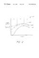
- FIG. 2illustrates the light output of power conversion circuits as a function of both current and temperature
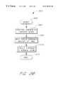
- FIG. 3Aillustrates the process for overdriving the lamp current based on lamp temperature
- FIG. 3Billustrates the process for overdriving the lamp current based on elapsed time
- FIG. 4is a schematic diagram of the power conversion circuit according to an embodiment of the present invention.
- FIG. 5is a schematic diagram of a portion of the power conversion circuit illustrating the amplitude and duty cycle control of the output signals of the PWM circuit.
- FIG. 6,comprising FIGS. 6A-6B, illustrates the voltage waveforms of the switching transistor drive signals generated by the PWM circuit of FIG. 4 .
- a power conversion circuit 3in accordance with a first embodiment of the present invention comprises integrators 16 , 18 , a controller 20 , a direct drive network 40 , a secondary network 60 , a CCFL 5 and a feedback circuit 80 .
- the CCFL 5provides illumination in an electronic device 10 , such as, for example, a flat panel display, a computer, a personal digital assistant, a palm top computer, a scanner, a facsimile machine, a copier, or the like.
- the integrators 16 , 18receives control signals in the form of either a digital pulse train or a DC waveform.
- the integratorsconvert the control signals into input signals comprising a DC voltage.
- the controller 20receives the DC voltage input signals from the integrators 16 , 18 .
- the controller 20is coupled to the direct drive network 40 which comprises a plurality of switching transistors coupled between the supply voltage VDD (e.g., 12V) and the ground in a full bridge topology.
- the control node (e.g., gate) of each transistoris coupled to the controller 20 to allow the controller 20 to control the switching of each transistor.
- the direct drive network 40also comprises a primary winding of a transformer which also has a secondary winding.
- the primary winding of the transformergenerally operates as an inductive circuit with some parasitic capacitance.
- the outputs of the transistorsare coupled directly to the primary winding without using any inductors and capacitors to tune the primary circuit to the operating frequency of the controller 20 .
- the primary winding of the direct drive network 40is magnetically coupled through a permeable core to a secondary network 60 .
- the secondary network 60comprises the secondary winding of the transformer, a reactive circuit element and a connector coupled to the CCFL 5 .
- the direct drive and secondary networksconvert the DC voltage coupled through the transistors into a substantially sinusoidal AC current.
- the sinusoidal AC currentpasses through the CCFL 5 to illuminate the CCFL 5 .
- the impedance of the direct drive network 40is largely inductive from the primary winding of the transformer with the capacitive reactance arising principally from the parasitic capacitances reflected from the secondary winding.
- the secondary network 60is coupled to a feedback circuit 80 which is also coupled to the controller 20 in order to provide a feedback signal to the controller 20 .
- the feedback circuit 80detects the total current passing through the CCFL 5 and generates a voltage signal representative of the total current.
- the feedback circuit 80may also be connected to a temperature sensor on the CCFL 5 .
- the temperature sensordetects the temperature of the CCFL 5 and generates a signal representative of the temperature of the CCFL 5 .
- the temperature sensor(not shown) is a thermistor mounted on the glass surface of the lamp.
- the feedback circuit 80provides the feedback voltage signal to the controller 20 so that the controller 20 can appropriately adjust the current passing through the CCFL 5 .
- FIG. 2illustrates the light output of typical lamps used in a backlight display environment.
- FIG. 2illustrates a graph 400 of the light output measured in candellas/meter 2 of various CCFL lamps as a function of temperature.
- the light output of the lampcan be viewed in three separate stages. At low temperatures, shown as Section A of the graph 400 , the light output of the lamp is generally low for a given current input. Section A of the graph 400 illustrates the light output of the lamp in cold temperatures before warm-up, and the temperature generally ranges from about ⁇ 40° C. to about 0° C.
- Section B of the graph 400illustrates the optimum temperature operating range for the lamp, with the lamp temperature generally ranging from about 50° C. to about 60° C. Eventually, the lamp reaches a temperature where the light output begins to decrease again, and this is illustrated in Section C of the graph 400 .
- the light outputbegins to decrease beginning at lamp temperatures above 70° C.
- the light output of a first lamp having a standard drive current of approximately 6 milliamperes (mA)is shown as line 405 of the graph 400 .
- mAmilliamperes
- Section Athe amount of light generated by the 6 mA of current flowing to the lamp is very low. This amount of light output is generally insufficient to provide adequate backlighting for a flat panel display.
- Section Bthe amount of light output by the lamp is illustrated by the portion of the line 405 in Section B.
- the light output in this sectionis within the recommended amount of light output for backlighted devices. If the lamp gets too warm, the light output actually decreases for the same 6 mA of current, as illustrated by the portion of the line 405 in Section C.
- the light output of a second lamp having a drive current of approximately 12 mAis shown as line 430 .
- a lampis overdriven when the lamp has a current above the normal operating range.
- the lampis overdriven when the current is in the range of above approximately 7 mA, and more preferably at approximately 12 mA.
- the low temperature portion of the line 430 as illustrated by Section Agenerates an increased amount of light as compared with the 6 mA lamp of the line 405 . This increased light output is generally sufficient to provide adequate backlighting for a flat panel display.
- the amount of light generated by the lampis illustrated by the portion of the line 430 in Section B.
- the light output during these conditionsis also increased as compared with the non-overdriven lamp shown in line 405 , but is also within the recommended amount of light output for backlighted devices.
- overdriving the lamp in this temperature rangeshortens the amount of time it takes the lamp to further heat and begin operating in the temperature range illustrated by portion of the line 430 in Section C.
- overdriving the lamp at a warm temperaturemay damage the lamp and shorten the overall life of the lamp.
- the performance of the lampis indicated by the portion of the line 430 in Section C. During this condition, the light output actually decreases for the same 12 mA of current.
- the light output of a third, self-heating lamp having a drive current of approximately 12 mAis shown as line 450 .
- the self-heating lampcontains two distinct gases, one optimized to operate at low temperatures and a second optimized to operate at normal to high temperatures. With the overdrive current flowing through the self-heating lamp during low temperatures, the amount of lamp light output is increased as compared to the standard 12 mA lamp shown in the line 430 .
- the low temperature gasis illuminating the lamp. After the lamp heats up, the amount of light output by the lamp is illustrated by the portion of the line 450 in Section B. During this portion of the line 450 , the lamp is illuminated by the higher temperature gas and the low temperature gas.
- the light output in this sectionis also increased as compared with the non-overdriven lamp shown in line 405 , but is also within the recommended amount of light output for backlight devices.
- overdriving the self-heating lamp at this pointalso shortens the amount of time it takes the lamp to further heat to the point that it is operating in the range illustrated by the portion of the line 450 in Section C, and overdriving may shorten the overall life of the lamp.
- the performance of the lampis indicated by the portion of the line 450 in Section C. During this condition, the light output decreases for the same 12 mA of current.
- a lampis overdriven at low temperature to provide an increased amount of light at start up. After the lamp warms up, the amount of current is reduced to maintain a high level of light output while preventing damage to the lamp.
- the present inventionprovides precise control of the lamp current as either a function of temperature or time. The steps for achieving this control are illustrated in FIGS. 3A and 3B.
- FIG. 3Aillustrates a process 500 used to control the amount of lamp current as a function of temperature.
- the processbegins at a start state 505 . Proceeding to an active state 510 , the controller 20 instructs the direct drive network 40 and the secondary network 60 to provide the lamp 5 with an overdrive current level of approximately 12 mA. As stated above, at low temperatures, the overdrive current provides an increased light output without damaging the lamp.
- the temperature of the lampis detected. This may be accomplished by installing a resistance temperature device (RTD) or other temperature detector to the lamp. This information is advantageously provided to the controller 20 as part of the feedback circuit 80 .
- the RTDmay be installed directly on the lamp or proximate the lamp.
- the controller 20determines whether the temperature has exceeded a predetermined threshold.
- This thresholdmay typically be set based upon the lamp operating characteristics to be a temperature at a transition between Section A and Section B in FIG. 2 . This ensures the overdrive current is provided during the entire low temperature range. If the temperature has not exceeded the threshold, the process 500 proceeds along the NO branch back to the state 515 to redetect the lamp temperature. The process 500 remains in this loop until the threshold lamp temperature is reached.
- the processproceeds along the YES branch to a state 525 .
- the current levelis reduced to a normal operating level of approximately 6 ma. This reduces the risk of damaging the lamp by overdriving a warm lamp. However, because the lamp is warm, the reduced level of current flow still provides adequate light output.
- the process 500then terminates in an end state 530 .
- the controller 20may also create a table to adjust the current flow as a function of temperature. For example, the current may be slowly decreased as the lamp warms according to the following table:
- FIG. 3Billustrates an alternate embodiment of the invention where the amount of lamp current is controlled as a function of time.
- the performance characteristics of a particular lamphave been predetermined. Based upon these characteristics, it can be determined the appropriate amount of time it takes the lamp to warm. Instead of detecting the lamp temperature, the controller overdrives the lamp current for this time interval.
- a process 550 based upon timebegins at a start state 555 . Proceeding to a decision state 560 , the controller 20 instructs the power conversion circuit to provide the lamp 5 with an overdrive current level of approximately 12 mA. As stated above, at low temperatures, the overdrive current provides an increased light output without damaging the lamp 5 .
- the controller 20waits a predetermined time interval.
- the time intervalmay be preselected based upon the warming characteristics of the lamp.
- the time required for any particular lamp to warm upmay be pre-programmed into the controller 20 .
- the circuitdoes not need a RTD or any temperature indications in the feedback circuit 80 .
- the process 550proceeds to an active state 570 .
- the current levelis reduced to a normal operating level of approximately 6 mA. This reduces the risk of damaging the lamp by overdriving a warm lamp. However, because the lamp is warm, the reduced level of current flow still provides adequate light output.
- the process 550then terminates in an end state 575 .
- the present inventionpermits dimming of the CCFL 5 using either amplitude current control, duty cycle current control, or a combination of amplitude and duty cycle current control.
- lampsare dimmed using only amplitude control.
- amplitude controllimits the range of dimming to only a factor of 3.
- duty cycle controlBy using duty cycle control, the full amplitude of the current is maintained so the lamp remains lit.
- the range of dimmingcan be increased to a factor of 100.
- FIG. 4illustrates an embodiment of the present invention in which two transistors drive the primary winding of the transformer.
- FIG. 4illustrates a drive circuit 800 which comprises a pulse width modulation (PWM) circuit 802 , a fist switching transistor 804 , a second switching transistor 806 , a transformer 808 , a DC blocking capacitor 810 , a first voltage divider capacitor 812 , a second voltage divider capacitor 814 , a first diode 818 , a second diode 820 , a current sensing resistor 822 and a current sensing filter capacitor 824 .
- the cold cathode fluorescent lamp (CCFL) 5is connected to the drive circuit.
- the PWM controller 802is an LX1686 regulating pulse width modulator, available from Linfinity Microelectronics Inc. of Garden Grove, Calif., or an equivalent thereof available from a number of industry sources.
- the first switching transistor 804is an N-channel field-effect transistor (FET) which has a gate connected to a first output (O A ) of the PWM circuit 802 , which has a drain connected to ground and which has a source connected to a first terminal 830 of the primary of the transformer 808 .
- the second switching transistor 806is also an N-channel FET which has a gate connected to a second output (O B ) of the PWM circuit 802 , which has a drain connected to ground and which has a source connected to a second terminal 832 of the primary of the transformer 808 .
- the primary of the transformer 808has a centertap 834 to provide an upper winding primary 836 between the terminal 830 and the centertap 834 and to provide a lower primary winding 838 between the terminal 832 and the centertap 834 .
- the centertap 834is connected to a source (+V IN ) of DC power, which may vary from approximately 8 volts to approximately 21 volts.
- a high voltage signal on the gate of the transistor 804 or on the gate of the transistor 806will turn on the respective transistor and provide a conductive path from the respective terminal of the primary winding, through the transistor to ground.
- the transistor 804conducts, and a current flows from the voltage source +V IN through the centertap 834 and the upper winding 836 to the terminal 830 .
- the transistor 806conducts, and a current flows from the voltage source +V IN through the centertap 834 and the lower winding 838 to the terminal 832 .
- a currentis caused to flow in the primary windings 836 , 838 , first in one direction from the centertap 834 through the upper winding 836 , and then in the opposite direction from the centertap 834 through the lower winding 838 .
- the signals O A and O Bare timed such that both signals are never active high at the same time.
- the transistors 804 , 806are turned on and off at a very high frequency. For example, in one particularly preferred embodiment, the transistors are turned on and off at a frequency of approximately 60 kHz.
- the transformer 808has a secondary winding 840 which has a first terminal 842 connected to ground and a second terminal 844 connected to a first terminal of the DC blocking capacitor 810 and to a first terminal of the first voltage divider capacitor 812 .
- a second terminal of the first voltage divider capacitor 812is connected to a node 846 .
- a first terminal of the second voltage divider capacitor 814is also connected to the node 846 .
- a second terminal of the second voltage divider capacitor 814is connected to ground.
- a sense voltageis developed on the node 846 .
- the node 846is connected via a line 848 to a voltage sense input (V S ) input of the PWM circuit 802 .
- the first voltage divider capacitor 812has a capacitance of approximately 1.3 picofarads
- the second voltage divider capacitor 814has a capacitance of approximately 470 picofarads.
- the sense voltage on the node 846will have a voltage which is approximately 0.3 percent of the voltage across the secondary winding 840 .
- the DC blocking capacitor 810couples the current generated in the secondary winding 840 to a first terminal 850 of the CCFL 5 .
- a second terminal 852 of the CCFL 5is coupled to the anode of the first diode 818 and to the cathode of the second diode 820 .
- the anode of the second diode 820is connected to ground.
- the anode of the first diode 818is connected to a first terminal of the current sensing resistor 822 .
- a second terminal of the current sensing resistor 822is connected to ground.
- the current sensing resistor 822has a value of approximately 953 ohms.
- the first diode 818operates as a half-wave rectifier such that a current sense voltage V I develops across the resistor 822 and the filter capacitor 824 responsive to the current through the CCFL 5 that flows from the terminal 844 of the secondary winding, through the DC blocking capacitor 810 , through the CCFL 5 , through the diode 818 and the resistor 822 to ground, and then to the terminal 842 .
- the current sense voltage V Iis provided as an input to a current sense input (I S ) of the PWM circuit 802 .
- the second diode 820provides a current path for the alternate half-cycles when the current flows out of the terminal 842 to ground, through the second diode 820 , through the CCFL 5 , through the DC blocking capacitor 810 and to the terminal 844 .
- the PWM circuit 802monitors the current via the current sense input I S and varies the pulse width modulation applied to the first and second switching transistors 804 , 806 . That is, if the sensed current is less than a desired current, then the transistors 804 , 806 are turned on for a greater duration in each cycle to increase the total current provided to the lamp 5 . Conversely, if the sensed current is greater than a desired current, then the transistors 804 , 806 are turned on for a shorter duration in each cycle to decrease the RMS current provided to the lamp 5 .
- the duty cycles of the transistors 804 , 806are varied, the switching frequency remains generally constant at approximately 60 kHz or at another selected high frequency. (Note, as discussed below, the transistors 804 , 806 may be turned completely off for time intervals not related to the switching frequency; however, when the transistors 804 , 806 are switching, the switching frequency remains generally constant.
- the first and second voltage divider capacitors 812 , 814provide an overvoltage protection circuit for the drive circuit 800 .
- the voltage applied to the V S input of the PWM circuit 802operates as a shutdown voltage to prevent the voltage across the secondary 840 of the transformer 808 from becoming to great.
- the voltage applied to the V S inputmay exceed a particular amount which is greater than approximately the voltage across two internal series connected diodes within the PWM circuit 802 .
- an internal signalis applied to the pulse width modulator within the PWM circuit to reduce the durations of the active signals generated at the outputs O A and O B , thus reducing the duration of the input currents applied to the primary windings 836 , 838 of the transformer 808 .
- the voltage across the secondary winding 840 of the transformer 808increases as the impedance of the CCFL 5 increases with age or if the CCFL 5 is disconnected or broken, the voltage provided by the voltage divider capacitors 812 , 814 limits the maximum voltage generated across the secondary winding 840 .
- the voltage from the voltage divider capacitors 812 , 814is applied to the V S input through a buffering circuit (not shown).
- the PWM circuit 802monitors the current flowing through the lamp 5 , compares the monitored current to a desired current, and varies the duty cycles of the two switching transistors 804 , 806 to maintain the monitored current approximately equal to the desired current.
- the brightness of the lamp 5may be varied by varying the desired current to which the monitored current is compared.
- the PWM circuit 802includes two inputs which control the desired current and thereby control the current provided to the lamp 5 .
- the PWM circuit 802includes a BRITE input and a BRT input.
- the BRITE input and the BRT inputare each responsive to a respective analog input voltage.
- the BRITE inputvaries a low frequency duty cycle (or burst cycle) of the desired current, and the BRT input varies the amplitude of the desired current.
- the two inputsoperate together to control the lamp current.
- the transistors 804 , 806are switched on and off at a frequency of approximately 60 kHz.
- the duty cycles of the transistors 804 , 806are varied to control the current in response to a comparison with a desired current.
- the desired currentis increased, the duration of the time that each transistor is on is increased; and if the desired current is decreased, the duration of the time that each transistor is on is decreased.
- the brightness of the lamp 5will vary accordingly; however, there is a limit to the amount of brightness control that can be obtained by varying current amplitude alone.
- the brightness of the lampcan also be adjusted by imposing a low frequency duty cycle on the desired current.
- the desired currentcan be controlled to a zero value (or some other low value) so that the transistors 804 , 806 are not turned on for any portion of high frequency cycles.
- This low frequency duty cycle controlis generally performed at a frequency of 90-300 Hz so that any flicker of the lamp 5 caused by turning the lamp on and off is not perceptible by the human eye.
- FIG. 5illustrates a portion of the internal circuitry of the pulse width modulation (PWM) circuit 802 which shows the interrelationship between the amplitude control and the duty cycle control of the lamp current.
- the illustrated portionimplements the brightness control using a combination of low frequency duty cycle control in response to the signal applied to the BRITE input and amplitude control in response to a signal applied to the BRT input.
- a DC voltage V BRITEreceived from the integrator 16 (FIGS. 1 and 4 ), is provided to the BRITE input of the PWM circuit 802 .
- the value of V BRITEcontrols the low frequency duty cycle of the output current.
- the V BRITE voltageis provided as the control input to a waveform generator 902 which is included within the PWM circuit 802 .
- the waveform generator 902is responsive to the DC voltage at the BRITE input to generate an output signal having an appropriate duty cycle.
- a value of V BRITE of approximately 0 voltsprovides an output signal having a 0% duty cycle and a value of V BRITE of approximately 2.5 volts provides an output signal with a 100% duty cycle.
- the duty cyclemay be varied between 0% and 100% by varying the value of V BRITE between 0 volts and 2.5 volts.
- the output signal from the waveform generator 902has a frequency of, for example, 90 Hz to 300 Hz.
- the output signal from the waveform generator 902is provided as the control input to a gate of a switching transistor 905 .
- the transistor 905is an N-channel FET which has a drain connected to a node 908 .
- the node 908is also connected to the output of a current source 910 , to the BRT input of the PWM circuit 602 and to a first terminal of a resistor 915 .
- a source of the transistor 905is connected to circuit ground.
- a second terminal of the resistor 915is also connected to ground.
- the current source 910provides a substantially constant current to the node 908 .
- the current from the current source 910flows through the resistor 915 and generates a voltage across the resistor 915 with respect to circuit ground.
- the voltage across the resistor 915is thus the voltage on the node 908 .
- the node voltageis provided as one input to a differential amplifier 930 .
- a second input to the differential amplifier 930is the current sense voltage V I .
- the differential amplifier 930compares the current sense voltage to the node voltage and provides an output voltage (PWM CONTROL) which varies in accordance with the difference between the two voltages.
- the output voltage from the differential amplifieris provided as the control input to the internal high frequency pulse (PWM) modulator 940 to control the duty cycle of the 60 kHz signal generated by the PWM modulator 940 so that the difference between the two voltages is minimized.
- PWMinternal high frequency pulse
- the transistor 905When the transistor 905 conducts, the current from the current source 910 is shunted to ground and bypasses the resistor 915 . Thus, the voltage across the resistor 910 is substantially zero, and therefore the node voltage applied to the differential amplifier 930 is substantially zero. This causes the differential amplifier 930 to output a PWM CONTROL voltage which causes both transistors 804 , 806 to have a substantially zero duty cycle during the time the transistor 905 is turned on. As discussed above, the duty cycle of the transistor 905 can be varied in accordance with the voltage V BRITE on the BRITE input. Thus, the switching voltage applied to the lamp 5 is modulated on and off at a low frequency in response to the voltage V BRITE . As further discussed above, the frequency of the low frequency modulation is sufficiently high (e.g., 90-300 Hz) that the on and off modulation of the lamp 5 is perceived as a difference in brightness rather than as flickering.
- the frequency of the low frequency modulationis sufficiently high (e.g., 90-
- the BRT input of the PWM circuit 802is also connected to the node 908 .
- the BRT inputreceives a voltage input V BRT from the integrator 18 (FIGS. 1 and 4) which determines the amplitude of the current to be generated by the PWM circuit 802 .
- the voltage input V BRTis provided by an output 952 of a differential amplifier 950 via a resistor 955 .
- the differential amplifier 950 and the resistor 955effectively operate as a variable current source.
- the current from the differential amplifier 950 via the resistor 955is supplied to the node 908 .
- this currentalso flows through the resistor 915 and increases the voltage across the resistor 915 accordingly.
- the output voltage from the differential amplifier 950is caused to vary from 1.25 volts to 2.5 volts.
- the resistor 955has a value of approximately 10,000 ohms.
- the current provided to the node 908 via the BRT inputvaries from approximately 0.125 mA to approximately 0.25 mA.
- the effect of changing V BRT and thus changing the current supplied to the BRT inputis to increase or decrease the node voltage when the transistor 905 is not conducting.
- V BRTdetermines the voltage to which the current sense voltage is compared during the active cycles of the PWM circuit 802 .
- the voltage V BRThas no effect on the inactive cycles when the transistor 905 is on because the current supplied to the node 908 is shunted by the transistor 905 along with the current from the current source 910 .
- the V BRITE signalis generated by the integrator 16
- the BRT signalis generated by the integrator 18 .
- the integrator 16 and the integrator 18are shown in more detail in FIG. 4 .
- the integrator 16receives a DUTYCTRL input signal and generates the V BRITE signal which controls the low frequency output duty cycle.
- the DUTYCTRL input signalmay be a digital pulse train or an analog signal (e.g., a DC signal).
- the integrator 16comprises resistors 702 , 704 , 706 , 710 , 712 , and 720 , capacitors 716 and 718 , and differential amplifiers 708 and 714 .
- the input signal DUTYCTRLis applied to a first terminal of the resistor 702 .
- a second terminal of the resistor 702is connected to an inverting input of the differential amplifier 708 and to a first terminal of the resistor 710 .
- a first terminal of the resistor 704is connected to a source voltage V DD .
- a first terminal of the resistor 706is connected to circuit ground.
- Respective second terminals of the resistors 704 and 706are connected together to form a voltage divider between the source voltage and ground. The two second terminals are connected to a non-inverting input of the differential amplifier 708 and to a non-inverting input of the differential amplifier 714 .
- An output of the differential amplifier 714is connected to a second terminal of the resistor 710 and to a first terminal of the resistor 712 .
- a second terminal of the resistor 712is connected to an inverting input of the differential amplifier 714 , to a first terminal of the capacitor 716 , to a first terminal of the capacitor 718 , and to a first terminal of the resistor 720 .
- An output of the differential amplifier 714is connected to a second terminal of the capacitor 716 , to the second terminal of the capacitor 718 , to a second terminal of the resistor 720 .
- the output of the differential amplifier 714is the V BRITE signal which is applied to the BRITE input of the PWM circuit 802 .
- the voltage divider provided by the resistors 704 and 706applies a constant DC voltage to the non-inverting inputs of the differential amplifiers 708 and 714 .
- the resistor 704has a resistance approximately three times the resistance of the resistor 706 (e.g., 18.7 Kohms versus 6.04 Kohms).
- V DDis approximately 5 volts
- the voltage applied to the non-inverting inputs of the two differential amplifiers 708 , 714is approximately 1.25 volts.
- the resistors 702 and 710configure the differential amplifier 708 as a clamped analog inverter.
- the differential amplifieris a LM324 amplifier available from National Semiconductor or an equivalent thereof which produces output signals between ground and a high state (e.g., V DD -1.5V).
- the resistors 702 and 710are identical (e.g., approximately 499 Kohm each) so that the differential amplifier 708 inverts the input signal and produces an output signal that varies between 2.5 volts and ground. This has the effect of clamping the output signal.
- the DUTYCTRL input signalis a DC voltage of 0 volts
- the voltage at the output of the differential amplifier 708is 2.5 volts, creating a voltage difference from the DUTYCTRL input to the differential amplifier 708 output of 2.5 volts.
- This 2.5 voltsis divided across the resistors 702 and 710 to produce 1.25 volts at the inverting input of the differential amplifier 708 , equaling the voltage at the non-inverting input.
- the DUTYCTRL input signalis a DC voltage of 2.5 volts
- the voltage at the output of the differential amplifier 708is 0 volts, creating a voltage difference from the DUTYCTRL input to the differential amplifier 708 output of 2.5 volts.
- This 2.5 voltsis divided across the resistors 702 and 710 to produce 1.25 volts at the inverting input of the differential amplifier 708 , equaling the voltage at the non-inverting input. Because the differential amplifier 708 cannot be driven below ground, a DUTYCTRL input signal of greater than 2.5 volts still results in 0 volts at the output.
- the voltage at the output of the differential amplifier 708is provided as an input to the inverting input of the differential amplifier 714 .
- the voltage applied to the non-inverting input of the differential amplifier 714is 1.25 volts.
- the differential amplifier 714operates in the same manner as the differential amplifier 708 , but the input voltage to the inverting input is limited by the output of the differential amplifier 708 to be in the range of 0-2.5 volts. Therefore, when the DUTYCTRL input is 0 volts, the output of the differential amplifier 708 is 2.5 volts, which results in the output of the differential amplifier being 0 volts.
- the inverter 16effectively passes a DC voltage input signal at the DUTYCTRL input to the BRITE input of the PWM circuit 802 , but clamps the output voltage at 2.5 volts.
- the integrator 16also coverts a digital pulse train signal into a DC voltage to be used as an input to the PWM circuit 802 . If the DUTYCTRL input is a digital pulse train, the differential amplifier 708 inverts and clamps the digital pulse train signal. For example, if a digital pulse train signal having an amplitude of 5 volts with a 75% duty cycle is applied to the DUTYCTRL input, the output of the differential amplifier is a digital pulse train signal having an amplitude of 2.5 volts with a 25% duty cycle. This signal is then input to the differential amplifier 714 , which in combination with resistors 712 , 720 and capacitors 716 , 718 integrates the digital pulse train signal.
- the output of the differential amplifier 714is a voltage having an average value substantially proportional to the duty cycle of the DUTYCTRL input signal. For example, for a 75% duty cycle, the output voltage is approximately 1.875 volts (0.75*2.5 volts). As a further example, a DUTYCTRL input signal having a 50% duty cycle would result in an output of the differential amplifier 714 of approximately 1.25 volts. A DUTYCTRL input signal having a 25% duty cycle would result in an output of the differential amplifier 714 of approximately 0.625 volts. Therefore, the integrator 16 creates a DC voltage (V BRITE ) that is proportional to the duty cycle of the DUTYCTRL input signal.
- V BRITEDC voltage
- the second integrator 18receives a AMPLCTRL input signal and generates the V BRT input signal which controls the amplitude of the output.
- the AMPLCTRL input signalmay be a digital pulse train or an analog signal.
- the integrator 18comprises resistors 730 , 732 , 734 , 736 , 740 , 742 , 748 , and 955 , a capacitor 746 , and differential amplifiers 738 and 950 , which are advantageously LM324 differential amplifiers.
- the integrator 18receives an input signal AMPLCTRL to control the output current amplitude.
- the input signal AMPLCTRLis applied to a first terminal of the resistor 730 .
- a second terminal of the resistor 730is connected to the inverting input of the differential amplifier 738 and to a first terminal of the resistor 740 .
- the non-inverting input of the differential amplifier 708is connected to a first terminal of the resistor 734 and to the first terminal of the resistor 736 .
- a second terminal of the resistor 734is connected to a first terminal of the resistor 732 and to the non-inverting input of the differential amplifier 950 .
- a second terminal of the resistor 732is connected to a source voltage V DD .
- the second terminal of the resistor 736is connected to ground.
- the output of the differential amplifier 738is connected to a second terminal of the resistor 740 and to a first terminal of the resistor 742 .
- the second terminal of the resistor 742is connected to the inverting input of the differential amplifier 950 , to a first terminal of the capacitor 746 , and to a first terminal of the resistor 748 .
- the output of the differential amplifier 950is connected to a second terminal of the capacitor 746 , to a second terminal of the resistor 748 , and to a first terminal of the resistor 955 .
- a second terminal of the resistor 955is connected to the BRT input of the PWM circuit 802 .
- the integrator 18converts a digital pulse train signal or analog waveform from the AMPLCTRL input into a DC voltage in the same manner as the integrator 16 . However, the integrator 18 offsets the AMPLCTRL input by a predetermined voltage.
- the voltage divider provided by the resistors 732 , 734 , and 736applies a constant DC voltage to the non-inverting inputs of the differential amplifiers 738 and 950 .
- the resistor 732has a resistance approximately six times the resistance of the resistors 734 and 736 (e.g., 18.7 Kohms versus 3.01 Kohms).
- the voltage applied to the non-inverting input of the differential amplifier 950is the voltage at a node 733 .
- the voltage at the node 733is approximately one-fourth the V DD voltage.
- V DDis approximately 5 volts
- the voltage applied to the non-inverting input of the differential amplifier 950is approximately 1.25 volts.
- the voltage applied to the non-inverting input of the differential amplifier 738is the voltage at a node 735 .
- the resistors 734 and 736are equal, the voltage at the node 735 is approximately one-half the voltage at the node 733 .
- V DDis approximately 5 volts
- the voltage applied to the non-inverting input of the differential amplifier 738is approximately 0.625 volts.
- the resistors 730 and 740configure the differential amplifier 738 as a clamped analog inverter.
- the differential amplifiers 738 and 950are preferably LM324 amplifiers which generate outputs that include ground. This permits clamping of the input signal to zero volts.
- the resistors 730 and 740are identical (e.g., approximately 499 Kohm each) so that the differential amplifier 738 inverts and clamps the AMPLCTRL input signal without otherwise changing it's amplitude.
- the AMPLCTRL input signalis a DC voltage of 0 volts
- the voltage at the output of the differential amplifier 708is 1.25 volts, creating a voltage difference from the AMPLCTRL input to the differential amplifier 738 output of 1.25 volts.
- This 1.25 voltsis divided across the resistors 730 and 740 to produce 0.625 volts at the inverting input of the differential amplifier 738 , equaling the voltage at the non-inverting input.
- the AMPLCTRL input signalis a DC voltage of 1.25 volts
- the voltage at the output of the differential amplifier 738is 0 volts, creating a voltage difference from the DUTYCTRL input to the differential amplifier 738 output of 1.25 volts.
- This 1.25 voltsis divided across the resistors 730 and 740 to produce 0.625 volts at the inverting input of the differential amplifier 738 , equaling the voltage at the non-inverting input. Because the differential amplifier 738 cannot be driven below ground, an AMPLCTRL input signal of greater than 1.25 volts still results in 0 volts at the output.
- the voltage in the range of 0-1.25 volts at the output of the differential amplifier 738is then provided through the resistor 742 as an input to the inverting input of the differential amplifier 950 .
- the voltage applied to the non-inverting input of the differential amplifier 950is 1.25 volts.
- the differential amplifier 950operates similarly to the differential amplifier 738 , but the input voltage to the inverting input of the differential amplifier 950 is limited by the output of the differential amplifier 738 to be in the range of 0-1.25 volts. If the AMPLCTRL input signal is a DC voltage of 0 volts, then the voltage at the output of the differential amplifier 738 is 1.25 volts.
- the difference between this 1.25 volts and the output voltage of the differential amplifier 950is divided across the resistors 742 and 748 to be used as the input signal to the differential amplifier 950 .
- the resistors 742 and 748are identical (e.g., approximately 499 Kohm each) so that the voltage is evenly divided. Because the voltage at the non-inverting input of the differential amplifier is 1.25 volts, to achieve a matching 1.25 volts at the inverting input of the differential amplifier 950 , the voltage at the output of the differential amplifier 950 is 1.25 volts. If the AMPLCTRL input signal is a DC voltage of 1.25 volts, then the voltage at the output of the differential amplifier 738 is 0 volts.
- the difference between this 0 volts and the output voltage of the differential amplifier 950is divided across the resistors 742 and 748 to be used as the input signal to the differential amplifier 950 . Because the voltage at the non-inverting input of the differential amplifier is 1.25 volts, to achieve a matching 1.25 volts at the inverting input of the differential amplifier 950 , the voltage at the output of the differential amplifier 950 is 2.5 volts. Thus, the integrator 18 effectively offsets a DC voltage input signal at the AMPLCTRL input to the BRT input of the PWM circuit 802 , but clamps the output voltage at 2.5 volts.
- the integrator 18also coverts a digital pulse train signal into a DC voltage to be used as an input to the PWM circuit 802 .
- the differential amplifier 738inverts and clamps the digital pulse train signal. For example, if a digital pulse train signal having an amplitude of 2.5 volts with a 75% duty cycle is applied to the AMPLCTRL input, the output of the differential amplifier 738 is a digital pulse train signal having an amplitude of 1.25 volts with a 25% duty cycle.
- This signalis then input to the differential amplifier 950 , which in combination with resistors 742 , 748 and capacitor 746 integrates the digital pulse train signal and offsets the output by 1.25 volts.
- the output of the differential amplifier 950is a DC voltage of approximately 2.1875 volts, which is greater than the baseline voltage of 1.25 volts by an amount approximately proportional to the AMPLCTRL input signal.
- an AMPLCTRL input signal having a 50% duty cycleresults in an output of the differential amplifier 950 of approximately 1.875 volts.
- An AMPLCTRL input signal having a 25% duty cycleresults in an output of the differential amplifier 950 of approximately 1.5625 volts.
- the value of the AMPLCTRL input and the DUTYCTRL inputis determined by a processor (not shown) or other circuitry based on the dimming level set.
- the processor or other circuitrymay adjust the value of the DUTYCTRL and AMPLCTRL input either independently or in combination to achieve the desired dimming level.
- the PWM circuit 802may control the brightness of the lamps 5 .
- the lamp 5may be overdriven in low temperatures, and dimmed throughout the temperature range using either duty cycle control, amplitude control, or a combination of the two. This provides a backlight system having the flexibility to operate over a large range of temperatures and brightness levels.
Landscapes
- Circuit Arrangements For Discharge Lamps (AREA)
Abstract
Description
| Temperature (° C.) | Current (mA) | ||
| −40 | 10 | ||
| −25 | 9 | ||
| −15 | 8 | ||
| 0 | 7 | ||
| 25 and higher | 6 | ||
Claims (53)
Priority Applications (1)
| Application Number | Priority Date | Filing Date | Title |
|---|---|---|---|
| US09/328,536US6198234B1 (en) | 1999-06-09 | 1999-06-09 | Dimmable backlight system |
Applications Claiming Priority (1)
| Application Number | Priority Date | Filing Date | Title |
|---|---|---|---|
| US09/328,536US6198234B1 (en) | 1999-06-09 | 1999-06-09 | Dimmable backlight system |
Publications (1)
| Publication Number | Publication Date |
|---|---|
| US6198234B1true US6198234B1 (en) | 2001-03-06 |
Family
ID=23281390
Family Applications (1)
| Application Number | Title | Priority Date | Filing Date |
|---|---|---|---|
| US09/328,536Expired - LifetimeUS6198234B1 (en) | 1999-06-09 | 1999-06-09 | Dimmable backlight system |
Country Status (1)
| Country | Link |
|---|---|
| US (1) | US6198234B1 (en) |
Cited By (85)
| Publication number | Priority date | Publication date | Assignee | Title |
|---|---|---|---|---|
| WO2002097548A1 (en)* | 2001-05-30 | 2002-12-05 | Accu-Sort Systems, Inc. | Amplitude control of gas discharge lamps |
| US20020180380A1 (en)* | 1999-07-22 | 2002-12-05 | Yung-Lin Lin | High-efficiency adaptive DC/AC converter |
| WO2003055280A1 (en)* | 2001-12-19 | 2003-07-03 | Northrop Grumman | Method and apparatus for dimming high-intensity fluorescent lamps |
| US20030160574A1 (en)* | 2002-02-26 | 2003-08-28 | Gray Richard L. | System and method for powering cold cathode fluorescent lighting |
| US20030161164A1 (en)* | 1998-12-11 | 2003-08-28 | Monolithic Power Systems, Inc. | Method and apparatus for controlling a discharge lamp in a backlighted display |
| US20030209960A1 (en)* | 2002-05-13 | 2003-11-13 | Delphi Technologies, Inc. | Heating element for fluorescent lamps |
| US6677710B2 (en) | 2002-02-28 | 2004-01-13 | Visteon Global Technologies, Inc. | DC output regulator using dual pulse modulation |
| US6690121B1 (en) | 2002-11-20 | 2004-02-10 | Visteon Global Technologies, Inc. | High precision luminance control for PWM-driven lamp |
| US20040032223A1 (en)* | 2002-06-18 | 2004-02-19 | Henry George C. | Square wave drive system |
| US20040056607A1 (en)* | 2002-06-18 | 2004-03-25 | Henry George C. | Lamp inverter with pre-regulator |
| US20040113569A1 (en)* | 2002-12-13 | 2004-06-17 | Henry George C. | Apparatus and method for striking a fluorescent lamp |
| US20040125062A1 (en)* | 1999-10-25 | 2004-07-01 | Tsunenori Yamamoto | Liquid crystal display apparatus |
| US6788597B2 (en)* | 2001-03-28 | 2004-09-07 | Micron Technology, Inc. | Memory device having programmable column segmentation to increase flexibility in bit repair |
| US20050013134A1 (en)* | 2003-05-31 | 2005-01-20 | Hyeong-Suk Yoo | Backlight assembly and liquid crystal display apparatus having the same |
| US20050017994A1 (en)* | 2003-07-26 | 2005-01-27 | Lg Electronics Inc. | Apparatus and method for controlling brightness level of display |
| US20050030776A1 (en)* | 1999-07-22 | 2005-02-10 | Yung-Lin Lin | High-efficiency adaptive DC/AC converter |
| US20050062436A1 (en)* | 2003-09-09 | 2005-03-24 | Xiaoping Jin | Split phase inverters for CCFL backlight system |
| US20050073266A1 (en)* | 2003-10-02 | 2005-04-07 | Moyer James Copland | Fixed operating frequency inverter for cold cathode fluorescent lamp having strike frequency adjusted by voltage to current phase relationship |
| US20050088102A1 (en)* | 2003-09-23 | 2005-04-28 | Ferguson Bruce R. | Optical and temperature feedbacks to control display brightness |
| US20050093484A1 (en)* | 2003-10-21 | 2005-05-05 | Ball Newton E. | Systems and methods for fault protection in a balancing transformer |
| US20050093472A1 (en)* | 2003-10-06 | 2005-05-05 | Xiaoping Jin | Balancing transformers for ring balancer |
| US20050099142A1 (en)* | 2003-11-12 | 2005-05-12 | Cottongim David E. | Thermal protection for lamp ballasts |
| US20050156539A1 (en)* | 2003-12-16 | 2005-07-21 | Ball Newton E. | Lamp current control using profile synthesizer |
| US20050174818A1 (en)* | 2004-02-11 | 2005-08-11 | Yung-Lin Lin | Liquid crystal display system with lamp feedback |
| US20050190142A1 (en)* | 2004-02-09 | 2005-09-01 | Ferguson Bruce R. | Method and apparatus to control display brightness with ambient light correction |
| US20050190171A1 (en)* | 2003-12-19 | 2005-09-01 | Hyeon-Yong Jang | Display device and device of driving light source therefor |
| US6946806B1 (en) | 2000-06-22 | 2005-09-20 | Microsemi Corporation | Method and apparatus for controlling minimum brightness of a fluorescent lamp |
| US20050218825A1 (en)* | 2004-04-01 | 2005-10-06 | Chii-Fa Chiou | Full-bridge and half-bridge compatible driver timing schedule for direct drive backlight system |
| US20050225256A1 (en)* | 2003-10-01 | 2005-10-13 | Scolaro Martin S | Method and apparatus for lamp heat control |
| US20050225261A1 (en)* | 2004-04-07 | 2005-10-13 | Xiaoping Jin | Primary side current balancing scheme for multiple CCF lamp operation |
| US20050248294A1 (en)* | 2004-05-10 | 2005-11-10 | Koito Manufacturing Co., Ltd. | Vehicular lamp |
| US20060001915A1 (en)* | 2004-06-22 | 2006-01-05 | Ching-Chung Chang | Warm-up circuit for CCFLs |
| US20060007107A1 (en)* | 2004-06-07 | 2006-01-12 | Ferguson Bruce R | Dual-slope brightness control for transflective displays |
| US20060012312A1 (en)* | 2004-07-19 | 2006-01-19 | Intersil Americas Inc. | Phase shift modulation-based control of amplitude of AC voltage output produced by double-ended DC-AC converter circuitry for powering high voltage load such as cold cathode fluorescent lamp |
| US20060017406A1 (en)* | 2004-07-26 | 2006-01-26 | Ball Newton E | Push-pull driver with null-short feature |
| US20060017404A1 (en)* | 2004-07-22 | 2006-01-26 | Hyeon-Yong Jang | Display device and driving device for a light source |
| US20060038502A1 (en)* | 2004-08-20 | 2006-02-23 | Moyer James C | Minimizing bond wire power losses in integrated circuit full bridge CCFL drivers |
| US20060049959A1 (en)* | 2003-02-06 | 2006-03-09 | Jorge Sanchez | Digital control system for lcd backlights |
| US20060077700A1 (en)* | 2002-04-24 | 2006-04-13 | O2 International Limited | High-efficiency adaptive DC/AC converter |
| US20060098935A1 (en)* | 2004-11-10 | 2006-05-11 | Yu Chung-Che | Pulse width modulation inverter circuit and control method thereof |
| US7061183B1 (en) | 2005-03-31 | 2006-06-13 | Microsemi Corporation | Zigzag topology for balancing current among paralleled gas discharge lamps |
| US20060145635A1 (en)* | 2005-01-03 | 2006-07-06 | Shin Chung-Hyuk | Lamp driving apparatus, liquid crystal display comprising the same, and driving method thereof |
| US20060158136A1 (en)* | 2005-01-19 | 2006-07-20 | Monolithic Power Systems, Inc. | Method and apparatus for DC to AC power conversion for driving discharge lamps |
| US20060170378A1 (en)* | 2005-01-31 | 2006-08-03 | Intersil Americas Inc. | DC-AC converter having phase-modulated, double-ended, full-bridge topology for powering high voltage load such as cold cathode fluorescent lamp |
| US20060170371A1 (en)* | 2005-01-31 | 2006-08-03 | Intersil Americas Inc. | DC-AC converter having phase-modulated, double-ended, half-bridge topology for powering high voltage load such as cold cathode fluorescent lamp |
| US20060186833A1 (en)* | 2005-02-23 | 2006-08-24 | Yu Chung-Che | Fluorescent tube driver circuit system of pulse-width modulation control |
| US20060220593A1 (en)* | 2005-03-31 | 2006-10-05 | Ball Newton E | Nested balancing topology for balancing current among multiple lamps |
| US20060221644A1 (en)* | 2005-03-30 | 2006-10-05 | Samsung Electronics Co., Ltd. | Backlight assembly and display device having the same |
| US20060220594A1 (en)* | 2005-03-29 | 2006-10-05 | Zippy Technology Corp. | Method for controlling an inverter under altering voltage |
| US20060255751A1 (en)* | 2003-11-12 | 2006-11-16 | Lutron Electronics Co., Inc. | Thermal protection for lamp ballasts |
| US20060261748A1 (en)* | 2004-07-28 | 2006-11-23 | Yasuhiro Nukisato | Discharge lamp ballast apparatus |
| US20060261750A1 (en)* | 2005-05-19 | 2006-11-23 | Lite-On Technology Corporation | Method and device for driving CCFL circuit |
| DE102005025682A1 (en)* | 2005-06-03 | 2006-12-07 | Minebea Co., Ltd., Kitasaku | Device for controlling fluorescent lamps in a lighting arrangement |
| US20070007908A1 (en)* | 2005-07-06 | 2007-01-11 | Monolithic Power Systems, Inc. | Current balancing technique with magnetic integration for fluorescent lamps |
| US20070018941A1 (en)* | 2003-11-03 | 2007-01-25 | Monolithic Power Systems, Inc. | Driver for light source having integrated photosensitive elements for driver control |
| US20070086217A1 (en)* | 2005-10-17 | 2007-04-19 | Monolithic Power System, Inc. | DC/AC convert for driving cold cathode fluorescent lamp |
| US20070085492A1 (en)* | 2005-10-13 | 2007-04-19 | Monolithic Power Systems, Inc. | Matrix inverter for driving multiple discharge lamps |
| EP1791109A1 (en)* | 2005-11-29 | 2007-05-30 | Sharp Kabushiki Kaisha | Liquid crystal display device |
| US20070236153A1 (en)* | 2006-04-11 | 2007-10-11 | Monolithic Power Systems, Inc. | Inverter for driving backlight devices in a large LCD panel |
| US20070247085A1 (en)* | 2006-04-19 | 2007-10-25 | Monolithic Power Systems, Inc. | Method and circuit for short-circuit and over-current protection in a discharge lamp system |
| US20070278971A1 (en)* | 2006-05-31 | 2007-12-06 | Monolithic Power Systems, Inc. | System and method for open lamp protection |
| US20080048584A1 (en)* | 2003-07-30 | 2008-02-28 | Lutron Electronics, Co., Inc. | System and method for reducing flicker of compact gas discharge lamps at low lamp light output level |
| US20080067952A1 (en)* | 2006-09-14 | 2008-03-20 | Cheng Ron Chan | DC digital starting device |
| US7355354B2 (en) | 1998-12-11 | 2008-04-08 | Monolithic Power Systems, Inc. | Method for starting a discharge lamp using high energy initial pulse |
| US20080084196A1 (en)* | 2006-10-04 | 2008-04-10 | Microsemi Corporation | Method and apparatus to compensate for supply voltage variations in a pwm-based voltage regulator |
| US7394203B2 (en) | 2005-12-15 | 2008-07-01 | Monolithic Power Systems, Inc. | Method and system for open lamp protection |
| US7414371B1 (en) | 2005-11-21 | 2008-08-19 | Microsemi Corporation | Voltage regulation loop with variable gain control for inverter circuit |
| US7420829B2 (en) | 2005-08-25 | 2008-09-02 | Monolithic Power Systems, Inc. | Hybrid control for discharge lamps |
| US7423384B2 (en) | 2005-11-08 | 2008-09-09 | Monolithic Power Systems, Inc. | Lamp voltage feedback system and method for open lamp protection and shorted lamp protection |
| US20080231916A1 (en)* | 2007-03-23 | 2008-09-25 | Takanori Inadome | Image reading device and image forming apparatus |
| US20080238864A1 (en)* | 2007-03-30 | 2008-10-02 | Innocom Technology (Shenzhen) Co., Ltd. | Light emitting diode driving circuit and liquid crystal display using same |
| US20080266311A1 (en)* | 2007-04-30 | 2008-10-30 | Duncan Cameron C | Computing device entertainment mode system and method |
| US20090140655A1 (en)* | 2007-11-29 | 2009-06-04 | Monolithic Power Systems, Inc. | Simple protection circuit and adaptive frequency sweeping method for ccfl inverter |
| EP1729281A3 (en)* | 2005-06-01 | 2009-07-22 | Samsung Electronics Co., Ltd. | Display apparatus and control method thereof |
| US7569998B2 (en) | 2006-07-06 | 2009-08-04 | Microsemi Corporation | Striking and open lamp regulation for CCFL controller |
| US7579787B2 (en) | 2004-10-13 | 2009-08-25 | Monolithic Power Systems, Inc. | Methods and protection schemes for driving discharge lamps in large panel applications |
| US20090273304A1 (en)* | 2008-05-01 | 2009-11-05 | Matsushita Electric Works, Ltd. | Apparatus and method for trimming an output parameter of an electronic ballast |
| EP1705964A3 (en)* | 2005-03-22 | 2010-01-27 | Patent-Treuhand-Gesellschaft für elektrische Glühlampen mbH | Ballast with dimmer |
| US20110084980A1 (en)* | 2009-10-08 | 2011-04-14 | Byoung-Gwan Lee | Liquid crystal display device and method of driving the same |
| US7977888B2 (en) | 2003-10-06 | 2011-07-12 | Microsemi Corporation | Direct coupled balancer drive for floating lamp structure |
| US8093839B2 (en) | 2008-11-20 | 2012-01-10 | Microsemi Corporation | Method and apparatus for driving CCFL at low burst duty cycle rates |
| US8598795B2 (en) | 2011-05-03 | 2013-12-03 | Microsemi Corporation | High efficiency LED driving method |
| US8754581B2 (en) | 2011-05-03 | 2014-06-17 | Microsemi Corporation | High efficiency LED driving method for odd number of LED strings |
| US9030119B2 (en) | 2010-07-19 | 2015-05-12 | Microsemi Corporation | LED string driver arrangement with non-dissipative current balancer |
| US20190036456A1 (en)* | 2016-01-05 | 2019-01-31 | Redisem Ltd. | Power control circuit |
Citations (35)
| Publication number | Priority date | Publication date | Assignee | Title |
|---|---|---|---|---|
| US4053813A (en) | 1976-03-01 | 1977-10-11 | General Electric Company | Discharge lamp ballast with resonant starting |
| US4307441A (en) | 1980-07-28 | 1981-12-22 | United Technologies Corporation | Current balanced DC-to-DC converter |
| US4453522A (en) | 1980-04-28 | 1984-06-12 | Stanadyne, Inc. | Apparatus for adjusting the timing of a fuel injection pump |
| US4480201A (en) | 1982-06-21 | 1984-10-30 | Eaton Corporation | Dual mode power transistor |
| US4555673A (en) | 1984-04-19 | 1985-11-26 | Signetics Corporation | Differential amplifier with rail-to-rail input capability and controlled transconductance |
| US4585974A (en) | 1983-01-03 | 1986-04-29 | North American Philips Corporation | Varible frequency current control device for discharge lamps |
| US4626770A (en) | 1985-07-31 | 1986-12-02 | Motorola, Inc. | NPN band gap voltage reference |
| US4682080A (en) | 1984-08-17 | 1987-07-21 | Hitachi, Ltd. | Discharge lamp operating device |
| US4779037A (en) | 1987-11-17 | 1988-10-18 | National Semiconductor Corporation | Dual input low dropout voltage regulator |
| US4792747A (en) | 1987-07-01 | 1988-12-20 | Texas Instruments Incorporated | Low voltage dropout regulator |
| US4812781A (en) | 1987-12-07 | 1989-03-14 | Silicon General, Inc. | Variable gain amplifier |
| US4885486A (en) | 1987-12-21 | 1989-12-05 | Sundstrand Corp. | Darlington amplifier with high speed turnoff |
| US5083065A (en) | 1989-10-23 | 1992-01-21 | Nissan Motor Co., Ltd. | Lighting device for electric discharge lamp |
| US5130635A (en) | 1990-09-18 | 1992-07-14 | Nippon Motorola Ltd. | Voltage regulator having bias current control circuit |
| US5220272A (en) | 1990-09-10 | 1993-06-15 | Linear Technology Corporation | Switching regulator with asymmetrical feedback amplifier and method |
| US5235254A (en)* | 1990-04-23 | 1993-08-10 | Pi Electronics Pte. Ltd. | Fluorescent lamp supply circuit |
| US5289051A (en) | 1991-09-24 | 1994-02-22 | Siemens Aktiengesellschaft | Power MOSFET driver having auxiliary current source |
| US5327028A (en) | 1992-06-22 | 1994-07-05 | Linfinity Microelectronics, Inc. | Voltage reference circuit with breakpoint compensation |
| US5471130A (en) | 1993-11-12 | 1995-11-28 | Linfinity Microelectronics, Inc. | Power supply controller having low startup current |
| US5475285A (en) | 1992-07-17 | 1995-12-12 | Motorola, Inc. | Lamp circuit limited to a booster in which the power output decreases with increasing frequency |
| US5479337A (en) | 1993-11-30 | 1995-12-26 | Kaiser Aerospace And Electronics Corporation | Very low power loss amplifier for analog signals utilizing constant-frequency zero-voltage-switching multi-resonant converter |
| US5514947A (en) | 1995-01-31 | 1996-05-07 | National Semiconductor Corporation | Phase lead compensation circuit for an integrated switching regulator |
| US5528192A (en) | 1993-11-12 | 1996-06-18 | Linfinity Microelectronics, Inc. | Bi-mode circuit for driving an output load |
| US5552697A (en) | 1995-01-20 | 1996-09-03 | Linfinity Microelectronics | Low voltage dropout circuit with compensating capacitance circuitry |
| US5563501A (en) | 1995-01-20 | 1996-10-08 | Linfinity Microelectronics | Low voltage dropout circuit with compensating capacitance circuitry |
| US5608312A (en) | 1995-04-17 | 1997-03-04 | Linfinity Microelectronics, Inc. | Source and sink voltage regulator for terminators |
| US5612594A (en) | 1995-09-13 | 1997-03-18 | C-P-M Lighting, Inc. | Electronic dimming ballast feedback control scheme |
| US5615093A (en) | 1994-08-05 | 1997-03-25 | Linfinity Microelectronics | Current synchronous zero voltage switching resonant topology |
| US5619402A (en) | 1996-04-16 | 1997-04-08 | O2 Micro, Inc. | Higher-efficiency cold-cathode fluorescent lamp power supply |
| US5719474A (en)* | 1996-06-14 | 1998-02-17 | Loral Corporation | Fluorescent lamps with current-mode driver control |
| US5748460A (en) | 1995-01-11 | 1998-05-05 | Canon Kabushiki Kaisha | Power supply apparatus |
| US5818172A (en)* | 1994-10-28 | 1998-10-06 | Samsung Electronics Co., Ltd. | Lamp control circuit having a brightness condition controller having 2.sup.nrd and 4th current paths |
| US5854617A (en)* | 1995-05-12 | 1998-12-29 | Samsung Electronics Co., Ltd. | Circuit and a method for controlling a backlight of a liquid crystal display in a portable computer |
| US5886477A (en)* | 1997-05-27 | 1999-03-23 | Nec Corporation | Driver of cold-cathode fluorescent lamp |
| US5907742A (en)* | 1997-03-09 | 1999-05-25 | Hewlett-Packard Company | Lamp control scheme for rapid warmup of fluorescent lamp in office equipment |
- 1999
- 1999-06-09USUS09/328,536patent/US6198234B1/ennot_activeExpired - Lifetime
Patent Citations (35)
| Publication number | Priority date | Publication date | Assignee | Title |
|---|---|---|---|---|
| US4053813A (en) | 1976-03-01 | 1977-10-11 | General Electric Company | Discharge lamp ballast with resonant starting |
| US4453522A (en) | 1980-04-28 | 1984-06-12 | Stanadyne, Inc. | Apparatus for adjusting the timing of a fuel injection pump |
| US4307441A (en) | 1980-07-28 | 1981-12-22 | United Technologies Corporation | Current balanced DC-to-DC converter |
| US4480201A (en) | 1982-06-21 | 1984-10-30 | Eaton Corporation | Dual mode power transistor |
| US4585974A (en) | 1983-01-03 | 1986-04-29 | North American Philips Corporation | Varible frequency current control device for discharge lamps |
| US4555673A (en) | 1984-04-19 | 1985-11-26 | Signetics Corporation | Differential amplifier with rail-to-rail input capability and controlled transconductance |
| US4682080A (en) | 1984-08-17 | 1987-07-21 | Hitachi, Ltd. | Discharge lamp operating device |
| US4626770A (en) | 1985-07-31 | 1986-12-02 | Motorola, Inc. | NPN band gap voltage reference |
| US4792747A (en) | 1987-07-01 | 1988-12-20 | Texas Instruments Incorporated | Low voltage dropout regulator |
| US4779037A (en) | 1987-11-17 | 1988-10-18 | National Semiconductor Corporation | Dual input low dropout voltage regulator |
| US4812781A (en) | 1987-12-07 | 1989-03-14 | Silicon General, Inc. | Variable gain amplifier |
| US4885486A (en) | 1987-12-21 | 1989-12-05 | Sundstrand Corp. | Darlington amplifier with high speed turnoff |
| US5083065A (en) | 1989-10-23 | 1992-01-21 | Nissan Motor Co., Ltd. | Lighting device for electric discharge lamp |
| US5235254A (en)* | 1990-04-23 | 1993-08-10 | Pi Electronics Pte. Ltd. | Fluorescent lamp supply circuit |
| US5220272A (en) | 1990-09-10 | 1993-06-15 | Linear Technology Corporation | Switching regulator with asymmetrical feedback amplifier and method |
| US5130635A (en) | 1990-09-18 | 1992-07-14 | Nippon Motorola Ltd. | Voltage regulator having bias current control circuit |
| US5289051A (en) | 1991-09-24 | 1994-02-22 | Siemens Aktiengesellschaft | Power MOSFET driver having auxiliary current source |
| US5327028A (en) | 1992-06-22 | 1994-07-05 | Linfinity Microelectronics, Inc. | Voltage reference circuit with breakpoint compensation |
| US5475285A (en) | 1992-07-17 | 1995-12-12 | Motorola, Inc. | Lamp circuit limited to a booster in which the power output decreases with increasing frequency |
| US5471130A (en) | 1993-11-12 | 1995-11-28 | Linfinity Microelectronics, Inc. | Power supply controller having low startup current |
| US5528192A (en) | 1993-11-12 | 1996-06-18 | Linfinity Microelectronics, Inc. | Bi-mode circuit for driving an output load |
| US5479337A (en) | 1993-11-30 | 1995-12-26 | Kaiser Aerospace And Electronics Corporation | Very low power loss amplifier for analog signals utilizing constant-frequency zero-voltage-switching multi-resonant converter |
| US5615093A (en) | 1994-08-05 | 1997-03-25 | Linfinity Microelectronics | Current synchronous zero voltage switching resonant topology |
| US5818172A (en)* | 1994-10-28 | 1998-10-06 | Samsung Electronics Co., Ltd. | Lamp control circuit having a brightness condition controller having 2.sup.nrd and 4th current paths |
| US5748460A (en) | 1995-01-11 | 1998-05-05 | Canon Kabushiki Kaisha | Power supply apparatus |
| US5552697A (en) | 1995-01-20 | 1996-09-03 | Linfinity Microelectronics | Low voltage dropout circuit with compensating capacitance circuitry |
| US5563501A (en) | 1995-01-20 | 1996-10-08 | Linfinity Microelectronics | Low voltage dropout circuit with compensating capacitance circuitry |
| US5514947A (en) | 1995-01-31 | 1996-05-07 | National Semiconductor Corporation | Phase lead compensation circuit for an integrated switching regulator |
| US5608312A (en) | 1995-04-17 | 1997-03-04 | Linfinity Microelectronics, Inc. | Source and sink voltage regulator for terminators |
| US5854617A (en)* | 1995-05-12 | 1998-12-29 | Samsung Electronics Co., Ltd. | Circuit and a method for controlling a backlight of a liquid crystal display in a portable computer |
| US5612594A (en) | 1995-09-13 | 1997-03-18 | C-P-M Lighting, Inc. | Electronic dimming ballast feedback control scheme |
| US5619402A (en) | 1996-04-16 | 1997-04-08 | O2 Micro, Inc. | Higher-efficiency cold-cathode fluorescent lamp power supply |
| US5719474A (en)* | 1996-06-14 | 1998-02-17 | Loral Corporation | Fluorescent lamps with current-mode driver control |
| US5907742A (en)* | 1997-03-09 | 1999-05-25 | Hewlett-Packard Company | Lamp control scheme for rapid warmup of fluorescent lamp in office equipment |
| US5886477A (en)* | 1997-05-27 | 1999-03-23 | Nec Corporation | Driver of cold-cathode fluorescent lamp |
Cited By (210)
| Publication number | Priority date | Publication date | Assignee | Title |
|---|---|---|---|---|
| US7355354B2 (en) | 1998-12-11 | 2008-04-08 | Monolithic Power Systems, Inc. | Method for starting a discharge lamp using high energy initial pulse |
| US7443107B2 (en) | 1998-12-11 | 2008-10-28 | Monolithic Power Systems, Inc. | Method and apparatus for controlling a discharge lamp in a backlighted display |
| US20060007719A1 (en)* | 1998-12-11 | 2006-01-12 | Shannon John R | Method and apparatus for controlling a discharge lamp in a backlighted display |
| US7880397B2 (en) | 1998-12-11 | 2011-02-01 | Monolithic Power Systems, Inc. | Method for starting a discharge lamp using high energy initial pulse |
| US20030161164A1 (en)* | 1998-12-11 | 2003-08-28 | Monolithic Power Systems, Inc. | Method and apparatus for controlling a discharge lamp in a backlighted display |
| US7417382B2 (en) | 1999-07-22 | 2008-08-26 | O2Micro International Limited | High-efficiency adaptive DC/AC converter |
| US7881084B2 (en) | 1999-07-22 | 2011-02-01 | O2Micro International Limited | DC/AC cold cathode fluorescent lamp inverter |
| US20020180380A1 (en)* | 1999-07-22 | 2002-12-05 | Yung-Lin Lin | High-efficiency adaptive DC/AC converter |
| US20080246413A1 (en)* | 1999-07-22 | 2008-10-09 | O2Micro, Inc. | Dc/ac cold cathode fluorescent lamp inverter |
| US7515445B2 (en) | 1999-07-22 | 2009-04-07 | 02Micro International Limited | High-efficiency adaptive DC/AC converter |
| US20050030776A1 (en)* | 1999-07-22 | 2005-02-10 | Yung-Lin Lin | High-efficiency adaptive DC/AC converter |
| US8552930B2 (en)* | 1999-10-25 | 2013-10-08 | Hitachi Displays, Ltd. | Liquid crystal display apparatus |
| US20040125062A1 (en)* | 1999-10-25 | 2004-07-01 | Tsunenori Yamamoto | Liquid crystal display apparatus |
| US6946806B1 (en) | 2000-06-22 | 2005-09-20 | Microsemi Corporation | Method and apparatus for controlling minimum brightness of a fluorescent lamp |
| US6788597B2 (en)* | 2001-03-28 | 2004-09-07 | Micron Technology, Inc. | Memory device having programmable column segmentation to increase flexibility in bit repair |
| WO2002097548A1 (en)* | 2001-05-30 | 2002-12-05 | Accu-Sort Systems, Inc. | Amplitude control of gas discharge lamps |
| WO2003055280A1 (en)* | 2001-12-19 | 2003-07-03 | Northrop Grumman | Method and apparatus for dimming high-intensity fluorescent lamps |
| US6853153B2 (en) | 2002-02-26 | 2005-02-08 | Analog Microelectronics, Inc. | System and method for powering cold cathode fluorescent lighting |
| US20050146290A1 (en)* | 2002-02-26 | 2005-07-07 | Analog Microelectronics, Inc. | System and method for powering cold cathode fluorescent lighting |
| US20030160574A1 (en)* | 2002-02-26 | 2003-08-28 | Gray Richard L. | System and method for powering cold cathode fluorescent lighting |
| US6677710B2 (en) | 2002-02-28 | 2004-01-13 | Visteon Global Technologies, Inc. | DC output regulator using dual pulse modulation |
| US20060077700A1 (en)* | 2002-04-24 | 2006-04-13 | O2 International Limited | High-efficiency adaptive DC/AC converter |
| US7515446B2 (en) | 2002-04-24 | 2009-04-07 | O2Micro International Limited | High-efficiency adaptive DC/AC converter |
| US6833657B2 (en) | 2002-05-13 | 2004-12-21 | Delphi Technologies, Inc. | Heating element for fluorescent lamps |
| US20030209960A1 (en)* | 2002-05-13 | 2003-11-13 | Delphi Technologies, Inc. | Heating element for fluorescent lamps |
| US20040056607A1 (en)* | 2002-06-18 | 2004-03-25 | Henry George C. | Lamp inverter with pre-regulator |
| US7321200B2 (en) | 2002-06-18 | 2008-01-22 | Microsemi Corporation | Square wave drive system |
| US20060022612A1 (en)* | 2002-06-18 | 2006-02-02 | Henry George C | Square wave drive system |
| US6969958B2 (en) | 2002-06-18 | 2005-11-29 | Microsemi Corporation | Square wave drive system |
| US6876157B2 (en) | 2002-06-18 | 2005-04-05 | Microsemi Corporation | Lamp inverter with pre-regulator |
| US20040032223A1 (en)* | 2002-06-18 | 2004-02-19 | Henry George C. | Square wave drive system |
| US6690121B1 (en) | 2002-11-20 | 2004-02-10 | Visteon Global Technologies, Inc. | High precision luminance control for PWM-driven lamp |
| US20080024075A1 (en)* | 2002-12-13 | 2008-01-31 | Microsemi Corporation | Apparatus and method for striking a fluorescent lamp |
| US6979959B2 (en)* | 2002-12-13 | 2005-12-27 | Microsemi Corporation | Apparatus and method for striking a fluorescent lamp |
| US7411360B2 (en) | 2002-12-13 | 2008-08-12 | Microsemi Corporation | Apparatus and method for striking a fluorescent lamp |
| US20060038513A1 (en)* | 2002-12-13 | 2006-02-23 | Henry George C | Apparatus and method for striking a fluorescent lamp |
| US7279852B2 (en) | 2002-12-13 | 2007-10-09 | Microsemi Corporation | Apparatus and method for striking a fluorescent lamp |
| US20040113569A1 (en)* | 2002-12-13 | 2004-06-17 | Henry George C. | Apparatus and method for striking a fluorescent lamp |
| US7633233B2 (en)* | 2003-02-06 | 2009-12-15 | Jorge Sanchez | Digital control system for LCD backlights |
| US20060049959A1 (en)* | 2003-02-06 | 2006-03-09 | Jorge Sanchez | Digital control system for lcd backlights |
| US7159999B2 (en)* | 2003-05-31 | 2007-01-09 | Samsung Electronics Co., Ltd. | Backlight assembly and liquid crystal display apparatus having the same |
| US20050013134A1 (en)* | 2003-05-31 | 2005-01-20 | Hyeong-Suk Yoo | Backlight assembly and liquid crystal display apparatus having the same |
| US20050017994A1 (en)* | 2003-07-26 | 2005-01-27 | Lg Electronics Inc. | Apparatus and method for controlling brightness level of display |
| US7605829B2 (en)* | 2003-07-26 | 2009-10-20 | Lg Electronics Inc. | Apparatus and method for controlling brightness level of display |
| US7830093B2 (en)* | 2003-07-30 | 2010-11-09 | Lutron Electronics, Co., Inc. | System and method for reducing flicker of compact gas discharge lamps at low lamp light output level |
| US20080048584A1 (en)* | 2003-07-30 | 2008-02-28 | Lutron Electronics, Co., Inc. | System and method for reducing flicker of compact gas discharge lamps at low lamp light output level |
| US7187139B2 (en) | 2003-09-09 | 2007-03-06 | Microsemi Corporation | Split phase inverters for CCFL backlight system |
| US7952298B2 (en) | 2003-09-09 | 2011-05-31 | Microsemi Corporation | Split phase inverters for CCFL backlight system |
| US7525255B2 (en) | 2003-09-09 | 2009-04-28 | Microsemi Corporation | Split phase inverters for CCFL backlight system |
| US20050062436A1 (en)* | 2003-09-09 | 2005-03-24 | Xiaoping Jin | Split phase inverters for CCFL backlight system |
| US20070145911A1 (en)* | 2003-09-09 | 2007-06-28 | Microsemi Corporation | Split phase inverters for ccfl backlight system |
| US20090206767A1 (en)* | 2003-09-09 | 2009-08-20 | Microsemi Corporation | Split phase inverters for ccfl backlight system |
| US7391172B2 (en) | 2003-09-23 | 2008-06-24 | Microsemi Corporation | Optical and temperature feedbacks to control display brightness |
| US7183727B2 (en)* | 2003-09-23 | 2007-02-27 | Microsemi Corporation | Optical and temperature feedbacks to control display brightness |
| US20050088102A1 (en)* | 2003-09-23 | 2005-04-28 | Ferguson Bruce R. | Optical and temperature feedbacks to control display brightness |
| US20070132398A1 (en)* | 2003-09-23 | 2007-06-14 | Microsemi Corporation | Optical and temperature feedbacks to control display brightness |
| US7372210B2 (en)* | 2003-10-01 | 2008-05-13 | Snap-On Incorporated | Method and apparatus for lamp heat control |
| US20050225256A1 (en)* | 2003-10-01 | 2005-10-13 | Scolaro Martin S | Method and apparatus for lamp heat control |
| US20050140313A1 (en)* | 2003-10-02 | 2005-06-30 | Monolithic Power Systems, Inc. | Fixed operating frequency inverter for cold cathode fluorescent lamp having strike frequency adjusted by voltage to current phase relationship |
| US7294974B2 (en) | 2003-10-02 | 2007-11-13 | Monolithic Power Systems, Inc. | Fixed operating frequency inverter for cold cathode fluorescent lamp having strike frequency adjusted by voltage to current phase relationship |
| US20050073266A1 (en)* | 2003-10-02 | 2005-04-07 | Moyer James Copland | Fixed operating frequency inverter for cold cathode fluorescent lamp having strike frequency adjusted by voltage to current phase relationship |
| USRE44133E1 (en) | 2003-10-02 | 2013-04-09 | Monolithic Power Systems, Inc. | Fixed operating frequency inverter for cold cathode fluorescent lamp having strike frequency adjusted by voltage to current phase relationship |
| US6919694B2 (en) | 2003-10-02 | 2005-07-19 | Monolithic Power Systems, Inc. | Fixed operating frequency inverter for cold cathode fluorescent lamp having strike frequency adjusted by voltage to current phase relationship |
| US20090267521A1 (en)* | 2003-10-06 | 2009-10-29 | Microsemi Corporation | Balancing transformers for multi-lamp operation |
| US20050093472A1 (en)* | 2003-10-06 | 2005-05-05 | Xiaoping Jin | Balancing transformers for ring balancer |
| US7294971B2 (en) | 2003-10-06 | 2007-11-13 | Microsemi Corporation | Balancing transformers for ring balancer |
| US7242147B2 (en) | 2003-10-06 | 2007-07-10 | Microsemi Corporation | Current sharing scheme for multiple CCF lamp operation |
| US7990072B2 (en) | 2003-10-06 | 2011-08-02 | Microsemi Corporation | Balancing arrangement with reduced amount of balancing transformers |
| US7977888B2 (en) | 2003-10-06 | 2011-07-12 | Microsemi Corporation | Direct coupled balancer drive for floating lamp structure |
| US7560875B2 (en) | 2003-10-06 | 2009-07-14 | Microsemi Corporation | Balancing transformers for multi-lamp operation |
| US7932683B2 (en) | 2003-10-06 | 2011-04-26 | Microsemi Corporation | Balancing transformers for multi-lamp operation |
| US20050093471A1 (en)* | 2003-10-06 | 2005-05-05 | Xiaoping Jin | Current sharing scheme for multiple CCF lamp operation |
| US8222836B2 (en) | 2003-10-06 | 2012-07-17 | Microsemi Corporation | Balancing transformers for multi-lamp operation |
| US20110181204A1 (en)* | 2003-10-06 | 2011-07-28 | Microsemi Corporation | Balancing transformers for multi-lamp operation |
| US8008867B2 (en) | 2003-10-06 | 2011-08-30 | Microsemi Corporation | Arrangement suitable for driving floating CCFL based backlight |
| US7250726B2 (en) | 2003-10-21 | 2007-07-31 | Microsemi Corporation | Systems and methods for a transformer configuration with a tree topology for current balancing in gas discharge lamps |
| US20050093483A1 (en)* | 2003-10-21 | 2005-05-05 | Ball Newton E. | Systems and methods for a transformer configuration for driving multiple gas discharge tubes in parallel |
| US7141933B2 (en) | 2003-10-21 | 2006-11-28 | Microsemi Corporation | Systems and methods for a transformer configuration for driving multiple gas discharge tubes in parallel |
| US20050093484A1 (en)* | 2003-10-21 | 2005-05-05 | Ball Newton E. | Systems and methods for fault protection in a balancing transformer |
| US7279851B2 (en) | 2003-10-21 | 2007-10-09 | Microsemi Corporation | Systems and methods for fault protection in a balancing transformer |
| US20070018941A1 (en)* | 2003-11-03 | 2007-01-25 | Monolithic Power Systems, Inc. | Driver for light source having integrated photosensitive elements for driver control |
| US7436131B2 (en) | 2003-11-12 | 2008-10-14 | Lutron Electronics Co., Inc. | Thermal protection for lamp ballasts |
| US7675250B2 (en) | 2003-11-12 | 2010-03-09 | Lutron Electronics Co., Inc. | Thermal protection for lamp ballasts |
| CN1879457B (en)* | 2003-11-12 | 2010-04-28 | 卢特龙电子公司 | Thermal protection for lamp ballasts |
| US7911156B2 (en) | 2003-11-12 | 2011-03-22 | Lutron Electronics Co., Inc. | Thermal foldback for a lamp control device |
| US6982528B2 (en) | 2003-11-12 | 2006-01-03 | Lutron Electronics Co., Inc. | Thermal protection for lamp ballasts |
| US20050099142A1 (en)* | 2003-11-12 | 2005-05-12 | Cottongim David E. | Thermal protection for lamp ballasts |
| US20050280377A1 (en)* | 2003-11-12 | 2005-12-22 | Lutron Electronics Co., Inc. | Thermal protection for lamp ballasts |
| US20060255751A1 (en)* | 2003-11-12 | 2006-11-16 | Lutron Electronics Co., Inc. | Thermal protection for lamp ballasts |
| US20100171435A1 (en)* | 2003-11-12 | 2010-07-08 | Venkatesh Chitta | Thermal Protection For Lamp Ballasts |
| US7940015B2 (en) | 2003-11-12 | 2011-05-10 | Lutron Electronics Co., Inc. | Thermal protection for lamp ballasts |
| US20090033248A1 (en)* | 2003-11-12 | 2009-02-05 | Cottongim David E | Thermal Foldback For A Lamp Control Device |
| WO2005048660A1 (en) | 2003-11-12 | 2005-05-26 | Lutron Electronics Co., Inc. | Thermal protection for lamp ballasts |
| US7239087B2 (en) | 2003-12-16 | 2007-07-03 | Microsemi Corporation | Method and apparatus to drive LED arrays using time sharing technique |
| US7183724B2 (en) | 2003-12-16 | 2007-02-27 | Microsemi Corporation | Inverter with two switching stages for driving lamp |
| US20050156540A1 (en)* | 2003-12-16 | 2005-07-21 | Ball Newton E. | Inverter with two switching stages for driving lamp |
| US20050162098A1 (en)* | 2003-12-16 | 2005-07-28 | Ball Newton E. | Current-mode direct-drive inverter |
| US7265499B2 (en) | 2003-12-16 | 2007-09-04 | Microsemi Corporation | Current-mode direct-drive inverter |
| US7187140B2 (en) | 2003-12-16 | 2007-03-06 | Microsemi Corporation | Lamp current control using profile synthesizer |
| US20050156536A1 (en)* | 2003-12-16 | 2005-07-21 | Ball Newton E. | Method and apparatus to drive LED arrays using time sharing technique |
| US20050156539A1 (en)* | 2003-12-16 | 2005-07-21 | Ball Newton E. | Lamp current control using profile synthesizer |
| US20050190171A1 (en)* | 2003-12-19 | 2005-09-01 | Hyeon-Yong Jang | Display device and device of driving light source therefor |
| US20050190142A1 (en)* | 2004-02-09 | 2005-09-01 | Ferguson Bruce R. | Method and apparatus to control display brightness with ambient light correction |
| US8223117B2 (en) | 2004-02-09 | 2012-07-17 | Microsemi Corporation | Method and apparatus to control display brightness with ambient light correction |
| US7468722B2 (en) | 2004-02-09 | 2008-12-23 | Microsemi Corporation | Method and apparatus to control display brightness with ambient light correction |
| US20050174818A1 (en)* | 2004-02-11 | 2005-08-11 | Yung-Lin Lin | Liquid crystal display system with lamp feedback |
| US7394209B2 (en) | 2004-02-11 | 2008-07-01 | 02 Micro International Limited | Liquid crystal display system with lamp feedback |
| US7965046B2 (en) | 2004-04-01 | 2011-06-21 | Microsemi Corporation | Full-bridge and half-bridge compatible driver timing schedule for direct drive backlight system |
| US7646152B2 (en) | 2004-04-01 | 2010-01-12 | Microsemi Corporation | Full-bridge and half-bridge compatible driver timing schedule for direct drive backlight system |
| US20050218825A1 (en)* | 2004-04-01 | 2005-10-06 | Chii-Fa Chiou | Full-bridge and half-bridge compatible driver timing schedule for direct drive backlight system |
| US7112929B2 (en) | 2004-04-01 | 2006-09-26 | Microsemi Corporation | Full-bridge and half-bridge compatible driver timing schedule for direct drive backlight system |
| US20070014130A1 (en)* | 2004-04-01 | 2007-01-18 | Chii-Fa Chiou | Full-bridge and half-bridge compatible driver timing schedule for direct drive backlight system |
| US20100090611A1 (en)* | 2004-04-01 | 2010-04-15 | Microsemi Corporation | Full-bridge and half-bridge compatible driver timing schedule for direct drive backlight system |
| US20050225261A1 (en)* | 2004-04-07 | 2005-10-13 | Xiaoping Jin | Primary side current balancing scheme for multiple CCF lamp operation |
| US7557517B2 (en) | 2004-04-07 | 2009-07-07 | Microsemi Corporation | Primary side current balancing scheme for multiple CCF lamp operation |
| US7250731B2 (en) | 2004-04-07 | 2007-07-31 | Microsemi Corporation | Primary side current balancing scheme for multiple CCF lamp operation |
| US20050248294A1 (en)* | 2004-05-10 | 2005-11-10 | Koito Manufacturing Co., Ltd. | Vehicular lamp |
| US7208880B2 (en)* | 2004-05-10 | 2007-04-24 | Koito Manufacturing Co. Ltd. | Vehicular lamp |
| US20060007107A1 (en)* | 2004-06-07 | 2006-01-12 | Ferguson Bruce R | Dual-slope brightness control for transflective displays |
| US7755595B2 (en) | 2004-06-07 | 2010-07-13 | Microsemi Corporation | Dual-slope brightness control for transflective displays |
| US20060001915A1 (en)* | 2004-06-22 | 2006-01-05 | Ching-Chung Chang | Warm-up circuit for CCFLs |
| US7471427B2 (en)* | 2004-06-22 | 2008-12-30 | Lite-On Technology Corporation | Warm-up circuit for CCFLs |
| USRE43808E1 (en) | 2004-07-19 | 2012-11-20 | Intersil Americas Inc. | Phase shift modulation-based control of amplitude of AC voltage output produced by double-ended DC-AC converter circuitry for powering high voltage load such as cold cathode fluorescent lamp |
| US7368880B2 (en) | 2004-07-19 | 2008-05-06 | Intersil Americas Inc. | Phase shift modulation-based control of amplitude of AC voltage output produced by double-ended DC-AC converter circuitry for powering high voltage load such as cold cathode fluorescent lamp |
| US20060012312A1 (en)* | 2004-07-19 | 2006-01-19 | Intersil Americas Inc. | Phase shift modulation-based control of amplitude of AC voltage output produced by double-ended DC-AC converter circuitry for powering high voltage load such as cold cathode fluorescent lamp |
| US20060017404A1 (en)* | 2004-07-22 | 2006-01-26 | Hyeon-Yong Jang | Display device and driving device for a light source |
| US7595785B2 (en)* | 2004-07-22 | 2009-09-29 | Samsung Electronics Co., Ltd. | Display device and driving device for a light source |
| US20060017406A1 (en)* | 2004-07-26 | 2006-01-26 | Ball Newton E | Push-pull driver with null-short feature |
| US7173380B2 (en) | 2004-07-26 | 2007-02-06 | Microsemi Corporation | Push-pull driver with null-short feature |
| US20060261748A1 (en)* | 2004-07-28 | 2006-11-23 | Yasuhiro Nukisato | Discharge lamp ballast apparatus |
| US7298095B2 (en)* | 2004-07-28 | 2007-11-20 | Mitsubishi Denki Kabushiki Kaisha | Discharge lamp ballast apparatus |
| US7323829B2 (en) | 2004-08-20 | 2008-01-29 | Monolithic Power Systems, Inc. | Minimizing bond wire power losses in integrated circuit full bridge CCFL drivers |
| US20060038502A1 (en)* | 2004-08-20 | 2006-02-23 | Moyer James C | Minimizing bond wire power losses in integrated circuit full bridge CCFL drivers |
| US7579787B2 (en) | 2004-10-13 | 2009-08-25 | Monolithic Power Systems, Inc. | Methods and protection schemes for driving discharge lamps in large panel applications |
| US7242153B2 (en) | 2004-11-10 | 2007-07-10 | Beyond Innovation Technology Co., Ltd. | Pulse width modulation inverter circuit and control method thereof |
| US20060098935A1 (en)* | 2004-11-10 | 2006-05-11 | Yu Chung-Che | Pulse width modulation inverter circuit and control method thereof |
| US20060145635A1 (en)* | 2005-01-03 | 2006-07-06 | Shin Chung-Hyuk | Lamp driving apparatus, liquid crystal display comprising the same, and driving method thereof |
| US7511434B2 (en)* | 2005-01-03 | 2009-03-31 | Samsung Electronics Co., Ltd. | Lamp driving apparatus, liquid crystal display comprising the same, and driving method thereof |
| US20060158136A1 (en)* | 2005-01-19 | 2006-07-20 | Monolithic Power Systems, Inc. | Method and apparatus for DC to AC power conversion for driving discharge lamps |
| US7560879B2 (en) | 2005-01-19 | 2009-07-14 | Monolithic Power Systems, Inc. | Method and apparatus for DC to AC power conversion for driving discharge lamps |
| US7560872B2 (en) | 2005-01-31 | 2009-07-14 | Intersil Americas Inc. | DC-AC converter having phase-modulated, double-ended, half-bridge topology for powering high voltage load such as cold cathode fluorescent lamp |
| US20060170371A1 (en)* | 2005-01-31 | 2006-08-03 | Intersil Americas Inc. | DC-AC converter having phase-modulated, double-ended, half-bridge topology for powering high voltage load such as cold cathode fluorescent lamp |
| US20060170378A1 (en)* | 2005-01-31 | 2006-08-03 | Intersil Americas Inc. | DC-AC converter having phase-modulated, double-ended, full-bridge topology for powering high voltage load such as cold cathode fluorescent lamp |
| US7564193B2 (en) | 2005-01-31 | 2009-07-21 | Intersil Americas Inc. | DC-AC converter having phase-modulated, double-ended, full-bridge topology for powering high voltage load such as cold cathode fluorescent lamp |
| US20060186833A1 (en)* | 2005-02-23 | 2006-08-24 | Yu Chung-Che | Fluorescent tube driver circuit system of pulse-width modulation control |
| EP1705964A3 (en)* | 2005-03-22 | 2010-01-27 | Patent-Treuhand-Gesellschaft für elektrische Glühlampen mbH | Ballast with dimmer |
| CN1849030B (en)* | 2005-03-22 | 2011-05-25 | 电灯专利信托有限公司 | Ballast with dimmer |
| US20060220594A1 (en)* | 2005-03-29 | 2006-10-05 | Zippy Technology Corp. | Method for controlling an inverter under altering voltage |
| US7294975B2 (en)* | 2005-03-29 | 2007-11-13 | Zippy Technology Corp. | Method for controlling an inverter under altering voltage |
| US20060221644A1 (en)* | 2005-03-30 | 2006-10-05 | Samsung Electronics Co., Ltd. | Backlight assembly and display device having the same |
| US7061183B1 (en) | 2005-03-31 | 2006-06-13 | Microsemi Corporation | Zigzag topology for balancing current among paralleled gas discharge lamps |
| US7173382B2 (en) | 2005-03-31 | 2007-02-06 | Microsemi Corporation | Nested balancing topology for balancing current among multiple lamps |
| US20060220593A1 (en)* | 2005-03-31 | 2006-10-05 | Ball Newton E | Nested balancing topology for balancing current among multiple lamps |
| US7298093B2 (en)* | 2005-05-19 | 2007-11-20 | Lite-On Technology Corporation | Method and device for driving CCFL circuit |
| CN100581313C (en)* | 2005-05-19 | 2010-01-13 | 光宝科技股份有限公司 | Cold cathode fluorescent lamp circuit driving method and device and related electronic device |
| US20060261750A1 (en)* | 2005-05-19 | 2006-11-23 | Lite-On Technology Corporation | Method and device for driving CCFL circuit |
| EP1729281A3 (en)* | 2005-06-01 | 2009-07-22 | Samsung Electronics Co., Ltd. | Display apparatus and control method thereof |
| DE102005025682B4 (en)* | 2005-06-03 | 2010-04-22 | Minebea Co., Ltd., Kitasaku | Device for controlling fluorescent lamps in a lighting arrangement |
| US20060273743A1 (en)* | 2005-06-03 | 2006-12-07 | Minebea Co., Ltd. | Device for the control of fluorescent lamps in a lighting arrangement |
| US7397200B2 (en) | 2005-06-03 | 2008-07-08 | Minebea Co., Ltd. | Device for the control of fluorescent lamps in a lighting arrangement |
| DE102005025682A1 (en)* | 2005-06-03 | 2006-12-07 | Minebea Co., Ltd., Kitasaku | Device for controlling fluorescent lamps in a lighting arrangement |
| US7439685B2 (en) | 2005-07-06 | 2008-10-21 | Monolithic Power Systems, Inc. | Current balancing technique with magnetic integration for fluorescent lamps |
| US20070007908A1 (en)* | 2005-07-06 | 2007-01-11 | Monolithic Power Systems, Inc. | Current balancing technique with magnetic integration for fluorescent lamps |
| US7420829B2 (en) | 2005-08-25 | 2008-09-02 | Monolithic Power Systems, Inc. | Hybrid control for discharge lamps |
| US20070085492A1 (en)* | 2005-10-13 | 2007-04-19 | Monolithic Power Systems, Inc. | Matrix inverter for driving multiple discharge lamps |
| US7291991B2 (en) | 2005-10-13 | 2007-11-06 | Monolithic Power Systems, Inc. | Matrix inverter for driving multiple discharge lamps |
| US7825605B2 (en) | 2005-10-17 | 2010-11-02 | Monolithic Power Systems, Inc. | DA/AC convert for driving cold cathode fluorescent lamp |
| US20070086217A1 (en)* | 2005-10-17 | 2007-04-19 | Monolithic Power System, Inc. | DC/AC convert for driving cold cathode fluorescent lamp |
| US7423384B2 (en) | 2005-11-08 | 2008-09-09 | Monolithic Power Systems, Inc. | Lamp voltage feedback system and method for open lamp protection and shorted lamp protection |
| US7414371B1 (en) | 2005-11-21 | 2008-08-19 | Microsemi Corporation | Voltage regulation loop with variable gain control for inverter circuit |
| EP1791109A1 (en)* | 2005-11-29 | 2007-05-30 | Sharp Kabushiki Kaisha | Liquid crystal display device |
| US20070120505A1 (en)* | 2005-11-29 | 2007-05-31 | Sharp Kabushiki Kaisha | Liquid crystal display device |
| US7750582B2 (en) | 2005-11-29 | 2010-07-06 | Sharp Kabushiki Kaisha | Liquid crystal display device |
| US20080258651A1 (en)* | 2005-12-15 | 2008-10-23 | Monolithic Power Systems, Inc. | Method and system for open lamp protection |
| US7719206B2 (en) | 2005-12-15 | 2010-05-18 | Monolithic Power Systems, Inc. | Method and system for open lamp protection |
| US7394203B2 (en) | 2005-12-15 | 2008-07-01 | Monolithic Power Systems, Inc. | Method and system for open lamp protection |
| US7619371B2 (en) | 2006-04-11 | 2009-11-17 | Monolithic Power Systems, Inc. | Inverter for driving backlight devices in a large LCD panel |
| US20070236153A1 (en)* | 2006-04-11 | 2007-10-11 | Monolithic Power Systems, Inc. | Inverter for driving backlight devices in a large LCD panel |
| US7804254B2 (en) | 2006-04-19 | 2010-09-28 | Monolithic Power Systems, Inc. | Method and circuit for short-circuit and over-current protection in a discharge lamp system |
| US8102129B2 (en) | 2006-04-19 | 2012-01-24 | Monolithic Power Systems, Inc. | Method and circuit for short-circuit and over-current protection in a discharge lamp system |
| US20110007441A1 (en)* | 2006-04-19 | 2011-01-13 | Kaiwei Yao | Method and circuit for short-circuit and over-current protection in a discharge lamp system |
| US20070247085A1 (en)* | 2006-04-19 | 2007-10-25 | Monolithic Power Systems, Inc. | Method and circuit for short-circuit and over-current protection in a discharge lamp system |
| US7420337B2 (en) | 2006-05-31 | 2008-09-02 | Monolithic Power Systems, Inc. | System and method for open lamp protection |
| US20070278971A1 (en)* | 2006-05-31 | 2007-12-06 | Monolithic Power Systems, Inc. | System and method for open lamp protection |
| US8358082B2 (en) | 2006-07-06 | 2013-01-22 | Microsemi Corporation | Striking and open lamp regulation for CCFL controller |
| US7569998B2 (en) | 2006-07-06 | 2009-08-04 | Microsemi Corporation | Striking and open lamp regulation for CCFL controller |
| CN101513131B (en)* | 2006-07-18 | 2012-08-15 | 卢特龙电子公司 | Thermal protection for lamp ballasts |
| WO2008011238A3 (en)* | 2006-07-18 | 2008-03-20 | Lutron Electronics Co | Thermal protection for lamp ballasts |
| US20080067952A1 (en)* | 2006-09-14 | 2008-03-20 | Cheng Ron Chan | DC digital starting device |
| US7397201B2 (en)* | 2006-09-14 | 2008-07-08 | Cheng Ron Chan | DC digital starting device |
| US20080084196A1 (en)* | 2006-10-04 | 2008-04-10 | Microsemi Corporation | Method and apparatus to compensate for supply voltage variations in a pwm-based voltage regulator |
| US7868603B2 (en) | 2006-10-04 | 2011-01-11 | Microsemi Corporation | Method and apparatus to compensate for supply voltage variations in a PWM-based voltage regulator |
| US8314977B2 (en)* | 2007-03-23 | 2012-11-20 | Ricoh Company, Ltd. | Image reading device and image forming apparatus |
| US20080231916A1 (en)* | 2007-03-23 | 2008-09-25 | Takanori Inadome | Image reading device and image forming apparatus |
| US20080238864A1 (en)* | 2007-03-30 | 2008-10-02 | Innocom Technology (Shenzhen) Co., Ltd. | Light emitting diode driving circuit and liquid crystal display using same |
| US20080266311A1 (en)* | 2007-04-30 | 2008-10-30 | Duncan Cameron C | Computing device entertainment mode system and method |
| US8068124B2 (en) | 2007-04-30 | 2011-11-29 | Hewlett-Packard Development Company, L.P. | Computing device entertainment mode system and method |
| US8063570B2 (en) | 2007-11-29 | 2011-11-22 | Monolithic Power Systems, Inc. | Simple protection circuit and adaptive frequency sweeping method for CCFL inverter |
| US20090140655A1 (en)* | 2007-11-29 | 2009-06-04 | Monolithic Power Systems, Inc. | Simple protection circuit and adaptive frequency sweeping method for ccfl inverter |
| US20090273304A1 (en)* | 2008-05-01 | 2009-11-05 | Matsushita Electric Works, Ltd. | Apparatus and method for trimming an output parameter of an electronic ballast |
| US8080948B2 (en)* | 2008-05-01 | 2011-12-20 | Panasonic Electric Works Co., Ltd. | Apparatus and method for trimming an output parameter of an electronic ballast |
| US8093839B2 (en) | 2008-11-20 | 2012-01-10 | Microsemi Corporation | Method and apparatus for driving CCFL at low burst duty cycle rates |
| US20110084980A1 (en)* | 2009-10-08 | 2011-04-14 | Byoung-Gwan Lee | Liquid crystal display device and method of driving the same |
| US8654051B2 (en)* | 2009-10-08 | 2014-02-18 | Lg Display Co., Ltd. | Liquid crystal display device and method of driving the same |
| US9030119B2 (en) | 2010-07-19 | 2015-05-12 | Microsemi Corporation | LED string driver arrangement with non-dissipative current balancer |
| US8598795B2 (en) | 2011-05-03 | 2013-12-03 | Microsemi Corporation | High efficiency LED driving method |
| US8754581B2 (en) | 2011-05-03 | 2014-06-17 | Microsemi Corporation | High efficiency LED driving method for odd number of LED strings |
| USRE46502E1 (en) | 2011-05-03 | 2017-08-01 | Microsemi Corporation | High efficiency LED driving method |
| US20190036456A1 (en)* | 2016-01-05 | 2019-01-31 | Redisem Ltd. | Power control circuit |
| US10658932B2 (en)* | 2016-01-05 | 2020-05-19 | Redisem Ltd. | Power control circuit |
Similar Documents
| Publication | Publication Date | Title |
|---|---|---|
| US6198234B1 (en) | Dimmable backlight system | |
| US5930121A (en) | Direct drive backlight system | |
| CN100547511C (en) | Digital control system for LCD backlight | |
| US5923129A (en) | Apparatus and method for starting a fluorescent lamp | |
| EP0696158B1 (en) | Discharge lamp lighting device | |
| US6362575B1 (en) | Voltage regulated electronic ballast for multiple discharge lamps | |
| US6870330B2 (en) | Shorted lamp detection in backlight system | |
| US7279852B2 (en) | Apparatus and method for striking a fluorescent lamp | |
| US8035308B2 (en) | Software controlled electronic dimming ballast | |
| US6654268B2 (en) | Method and apparatus for controlling minimum brightness of a fluorescent lamp | |
| US8115421B2 (en) | Discharge lamp lighting device, illumination device, and liquid crystal display device | |
| US5066894A (en) | Electronic ballast | |
| US6946806B1 (en) | Method and apparatus for controlling minimum brightness of a fluorescent lamp | |
| JPH0317197B2 (en) | ||
| JP2008541372A (en) | General-purpose line voltage dimming method and system | |
| KR20000016490A (en) | Triac dimmable compact fluorescent lamp with low power factor | |
| US6949893B2 (en) | Television receiver and cold-cathode tube dimmer | |
| WO2004053577A1 (en) | Power supply device and liquid crystal display device using the same | |
| US4970437A (en) | Chopper for conventional ballast system | |
| EP2514278B1 (en) | Electronic ballast with power thermal cutback | |
| JP4735789B2 (en) | Lighting device for fluorescent tube | |
| EP1863325B1 (en) | Cold-cathode tube drive device | |
| US7355348B2 (en) | Ballast for a discharge lamp having a continuous-operation control circuit | |
| JPH08213184A (en) | Discharge lamp lighting device and liquid crystal backlight using the same | |
| JP3127538B2 (en) | Discharge lamp lighting device and lighting equipment |
Legal Events
| Date | Code | Title | Description |
|---|---|---|---|
| AS | Assignment | Owner name:LINFINITY MICROELECTRONICS, INC., CALIFORNIA Free format text:ASSIGNMENT OF ASSIGNORS INTEREST;ASSIGNOR:HENRY, GEORGE C.;REEL/FRAME:010225/0196 Effective date:19990610 | |
| STCF | Information on status: patent grant | Free format text:PATENTED CASE | |
| AS | Assignment | Owner name:MICROSEMI CORP.-INTEGRATED PRODUCTS, CALIFORNIA Free format text:CHANGE OF NAME;ASSIGNOR:LINFINITY MICROELECTRONICS INC.;REEL/FRAME:014420/0415 Effective date:20020419 Owner name:MICROSEMI CORPORATION, CALIFORNIA Free format text:ASSIGNMENT OF ASSIGNORS INTEREST;ASSIGNOR:MICROSEMI CORP - INTEGRATED PRODUCTS;REEL/FRAME:014402/0982 Effective date:20030808 | |
| FEPP | Fee payment procedure | Free format text:PAYOR NUMBER ASSIGNED (ORIGINAL EVENT CODE: ASPN); ENTITY STATUS OF PATENT OWNER: LARGE ENTITY | |
| FPAY | Fee payment | Year of fee payment:4 | |
| FPAY | Fee payment | Year of fee payment:8 | |
| AS | Assignment | Owner name:MORGAN STANLEY & CO. INCORPORATED, NEW YORK Free format text:PATENT SECURITY AGREEMENT;ASSIGNORS:WHITE ELECTRONIC DESIGNS CORP.;ACTEL CORPORATION;MICROSEMI CORPORATION;REEL/FRAME:025783/0613 Effective date:20110111 | |
| FPAY | Fee payment | Year of fee payment:12 | |
| FEPP | Fee payment procedure | Free format text:PAYER NUMBER DE-ASSIGNED (ORIGINAL EVENT CODE: RMPN); ENTITY STATUS OF PATENT OWNER: LARGE ENTITY Free format text:PAYOR NUMBER ASSIGNED (ORIGINAL EVENT CODE: ASPN); ENTITY STATUS OF PATENT OWNER: LARGE ENTITY | |
| AS | Assignment | Owner name:BANK OF AMERICA, N.A., AS SUCCESSOR AGENT, NORTH C Free format text:NOTICE OF SUCCESSION OF AGENCY;ASSIGNOR:ROYAL BANK OF CANADA (AS SUCCESSOR TO MORGAN STANLEY & CO. LLC);REEL/FRAME:035657/0223 Effective date:20150402 | |
| AS | Assignment | Owner name:MICROSEMI CORPORATION, CALIFORNIA Free format text:RELEASE BY SECURED PARTY;ASSIGNOR:BANK OF AMERICA, N.A.;REEL/FRAME:037558/0711 Effective date:20160115 Owner name:MICROSEMI SOC CORP., A CALIFORNIA CORPORATION, CAL Free format text:RELEASE BY SECURED PARTY;ASSIGNOR:BANK OF AMERICA, N.A.;REEL/FRAME:037558/0711 Effective date:20160115 Owner name:MICROSEMI CORP.-MEMORY AND STORAGE SOLUTIONS (F/K/ Free format text:RELEASE BY SECURED PARTY;ASSIGNOR:BANK OF AMERICA, N.A.;REEL/FRAME:037558/0711 Effective date:20160115 Owner name:MICROSEMI FREQUENCY AND TIME CORPORATION, A DELAWA Free format text:RELEASE BY SECURED PARTY;ASSIGNOR:BANK OF AMERICA, N.A.;REEL/FRAME:037558/0711 Effective date:20160115 Owner name:MICROSEMI SEMICONDUCTOR (U.S.) INC., A DELAWARE CO Free format text:RELEASE BY SECURED PARTY;ASSIGNOR:BANK OF AMERICA, N.A.;REEL/FRAME:037558/0711 Effective date:20160115 Owner name:MICROSEMI COMMUNICATIONS, INC. (F/K/A VITESSE SEMI Free format text:RELEASE BY SECURED PARTY;ASSIGNOR:BANK OF AMERICA, N.A.;REEL/FRAME:037558/0711 Effective date:20160115 Owner name:MICROSEMI CORP.-ANALOG MIXED SIGNAL GROUP, A DELAW Free format text:RELEASE BY SECURED PARTY;ASSIGNOR:BANK OF AMERICA, N.A.;REEL/FRAME:037558/0711 Effective date:20160115 | |
| AS | Assignment | Owner name:MORGAN STANLEY SENIOR FUNDING, INC., NEW YORK Free format text:PATENT SECURITY AGREEMENT;ASSIGNORS:MICROSEMI CORPORATION;MICROSEMI SEMICONDUCTOR (U.S.) INC. (F/K/A LEGERITY, INC., ZARLINK SEMICONDUCTOR (V.N.) INC., CENTELLAX, INC., AND ZARLINK SEMICONDUCTOR (U.S.) INC.);MICROSEMI FREQUENCY AND TIME CORPORATION (F/K/A SYMMETRICON, INC.);AND OTHERS;REEL/FRAME:037691/0697 Effective date:20160115 | |
| AS | Assignment | Owner name:LED DISPLAY TECHNOLOGIES, LLC, CALIFORNIA Free format text:ASSIGNMENT OF ASSIGNORS INTEREST;ASSIGNOR:MICROSEMI CORPORATION;REEL/FRAME:043137/0738 Effective date:20170721 | |
| AS | Assignment | Owner name:MICROSEMI CORPORATION, CALIFORNIA Free format text:PARTIAL RELEASE OF SECURITY INTEREST IN PATENTS;ASSIGNOR:MORGAN STANLEY SENIOR FUNDING, INC.;REEL/FRAME:043902/0544 Effective date:20170918 | |
| AS | Assignment | Owner name:POLARIS POWERLED TECHNOLOGIES, LLC, CALIFORNIA Free format text:CHANGE OF NAME;ASSIGNOR:LED DISPLAY TECHNOLOGIES, LLC;REEL/FRAME:045084/0315 Effective date:20170925 | |
| AS | Assignment | Owner name:MICROSEMI FREQUENCY AND TIME CORPORATION, CALIFORN Free format text:RELEASE BY SECURED PARTY;ASSIGNOR:MORGAN STANLEY SENIOR FUNDING, INC.;REEL/FRAME:046251/0391 Effective date:20180529 Owner name:MICROSEMI CORPORATION, CALIFORNIA Free format text:RELEASE BY SECURED PARTY;ASSIGNOR:MORGAN STANLEY SENIOR FUNDING, INC.;REEL/FRAME:046251/0391 Effective date:20180529 Owner name:MICROSEMI SOC CORP., CALIFORNIA Free format text:RELEASE BY SECURED PARTY;ASSIGNOR:MORGAN STANLEY SENIOR FUNDING, INC.;REEL/FRAME:046251/0391 Effective date:20180529 Owner name:MICROSEMI CORP. - POWER PRODUCTS GROUP, CALIFORNIA Free format text:RELEASE BY SECURED PARTY;ASSIGNOR:MORGAN STANLEY SENIOR FUNDING, INC.;REEL/FRAME:046251/0391 Effective date:20180529 Owner name:MICROSEMI CORP. - RF INTEGRATED SOLUTIONS, CALIFOR Free format text:RELEASE BY SECURED PARTY;ASSIGNOR:MORGAN STANLEY SENIOR FUNDING, INC.;REEL/FRAME:046251/0391 Effective date:20180529 Owner name:MICROSEMI SEMICONDUCTOR (U.S.), INC., CALIFORNIA Free format text:RELEASE BY SECURED PARTY;ASSIGNOR:MORGAN STANLEY SENIOR FUNDING, INC.;REEL/FRAME:046251/0391 Effective date:20180529 Owner name:MICROSEMI COMMUNICATIONS, INC., CALIFORNIA Free format text:RELEASE BY SECURED PARTY;ASSIGNOR:MORGAN STANLEY SENIOR FUNDING, INC.;REEL/FRAME:046251/0391 Effective date:20180529 |