US6198168B1 - Integrated circuits using high aspect ratio vias through a semiconductor wafer and method for forming same - Google Patents
Integrated circuits using high aspect ratio vias through a semiconductor wafer and method for forming sameDownload PDFInfo
- Publication number
- US6198168B1 US6198168B1US09/009,791US979198AUS6198168B1US 6198168 B1US6198168 B1US 6198168B1US 979198 AUS979198 AUS 979198AUS 6198168 B1US6198168 B1US 6198168B1
- Authority
- US
- United States
- Prior art keywords
- aspect ratio
- high aspect
- semiconductor wafer
- integrated circuit
- wafer
- Prior art date
- Legal status (The legal status is an assumption and is not a legal conclusion. Google has not performed a legal analysis and makes no representation as to the accuracy of the status listed.)
- Expired - Lifetime
Links
Images
Classifications
- H—ELECTRICITY
- H01—ELECTRIC ELEMENTS
- H01L—SEMICONDUCTOR DEVICES NOT COVERED BY CLASS H10
- H01L23/00—Details of semiconductor or other solid state devices
- H01L23/48—Arrangements for conducting electric current to or from the solid state body in operation, e.g. leads, terminal arrangements ; Selection of materials therefor
- H—ELECTRICITY
- H01—ELECTRIC ELEMENTS
- H01L—SEMICONDUCTOR DEVICES NOT COVERED BY CLASS H10
- H01L2924/00—Indexing scheme for arrangements or methods for connecting or disconnecting semiconductor or solid-state bodies as covered by H01L24/00
- H01L2924/0001—Technical content checked by a classifier
- H01L2924/0002—Not covered by any one of groups H01L24/00, H01L24/00 and H01L2224/00
- H—ELECTRICITY
- H01—ELECTRIC ELEMENTS
- H01L—SEMICONDUCTOR DEVICES NOT COVERED BY CLASS H10
- H01L2924/00—Indexing scheme for arrangements or methods for connecting or disconnecting semiconductor or solid-state bodies as covered by H01L24/00
- H01L2924/30—Technical effects
- H01L2924/301—Electrical effects
- H01L2924/3011—Impedance
Definitions
- the present inventionrelates generally to the field of integrated circuits and, in particular, to integrated circuits using high aspect ratio vias through a semiconductor wafer and method for forming same.
- Integrated circuitsare used in a wide range of applications. Integrated circuits are conventionally formed on a wafer of semiconductor material. In order to function properly, the integrated circuit uses various electronic signals that are generated or provided from a source that is external to the integrated circuit, e.g., timing or “clock” signals, and power supply signals.
- the integrated circuitincludes a number of bond pads that are typically formed on the surface of the integrated circuit.
- the bond padsare coupled to nodes of the integrated circuit that need to receive the specified signals. Further, the bond pads are coupled to the external sources by leads. The leads are connected to the bond pads through bond wires.
- the bond wiresConventionally, the bond wires have an arc-like shape that extends outwardly from the surface of the semiconductor substrate. The size, shape and length of these bond wires can hamper the operation of some integrated circuits due to the high resistance and high self inductance of the bond wires.
- Mixed mode circuitsare one type of circuit that can benefit from low impedance connections between bond pads and leads.
- a mixed mode circuitis a circuit that includes both an analog circuit and a digital circuit that are formed on the same semiconductor wafer.
- the mixed mode circuitscan benefit from low impedance connections to a ground bus and a guard ring to suppress noise in the analog circuits that is caused by the high speed switching of the digital circuits.
- Such mixed mode circuitsare now being used in microprocessors, memory devices, and other integrated circuits.
- High inductance or high impedance connections between bond pads and leadscan also introduce noise into the power distribution system of an integrated circuit.
- high speed synchronous digital circuitsrequire large switching currents. The large switching currents can introduce noise into the power distribution system of the digital circuit when the inductance or impedance of the connections to the power supply and ground busses is too high.
- circuits that include output drivers with large transient currentsalso can benefit from low resistance and low inductance connections to various power supply, ground, clock and guard ring busses.
- Integrated circuitswhich use high aspect ratio vias through a substrate that are filled with a conductive material using a substitution technique so as to create low impedance, low inductance connections between various busses and selected leads.
- high aspect ratio viascan be used to reduce problems such as ground bounce, substrate bounce, power supply noise, simultaneous switching noise, and cross talk between analog and digital circuits in mixed mode circuit by allowing the signals to be distributed on the back side of the substrate, away from the components of the integrated circuit.
- an illustrative embodiment of the present inventionincludes an integrated circuit and a method for forming the same.
- the integrated circuitincludes a semiconductor wafer with first and second surfaces.
- a functional circuitis formed on the first surface of the semiconductor wafer.
- a metallization layeris formed outwardly from the first surface of the semiconductor wafer.
- the integrated circuitalso includes at least one high aspect ratio via that extends through the layer of semiconductor material. This via provides a connection between a lead and the functional circuit.
- a method for forming an integrated circuitincludes forming a functional circuit in a first surface of a semiconductor wafer. At least one high aspect ratio hole is formed through the semiconductor wafer from the first surface to a second, opposite surface. The at least one high aspect ratio hole is filled with polycrystalline semiconductor material and a layer of conductive material is deposited on the first and second surfaces of the semiconductor wafer. The semiconductor wafer is annealed such that the conductive material replaces the polycrystalline semiconductor material to form low resistance and low inductance conductors in the at least one high aspect ratio hole. At least one contact pad is formed on the second surface of the semiconductor wafer so as to provide a contact for the conductors in the at least one high aspect ratio hole.
- an integrated circuitin another embodiment, includes a semiconductor wafer.
- a functional circuitis formed in one surface of the semiconductor wafer.
- a number of high aspect ratio viasare formed through the thickness of the semiconductor wafer.
- a first end of each high aspect ratio viais coupled to a metallization layer on the first surface of the wafer.
- a second end of the high aspect ratio viais coupled to a bond pad on a second, opposite side of the semiconductor wafer.
- the integrated circuitalso includes a chip carrier.
- the chip carrierhas leads disposed on a surface of the chip carrier that are coupled to selected of the bond pads on the second surface of the semiconductor wafer when the semiconductor wafer is disposed on the chip carrier.
- a method for forming an integrated circuitincludes forming a functional circuit in a first surface of a semiconductor wafer. A number of etch pits are formed in the first surface of the semiconductor wafer at selected locations in the functional circuit. An anodic etch of the semiconductor wafer is performed such that high aspect ratio holes are formed through the semiconductor wafer from the first surface to a second, opposite surface at the location of the etch pits. An insulating layer is formed on an inner surface of each high aspect ratio hole. The high aspect ratio holes are filled with polysilicon.
- a layer of aluminumis sputter deposited on the first and second surfaces of the semiconductor wafer and the semiconductor wafer is annealed at a temperature of approximately 500 degrees Celsius. The aluminum replaces the polysilicon to form conductors in the high aspect ratio holes.
- a number of contact padsare formed on the second surface of the semiconductor wafer so as to provide contacts for the conductors in the high aspect ratio holes.
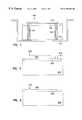
- FIG. 1is an elevational view of an embodiment of a semiconductor wafer having high aspect ratio vias and disposed on a chip carrier according to the teachings of the present invention.
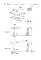
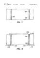
- FIGS. 2, 3 , 4 , 5 , 6 , 7 and 8are elevational views of a semiconductor wafer at various points of an illustrative embodiment of a method for forming an integrated circuit with high aspect ratio vias according to the teachings of the present invention.
- wafer and substrateare interchangeably used to refer generally to any structure on which integrated circuits are formed, and also to such structures during various stages of integrated circuit fabrication. Both terms include doped and undoped semiconductors, epitaxial layers of a semiconductor on a supporting semiconductor or insulating material, combinations of such layers, as well as other such structures that are known in the art.
- horizontalas used in this application is defined as a plane parallel to the conventional plane or surface of a wafer or substrate, regardless of the orientation of the wafer or substrate.
- verticalrefers to a direction perpendicular to the horizonal as defined above. Prepositions, such as “on”, “side” (as in “sidewall”), “higher”, “lower”, “over” and “under” are defined with respect to the conventional plane or surface being on the top surface of the wafer or substrate, regardless of the orientation of the wafer or substrate.
- FIG. 1is an elevational view of an embodiment of the present invention.
- the embodimentincludes semiconductor wafer 100 .
- Semiconductor wafer 100includes high aspect ratio vias 102 that provide low resistance, low inductance connections to leads 104 in chip carrier 106 .
- High aspect ratio vias 102have an aspect ratio in the range of approximately 100 to 200.
- a semiconductor wafer used to form an integrated circuithas a thickness in the range of approximately 500 to 1000 microns.
- the high aspect ratio viascan be fabricated with a width that is in the range from approximately 2.5 microns up to as much as approximately 10 microns.
- Leads 104may be coupled to provide, for example, a ground bus, a guard bus, a power supply bus, clock signals, or other appropriate signals to functional circuit 108 in semiconductor wafer 100 .
- High aspect ratio vias 102advantageously reduce the effect of problems such as ground bounce, substrate bounce, switching noise and power supply noise by providing low impedance and low inductance connections as compared with the much longer, arcing conventional bond wires.
- High aspect ratio vias 102are also coupled to functional circuit 108 through metallization layer 110 .
- High aspect ratio vias 102allow a wide range of functional circuits to be fabricated on wafer 100 .
- high aspect ratio vias 102improve the operation of mixed mode circuits.
- Mixed-mode circuitsinclude analog and digital circuitry that are formed on the same wafer or substrate.
- the switching noise caused by the digital circuitscan interfere with the operation of the analog circuits.
- high aspect ratio vias 102By incorporating high aspect ratio vias 102 , the effect of the switching noise from the digital portion of the functional circuit on the power distribution systems can be reduced.
- high aspect ratio vias 102also satisfy the need for low resistance, low inductance connections to power supply, ground, clock, and guard ring busses in other circuits.
- High aspect ratio vias 102can be added to circuits using a conventional layout for the circuit without adversely affecting the surface area requirements of the circuit.
- Conventional circuitstypically include pads formed on the top surface of the semiconductor wafer that are used to connect to, for example, ground and power supply busses through bond wires.
- the bond wires of conventional circuitscan be replaced by high aspect ratio vias 102 to achieve the advantages described above.
- FIGS. 2, 3 , 4 , 5 , 6 , 7 and 8are elevational views of semiconductor wafer 200 at various points of an illustrative embodiment of a method for forming an integrated circuit with high aspect ratio vias according to the teachings of the present invention.
- Functional circuit 202is formed in an active region of semiconductor wafer 200 .
- semiconductor wafer 200comprises a monocrystalline silicon wafer.
- the Figuresonly show the formation of two high aspect ratio vias through semiconductor wafer 200 .
- any appropriate number of viascan be formed to couple to a selected lead.
- the number of vias needed for a conventional dynamic random access memory (DRAM)may be on the order of 100.
- DRAMdynamic random access memory
- the viasare formed in the same space on the surface of semiconductor wafer 200 that is conventionally used to form bond pads to be connected to the same leads.
- the viasreplace the conventional bond wires which couple the bond pads to the selected leads of a lead frame in the packaging of the semiconductor wafer.
- photo resist layer 204is formed on surface 206 of semiconductor substrate 200 .
- Photo resist layer 204is patterned to provide openings 208 at points on surface 206 where high aspect ratio holes are to be formed through semiconductor wafer 200 .
- etch pits 210are formed by conventional alkaline etching through openings 208 in photo resist layer 204 . Photo resist layer 204 is then removed.
- FIG. 4is a schematic diagram that illustrates an embodiment of a layout of equipment used to carry out an anodic etch that is used to form high aspect ratio holes 250 of FIG. 5 .
- holes 250have an aspect ratio in the range of 100 to 200.
- Bottom surface 262 of semiconductor wafer 200is coupled to voltage source 234 by positive electrode 230 .
- negative electrode 232is coupled to voltage source 234 and is placed in a bath of 6% aqueous solution of hydrofluoric acid (HF) on surface 206 of semiconductor wafer 200 .
- HFhydrofluoric acid
- illumination equipment 236is also included because semiconductor wafer 200 is n-type semiconductor material. When p-type semiconductor material is used, the illumination equipment is not required. Illumination equipment 236 assures that there is a sufficient concentration of holes in semiconductor wafer 200 as required by the anodic etching process. Illumination equipment 236 includes lamp 238 , IR filter 240 , and lens 242 . Illumination equipment 236 focuses light on surface 262 of semiconductor wafer 200 .
- the anodic etchetches high aspect ratio holes through semiconductor wafer 200 at the location of etch pits 210 .
- Voltage source 234is turned on and provides a voltage across positive and negative electrodes 230 and 232 .
- Etching currentflows from positive electrode 230 to surface 206 .
- This currentforms the high aspect ratio holes through semiconductor wafer 200 .
- illumination equipmentilluminates surface 262 of semiconductor wafer 200 so as to assure a sufficient concentration of holes for the anodic etching process.
- the size and shape of the high aspect ratio holes through semiconductor wafer 200depends on, for example, the anodization parameters such as HF concentration, current density, and light illumination.
- An anodic etching processis described in V. Lehmann, The Physics of Macropore Formation in Low Doped-Type Silicon, J. Electrochem. Soc., Vol. 140, No. 10, pp. 2836-2843, October 1993, which is incorporated herein by reference.
- FIG. 5illustrates that electrical insulation can be formed on inner surface 252 of holes 250 .
- simple oxidationon the order of one micron or less is used to form insulator layer 254 on inner surface 252 or holes 250 to provide the electrical insulation.
- FIGS. 6 and 7illustrate a process of aluminum/polysilicon substitution that is used to fill holes 250 with aluminum.
- a process of aluminum/polysilicon substitutionis described in H. Horie et al., Novel High Aspect Ratio Aluminum Plug for Logic/DRAM LSIs Using Polysilicon-Aluminum Substitute, Dig. IEEE Int. Electron Device Meeting, San Francisco, pp. 946-948, 1996, which is incorporated herein by reference.
- hole 250is filled with a layer of polysilicon 256 by a process of chemical vapor deposition (CVD). It is noted that, conventionally, such a deep trench cannot be filled directly with aluminum using a direct chemical vapor deposition technique.
- CVDchemical vapor deposition
- polysiliconhas been deposited in holes with such high aspect ratios, e.g., deep trenches for trench capacitors.
- excess polysilicon on surface 206is removed by, for example, chemical/mechanical polishing.
- Aluminum layers 258 and 260are deposited on surfaces 206 and 262 using, for example, a sputtering technique used to coat optical disks. Layers 258 and 260 have a thickness on the order of a few microns.
- the structure shown in FIG. 6is then annealed at 500 degrees Celsius in Nitrogen ambient. This allows the aluminum material of layers 258 and 260 to be substituted for the polysilicon in holes 250 .
- the displaced polysilicon and any residual aluminum from layers 258 and 260are removed by, for example, chemical/mechanical polishing.
- a thin, e.g, 0.1 ⁇ m, of titaniumon top of layers 258 and 260 the above mentioned anneal can be reduced from 500° Celsius to 450° Celsius.
- the structureis now as shown in FIG. 7 with high aspect ratio vias 264 extending through semiconductor wafer 200 .
- pads 266are formed, using conventional techniques on both first and second surfaces 206 and 262 , respectively, of semiconductor wafer 200 .
- the padsare used to connect a via to metallization layer 268 .
- the bond padsare used to connect a via to a lead 270 .
- a voltage on lead 270can be passed through via 264 to functional circuit 202 without problems such as ground bounce, substrate bounce, and power supply noise, and simultaneous switching noise that can be introduced using conventional bond wires.
- pads 266can be omitted and metallization layer 268 can be brought into contact with an end of a via.
- the high aspect ratio viascan be applied in a wide variety of circuits including but not limited to dynamic random access memory devices, dynamic logic circuits, and other multi-mode circuits. Further, other techniques can be used to form and fill the high aspect ratio holes to form the vias.
Landscapes
- Physics & Mathematics (AREA)
- Condensed Matter Physics & Semiconductors (AREA)
- General Physics & Mathematics (AREA)
- Engineering & Computer Science (AREA)
- Computer Hardware Design (AREA)
- Microelectronics & Electronic Packaging (AREA)
- Power Engineering (AREA)
- Internal Circuitry In Semiconductor Integrated Circuit Devices (AREA)
- Semiconductor Integrated Circuits (AREA)
Abstract
Description
Claims (26)
Priority Applications (2)
| Application Number | Priority Date | Filing Date | Title |
|---|---|---|---|
| US09/009,791US6198168B1 (en) | 1998-01-20 | 1998-01-20 | Integrated circuits using high aspect ratio vias through a semiconductor wafer and method for forming same |
| US09/800,373US6709978B2 (en) | 1998-01-20 | 2001-03-06 | Method for forming integrated circuits using high aspect ratio vias through a semiconductor wafer |
Applications Claiming Priority (1)
| Application Number | Priority Date | Filing Date | Title |
|---|---|---|---|
| US09/009,791US6198168B1 (en) | 1998-01-20 | 1998-01-20 | Integrated circuits using high aspect ratio vias through a semiconductor wafer and method for forming same |
Related Child Applications (1)
| Application Number | Title | Priority Date | Filing Date |
|---|---|---|---|
| US09/800,373DivisionUS6709978B2 (en) | 1998-01-20 | 2001-03-06 | Method for forming integrated circuits using high aspect ratio vias through a semiconductor wafer |
Publications (1)
| Publication Number | Publication Date |
|---|---|
| US6198168B1true US6198168B1 (en) | 2001-03-06 |
Family
ID=21739730
Family Applications (2)
| Application Number | Title | Priority Date | Filing Date |
|---|---|---|---|
| US09/009,791Expired - LifetimeUS6198168B1 (en) | 1998-01-20 | 1998-01-20 | Integrated circuits using high aspect ratio vias through a semiconductor wafer and method for forming same |
| US09/800,373Expired - LifetimeUS6709978B2 (en) | 1998-01-20 | 2001-03-06 | Method for forming integrated circuits using high aspect ratio vias through a semiconductor wafer |
Family Applications After (1)
| Application Number | Title | Priority Date | Filing Date |
|---|---|---|---|
| US09/800,373Expired - LifetimeUS6709978B2 (en) | 1998-01-20 | 2001-03-06 | Method for forming integrated circuits using high aspect ratio vias through a semiconductor wafer |
Country Status (1)
| Country | Link |
|---|---|
| US (2) | US6198168B1 (en) |
Cited By (40)
| Publication number | Priority date | Publication date | Assignee | Title |
|---|---|---|---|---|
| US6452117B2 (en)* | 1999-08-26 | 2002-09-17 | International Business Machines Corporation | Method for filling high aspect ratio via holes in electronic substrates and the resulting holes |
| US20020155655A1 (en)* | 2001-04-18 | 2002-10-24 | Pon Harry Q. | EMI and noise shielding for multi-metal layer high frequency integrated circuit processes |
| US6526191B1 (en)* | 1998-02-26 | 2003-02-25 | Micron Technology, Inc. | Integrated circuits using optical fiber interconnects formed through a semiconductor wafer and methods for forming same |
| US20030045078A1 (en)* | 2001-08-30 | 2003-03-06 | Micron Technology, Inc. | Highly reliable amorphous high-K gate oxide ZrO2 |
| DE10204403A1 (en)* | 2002-02-04 | 2003-08-21 | Infineon Technologies Ag | Device for connecting an IC connection to a reference potential |
| US20030197186A1 (en)* | 1998-02-26 | 2003-10-23 | Micron Technology, Inc. | Integrated circuits using optical waveguide interconnects formed through a semiconductor wafer and methods for forming same |
| US20030207566A1 (en)* | 2001-02-08 | 2003-11-06 | Leonard Forbes | High performance silicon contact for flip chip |
| US20040038195A1 (en)* | 2000-09-20 | 2004-02-26 | Molecular Reflections | Microresonant sensors and methods of use thereof |
| US20040043607A1 (en)* | 2002-08-29 | 2004-03-04 | Farnworth Warren M. | Methods for creating electrophoretically insulated vias in semiconductive substrates and resulting structures |
| US6709978B2 (en) | 1998-01-20 | 2004-03-23 | Micron Technology, Inc. | Method for forming integrated circuits using high aspect ratio vias through a semiconductor wafer |
| US6838310B1 (en)* | 1999-05-03 | 2005-01-04 | United Microelectronics Corporation | Integrated circuit with improved interconnect structure and process for making same |
| US20050026349A1 (en)* | 2001-08-30 | 2005-02-03 | Micron Technology, Inc. | Flash memory with low tunnel barrier interpoly insulators |
| US20050046034A1 (en)* | 2003-09-03 | 2005-03-03 | Micron Technology, Inc. | Apparatus and method for high density multi-chip structures |
| US20050212078A1 (en)* | 2004-03-24 | 2005-09-29 | Youngwoo Kwon | Integrated circuit module package and assembly method thereof |
| US20050277288A1 (en)* | 1997-11-11 | 2005-12-15 | Volkan Ozguz | Stackable semiconductor chip layer comprising prefabricated trench interconnect vias |
| US20060046522A1 (en)* | 2004-08-31 | 2006-03-02 | Micron Technology, Inc. | Atomic layer deposited lanthanum aluminum oxide dielectric layer |
| US20060046505A1 (en)* | 2004-08-26 | 2006-03-02 | Micron Technology, Inc. | Ruthenium gate for a lanthanide oxide dielectric layer |
| US20060097388A1 (en)* | 2002-07-02 | 2006-05-11 | Klaus Breitschwerdt | Electrical system, especially a microelectronic or microelectromechanical high frequency system |
| US20060125030A1 (en)* | 2004-12-13 | 2006-06-15 | Micron Technology, Inc. | Hybrid ALD-CVD of PrxOy/ZrO2 films as gate dielectrics |
| US20060177975A1 (en)* | 2005-02-10 | 2006-08-10 | Micron Technology, Inc. | Atomic layer deposition of CeO2/Al2O3 films as gate dielectrics |
| US7145121B1 (en) | 2000-08-11 | 2006-12-05 | Cook Jr Koy B | Monolithic silicon integrated circuit for detecting azimuth and elevation of incident radiation and method for using same |
| US7179740B1 (en) | 1999-05-03 | 2007-02-20 | United Microelectronics Corporation | Integrated circuit with improved interconnect structure and process for making same |
| US20070049054A1 (en)* | 2005-08-31 | 2007-03-01 | Micron Technology, Inc. | Cobalt titanium oxide dielectric films |
| US20070048926A1 (en)* | 2005-08-31 | 2007-03-01 | Micron Technology, Inc. | Lanthanum aluminum oxynitride dielectric films |
| US20070063202A1 (en)* | 2001-08-24 | 2007-03-22 | Jurgen Leib | Method for producing electronic components |
| US20070071461A1 (en)* | 2005-09-21 | 2007-03-29 | Oki Data Corporation | Printing apparatus |
| US7199050B2 (en) | 2004-08-24 | 2007-04-03 | Micron Technology, Inc. | Pass through via technology for use during the manufacture of a semiconductor device |
| US7405454B2 (en) | 2003-03-04 | 2008-07-29 | Micron Technology, Inc. | Electronic apparatus with deposited dielectric layers |
| US7560793B2 (en) | 2002-05-02 | 2009-07-14 | Micron Technology, Inc. | Atomic layer deposition and conversion |
| US7662729B2 (en) | 2005-04-28 | 2010-02-16 | Micron Technology, Inc. | Atomic layer deposition of a ruthenium layer to a lanthanide oxide dielectric layer |
| US7670646B2 (en) | 2002-05-02 | 2010-03-02 | Micron Technology, Inc. | Methods for atomic-layer deposition |
| US7709402B2 (en) | 2006-02-16 | 2010-05-04 | Micron Technology, Inc. | Conductive layers for hafnium silicon oxynitride films |
| US7728626B2 (en) | 2002-07-08 | 2010-06-01 | Micron Technology, Inc. | Memory utilizing oxide nanolaminates |
| US20100276748A1 (en)* | 2007-06-28 | 2010-11-04 | Ahn Kie Y | Method of forming lutetium and lanthanum dielectric structures |
| US7936059B1 (en)* | 2007-02-20 | 2011-05-03 | Altera Corporation | Lead frame packaging technique with reduced noise and cross-talk |
| US20110248263A1 (en)* | 2010-04-07 | 2011-10-13 | Globalfoundries Inc. | Integrated circuits having backside test structures and methods for the fabrication thereof |
| EP2044626A4 (en)* | 2006-06-29 | 2012-03-14 | Intel Corp | SILICON LEVEL SOLUTION FOR MITIGATION OF SUBSTRATE NOISE |
| US8501563B2 (en) | 2005-07-20 | 2013-08-06 | Micron Technology, Inc. | Devices with nanocrystals and methods of formation |
| US20140305688A1 (en)* | 2013-04-15 | 2014-10-16 | Canon Kabushiki Kaisha | Printed wiring board and printed circuit board |
| US12341099B2 (en) | 2022-09-23 | 2025-06-24 | International Business Machines Corporation | Semiconductor backside transistor integration with backside power delivery network |
Families Citing this family (31)
| Publication number | Priority date | Publication date | Assignee | Title |
|---|---|---|---|---|
| US6831301B2 (en)* | 2001-10-15 | 2004-12-14 | Micron Technology, Inc. | Method and system for electrically coupling a chip to chip package |
| US7221017B2 (en)* | 2002-07-08 | 2007-05-22 | Micron Technology, Inc. | Memory utilizing oxide-conductor nanolaminates |
| US7102855B2 (en)* | 2003-08-15 | 2006-09-05 | Seagate Technology Llc | Microelectronic device with closely spaced contact studs |
| US7067385B2 (en)* | 2003-09-04 | 2006-06-27 | Micron Technology, Inc. | Support for vertically oriented capacitors during the formation of a semiconductor device |
| US7125781B2 (en)* | 2003-09-04 | 2006-10-24 | Micron Technology, Inc. | Methods of forming capacitor devices |
| US6887785B1 (en) | 2004-05-13 | 2005-05-03 | International Business Machines Corporation | Etching openings of different depths using a single mask layer method and structure |
| US7387939B2 (en)* | 2004-07-19 | 2008-06-17 | Micron Technology, Inc. | Methods of forming semiconductor structures and capacitor devices |
| US7439152B2 (en)* | 2004-08-27 | 2008-10-21 | Micron Technology, Inc. | Methods of forming a plurality of capacitors |
| US7202127B2 (en) | 2004-08-27 | 2007-04-10 | Micron Technology, Inc. | Methods of forming a plurality of capacitors |
| US20060046055A1 (en)* | 2004-08-30 | 2006-03-02 | Nan Ya Plastics Corporation | Superfine fiber containing grey dope dyed component and the fabric made of the same |
| US7101789B2 (en)* | 2004-09-13 | 2006-09-05 | General Electric Company | Method of wet etching vias and articles formed thereby |
| US7320911B2 (en)* | 2004-12-06 | 2008-01-22 | Micron Technology, Inc. | Methods of forming pluralities of capacitors |
| US7557015B2 (en)* | 2005-03-18 | 2009-07-07 | Micron Technology, Inc. | Methods of forming pluralities of capacitors |
| EP1722466A1 (en)* | 2005-05-13 | 2006-11-15 | STMicroelectronics S.r.l. | Method and relative circuit for generating a control voltage of a synchronous rectifier |
| US7544563B2 (en)* | 2005-05-18 | 2009-06-09 | Micron Technology, Inc. | Methods of forming a plurality of capacitors |
| US7517753B2 (en)* | 2005-05-18 | 2009-04-14 | Micron Technology, Inc. | Methods of forming pluralities of capacitors |
| US7199005B2 (en)* | 2005-08-02 | 2007-04-03 | Micron Technology, Inc. | Methods of forming pluralities of capacitors |
| US7557013B2 (en)* | 2006-04-10 | 2009-07-07 | Micron Technology, Inc. | Methods of forming a plurality of capacitors |
| US7902081B2 (en)* | 2006-10-11 | 2011-03-08 | Micron Technology, Inc. | Methods of etching polysilicon and methods of forming pluralities of capacitors |
| US7785962B2 (en)* | 2007-02-26 | 2010-08-31 | Micron Technology, Inc. | Methods of forming a plurality of capacitors |
| US7923373B2 (en) | 2007-06-04 | 2011-04-12 | Micron Technology, Inc. | Pitch multiplication using self-assembling materials |
| US7682924B2 (en) | 2007-08-13 | 2010-03-23 | Micron Technology, Inc. | Methods of forming a plurality of capacitors |
| US8388851B2 (en) | 2008-01-08 | 2013-03-05 | Micron Technology, Inc. | Capacitor forming methods |
| US8274777B2 (en) | 2008-04-08 | 2012-09-25 | Micron Technology, Inc. | High aspect ratio openings |
| KR101052870B1 (en) | 2008-04-21 | 2011-07-29 | 주식회사 하이닉스반도체 | A laminated semiconductor package having a through electrode, a circuit board having the same, a semiconductor package having the same, and a semiconductor package |
| US7759193B2 (en)* | 2008-07-09 | 2010-07-20 | Micron Technology, Inc. | Methods of forming a plurality of capacitors |
| US8518788B2 (en) | 2010-08-11 | 2013-08-27 | Micron Technology, Inc. | Methods of forming a plurality of capacitors |
| US9076680B2 (en) | 2011-10-18 | 2015-07-07 | Micron Technology, Inc. | Integrated circuitry, methods of forming capacitors, and methods of forming integrated circuitry comprising an array of capacitors and circuitry peripheral to the array |
| US8946043B2 (en) | 2011-12-21 | 2015-02-03 | Micron Technology, Inc. | Methods of forming capacitors |
| TW201349470A (en)* | 2012-05-16 | 2013-12-01 | Azurewave Technologies Inc | Image sensing module for reducing overall thickness |
| US8652926B1 (en) | 2012-07-26 | 2014-02-18 | Micron Technology, Inc. | Methods of forming capacitors |
Citations (22)
| Publication number | Priority date | Publication date | Assignee | Title |
|---|---|---|---|---|
| US3968564A (en) | 1975-04-30 | 1976-07-13 | Northern Electric Company Limited | Alignment of optical fibers to light emitting diodes |
| US4920070A (en)* | 1987-02-19 | 1990-04-24 | Fujitsu Limited | Method for forming wirings for a semiconductor device by filling very narrow via holes |
| US4970578A (en)* | 1987-05-01 | 1990-11-13 | Raytheon Company | Selective backside plating of GaAs monolithic microwave integrated circuits |
| JPH0313907A (en) | 1989-06-13 | 1991-01-22 | Fujikura Ltd | Production of substrate type optical waveguide |
| WO1991011833A1 (en)* | 1990-01-26 | 1991-08-08 | Commtech International | Chip interconnect with high density of vias |
| US5128831A (en) | 1991-10-31 | 1992-07-07 | Micron Technology, Inc. | High-density electronic package comprising stacked sub-modules which are electrically interconnected by solder-filled vias |
| JPH04263462A (en)* | 1991-02-18 | 1992-09-18 | Fujitsu Ltd | Semiconductor device and manufacture thereof |
| JPH05145060A (en)* | 1991-11-22 | 1993-06-11 | Nec Corp | Structure of semiconductor contact hole and manufacture thereof |
| WO1994005039A1 (en)* | 1992-08-20 | 1994-03-03 | Capps David A | Semiconductor wafer for lamination applications |
| US5352998A (en)* | 1992-10-09 | 1994-10-04 | Mitsubishi Denki Kabushiki Kaisha | Microwave integrated circuit having a passive circuit substrate mounted on a semiconductor circuit substrate |
| US5409563A (en) | 1993-02-26 | 1995-04-25 | Micron Technology, Inc. | Method for etching high aspect ratio features |
| US5532506A (en)* | 1994-08-31 | 1996-07-02 | Texas Instruments Incorporated | Integrated circuit adapted for improved thermal impedance |
| US5604835A (en) | 1993-12-27 | 1997-02-18 | Hitachi, Ltd. | Integrated optical waveguide device |
| US5641545A (en) | 1995-06-07 | 1997-06-24 | Micron Technology, Inc. | Method to deposit highly conformal CVD films |
| US5682062A (en)* | 1995-06-05 | 1997-10-28 | Harris Corporation | System for interconnecting stacked integrated circuits |
| US5742100A (en)* | 1995-03-27 | 1998-04-21 | Motorola, Inc. | Structure having flip-chip connected substrates |
| US5834849A (en)* | 1996-02-13 | 1998-11-10 | Altera Corporation | High density integrated circuit pad structures |
| US5844289A (en) | 1996-05-21 | 1998-12-01 | Nec Corporation | Solid-state image sensor with microlens and optical fiber bundle |
| US5901050A (en)* | 1996-08-21 | 1999-05-04 | Ngk Spark Plug Co., Ltd. | Wired base plate and package for electronic parts |
| US5900674A (en)* | 1996-12-23 | 1999-05-04 | General Electric Company | Interface structures for electronic devices |
| US5903045A (en)* | 1996-04-30 | 1999-05-11 | International Business Machines Corporation | Self-aligned connector for stacked chip module |
| US5952665A (en) | 1997-11-28 | 1999-09-14 | Nanocrystals Technology L.P. | Composite nanophosphor screen for detecting radiation |
Family Cites Families (31)
| Publication number | Priority date | Publication date | Assignee | Title |
|---|---|---|---|---|
| JPS565567A (en)* | 1979-06-27 | 1981-01-21 | Canon Inc | Image forming method |
| JPS61258468A (en)* | 1985-05-13 | 1986-11-15 | Hitachi Ltd | Semiconductor memory device and manufacture of the same |
| US4744623A (en) | 1985-10-16 | 1988-05-17 | The Trustees Of Columbia University In The City Of New York | Integrated fiber optic coupler for VHSIC/VLSI interconnects |
| US5312765A (en) | 1991-06-28 | 1994-05-17 | Hughes Aircraft Company | Method of fabricating three dimensional gallium arsenide microelectronic device |
| US5221633A (en) | 1991-09-09 | 1993-06-22 | Motorola, Inc. | Method of manufacturing a distributed drive optoelectronic integrated circuit |
| JP2692461B2 (en) | 1991-10-26 | 1997-12-17 | 日本電気株式会社 | Semiconductor device |
| US5489554A (en) | 1992-07-21 | 1996-02-06 | Hughes Aircraft Company | Method of making a 3-dimensional circuit assembly having electrical contacts that extend through the IC layer |
| US5651855A (en)* | 1992-07-28 | 1997-07-29 | Micron Technology, Inc. | Method of making self aligned contacts to silicon substrates during the manufacture of integrated circuits |
| DE4314906C2 (en) | 1993-05-05 | 1996-10-31 | Siemens Ag | Semiconductor component with power connections for high integration density |
| DE4314907C1 (en) | 1993-05-05 | 1994-08-25 | Siemens Ag | Method for producing semiconductor components making electrically conducting contact with one another vertically |
| US5416872A (en) | 1993-07-06 | 1995-05-16 | At&T Corp. | Arrangement for interconnecting an optical fiber an optoelectronic component |
| EP0721662A1 (en) | 1993-09-30 | 1996-07-17 | Kopin Corporation | Three-dimensional processor using transferred thin film circuits |
| US5729038A (en) | 1995-12-15 | 1998-03-17 | Harris Corporation | Silicon-glass bonded wafers |
| US5902118A (en) | 1994-07-05 | 1999-05-11 | Siemens Aktiengesellschaft | Method for production of a three-dimensional circuit arrangement |
| US5587119A (en)* | 1994-09-14 | 1996-12-24 | E-Systems, Inc. | Method for manufacturing a coaxial interconnect |
| US5796714A (en) | 1994-09-28 | 1998-08-18 | Matsushita Electric Industrial Co., Ltd. | Optical module having a vertical-cavity surface-emitting laser |
| US5618752A (en) | 1995-06-05 | 1997-04-08 | Harris Corporation | Method of fabrication of surface mountable integrated circuits |
| US5739067A (en) | 1995-12-07 | 1998-04-14 | Advanced Micro Devices, Inc. | Method for forming active devices on and in exposed surfaces of both sides of a silicon wafer |
| US5858814A (en) | 1996-07-17 | 1999-01-12 | Lucent Technologies Inc. | Hybrid chip and method therefor |
| JPH1051247A (en)* | 1996-07-29 | 1998-02-20 | Toshiba Corp | Fully differential analog circuit |
| US5760478A (en) | 1996-08-20 | 1998-06-02 | International Business Machines Corporation | Clock skew minimization system and method for integrated circuits |
| US5897333A (en) | 1997-03-14 | 1999-04-27 | Lucent Technologies, Inc. | Method for forming integrated composite semiconductor devices |
| US5915167A (en) | 1997-04-04 | 1999-06-22 | Elm Technology Corporation | Three dimensional structure memory |
| KR100248054B1 (en) | 1997-08-14 | 2000-03-15 | 윤종용 | Fiber Array Module Using Soldering and Manufacturing Method |
| US6187677B1 (en)* | 1997-08-22 | 2001-02-13 | Micron Technology, Inc. | Integrated circuitry and methods of forming integrated circuitry |
| US6143616A (en)* | 1997-08-22 | 2000-11-07 | Micron Technology, Inc. | Methods of forming coaxial integrated circuitry interconnect lines |
| US6198168B1 (en) | 1998-01-20 | 2001-03-06 | Micron Technologies, Inc. | Integrated circuits using high aspect ratio vias through a semiconductor wafer and method for forming same |
| US6150188A (en) | 1998-02-26 | 2000-11-21 | Micron Technology Inc. | Integrated circuits using optical fiber interconnects formed through a semiconductor wafer and methods for forming same |
| US6090636A (en) | 1998-02-26 | 2000-07-18 | Micron Technology, Inc. | Integrated circuits using optical waveguide interconnects formed through a semiconductor wafer and methods for forming same |
| US6281042B1 (en)* | 1998-08-31 | 2001-08-28 | Micron Technology, Inc. | Structure and method for a high performance electronic packaging assembly |
| US6122187A (en)* | 1998-11-23 | 2000-09-19 | Micron Technology, Inc. | Stacked integrated circuits |
- 1998
- 1998-01-20USUS09/009,791patent/US6198168B1/ennot_activeExpired - Lifetime
- 2001
- 2001-03-06USUS09/800,373patent/US6709978B2/ennot_activeExpired - Lifetime
Patent Citations (22)
| Publication number | Priority date | Publication date | Assignee | Title |
|---|---|---|---|---|
| US3968564A (en) | 1975-04-30 | 1976-07-13 | Northern Electric Company Limited | Alignment of optical fibers to light emitting diodes |
| US4920070A (en)* | 1987-02-19 | 1990-04-24 | Fujitsu Limited | Method for forming wirings for a semiconductor device by filling very narrow via holes |
| US4970578A (en)* | 1987-05-01 | 1990-11-13 | Raytheon Company | Selective backside plating of GaAs monolithic microwave integrated circuits |
| JPH0313907A (en) | 1989-06-13 | 1991-01-22 | Fujikura Ltd | Production of substrate type optical waveguide |
| WO1991011833A1 (en)* | 1990-01-26 | 1991-08-08 | Commtech International | Chip interconnect with high density of vias |
| JPH04263462A (en)* | 1991-02-18 | 1992-09-18 | Fujitsu Ltd | Semiconductor device and manufacture thereof |
| US5128831A (en) | 1991-10-31 | 1992-07-07 | Micron Technology, Inc. | High-density electronic package comprising stacked sub-modules which are electrically interconnected by solder-filled vias |
| JPH05145060A (en)* | 1991-11-22 | 1993-06-11 | Nec Corp | Structure of semiconductor contact hole and manufacture thereof |
| WO1994005039A1 (en)* | 1992-08-20 | 1994-03-03 | Capps David A | Semiconductor wafer for lamination applications |
| US5352998A (en)* | 1992-10-09 | 1994-10-04 | Mitsubishi Denki Kabushiki Kaisha | Microwave integrated circuit having a passive circuit substrate mounted on a semiconductor circuit substrate |
| US5409563A (en) | 1993-02-26 | 1995-04-25 | Micron Technology, Inc. | Method for etching high aspect ratio features |
| US5604835A (en) | 1993-12-27 | 1997-02-18 | Hitachi, Ltd. | Integrated optical waveguide device |
| US5532506A (en)* | 1994-08-31 | 1996-07-02 | Texas Instruments Incorporated | Integrated circuit adapted for improved thermal impedance |
| US5742100A (en)* | 1995-03-27 | 1998-04-21 | Motorola, Inc. | Structure having flip-chip connected substrates |
| US5682062A (en)* | 1995-06-05 | 1997-10-28 | Harris Corporation | System for interconnecting stacked integrated circuits |
| US5641545A (en) | 1995-06-07 | 1997-06-24 | Micron Technology, Inc. | Method to deposit highly conformal CVD films |
| US5834849A (en)* | 1996-02-13 | 1998-11-10 | Altera Corporation | High density integrated circuit pad structures |
| US5903045A (en)* | 1996-04-30 | 1999-05-11 | International Business Machines Corporation | Self-aligned connector for stacked chip module |
| US5844289A (en) | 1996-05-21 | 1998-12-01 | Nec Corporation | Solid-state image sensor with microlens and optical fiber bundle |
| US5901050A (en)* | 1996-08-21 | 1999-05-04 | Ngk Spark Plug Co., Ltd. | Wired base plate and package for electronic parts |
| US5900674A (en)* | 1996-12-23 | 1999-05-04 | General Electric Company | Interface structures for electronic devices |
| US5952665A (en) | 1997-11-28 | 1999-09-14 | Nanocrystals Technology L.P. | Composite nanophosphor screen for detecting radiation |
Non-Patent Citations (21)
| Title |
|---|
| Forbes, L., et al., "Resonant Forward-Biased Guard-Ring Diodes for Suppression of Substrate Noise in Mixed-Mode CMOS Circuits", Electronics Letters, 31, 720-721, (Apr. 1995). |
| Foster, R., et al., "High Rate Low-Temperature Selective Tungsten", In: Tungsten and Other Refactory Metals for VLSI Applications III, V.A. Wells, ed., Materials Res. Soc., Pittsburg, PA, 69-72, (1988). |
| Gong, S., et al., "Techniques for Redaing Switching Noise in High Speed Digital Systems", Proceedings of the 8th Annual IEEE International ASIC Conference and Exhibit, 21-24, (1995). |
| Heavens, O., Optical Properties of Thin Solid Films, Dover Pubs. Inc., New York, 167, (1965). |
| Horie, H., et al., "Novel High Aspect Ratio Aluminium Plug for Logic/DRAM LSI's Using Polysillicon-Aluminium Substitute", Technical Digest: IEEE Int. Electron Devices Meeting, San Francisco, CA, 946-948, (1996). |
| Kim, Y.S., et al., "A Study on Pyrolysis DMEAA for Selective Deposition of Aluminium", In: Advanced Metallization and Interconnect Systems for ULSI Applications in 1995, R.C. Ellwanger, et al., (eds.), Materials Research Society, Pittsburg, PA, 675-680, (1996). |
| Klaus, et al., "Atomic Layer Controlled Growth of SiO2 Films Using Binary Reaction Sequence Chemistry", Applied Physics Lett. 70(9), 1092-94, (Mar. 3, 1997). |
| Lehmann, et al., "A Novel Capacitor Technology Based on Porous Silicon", Thin Solid Films 276, Elsevier Science, 138-42, (1996). |
| Lehmann, V., "The Physics of Macropore Formation in Loa Doped n-Type Silicon", J. Electrochem. Soc., 140, 2836-2843, (Oct. 1993). |
| Masu, K. et al., "Multilevel Based Metaalization on AA CVD", 1996 IEEE Symposium, on VLSI Technology, Digest of Technical Papers, Honolulu, HI, 44-45, (Jun. 11-13, 1996). |
| McCredie, B.D., et al., "Modeling, Measurement, and Simulation of Simultaneous Switching Noise", IEEE Transactions on Components, Packaging, and Manufacturing Technoogy-Part B, 19, 461-472, (Aug. 1996). |
| Muller, K., et al., "Trench Storage Node Technology for Gigabit DRAM Generations", Digest IEEE Int. Electron Device Meeting, San Francisco, CA, 594-597, (Dec. 1996). |
| Ohba, T, et al., "Selective Chemical Vapor Deposition of Tungsten Using Silane and Polysilane Reductions", In: Tungsten and Other Refractory Metals for VLSI Applications IV, Materials Research Society, Pittsburgh, PA, 17-25, (1989). |
| Ohba, T., et al., "Evaluation on Selective Deposition of CVD W Films by Measurement of Surface Temperature", In: Tungsten and Other Refractory Metals for VLSI Applications II, Materials Research Society, Pittsburgh, PA, 59-66, (1987). |
| Ott, A.W., et al., "Al303 Thin Film Growth on Si(100) Using Binary Reaction Sequence Chemistry", Thin Solid Films, vol. 292, 135-44, (1997). |
| Senthinathan, R., et al., "Reference Plane Parasitics Modeling and Their Contribution to the Power and Ground Path "Effective" Inductance as Seen by the Output Drivers", IEEE Transactions on Microwave Theory and Techniques, 42, 1765-1773, (Sep. 1994). |
| Stanisic, B.R., et al., "Addressing Noise Decoupling in Mixed-Signal IC's: Power Distributuon Design and Cell Customization", IEEE Journal of Solid-State Circuits, 30, 321-236, (Mar. 1995). |
| Suntola, T., "Atomic Layer Epitaxy", Handbook of Crystal Growth 3, Thin Films of Epitaxy, Part B: Growth Mechanics and Dyamics, Elsevier, Amsterdam, 601-63, (1994). |
| Sze, S.M., VLSI Technology, 2nd Edition, Mc Graw-Hill, NY, 90, (1988).* |
| Vittal, A., et al., "Clock Skew Optimization for Ground Bounce Control", 1996 IEEE/ACM International Conference on Computer-Aided Design, Digest of Technical papers, San Jose, CA, 395-399, (Nov. 10-14, 1996).* |
| Wooley, et al., "Experimental Results and Modeling Techniques for Substrate Noise in Mixed Signal Integrated Circuits", IEEE Journal of Solid State Circuits, vol. SC-28, 420-30, (1993).* |
Cited By (115)
| Publication number | Priority date | Publication date | Assignee | Title |
|---|---|---|---|---|
| US7786562B2 (en)* | 1997-11-11 | 2010-08-31 | Volkan Ozguz | Stackable semiconductor chip layer comprising prefabricated trench interconnect vias |
| US20100291735A1 (en)* | 1997-11-11 | 2010-11-18 | Volkan Ozguz | Stackable semiconductor chip layer comprising prefabricated trench interconnect vias |
| US20050277288A1 (en)* | 1997-11-11 | 2005-12-15 | Volkan Ozguz | Stackable semiconductor chip layer comprising prefabricated trench interconnect vias |
| US6709978B2 (en) | 1998-01-20 | 2004-03-23 | Micron Technology, Inc. | Method for forming integrated circuits using high aspect ratio vias through a semiconductor wafer |
| US7547954B2 (en) | 1998-02-26 | 2009-06-16 | Micron Technology, Inc. | Electronic systems using optical waveguide interconnects formed through a semiconductor wafer |
| US20030197186A1 (en)* | 1998-02-26 | 2003-10-23 | Micron Technology, Inc. | Integrated circuits using optical waveguide interconnects formed through a semiconductor wafer and methods for forming same |
| US20060131684A1 (en)* | 1998-02-26 | 2006-06-22 | Micron Technology, Inc. | Integrated circuits using optical waveguide interconnects formed through a semiconductor wafer and methods for forming same |
| US20070114543A1 (en)* | 1998-02-26 | 2007-05-24 | Micron Technology, Inc. | Electronic systems using optical waveguide interconnects formed through a semiconductor wafer |
| US6995443B2 (en) | 1998-02-26 | 2006-02-07 | Micron Technology, Inc. | Integrated circuits using optical fiber interconnects formed through a semiconductor wafer |
| US7164156B2 (en) | 1998-02-26 | 2007-01-16 | Micron Technology, Inc. | Electronic systems using optical waveguide interconnects formed throught a semiconductor wafer |
| US6526191B1 (en)* | 1998-02-26 | 2003-02-25 | Micron Technology, Inc. | Integrated circuits using optical fiber interconnects formed through a semiconductor wafer and methods for forming same |
| US6723577B1 (en) | 1998-02-26 | 2004-04-20 | Micron Technology, Inc. | Method of forming an optical fiber interconnect through a semiconductor wafer |
| US6995441B2 (en)* | 1998-02-26 | 2006-02-07 | Micron Technology, Inc. | Integrated circuits using optical waveguide interconnects formed through a semiconductor wafer and methods for forming same |
| US20040156578A1 (en)* | 1998-02-26 | 2004-08-12 | Micron Technology, Inc. | Integrated circuits using optical fiber interconnects formed through a semiconductor wafer |
| US6777715B1 (en)* | 1998-02-26 | 2004-08-17 | Micron Technology, Inc. | Integrated circuits using optical waveguide interconnects formed through a semiconductor wafer and methods for forming same |
| US7179740B1 (en) | 1999-05-03 | 2007-02-20 | United Microelectronics Corporation | Integrated circuit with improved interconnect structure and process for making same |
| US6838310B1 (en)* | 1999-05-03 | 2005-01-04 | United Microelectronics Corporation | Integrated circuit with improved interconnect structure and process for making same |
| US6452117B2 (en)* | 1999-08-26 | 2002-09-17 | International Business Machines Corporation | Method for filling high aspect ratio via holes in electronic substrates and the resulting holes |
| US7145121B1 (en) | 2000-08-11 | 2006-12-05 | Cook Jr Koy B | Monolithic silicon integrated circuit for detecting azimuth and elevation of incident radiation and method for using same |
| US7814652B2 (en) | 2000-09-20 | 2010-10-19 | Bioscale, Inc. | Method of making through-hole vias in a substrate |
| US20090074951A1 (en)* | 2000-09-20 | 2009-03-19 | Bioscale, Inc. | Substrates having through-hole vias and method of making same |
| US20050040907A1 (en)* | 2000-09-20 | 2005-02-24 | Molecular Reflections | System and method for processing capacitive signals |
| US20040038195A1 (en)* | 2000-09-20 | 2004-02-26 | Molecular Reflections | Microresonant sensors and methods of use thereof |
| US20040043423A1 (en)* | 2000-09-20 | 2004-03-04 | Molecular Reflections | Substrates having through-hole vias and method of making same |
| US20030207566A1 (en)* | 2001-02-08 | 2003-11-06 | Leonard Forbes | High performance silicon contact for flip chip |
| US6828656B2 (en) | 2001-02-08 | 2004-12-07 | Micron Technology, Inc. | High performance silicon contact for flip chip and a system using same |
| US6812137B2 (en) | 2001-02-08 | 2004-11-02 | Micron Technology, Inc. | Method of forming coaxial integrated circuitry interconnect lines |
| US6737740B2 (en) | 2001-02-08 | 2004-05-18 | Micron Technology, Inc. | High performance silicon contact for flip chip |
| US20020155655A1 (en)* | 2001-04-18 | 2002-10-24 | Pon Harry Q. | EMI and noise shielding for multi-metal layer high frequency integrated circuit processes |
| US6800918B2 (en)* | 2001-04-18 | 2004-10-05 | Intel Corporation | EMI and noise shielding for multi-metal layer high frequency integrated circuit processes |
| US8114304B2 (en) | 2001-08-24 | 2012-02-14 | Wafer-Level Packaging Portfolio Llc | Method for producing electronic components |
| US20070063202A1 (en)* | 2001-08-24 | 2007-03-22 | Jurgen Leib | Method for producing electronic components |
| SG161099A1 (en)* | 2001-08-24 | 2010-05-27 | Schott Ag | Method for producing electronic components |
| US8026161B2 (en) | 2001-08-30 | 2011-09-27 | Micron Technology, Inc. | Highly reliable amorphous high-K gate oxide ZrO2 |
| US8652957B2 (en) | 2001-08-30 | 2014-02-18 | Micron Technology, Inc. | High-K gate dielectric oxide |
| US20030045078A1 (en)* | 2001-08-30 | 2003-03-06 | Micron Technology, Inc. | Highly reliable amorphous high-K gate oxide ZrO2 |
| US20050026349A1 (en)* | 2001-08-30 | 2005-02-03 | Micron Technology, Inc. | Flash memory with low tunnel barrier interpoly insulators |
| US7259434B2 (en) | 2001-08-30 | 2007-08-21 | Micron Technology, Inc. | Highly reliable amorphous high-k gate oxide ZrO2 |
| US20070048923A1 (en)* | 2001-08-30 | 2007-03-01 | Micron Technology, Inc. | Flash memory with low tunnel barrier interpoly insulators |
| US7545674B2 (en) | 2001-08-30 | 2009-06-09 | Micron Technology, Inc. | Flash memory with low tunnel barrier interpoly insulators |
| US20050029605A1 (en)* | 2001-08-30 | 2005-02-10 | Micron Technology, Inc. | Highly reliable amorphous high-k gate oxide ZrO2 |
| DE10204403A1 (en)* | 2002-02-04 | 2003-08-21 | Infineon Technologies Ag | Device for connecting an IC connection to a reference potential |
| US7057271B2 (en) | 2002-02-04 | 2006-06-06 | Infineon Technologies Ag | Apparatus for connecting an IC terminal to a reference potential |
| US20050067697A1 (en)* | 2002-02-04 | 2005-03-31 | Infineon Technologies Ag | Apparatus for connecting an IC terminal to a reference potential |
| US7670646B2 (en) | 2002-05-02 | 2010-03-02 | Micron Technology, Inc. | Methods for atomic-layer deposition |
| US7560793B2 (en) | 2002-05-02 | 2009-07-14 | Micron Technology, Inc. | Atomic layer deposition and conversion |
| US7589029B2 (en) | 2002-05-02 | 2009-09-15 | Micron Technology, Inc. | Atomic layer deposition and conversion |
| US20060097388A1 (en)* | 2002-07-02 | 2006-05-11 | Klaus Breitschwerdt | Electrical system, especially a microelectronic or microelectromechanical high frequency system |
| US8228725B2 (en) | 2002-07-08 | 2012-07-24 | Micron Technology, Inc. | Memory utilizing oxide nanolaminates |
| US7728626B2 (en) | 2002-07-08 | 2010-06-01 | Micron Technology, Inc. | Memory utilizing oxide nanolaminates |
| US7498670B2 (en) | 2002-08-29 | 2009-03-03 | Micron Technology, Inc. | Semiconductor structures having electrophoretically insulated vias |
| US7105921B2 (en) | 2002-08-29 | 2006-09-12 | Micron Technology, Inc. | Semiconductor assemblies having electrophoretically insulated vias |
| US7105437B2 (en) | 2002-08-29 | 2006-09-12 | Micron Technology, Inc. | Methods for creating electrophoretically insulated vias in semiconductive substrates |
| US7030010B2 (en) | 2002-08-29 | 2006-04-18 | Micron Technology, Inc. | Methods for creating electrophoretically insulated vias in semiconductive substrates and resulting structures |
| US20040043607A1 (en)* | 2002-08-29 | 2004-03-04 | Farnworth Warren M. | Methods for creating electrophoretically insulated vias in semiconductive substrates and resulting structures |
| US20060063377A1 (en)* | 2002-08-29 | 2006-03-23 | Farnworth Warren M | Methods for creating electrophoretically insulated vias in semiconductive substrates |
| US20060027911A1 (en)* | 2002-08-29 | 2006-02-09 | Farnworth Warren M | Methods for creating electrophoretically insulated vias in semiconductive substrates and resulting structures |
| US20070004197A1 (en)* | 2002-08-29 | 2007-01-04 | Farnworth Warren M | Methods for creating electrophoretically insulated vias in semiconductive substrates |
| US7335981B2 (en) | 2002-08-29 | 2008-02-26 | Micron Technology, Inc. | Methods for creating electrophoretically insulated vias in semiconductive substrates |
| US7405454B2 (en) | 2003-03-04 | 2008-07-29 | Micron Technology, Inc. | Electronic apparatus with deposited dielectric layers |
| US20060289990A1 (en)* | 2003-09-03 | 2006-12-28 | Micron Technology, Inc. | Apparatus and method for high density multi-chip structures |
| US20060063302A1 (en)* | 2003-09-03 | 2006-03-23 | Micron Technology, Inc. | Apparatus and method for high density multi-chip structures |
| US7560305B2 (en) | 2003-09-03 | 2009-07-14 | Micron Technology, Inc. | Apparatus and method for high density multi-chip structures |
| US8592964B2 (en) | 2003-09-03 | 2013-11-26 | Micron Technology, Inc. | Apparatus and method for high density multi-chip structures |
| US20050046034A1 (en)* | 2003-09-03 | 2005-03-03 | Micron Technology, Inc. | Apparatus and method for high density multi-chip structures |
| US9209127B2 (en) | 2003-09-03 | 2015-12-08 | Micron Technology | Apparatus and method for high density multi-chip structures |
| US20050212106A1 (en)* | 2004-03-24 | 2005-09-29 | Youngwoo Kwon | Multilayer integrated circuit for RF communication and method for assembly thereof |
| US8067824B2 (en) | 2004-03-24 | 2011-11-29 | Avago Technologies Wireless Ip (Singapore) Pte. Ltd. | Integrated circuit module package and assembly method thereof |
| US20050212078A1 (en)* | 2004-03-24 | 2005-09-29 | Youngwoo Kwon | Integrated circuit module package and assembly method thereof |
| US20070170583A1 (en)* | 2004-03-24 | 2007-07-26 | Youngwoo Kwon | Multilayer integrated circuit for RF communication and method for assembly thereof |
| US7132747B2 (en)* | 2004-03-24 | 2006-11-07 | Youngwoo Kwon | Multilayer integrated circuit for RF communication and method for assembly thereof |
| US7638364B2 (en) | 2004-03-24 | 2009-12-29 | Avago Technologies Wireless Ip (Singapore) Pte. Ltd. | Multilayer integrated circuit for RF communication and method for assembly thereof |
| US7791207B2 (en) | 2004-08-24 | 2010-09-07 | Micron Technology, Inc. | Pass through via technology for use during the manufacture of a semiconductor device |
| US7498260B2 (en) | 2004-08-24 | 2009-03-03 | Micron Technology, Inc. | Pass through via technology for use during the manufacture of a semiconductor device |
| US7199050B2 (en) | 2004-08-24 | 2007-04-03 | Micron Technology, Inc. | Pass through via technology for use during the manufacture of a semiconductor device |
| US20070178694A1 (en)* | 2004-08-24 | 2007-08-02 | Hiatt William M | Pass through via technology for use during the manufacture of a semiconductor device |
| US7081421B2 (en) | 2004-08-26 | 2006-07-25 | Micron Technology, Inc. | Lanthanide oxide dielectric layer |
| US8907486B2 (en) | 2004-08-26 | 2014-12-09 | Micron Technology, Inc. | Ruthenium for a dielectric containing a lanthanide |
| US8558325B2 (en) | 2004-08-26 | 2013-10-15 | Micron Technology, Inc. | Ruthenium for a dielectric containing a lanthanide |
| US7719065B2 (en) | 2004-08-26 | 2010-05-18 | Micron Technology, Inc. | Ruthenium layer for a dielectric layer containing a lanthanide oxide |
| US20060046505A1 (en)* | 2004-08-26 | 2006-03-02 | Micron Technology, Inc. | Ruthenium gate for a lanthanide oxide dielectric layer |
| US7494939B2 (en) | 2004-08-31 | 2009-02-24 | Micron Technology, Inc. | Methods for forming a lanthanum-metal oxide dielectric layer |
| US8237216B2 (en) | 2004-08-31 | 2012-08-07 | Micron Technology, Inc. | Apparatus having a lanthanum-metal oxide semiconductor device |
| US20060046522A1 (en)* | 2004-08-31 | 2006-03-02 | Micron Technology, Inc. | Atomic layer deposited lanthanum aluminum oxide dielectric layer |
| US7867919B2 (en) | 2004-08-31 | 2011-01-11 | Micron Technology, Inc. | Method of fabricating an apparatus having a lanthanum-metal oxide dielectric layer |
| US20060125030A1 (en)* | 2004-12-13 | 2006-06-15 | Micron Technology, Inc. | Hybrid ALD-CVD of PrxOy/ZrO2 films as gate dielectrics |
| US7374964B2 (en) | 2005-02-10 | 2008-05-20 | Micron Technology, Inc. | Atomic layer deposition of CeO2/Al2O3 films as gate dielectrics |
| US20060177975A1 (en)* | 2005-02-10 | 2006-08-10 | Micron Technology, Inc. | Atomic layer deposition of CeO2/Al2O3 films as gate dielectrics |
| US7518246B2 (en) | 2005-02-10 | 2009-04-14 | Micron Technology, Inc. | Atomic layer deposition of CeO2/Al2O3 films as gate dielectrics |
| US7754618B2 (en) | 2005-02-10 | 2010-07-13 | Micron Technology, Inc. | Method of forming an apparatus having a dielectric containing cerium oxide and aluminum oxide |
| US20080248618A1 (en)* | 2005-02-10 | 2008-10-09 | Micron Technology, Inc. | ATOMIC LAYER DEPOSITION OF CeO2/Al2O3 FILMS AS GATE DIELECTRICS |
| US7662729B2 (en) | 2005-04-28 | 2010-02-16 | Micron Technology, Inc. | Atomic layer deposition of a ruthenium layer to a lanthanide oxide dielectric layer |
| US8501563B2 (en) | 2005-07-20 | 2013-08-06 | Micron Technology, Inc. | Devices with nanocrystals and methods of formation |
| US8921914B2 (en) | 2005-07-20 | 2014-12-30 | Micron Technology, Inc. | Devices with nanocrystals and methods of formation |
| US8895442B2 (en) | 2005-08-31 | 2014-11-25 | Micron Technology, Inc. | Cobalt titanium oxide dielectric films |
| US7410910B2 (en) | 2005-08-31 | 2008-08-12 | Micron Technology, Inc. | Lanthanum aluminum oxynitride dielectric films |
| US8071476B2 (en) | 2005-08-31 | 2011-12-06 | Micron Technology, Inc. | Cobalt titanium oxide dielectric films |
| US7531869B2 (en) | 2005-08-31 | 2009-05-12 | Micron Technology, Inc. | Lanthanum aluminum oxynitride dielectric films |
| US20070049054A1 (en)* | 2005-08-31 | 2007-03-01 | Micron Technology, Inc. | Cobalt titanium oxide dielectric films |
| US20070048926A1 (en)* | 2005-08-31 | 2007-03-01 | Micron Technology, Inc. | Lanthanum aluminum oxynitride dielectric films |
| US8455959B2 (en) | 2005-08-31 | 2013-06-04 | Micron Technology, Inc. | Apparatus containing cobalt titanium oxide |
| US20070071461A1 (en)* | 2005-09-21 | 2007-03-29 | Oki Data Corporation | Printing apparatus |
| US7709402B2 (en) | 2006-02-16 | 2010-05-04 | Micron Technology, Inc. | Conductive layers for hafnium silicon oxynitride films |
| US8785312B2 (en) | 2006-02-16 | 2014-07-22 | Micron Technology, Inc. | Conductive layers for hafnium silicon oxynitride |
| US8067794B2 (en) | 2006-02-16 | 2011-11-29 | Micron Technology, Inc. | Conductive layers for hafnium silicon oxynitride films |
| EP2044626A4 (en)* | 2006-06-29 | 2012-03-14 | Intel Corp | SILICON LEVEL SOLUTION FOR MITIGATION OF SUBSTRATE NOISE |
| US7936059B1 (en)* | 2007-02-20 | 2011-05-03 | Altera Corporation | Lead frame packaging technique with reduced noise and cross-talk |
| US8071443B2 (en) | 2007-06-28 | 2011-12-06 | Micron Technology, Inc. | Method of forming lutetium and lanthanum dielectric structures |
| US8847334B2 (en) | 2007-06-28 | 2014-09-30 | Micron Technology, Inc. | Method of forming lutetium and lanthanum dielectric structures |
| US20100276748A1 (en)* | 2007-06-28 | 2010-11-04 | Ahn Kie Y | Method of forming lutetium and lanthanum dielectric structures |
| US8349734B2 (en)* | 2010-04-07 | 2013-01-08 | GlobalFoundries, Inc. | Integrated circuits having backside test structures and methods for the fabrication thereof |
| US20110248263A1 (en)* | 2010-04-07 | 2011-10-13 | Globalfoundries Inc. | Integrated circuits having backside test structures and methods for the fabrication thereof |
| US20140305688A1 (en)* | 2013-04-15 | 2014-10-16 | Canon Kabushiki Kaisha | Printed wiring board and printed circuit board |
| US9560758B2 (en)* | 2013-04-15 | 2017-01-31 | Canon Kabushiki Kaisha | Uniform impedance circuit board |
| US12341099B2 (en) | 2022-09-23 | 2025-06-24 | International Business Machines Corporation | Semiconductor backside transistor integration with backside power delivery network |
Also Published As
| Publication number | Publication date |
|---|---|
| US20020127835A1 (en) | 2002-09-12 |
| US6709978B2 (en) | 2004-03-23 |
Similar Documents
| Publication | Publication Date | Title |
|---|---|---|
| US6198168B1 (en) | Integrated circuits using high aspect ratio vias through a semiconductor wafer and method for forming same | |
| US6395630B2 (en) | Stacked integrated circuits | |
| US6617681B1 (en) | Interposer and method of making same | |
| US5424245A (en) | Method of forming vias through two-sided substrate | |
| US5529950A (en) | Method for manufacturing a cubically integrated circuit arrangement | |
| KR19980081093A (en) | Electrical contact point for buried SOH structure and its manufacturing method | |
| US20030094654A1 (en) | Method and semiconductor structure for implementing buried dual rail power distribution and integrated decoupling capacitance for silicon on insulator (SOI) devices | |
| US5449946A (en) | Semiconductor device provided with isolation region | |
| KR0148679B1 (en) | Stacked insulating film containing yttrium oxide | |
| US5365405A (en) | Multi-chip module | |
| JPS6276653A (en) | semiconductor integrated circuit | |
| US6432724B1 (en) | Buried ground plane for high performance system modules | |
| US5296734A (en) | Semiconductor integrated circuit having silicon nitride provided as insulator of capacitor | |
| JPS59175153A (en) | Semiconductor integrated circuit | |
| KR100466224B1 (en) | Fabrication method of base substrate for mounting semiconductor chip | |
| US20240266289A1 (en) | Semiconductor structure and method of forming semiconductor structure | |
| KR100405194B1 (en) | A fabrication method of selectively oxidized porous silicon(SOPS) layer, a multi-chip package of using the same, and a semiconductor substrate | |
| JPS639964A (en) | Manufacture of semiconductor storage element | |
| US6727578B1 (en) | Semiconductor device having power supply voltage routed through substrate | |
| KR100910006B1 (en) | Capacitor Formation Method for Semiconductor Device | |
| JPS6022343A (en) | Multilayer interconnection structure of semiconductor integrated circuit device | |
| CN117393553A (en) | Semiconductor device including decoupling capacitor and manufacturing method | |
| CN116936466A (en) | Method for forming semiconductor structure | |
| JPS63148675A (en) | semiconductor equipment | |
| JPH0365654B2 (en) |
Legal Events
| Date | Code | Title | Description |
|---|---|---|---|
| AS | Assignment | Owner name:MICRON TECHNOLOGY, INC., IDAHO Free format text:ASSIGNMENT OF ASSIGNORS INTEREST;ASSIGNORS:GEUSIC, JOSEPH E.;AHN, KIE Y.;FORBES, LEONARD;REEL/FRAME:009037/0757;SIGNING DATES FROM 19980108 TO 19980115 | |
| FEPP | Fee payment procedure | Free format text:PAYOR NUMBER ASSIGNED (ORIGINAL EVENT CODE: ASPN); ENTITY STATUS OF PATENT OWNER: LARGE ENTITY | |
| STCF | Information on status: patent grant | Free format text:PATENTED CASE | |
| FPAY | Fee payment | Year of fee payment:4 | |
| FPAY | Fee payment | Year of fee payment:8 | |
| FPAY | Fee payment | Year of fee payment:12 | |
| AS | Assignment | Owner name:U.S. BANK NATIONAL ASSOCIATION, AS COLLATERAL AGENT, CALIFORNIA Free format text:SECURITY INTEREST;ASSIGNOR:MICRON TECHNOLOGY, INC.;REEL/FRAME:038669/0001 Effective date:20160426 Owner name:U.S. BANK NATIONAL ASSOCIATION, AS COLLATERAL AGEN Free format text:SECURITY INTEREST;ASSIGNOR:MICRON TECHNOLOGY, INC.;REEL/FRAME:038669/0001 Effective date:20160426 | |
| AS | Assignment | Owner name:MORGAN STANLEY SENIOR FUNDING, INC., AS COLLATERAL AGENT, MARYLAND Free format text:PATENT SECURITY AGREEMENT;ASSIGNOR:MICRON TECHNOLOGY, INC.;REEL/FRAME:038954/0001 Effective date:20160426 Owner name:MORGAN STANLEY SENIOR FUNDING, INC., AS COLLATERAL Free format text:PATENT SECURITY AGREEMENT;ASSIGNOR:MICRON TECHNOLOGY, INC.;REEL/FRAME:038954/0001 Effective date:20160426 | |
| AS | Assignment | Owner name:U.S. BANK NATIONAL ASSOCIATION, AS COLLATERAL AGENT, CALIFORNIA Free format text:CORRECTIVE ASSIGNMENT TO CORRECT THE REPLACE ERRONEOUSLY FILED PATENT #7358718 WITH THE CORRECT PATENT #7358178 PREVIOUSLY RECORDED ON REEL 038669 FRAME 0001. ASSIGNOR(S) HEREBY CONFIRMS THE SECURITY INTEREST;ASSIGNOR:MICRON TECHNOLOGY, INC.;REEL/FRAME:043079/0001 Effective date:20160426 Owner name:U.S. BANK NATIONAL ASSOCIATION, AS COLLATERAL AGEN Free format text:CORRECTIVE ASSIGNMENT TO CORRECT THE REPLACE ERRONEOUSLY FILED PATENT #7358718 WITH THE CORRECT PATENT #7358178 PREVIOUSLY RECORDED ON REEL 038669 FRAME 0001. ASSIGNOR(S) HEREBY CONFIRMS THE SECURITY INTEREST;ASSIGNOR:MICRON TECHNOLOGY, INC.;REEL/FRAME:043079/0001 Effective date:20160426 | |
| AS | Assignment | Owner name:MICRON TECHNOLOGY, INC., IDAHO Free format text:RELEASE BY SECURED PARTY;ASSIGNOR:U.S. BANK NATIONAL ASSOCIATION, AS COLLATERAL AGENT;REEL/FRAME:047243/0001 Effective date:20180629 | |
| AS | Assignment | Owner name:MICRON TECHNOLOGY, INC., IDAHO Free format text:RELEASE BY SECURED PARTY;ASSIGNOR:MORGAN STANLEY SENIOR FUNDING, INC., AS COLLATERAL AGENT;REEL/FRAME:050937/0001 Effective date:20190731 |